US11715744B2 - Array substrate, preparation method thereof, and display panel - Google Patents
Array substrate, preparation method thereof, and display panel Download PDFInfo
- Publication number
- US11715744B2 US11715744B2 US17/047,912 US202017047912A US11715744B2 US 11715744 B2 US11715744 B2 US 11715744B2 US 202017047912 A US202017047912 A US 202017047912A US 11715744 B2 US11715744 B2 US 11715744B2
- Authority
- US
- United States
- Prior art keywords
- pattern
- forming
- active layer
- catalyst particle
- silicon
- Prior art date
- Legal status (The legal status is an assumption and is not a legal conclusion. Google has not performed a legal analysis and makes no representation as to the accuracy of the status listed.)
- Active, expires
Links
- 239000000758 substrate Substances 0.000 title claims abstract description 66
- 238000002360 preparation method Methods 0.000 title description 39
- 239000003054 catalyst Substances 0.000 claims abstract description 122
- 239000002245 particle Substances 0.000 claims abstract description 105
- 239000010408 film Substances 0.000 claims abstract description 86
- XUIMIQQOPSSXEZ-UHFFFAOYSA-N Silicon Chemical compound [Si] XUIMIQQOPSSXEZ-UHFFFAOYSA-N 0.000 claims abstract description 69
- 238000000034 method Methods 0.000 claims abstract description 69
- 229910052710 silicon Inorganic materials 0.000 claims abstract description 69
- 239000010703 silicon Substances 0.000 claims abstract description 69
- 239000010409 thin film Substances 0.000 claims abstract description 67
- 239000002070 nanowire Substances 0.000 claims abstract description 56
- 229910021417 amorphous silicon Inorganic materials 0.000 claims abstract description 48
- 230000005496 eutectics Effects 0.000 claims abstract description 9
- 239000000463 material Substances 0.000 claims description 62
- 229910021420 polycrystalline silicon Inorganic materials 0.000 claims description 29
- 238000000059 patterning Methods 0.000 claims description 28
- 229920005591 polysilicon Polymers 0.000 claims description 28
- 230000008569 process Effects 0.000 claims description 27
- PXHVJJICTQNCMI-UHFFFAOYSA-N Nickel Chemical compound [Ni] PXHVJJICTQNCMI-UHFFFAOYSA-N 0.000 claims description 12
- 238000000137 annealing Methods 0.000 claims description 12
- 239000004065 semiconductor Substances 0.000 claims description 12
- 238000005530 etching Methods 0.000 claims description 9
- OKTJSMMVPCPJKN-UHFFFAOYSA-N Carbon Chemical compound [C] OKTJSMMVPCPJKN-UHFFFAOYSA-N 0.000 claims description 7
- 239000002041 carbon nanotube Substances 0.000 claims description 7
- 229910021393 carbon nanotube Inorganic materials 0.000 claims description 7
- ATJFFYVFTNAWJD-UHFFFAOYSA-N Tin Chemical compound [Sn] ATJFFYVFTNAWJD-UHFFFAOYSA-N 0.000 claims description 4
- 229910052738 indium Inorganic materials 0.000 claims description 4
- APFVFJFRJDLVQX-UHFFFAOYSA-N indium atom Chemical compound [In] APFVFJFRJDLVQX-UHFFFAOYSA-N 0.000 claims description 4
- 229910003437 indium oxide Inorganic materials 0.000 claims description 4
- PJXISJQVUVHSOJ-UHFFFAOYSA-N indium(iii) oxide Chemical compound [O-2].[O-2].[O-2].[In+3].[In+3] PJXISJQVUVHSOJ-UHFFFAOYSA-N 0.000 claims description 4
- 238000005224 laser annealing Methods 0.000 claims description 4
- 229910000480 nickel oxide Inorganic materials 0.000 claims description 4
- 229910001887 tin oxide Inorganic materials 0.000 claims description 4
- 230000015572 biosynthetic process Effects 0.000 abstract description 8
- 238000010521 absorption reaction Methods 0.000 abstract description 3
- 230000009471 action Effects 0.000 abstract description 3
- 229910021419 crystalline silicon Inorganic materials 0.000 abstract description 3
- 150000003376 silicon Chemical class 0.000 abstract description 3
- 238000010586 diagram Methods 0.000 description 18
- VYPSYNLAJGMNEJ-UHFFFAOYSA-N silicon dioxide Inorganic materials O=[Si]=O VYPSYNLAJGMNEJ-UHFFFAOYSA-N 0.000 description 8
- 230000004888 barrier function Effects 0.000 description 7
- 229910052814 silicon oxide Inorganic materials 0.000 description 7
- 238000004519 manufacturing process Methods 0.000 description 6
- 239000010949 copper Substances 0.000 description 4
- TWNQGVIAIRXVLR-UHFFFAOYSA-N oxo(oxoalumanyloxy)alumane Chemical compound O=[Al]O[Al]=O TWNQGVIAIRXVLR-UHFFFAOYSA-N 0.000 description 4
- 229920002120 photoresistant polymer Polymers 0.000 description 4
- 230000000717 retained effect Effects 0.000 description 4
- 229910052581 Si3N4 Inorganic materials 0.000 description 3
- 239000003989 dielectric material Substances 0.000 description 3
- 238000012986 modification Methods 0.000 description 3
- 230000004048 modification Effects 0.000 description 3
- HQVNEWCFYHHQES-UHFFFAOYSA-N silicon nitride Chemical compound N12[Si]34N5[Si]62N3[Si]51N64 HQVNEWCFYHHQES-UHFFFAOYSA-N 0.000 description 3
- RYGMFSIKBFXOCR-UHFFFAOYSA-N Copper Chemical compound [Cu] RYGMFSIKBFXOCR-UHFFFAOYSA-N 0.000 description 2
- ZOKXTWBITQBERF-UHFFFAOYSA-N Molybdenum Chemical compound [Mo] ZOKXTWBITQBERF-UHFFFAOYSA-N 0.000 description 2
- 229910045601 alloy Inorganic materials 0.000 description 2
- 239000000956 alloy Substances 0.000 description 2
- 229910052782 aluminium Inorganic materials 0.000 description 2
- XAGFODPZIPBFFR-UHFFFAOYSA-N aluminium Chemical compound [Al] XAGFODPZIPBFFR-UHFFFAOYSA-N 0.000 description 2
- 229910052802 copper Inorganic materials 0.000 description 2
- 238000000151 deposition Methods 0.000 description 2
- 239000012535 impurity Substances 0.000 description 2
- 238000001459 lithography Methods 0.000 description 2
- 229910052751 metal Inorganic materials 0.000 description 2
- 239000002184 metal Substances 0.000 description 2
- 229910052750 molybdenum Inorganic materials 0.000 description 2
- 239000011733 molybdenum Substances 0.000 description 2
- 229910052759 nickel Inorganic materials 0.000 description 2
- 238000000623 plasma-assisted chemical vapour deposition Methods 0.000 description 2
- 229910004205 SiNX Inorganic materials 0.000 description 1
- -1 SiNx Inorganic materials 0.000 description 1
- PNEYBMLMFCGWSK-UHFFFAOYSA-N aluminium oxide Inorganic materials [O-2].[O-2].[O-2].[Al+3].[Al+3] PNEYBMLMFCGWSK-UHFFFAOYSA-N 0.000 description 1
- 238000010276 construction Methods 0.000 description 1
- 229910052593 corundum Inorganic materials 0.000 description 1
- 230000008021 deposition Effects 0.000 description 1
- 238000009826 distribution Methods 0.000 description 1
- 238000005516 engineering process Methods 0.000 description 1
- 230000017525 heat dissipation Effects 0.000 description 1
- 238000004528 spin coating Methods 0.000 description 1
- 229910001845 yogo sapphire Inorganic materials 0.000 description 1
Images


Classifications
-
- H01L27/127—
-
- H—ELECTRICITY
- H10—SEMICONDUCTOR DEVICES; ELECTRIC SOLID-STATE DEVICES NOT OTHERWISE PROVIDED FOR
- H10D—INORGANIC ELECTRIC SEMICONDUCTOR DEVICES
- H10D86/00—Integrated devices formed in or on insulating or conducting substrates, e.g. formed in silicon-on-insulator [SOI] substrates or on stainless steel or glass substrates
- H10D86/01—Manufacture or treatment
- H10D86/021—Manufacture or treatment of multiple TFTs
- H10D86/0221—Manufacture or treatment of multiple TFTs comprising manufacture, treatment or patterning of TFT semiconductor bodies
- H10D86/0223—Manufacture or treatment of multiple TFTs comprising manufacture, treatment or patterning of TFT semiconductor bodies comprising crystallisation of amorphous, microcrystalline or polycrystalline semiconductor materials
- H10D86/0227—Manufacture or treatment of multiple TFTs comprising manufacture, treatment or patterning of TFT semiconductor bodies comprising crystallisation of amorphous, microcrystalline or polycrystalline semiconductor materials using structural arrangements to control crystal growth, e.g. placement of grain filters
-
- H—ELECTRICITY
- H10—SEMICONDUCTOR DEVICES; ELECTRIC SOLID-STATE DEVICES NOT OTHERWISE PROVIDED FOR
- H10D—INORGANIC ELECTRIC SEMICONDUCTOR DEVICES
- H10D86/00—Integrated devices formed in or on insulating or conducting substrates, e.g. formed in silicon-on-insulator [SOI] substrates or on stainless steel or glass substrates
- H10D86/01—Manufacture or treatment
- H10D86/021—Manufacture or treatment of multiple TFTs
- H10D86/0221—Manufacture or treatment of multiple TFTs comprising manufacture, treatment or patterning of TFT semiconductor bodies
- H10D86/0223—Manufacture or treatment of multiple TFTs comprising manufacture, treatment or patterning of TFT semiconductor bodies comprising crystallisation of amorphous, microcrystalline or polycrystalline semiconductor materials
- H10D86/0225—Manufacture or treatment of multiple TFTs comprising manufacture, treatment or patterning of TFT semiconductor bodies comprising crystallisation of amorphous, microcrystalline or polycrystalline semiconductor materials using crystallisation-promoting species, e.g. using a Ni catalyst
-
- H—ELECTRICITY
- H10—SEMICONDUCTOR DEVICES; ELECTRIC SOLID-STATE DEVICES NOT OTHERWISE PROVIDED FOR
- H10D—INORGANIC ELECTRIC SEMICONDUCTOR DEVICES
- H10D86/00—Integrated devices formed in or on insulating or conducting substrates, e.g. formed in silicon-on-insulator [SOI] substrates or on stainless steel or glass substrates
- H10D86/01—Manufacture or treatment
- H10D86/021—Manufacture or treatment of multiple TFTs
- H10D86/0221—Manufacture or treatment of multiple TFTs comprising manufacture, treatment or patterning of TFT semiconductor bodies
-
- H01L27/1233—
-
- H—ELECTRICITY
- H10—SEMICONDUCTOR DEVICES; ELECTRIC SOLID-STATE DEVICES NOT OTHERWISE PROVIDED FOR
- H10D—INORGANIC ELECTRIC SEMICONDUCTOR DEVICES
- H10D86/00—Integrated devices formed in or on insulating or conducting substrates, e.g. formed in silicon-on-insulator [SOI] substrates or on stainless steel or glass substrates
- H10D86/01—Manufacture or treatment
- H10D86/021—Manufacture or treatment of multiple TFTs
- H10D86/0221—Manufacture or treatment of multiple TFTs comprising manufacture, treatment or patterning of TFT semiconductor bodies
- H10D86/0223—Manufacture or treatment of multiple TFTs comprising manufacture, treatment or patterning of TFT semiconductor bodies comprising crystallisation of amorphous, microcrystalline or polycrystalline semiconductor materials
-
- H—ELECTRICITY
- H10—SEMICONDUCTOR DEVICES; ELECTRIC SOLID-STATE DEVICES NOT OTHERWISE PROVIDED FOR
- H10D—INORGANIC ELECTRIC SEMICONDUCTOR DEVICES
- H10D86/00—Integrated devices formed in or on insulating or conducting substrates, e.g. formed in silicon-on-insulator [SOI] substrates or on stainless steel or glass substrates
- H10D86/40—Integrated devices formed in or on insulating or conducting substrates, e.g. formed in silicon-on-insulator [SOI] substrates or on stainless steel or glass substrates characterised by multiple TFTs
- H10D86/421—Integrated devices formed in or on insulating or conducting substrates, e.g. formed in silicon-on-insulator [SOI] substrates or on stainless steel or glass substrates characterised by multiple TFTs having a particular composition, shape or crystalline structure of the active layer
- H10D86/427—Integrated devices formed in or on insulating or conducting substrates, e.g. formed in silicon-on-insulator [SOI] substrates or on stainless steel or glass substrates characterised by multiple TFTs having a particular composition, shape or crystalline structure of the active layer having different thicknesses of the semiconductor bodies in different TFTs
-
- H—ELECTRICITY
- H10—SEMICONDUCTOR DEVICES; ELECTRIC SOLID-STATE DEVICES NOT OTHERWISE PROVIDED FOR
- H10D—INORGANIC ELECTRIC SEMICONDUCTOR DEVICES
- H10D86/00—Integrated devices formed in or on insulating or conducting substrates, e.g. formed in silicon-on-insulator [SOI] substrates or on stainless steel or glass substrates
- H10D86/40—Integrated devices formed in or on insulating or conducting substrates, e.g. formed in silicon-on-insulator [SOI] substrates or on stainless steel or glass substrates characterised by multiple TFTs
- H10D86/60—Integrated devices formed in or on insulating or conducting substrates, e.g. formed in silicon-on-insulator [SOI] substrates or on stainless steel or glass substrates characterised by multiple TFTs wherein the TFTs are in active matrices
-
- H—ELECTRICITY
- H10—SEMICONDUCTOR DEVICES; ELECTRIC SOLID-STATE DEVICES NOT OTHERWISE PROVIDED FOR
- H10D—INORGANIC ELECTRIC SEMICONDUCTOR DEVICES
- H10D86/00—Integrated devices formed in or on insulating or conducting substrates, e.g. formed in silicon-on-insulator [SOI] substrates or on stainless steel or glass substrates
- H10D86/40—Integrated devices formed in or on insulating or conducting substrates, e.g. formed in silicon-on-insulator [SOI] substrates or on stainless steel or glass substrates characterised by multiple TFTs
- H10D86/411—Integrated devices formed in or on insulating or conducting substrates, e.g. formed in silicon-on-insulator [SOI] substrates or on stainless steel or glass substrates characterised by multiple TFTs characterised by materials, geometry or structure of the substrates
-
- H—ELECTRICITY
- H10—SEMICONDUCTOR DEVICES; ELECTRIC SOLID-STATE DEVICES NOT OTHERWISE PROVIDED FOR
- H10D—INORGANIC ELECTRIC SEMICONDUCTOR DEVICES
- H10D86/00—Integrated devices formed in or on insulating or conducting substrates, e.g. formed in silicon-on-insulator [SOI] substrates or on stainless steel or glass substrates
- H10D86/40—Integrated devices formed in or on insulating or conducting substrates, e.g. formed in silicon-on-insulator [SOI] substrates or on stainless steel or glass substrates characterised by multiple TFTs
- H10D86/421—Integrated devices formed in or on insulating or conducting substrates, e.g. formed in silicon-on-insulator [SOI] substrates or on stainless steel or glass substrates characterised by multiple TFTs having a particular composition, shape or crystalline structure of the active layer
- H10D86/423—Integrated devices formed in or on insulating or conducting substrates, e.g. formed in silicon-on-insulator [SOI] substrates or on stainless steel or glass substrates characterised by multiple TFTs having a particular composition, shape or crystalline structure of the active layer comprising semiconductor materials not belonging to the Group IV, e.g. InGaZnO
-
- H—ELECTRICITY
- H10—SEMICONDUCTOR DEVICES; ELECTRIC SOLID-STATE DEVICES NOT OTHERWISE PROVIDED FOR
- H10D—INORGANIC ELECTRIC SEMICONDUCTOR DEVICES
- H10D86/00—Integrated devices formed in or on insulating or conducting substrates, e.g. formed in silicon-on-insulator [SOI] substrates or on stainless steel or glass substrates
- H10D86/40—Integrated devices formed in or on insulating or conducting substrates, e.g. formed in silicon-on-insulator [SOI] substrates or on stainless steel or glass substrates characterised by multiple TFTs
- H10D86/431—Integrated devices formed in or on insulating or conducting substrates, e.g. formed in silicon-on-insulator [SOI] substrates or on stainless steel or glass substrates characterised by multiple TFTs having different compositions, shapes, layouts or thicknesses of gate insulators in different TFTs
Definitions
- the present disclosure relates to the field of semiconductor technology, in particular to an array substrate, a preparation method thereof, and a display panel.
- Silicon-based nanowires are a new type of silicon-based semiconductor material developed in recent years, and have a one-dimensional size structure and more excellent semiconductor characteristics.
- the use of silicon-based nanowire as thin film transistor channels can achieve higher mobility and more stable characteristics.
- the size uniformity and controllability are particularly important. Therefore, to meet the uniformity requirement of display devices, how to obtain a thin film transistor having a silicon-based nanowire with a uniform and controllable size has become a hot research topic.
- a method for preparing an array substrate includes: forming a first thin film transistor and a second thin film transistor on a base substrate.
- the forming the first thin film transistor includes forming a pattern of a first gate electrode, a pattern of a first active layer, a pattern of a first source electrode, and a pattern of a first drain electrode on the base substrate.
- the forming the second thin film transistor includes forming a pattern of a second gate electrode, a pattern of a second active layer, a pattern of a second source electrode, and a pattern of a second drain electrode on the base substrate.
- the material of the first active layer is different from that of the second active layer.
- the forming the pattern of the first active layer includes:
- the material of the second active layer is a low-temperature polysilicon material, a carbon nanotube material, or an oxide semiconductor material.
- the pattern of the first gate electrode and the pattern of the second gate electrode are formed by one patterning process.
- the pattern of the first source electrode, the pattern of the first drain electrode, the pattern of the second source electrode, and the pattern of the second drain electrode are simultaneously formed by one patterning process.
- the material of the second active layer is a low-temperature polysilicon material.
- the pattern of the second active layer is formed while the pattern of the first active layer is formed, by:
- a plurality of guide structures are formed, and any one of the plurality of guide structures extends in a first direction; a cross section of the plurality of guide structures perpendicular to the first direction includes a concave-convex structure; and concave portions of the concave-convex structure each has a respective one of the at least one catalyst particle formed therein.
- a plurality of guide structures are formed, and any one of the plurality of guide structures extends in a first direction; a cross section of the plurality of guide structures perpendicular to the first direction includes a stepped structure including at least one step, and the at least one step of the stepped structure each is formed with a respective one of the at least one catalyst particle.
- the pattern of the first active layer is formed after the pattern of the first gate electrode is formed.
- the forming the plurality of guide structures includes:
- the pattern of the first active layer is formed after the pattern of the first gate electrode is formed.
- the forming the plurality of guide structures includes:
- the pattern of the first gate electrode including a concave-convex structure in a cross section perpendicular to the first direction, or forming the pattern of the first gate electrode including a stepped structure with at least one step in a cross section perpendicular to the first direction;
- the pattern of the first gate electrode and the first gate insulating layer covering the first gate electrode form the plurality of guide structures.
- the pattern of the first active layer is formed before the pattern of the first gate electrode is formed.
- the forming the plurality of guide structures includes: forming a dielectric layer on the base substrate, and patterning the dielectric layer to form the plurality of guide structures.
- the material of the catalyst particle includes indium, tin, nickel or indium oxide.
- a particle diameter of the catalyst particle is 5 nm-10 ⁇ m.
- the forming the pattern of at least one catalyst particle includes:
- the forming the pattern of the at least one catalyst particle includes:
- the eutectic point of the catalyst particles and silicon is within a temperature range of 200° C. ⁇ 1000° C.
- an annealing temperature is 200° C. ⁇ 600° C.
- embodiments of the present disclosure further provide an array substrate, which is prepared by any of the above-mentioned methods provided by embodiments of the present disclosure.
- the array substrate includes:
- the first thin film transistor on a base substrate, the first thin film transistor including the first gate electrode, the first active layer, the first source electrode and the first drain electrode, wherein at least one guide structure extending in a first direction is disposed under the first active layer, and the material of the first active layer includes a silicon-based nanowire, and an extending direction of the silicon-based nanowire is same as the extending direction of the guide structure;
- the second thin film transistor including the second gate electrode, the second active layer, the second source electrode and the second drain electrode, the material of the second active layer being different from that of the first active layer.
- the length of the guide structure along the first direction is greater than the length of the silicon-based nanowire along the first direction.
- a connecting line direction of the first source electrode and the first drain electrode is same as the extending direction of the silicon-based nanowire.
- the material of the second active layer is a low-temperature polysilicon material, a carbon nanotube material, or an oxide semiconductor material.
- embodiments of the present disclosure further provide a display panel, which includes the above-mentioned array substrate provided by embodiments of the present disclosure.
- FIG. 1 is a flow diagram of some steps in a preparation method provided by an embodiment of the present disclosure
- FIG. 2 A is a structural diagram of a plurality of guide structures provided by an embodiment of the present disclosure
- FIG. 2 B is a structural diagram of a plurality of guide structures provided by an embodiment of the present disclosure.
- FIG. 3 A is a cross-sectional diagram of the plurality of guide structures shown in FIG. 2 A along a direction AA′;
- FIG. 3 B is another cross-sectional diagram of the plurality of guide structures shown in FIG. 2 B along a direction AA′;
- FIGS. 4 A to 4 D are structural diagrams in preparation of a catalyst particle provided by an embodiment of the present disclosure after respective steps are executed;
- FIGS. 5 A to 5 C are structural diagrams in preparation of a catalyst particle provided by an embodiment of the present disclosure after respective steps are executed;
- FIGS. 6 A to 6 H are structural diagrams in preparation of an array substrate provided by an embodiment of the present disclosure after respective steps are executed;
- FIG. 7 is a structural diagram of an array substrate provided by an embodiment of the present disclosure.
- FIG. 8 is a structural diagram of a guide structure provided by an embodiment of the present disclosure.
- FIGS. 9 A to 9 I are structural diagrams in preparation of an array substrate provided by an embodiment of the present disclosure after respective steps are executed;
- FIG. 10 is a structural diagram of an array substrate provided by an embodiment of the present disclosure.
- FIG. 11 A is a structural diagram of a first thin film transistor in an array substrate provided by an embodiment of the present disclosure.
- FIG. 11 B is a cross-sectional diagram of the first thin film transistor shown in FIG. 11 A along a direction CC′.
- a method for preparing an array substrate includes forming a first thin film transistor and a second thin film transistor on a base substrate.
- the step of forming the first thin film transistor includes forming a pattern of a first gate electrode, a pattern of a first active layer, a pattern of a first source electrode, and a pattern of a first drain electrode on the base substrate.
- the step of forming the second thin film transistor includes forming a pattern of a second gate electrode, a pattern of a second active layer, a pattern of a second source electrode, and a pattern of a second drain electrode on the base substrate.
- the material of the first active layer is different from that of the second active layer.
- the step of forming the pattern of the first active layer includes:
- the method for preparing an array substrate includes forming a first thin film transistor and a second thin film transistor on a base substrate.
- a first thin film transistor by using an eutectic point of the catalyst particle and silicon, and a driving factor that the Gibbs free energy of amorphous silicon is greater than that of crystalline silicon (silicon-based nanowire), and due to absorption of the amorphous silicon by the molten catalyst particle to form a supersaturated silicon eutectoid, the silicon nucleates and grows into a silicon-based nanowire.
- the amorphous silicon film grows linearly along the guide structure under the action of the catalyst particle, thus obtaining a silicon-based nanowire with a high density and high uniformity.
- the width of the silicon-based nanowire may also be controlled. In this way, a thin film transistor having a silicon-based nanowire with a uniform and controllable size is prepared.
- first active layer and the second active layer are made by different materials, such that different thin film transistors have different advantages to increase the application range of the array substrate.
- the size of the first thin film transistor may be made relatively smaller, and thus applying the first thin film transistor in a border area of a panel can achieve a smaller border size; applying the first thin film transistor in a switching transistor can achieve a faster switching speed and a higher refresh frequency; and in the case where the first thin film transistor is used for a large-size transistor in a back plate, it can prevent a semiconductor layer from generating heat to cause device characteristic drift.
- the material of the second active layer is any one or more of a low-temperature polysilicon material, a carbon nanotube material or an oxide semiconductor material.
- low-temperature polysilicon has high mobility and stability, the uniformity is more difficult to control in a large-size panel adopting low-temperature polysilicon.
- a carbon nanotube also has high mobility and can achieve flexible display.
- An oxide semiconductor material is relatively low in mobility, but can ensure good uniformity in a large-size panel, and is low in leakage current, transparent, and simple in manufacturing process. Therefore, the material of the second active layer can be selected according to actual requirements.
- the second active layer is used in conjunction with the first active layer to meet different circuit requirements, such as adjusting a sub-threshold swing SS of the thin film transistor, an off-state current Ioff of the thin film transistor, and the mobility of the thin film transistor.
- film layers with a same function are prepared in a same layer as much as possible.
- the pattern of the first gate electrode and the pattern of the second gate electrode are formed by one patterning process.
- the pattern of the first source electrode, the pattern of the first drain electrode, the pattern of the second source electrode, and the pattern of the second drain electrode are simultaneously formed by one patterning process.
- the first active layer and the second active layer may be prepared by using a same layer of amorphous silicon film.
- the material of the second active layer is a low-temperature polysilicon material.
- the pattern of the first active layer and the pattern of the second active layer are formed simultaneously by one patterning process, by:
- the first preset area is an area for forming the first active layer
- the second present area is an area for forming the second active layer.
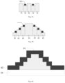
- a plurality of guide structures 01 are formed, and any one of the plurality of guide structures 01 extends in a first direction X, as shown in FIG. 2 A ; and the materials of the plurality of guide structures may be the same.
- FIG. 3 A is a cross-sectional diagram of the plurality of guide structures shown in FIG. 2 A , along a direction AA′. As shown in FIG. 3 A , a cross section of the plurality of guide structures 01 perpendicular to the first direction includes at least one concave-convex structure.
- a guide structure with an integrated structure may also be formed directly, and a top surface extending in the first direction of the guide structure includes the concave-convex structure shown in FIG. 3 A .
- a plurality of guide structures 01 are formed, and any one of the plurality of guide structures 01 extends in a first direction X, as shown in FIG. 2 B ; and the materials of the plurality of guide structures may be the same.
- FIG. 3 B is a cross-sectional diagram of the plurality of guide structures shown in FIG. 2 B , along a direction AA′. As shown in FIG.
- a cross section of the guide structures 01 perpendicular to the first direction include is a stepped structure including at least one step; and one catalyst particle 021 is formed on each step of the stepped structure, and a cross-sectional dimension of the catalyst particle 021 perpendicular to the first direction X is not greater than a cross-sectional dimension of the step where catalyst particle is located.
- a guide structure with an integrated structure may also be formed directly, and a top surface extending in the first direction of the guide structure includes the stepped structure with at least one step shown in FIG. 3 B .
- the cross section of the guide structures 01 perpendicular to the first direction include a concave-convex structure or a stepped structure with at least one step, so that multi-level distribution of silicon-based nanowires can be achieved, thereby solving the heat dissipation problem while increasing a channel width.
- the cross section of the plurality of guide structures perpendicular to the first direction may include both a concave-convex structure and a stepped structure, which is not limited here.
- the plurality of guide structures may be fabricated at separate times, such as forming a plurality of strip-like structures respectively; if the materials of the plurality of guide structures are the same, they may also finally form an integrated structure; the plurality of guide structures may also be patterned after one film forming process, thus being formed into one piece.
- a side surface, extending in the first direction, of each guide structure may also be a flat surface.
- an included angle between the side surface and a bottom surface is preferably greater than or equal to 60°, which can ensure that the subsequent amorphous silicon film can cover the catalyst particle at the side surface of the guide structure, to ensure normal growth of the silicon-based nanowire.
- the pattern of the first active layer is formed after the pattern of the first gate electrode is formed.
- the formation of the plurality of guide structures includes:
- patterning the first gate insulating layer to form the guide structure(s) can avoid the increase in the thickness of the array substrate caused by separately adding a film layer for preparing the guide structure(s).
- the pattern of the first active layer is formed after the pattern of the first gate electrode is formed.
- the formation of the plurality of guide structures specifically includes:
- the pattern of the first gate electrode including a concave-convex structure in a cross section perpendicular to the first direction, or forming the pattern of the first gate electrode including a stepped structure with at least one step in a cross section perpendicular to the first direction;
- the pattern of the first gate electrode and the first gate insulating layer covering the first gate electrode form the guide structures.
- a surface of the first gate electrode is patterned to form the plurality of guide structures, and the first gate insulating layer covering the first gate electrode has corresponding structures as the first gate electrode has the contour of the guide structures.
- the first gate insulating layer may be also used as a gate insulating layer of the second thin film.
- the pattern of the first active layer is formed before the pattern of the first gate electrode is formed.
- the formation of the plurality of guide structures specifically includes: forming a dielectric layer on the base substrate, and patterning the dielectric layer to form the plurality of guide structures.
- the dielectric layer may be formed by a deposition method, which is not limited here.
- the material of the dielectric layer may be aluminum oxide (AlOx), silicon oxide (SiOx), or silicon nitride (SiNx), which is not limited here.
- the dielectric layer may be a buffer layer of the array substrate.
- a buffer layer may also be formed on the base substrate before the formation of the dielectric layer, which is not limited here.
- the material of the catalyst particle includes indium, tin, nickel, or indium oxide, which is not limited here.
- the particle diameter of the catalyst particle may be controlled to 5 nm-10 ⁇ m, such as 5 nm, 10 nm, 50 nm, 100 nm, 500 nm, 1 ⁇ m, or 10 ⁇ m, which is not limited here.
- forming the pattern of the catalyst particle(s) includes:
- forming the pattern of the catalyst particle(s) specifically includes:
- FIG. 4 d is a cross-sectional diagram of FIG. 5 c along a direction B-B′.
- using the nanoimprint process to form the pattern of the catalyst particle(s) can achieve high refineness of the pattern and ensure the uniformity and controllability of the catalyst particle, to ensure uniform growth of the silicon-based nanowire(s).
- the width of the catalyst line is controlled to 50 nm-1000 nm, such as 50 nm, 100 nm, 500 nm, or 1000 nm, which is not limited here.
- the particle diameter of the catalyst particle is determined according to the width of the silicon-based nanowire. Generally, the particle diameter of the catalyst particle is approximately close to the width of the silicon-based nanowire.
- the pattern of the catalyst particle may also be formed by a lithography process. Therefore, optionally, in the preparation method provided by some embodiments of the present disclosure, forming the pattern of the catalyst particle(s) includes:
- etching the catalyst film layer by using the pattern of the photoresist particle(s) as a mask pattern, to form the pattern of the catalyst particle(s).
- the catalyst particle is formed at one end in the extending direction of the guide structure, which can ensure that the silicon-based nanowire extends and grows from one end to the other end of the guide structure.
- the guide structure may be rectilinear or curvilinear along the extending direction, which is not limited here.
- the structure of the first thin film transistor formed may be a bottom-gate structure, or may also be a top-gate structure; similarly, the structure of the second thin film transistor formed may be a bottom-gate structure, or may also be a top-gate structure, which is not limited here.
- the structures of the first thin film transistor and the second thin film transistor formed are both bottom-gate structures, or both top-gate structures. Film layers made of a same material and having a same function may be formed by one patterning process.
- some embodiments provided by the present disclosure include the following steps.
- Step 1 as shown in FIG. 6 A , patterns of a first gate electrode 11 and a second gate electrode 21 are formed on a base substrate 10 by one patterning process.
- the material of the gate electrodes may be a metal or alloy such as molybdenum (Mo), aluminum (Al), copper (Cu), or nickel (Ti), and its thickness may be controlled to 50 nm-5000 nm, which is not limited here.
- Mo molybdenum
- Al aluminum
- Cu copper
- Ti nickel
- Step 2 as shown in FIG. 6 B , a gate insulating layer 30 is formed.
- the material of the gate insulating layer is a dielectric material, and its thickness may be controlled to 50 nm-5000 nm, which is not limited here.
- Step 3 as shown in FIG. 6 C , a pattern of a guide structure 01 is formed in the gate insulating layer 30 .
- the number of the guide structure may be one or more, which is not limited here.
- each guide structure extends in a first direction, and a side surface, extending in the first direction, of the guide structure may include a stepped structure or be a flat surface having an included angle with a bottom surface of greater than or equal to 60 degrees, or a surface, extending in the first direction, of the guide structure may include a concave-convex structure, which is not limited here.
- Step 4 as shown in FIG. 6 D , a pattern of a catalyst particle 021 is formed on at least one side of the guide structure 01 .
- an imprint resist may be formed on a catalyst film layer, and a nanoimprint process is performed on the imprint resist to form a pattern of an imprint resist particle; and the catalyst film layer is etched by using the pattern of the imprint resist particle as a mask pattern to form the pattern of the catalyst particle.
- a nanoimprint process is performed on the imprint resist to form a pattern of an imprint resist line; the catalyst film layer is etched by using the pattern of the imprint resist line as a mask pattern to form a pattern of a catalyst line; a plasma bombardment is performed on the catalyst line to form the pattern of the catalyst particle.
- the pattern of the catalyst particle may also be formed by a lithography process.
- the particle diameter of the catalyst particle may be controlled to 5 nm-10 ⁇ 1, such as 5 nm, 10 nm, 50 nm, 100 nm, 500 nm, 1 ⁇ 0, or 10 ⁇ 0, which is not limited here.
- the material of the catalyst particle includes indium, tin, nickel, or indium oxide, which is not limited here.
- Step 5 as shown in FIG. 6 E , an amorphous silicon film 40 covering the catalyst particle 021 and the guide structure 01 is formed; and the amorphous silicon film 40 is annealed, so that amorphous silicon starts to grow from the catalyst particle 021 in the extending direction of the guide structure 01 to form a silicon-based nanowire 41 .
- a plasma enhanced chemical vapor deposition (PECVD) method is used to deposit the amorphous silicon film of 5 nm ⁇ 5000 nm, and further the thickness of the amorphous silicon film may be controlled to 10 nm ⁇ 1000 nm, which is not limited here.
- PECVD plasma enhanced chemical vapor deposition
- the eutectic point of the catalyst particle and silicon may be within a temperature range of 200° C. ⁇ 1000° C., and an annealing temperature may be controlled to 200° C. ⁇ 600° C., which is not limited here. Further, the annealing temperature may be controlled to 250° C. ⁇ 450° C.
- Step 6 as shown in FIG. 6 F , the catalyst particle 021 is removed, and the amorphous silicon film (not shown in the figure) and the silicon-based nanowire 41 in a first preset area are retained to form a pattern of a first active layer 12 .
- Step 7 as shown in FIG. 6 G , a pattern of a second active layer 22 is formed.
- the material of the second active layer is a carbon nanotube material, and may be formed by spin coating and patterned etching processes, and the thickness of the material of the second active layer is controlled to 1 nm ⁇ 1000 nm.
- the material of the second active layer is an oxide semiconductor material, and may be formed by deposition and patterned etching processes.
- Step 8 as shown in FIG. 6 H , patterns of a first source electrode 13 , a first drain electrode 14 , a second source electrode 23 , and a second drain electrode 24 are formed by one patterning process.
- the materials of the source electrodes and the drain electrodes may be a metal or alloy such as molybdenum (Mo), aluminum (Al), copper (Cu), or nickel (Ti), which is not limited here.
- Mo molybdenum
- Al aluminum
- Cu copper
- Ti nickel
- the method may also include forming a pattern of an etch barrier layer 50 .
- the first source electrode 13 and the first drain electrode 14 are connected with the first active layer 12 through via holes running through the etch barrier layer 50
- the second source electrode 23 and the second drain electrode 24 are connected with the second active layer 22 through via holes running through the etch barrier layer 50 .
- the material of the etch barrier layer is a dielectric material, such as silicon nitride (SiNx), silicon oxide (SiOx), or aluminum oxide (AlOx), and its thickness may be controlled to 50 nm ⁇ 5000 nm, which is not limited here.
- step 7 may be prior to steps 5 and step 6.
- the method includes:
- Step 6′ an excimer laser annealing treatment is performed on the amorphous silicon film formed with the silicon-based nanowire, so that the amorphous silicon film is converted into a low-temperature polysilicon film;
- Step 7′ the catalyst particle is removed, the low-temperature polysilicon film is patterned, the silicon-based nanowire and the low-temperature polysilicon film in a first preset area is retained to form a pattern of a first active layer, and the low-temperature polysilicon film in a second preset area is retained to form a pattern of a second active layer.
- the patterns of the first active layer and the second active layer may be formed by one patterning process, and in the case where the width of the silicon-based nanowire differs greatly from that of the polysilicon film, the patterns may be formed by one patterning process using a gray-tone mask or a half-tone mask, and of course, may also be formed by two patterning processes, which is not limited here.
- the guide structure 01 may also be composed of the first gate electrode 11 and the gate insulating layer 30 . That is, in step 1, the pattern of the first gate electrode 11 is prepared to be similar to the pattern of the guide structure 01 , and in step 2, the gate insulating layer 30 is formed on the first gate electrode 11 such that the gate insulating layer 30 has a pattern corresponding to the first gate electrode 11 . In this way, the process of patterning the gate insulating layer 30 in step 3 may be omitted.
- first thin film transistor and the second thin film transistor being both top-gate structures as an example, some embodiments provided by the present disclosure specifically include the following steps.
- Step 01 a pattern of a guide structure 01 is formed.
- FIG. 9 A a dashed rectangular box indicates a concave portion of the guide structure 01
- FIG. 9 B is a cross-sectional diagram of FIG. 9 A along a direction BB′.
- the guide structure is made of a dielectric material, such as SiOx, SiNx, or Al 2 O 3 , and its thickness is controlled to 20 nm ⁇ 5000 nm, which is not limited here.
- Step 02 as shown in FIGS. 9 A and 9 B , a pattern of a catalyst particle 021 is formed on at least one side of the guide structure 01 . Specifically, a pattern of a catalyst particle 021 is formed at a concave portion or step portion of the guide structure 01 .
- Step 03 as shown in FIG. 9 C , an amorphous silicon film 40 covering the catalyst particle 021 and the guide structure 01 is formed; and the amorphous silicon film 40 is annealed, so that amorphous silicon starts to grow from the catalyst particle 021 in the extending direction of the guide structure 01 to form a silicon-based nanowire 41 .
- Step 04 as shown in FIG. 9 D , the catalyst particle 021 is removed, and the amorphous silicon film (not shown in the figure) and the silicon-based nanowire 41 in a first preset area are retained to form a pattern of a first active layer 12 .
- Step 05 as shown in FIG. 9 E , a pattern of a second active layer 22 is formed.
- Step 06 as shown in FIG. 9 F a gate insulating layer 30 is formed.
- Step 07 as shown in FIG. 9 G , patterns of a first gate electrode 11 and a second gate electrode 12 are formed.
- Step 08 as shown in FIG. 9 H , a pattern of an etch barrier layer 50 is formed.
- Step 09 as shown in FIG. 9 I , patterns of a first source electrode 13 , a first drain electrode 14 , a second source electrode 23 , and a second drain electrode 24 are formed by one patterning process.
- the first source electrode 13 and the first drain electrode 14 are connected with the first active layer 12 through via holes running through the etch barrier layer 50 and the gate insulating layer 30
- the second source electrode 23 and the second drain electrode 24 are connected with the second active layer 22 through via holes running through the etch barrier layer 50 and the gate insulating layer 30 .
- a buffer layer may also be formed before the guide structure is formed, to isolate impurities in the base substrate.
- the buffer layer may also be patterned to form the guide structure.
- the buffer layer is formed of silicon nitride (SiNX) or silicon oxide (SiOx), and its thickness is controlled to 10 nm ⁇ 1000 nm, and then the guide structure is formed by a patterning process. In this way, not only can the buffer layer isolate impurities in the base substrate, but also a separate film layer for fabricating the guide structure can be omitted.
- the top-gate thin film transistor and the bottom-gate thin film transistor only differ in the order of fabrication of the film layers. Therefore, for the preparation of the film layers in the above-mentioned top-gate thin film transistor, reference may be made to the preparation of the film layers with the same functions in the above-mentioned bottom-gate thin film transistor.
- the method further includes forming a planarization layer 60 , an electrode layer 70 and the like on the base substrate 10 , which is not limited here.
- the present disclosure is not limited to the above-mentioned structures, and is also suitable for a TFT structure in which the first thin film transistor is a bottom-gate transistor and the second thin film transistor is a top-gate transistor, or the first thin film transistor is a top-gate transistor and the second thin film transistor is a bottom-gate transistor, which can be understood by those skilled in the art without knowledge creation, and will not be detailed here.
- embodiments of the present disclosure further provide an array substrate, which is prepared by using any of the above-mentioned preparation methods provided by embodiments of the present disclosure; as shown in FIGS. 6 H, 7 and 9 I , the array substrate includes a first thin film transistor and a second thin film transistor on a base substrate 10 ; the first thin film transistor includes a first gate electrode 11 , a first active layer 12 , a first source electrode 13 and a first drain electrode 14 ; and the second thin film transistor includes a second gate electrode 21 , a second active layer 22 , a second source electrode 23 and a second drain electrode 24 .
- At least one guide structure 01 extending in a first direction is disposed under the first active layer 12 , and the material of the first active layer 12 includes a silicon-based nanowire, and an extending direction of the silicon-based nanowire is same as the extending direction of the guide structure 01 .
- the material of the second active layer 22 is different from that of the first active layer 12 .
- the material of the second active layer may be a low-temperature polysilicon material, a carbon nanotube material or an oxide semiconductor material.
- the length of the guide structure 01 along the first direction X is greater than the length of the silicon-based nanowire along the first direction X, and the guide structure 01 extends along the first direction X; and an extending direction of the silicon-based nanowire 41 is same as the extending direction of the guide structure 01 , and is a connecting line direction of the first source electrode 13 and the first drain electrode 14 .
- FIGS. 11 A and 11 B are only for illustrating the positional relationship of the silicon-based nanowire 41 in the first thin film transistor.
- embodiments of the present disclosure further provide a display panel, which includes the above-mentioned array substrate provided by embodiments of the present disclosure.
- the display panel may be a mobile phone, a tablet computer, a television, a display, a notebook computer, a digital photo frame, a navigator, or any other product or component with a display function.
- the display device reference may be made to the embodiments of the above-mentioned array substrate, and repeated description is omitted here.
- the first thin film transistor may be located in a border area of the display panel, so that the width of the border may be reduced.
- Embodiments of the present disclosure provide an array substrate, a method for preparing the array substrate, and a display panel.
- the method includes: forming a first thin film transistor and a second thin film transistor on a base substrate.
- a driving factor that the Gibbs free energy of amorphous silicon is greater than that of crystalline silicon (silicon-based nanowire) by using an eutectic point of the catalyst particle and silicon, and a driving factor that the Gibbs free energy of amorphous silicon is greater than that of crystalline silicon (silicon-based nanowire), and due to absorption of the amorphous silicon by the molten catalyst particle to form a supersaturated silicon eutectoid, the silicon nucleates and grows into a silicon-based nanowire.
- the amorphous silicon film grows linearly along guide structure under the action of the catalyst particle, thus obtaining a silicon-based nanowire with a high density and high uniformity.
- the width of the silicon-based nanowire may also be controlled. In this way, a thin film transistor having a silicon-based nanowire with a uniform and controllable size is prepared.
- the first active layer and the second active layer are made by different materials, such that different thin film transistors have different advantages to increase the application range of the array substrate.
Landscapes
- Thin Film Transistor (AREA)
Abstract
This disclosure provides an array substrate, a method for preparing the array substrate, and a display panel. The method includes: forming a first thin film transistor and a second thin film transistor on a base substrate. In the formation of an active layer of the first thin film transistor, by using an eutectic point of the catalyst particle and silicon, and a driving factor that the Gibbs free energy of amorphous silicon is greater than that of crystalline silicon (silicon-based nanowire), and due to absorption of the amorphous silicon by the molten catalyst particle to form a supersaturated silicon eutectoid, the silicon nucleates and grows into a silicon-based nanowire. Moreover, during the growth of the silicon-based nanowire, the amorphous silicon film grows linearly along guide structure under the action of the catalyst particle, thus obtaining a silicon-based nanowire with a high density and high uniformity.
Description
This disclosure is a national phase entry under 35 U.S.C. § 371 of International Application No. PCT/CN2020/081172, filed on Mar. 25, 2020, which claims priority to Chinese Patent Application No. 201910392488.X filed with the China National Intellectual Property Administration on May 13, 2019 and entitled “Array Substrate, Preparation Method Thereof, and Display Panel”, the entire contents of which are incorporated herein by reference.
The present disclosure relates to the field of semiconductor technology, in particular to an array substrate, a preparation method thereof, and a display panel.
Silicon-based nanowires are a new type of silicon-based semiconductor material developed in recent years, and have a one-dimensional size structure and more excellent semiconductor characteristics. The use of silicon-based nanowire as thin film transistor channels can achieve higher mobility and more stable characteristics.
When the silicon-based nanowires are used as a material of the thin film transistor channels, the size uniformity and controllability are particularly important. Therefore, to meet the uniformity requirement of display devices, how to obtain a thin film transistor having a silicon-based nanowire with a uniform and controllable size has become a hot research topic.
A method for preparing an array substrate provided by embodiments of the present disclosure includes: forming a first thin film transistor and a second thin film transistor on a base substrate.
The forming the first thin film transistor includes forming a pattern of a first gate electrode, a pattern of a first active layer, a pattern of a first source electrode, and a pattern of a first drain electrode on the base substrate.
The forming the second thin film transistor includes forming a pattern of a second gate electrode, a pattern of a second active layer, a pattern of a second source electrode, and a pattern of a second drain electrode on the base substrate.
The material of the first active layer is different from that of the second active layer.
The forming the pattern of the first active layer includes:
forming a guide structure;
forming a pattern of at least one catalyst particle on at least one side of the guide structure, the catalyst particle and silicon having a eutectic point;
forming an amorphous silicon film covering the catalyst particle and the guide structure;
annealing the amorphous silicon film so that amorphous silicon grows from the catalyst particle in an extending direction of the guide structure to form a silicon-based nanowire; and removing the catalyst particle and retaining the amorphous silicon film and the silicon-based nanowire in a first preset area to form the pattern of the first active layer, the catalyst particle being outside the first preset area.
Optionally, in the method provided by some embodiments of the present disclosure, the material of the second active layer is a low-temperature polysilicon material, a carbon nanotube material, or an oxide semiconductor material.
Optionally, in the method provided by some embodiments of the present disclosure, the pattern of the first gate electrode and the pattern of the second gate electrode are formed by one patterning process.
The pattern of the first source electrode, the pattern of the first drain electrode, the pattern of the second source electrode, and the pattern of the second drain electrode are simultaneously formed by one patterning process.
Optionally, in the method provided by some embodiments of the present disclosure, the material of the second active layer is a low-temperature polysilicon material.
The pattern of the second active layer is formed while the pattern of the first active layer is formed, by:
after annealing the amorphous silicon film, excimer laser annealing the amorphous silicon film formed with the silicon-based nanowire, so that the amorphous silicon film is converted into a low-temperature polysilicon film; and
when removing the catalyst particle and patterning the low-temperature polysilicon film, retaining the low-temperature polysilicon film in a second preset area to form the pattern of the second active layer.
Optionally, in the method provided by some embodiments of the present disclosure, a plurality of guide structures are formed, and any one of the plurality of guide structures extends in a first direction; a cross section of the plurality of guide structures perpendicular to the first direction includes a concave-convex structure; and concave portions of the concave-convex structure each has a respective one of the at least one catalyst particle formed therein.
Optionally, in the method provided by some embodiments of the present disclosure, a plurality of guide structures are formed, and any one of the plurality of guide structures extends in a first direction; a cross section of the plurality of guide structures perpendicular to the first direction includes a stepped structure including at least one step, and the at least one step of the stepped structure each is formed with a respective one of the at least one catalyst particle.
Optionally, in the method provided by some embodiments of the present disclosure, the pattern of the first active layer is formed after the pattern of the first gate electrode is formed.
The forming the plurality of guide structures includes:
forming a first gate insulating layer after the pattern of the first gate electrode is formed and before the pattern of the first active layer is formed; and
patterning the first gate insulating layer to form the plurality of guide structures.
Optionally, in the method provided by some embodiments of the present disclosure, the pattern of the first active layer is formed after the pattern of the first gate electrode is formed.
The forming the plurality of guide structures includes:
forming the pattern of the first gate electrode including a concave-convex structure in a cross section perpendicular to the first direction, or forming the pattern of the first gate electrode including a stepped structure with at least one step in a cross section perpendicular to the first direction; and
forming a first gate insulating layer after the pattern of the first gate electrode is formed and before the pattern of the first active layer is formed, the pattern of the first gate electrode and the first gate insulating layer covering the first gate electrode form the plurality of guide structures.
Optionally, in the method provided by some embodiments of the present disclosure, the pattern of the first active layer is formed before the pattern of the first gate electrode is formed.
The forming the plurality of guide structures includes: forming a dielectric layer on the base substrate, and patterning the dielectric layer to form the plurality of guide structures.
Optionally, in the method provided by some embodiments of the present disclosure, the material of the catalyst particle includes indium, tin, nickel or indium oxide.
Optionally, in the method provided by some embodiments of the present disclosure, a particle diameter of the catalyst particle is 5 nm-10 μm.
Optionally, in the method provided by some embodiments of the present disclosure, the forming the pattern of at least one catalyst particle includes:
forming a catalyst film layer on the base substrate formed with the guide structure;
forming an imprint resist on the catalyst film layer;
nano-imprinting the imprint resist to form a pattern of an imprint resist particle; and
etching the catalyst film layer by using the pattern of the imprint resist particle as a mask pattern, to form the pattern of the catalyst particle.
Optionally, in the method provided by some embodiments of the present disclosure, the forming the pattern of the at least one catalyst particle includes:
forming a catalyst film layer on the base substrate formed with the guide structure;
forming an imprint resist on the catalyst film layer;
nano-imprinting the imprint resist to form a pattern of an imprint resist line, wherein an extending direction of the imprint resist line is perpendicular to the extending direction of the guide structure;
etching the catalyst film layer by using the pattern of the imprint resist line as a mask pattern, to form a pattern of a catalyst line; and
performing plasma bombardment on the catalyst line to form the pattern of the catalyst particle.
Optionally, in the method provided by some embodiments of the present disclosure, the eutectic point of the catalyst particles and silicon is within a temperature range of 200° C.˜1000° C.
While annealing the amorphous silicon film, an annealing temperature is 200° C.˜600° C.
Correspondingly, embodiments of the present disclosure further provide an array substrate, which is prepared by any of the above-mentioned methods provided by embodiments of the present disclosure.
The array substrate includes:
the first thin film transistor on a base substrate, the first thin film transistor including the first gate electrode, the first active layer, the first source electrode and the first drain electrode, wherein at least one guide structure extending in a first direction is disposed under the first active layer, and the material of the first active layer includes a silicon-based nanowire, and an extending direction of the silicon-based nanowire is same as the extending direction of the guide structure; and
a second thin film transistor on the base substrate, the second thin film transistor including the second gate electrode, the second active layer, the second source electrode and the second drain electrode, the material of the second active layer being different from that of the first active layer.
Optionally, in the array substrate provided by some embodiments of the present disclosure, the length of the guide structure along the first direction is greater than the length of the silicon-based nanowire along the first direction.
Optionally, in the array substrate provided by some embodiments of the present disclosure, a connecting line direction of the first source electrode and the first drain electrode is same as the extending direction of the silicon-based nanowire.
Optionally, in the array substrate provided by some embodiments of the present disclosure, the material of the second active layer is a low-temperature polysilicon material, a carbon nanotube material, or an oxide semiconductor material.
Correspondingly, embodiments of the present disclosure further provide a display panel, which includes the above-mentioned array substrate provided by embodiments of the present disclosure.
To make the objects, technical solutions and advantages of the present disclosure clearer, the present disclosure will be further described in detail below in conjunction with the accompanying drawings. Apparently, the embodiments described are part of, rather than all of, the embodiments of the present disclosure. Based on the embodiments of the present disclosure, all other embodiments obtained by those of ordinary skill in the art without creative work shall fall within the protection scope of the present disclosure.
The shapes and sizes of the components in the drawings do not reflect the true scale, and are merely intended to illustrate the present disclosure.
A method for preparing an array substrate provided by embodiments of the present disclosure includes forming a first thin film transistor and a second thin film transistor on a base substrate.
The step of forming the first thin film transistor includes forming a pattern of a first gate electrode, a pattern of a first active layer, a pattern of a first source electrode, and a pattern of a first drain electrode on the base substrate.
The step of forming the second thin film transistor includes forming a pattern of a second gate electrode, a pattern of a second active layer, a pattern of a second source electrode, and a pattern of a second drain electrode on the base substrate.
The material of the first active layer is different from that of the second active layer.
The step of forming the pattern of the first active layer, as shown in FIG. 1 , includes:
S101. forming a guide structure;
S102. forming a pattern of at least one catalyst particle on at least one side of the guide structure, the catalyst particle and silicon having a eutectic point;
S103. forming an amorphous silicon film covering the catalyst particle and the guide structure;
S104. annealing the amorphous silicon film so that amorphous silicon grows from the catalyst particle in an extending direction of the guide structure to form a silicon-based nanowire; and
S105. removing the catalyst particle and retaining the amorphous silicon film and the silicon-based nanowire in a first preset area to form the pattern of the first active layer, wherein the catalyst particle is outside the first preset area.
The method for preparing an array substrate provided by embodiments of the present disclosure includes forming a first thin film transistor and a second thin film transistor on a base substrate. In the formation of an active layer of the first thin film transistor, by using an eutectic point of the catalyst particle and silicon, and a driving factor that the Gibbs free energy of amorphous silicon is greater than that of crystalline silicon (silicon-based nanowire), and due to absorption of the amorphous silicon by the molten catalyst particle to form a supersaturated silicon eutectoid, the silicon nucleates and grows into a silicon-based nanowire. Moreover, during the growth of the silicon-based nanowire, the amorphous silicon film grows linearly along the guide structure under the action of the catalyst particle, thus obtaining a silicon-based nanowire with a high density and high uniformity. In addition, by controlling the size of the catalyst particle and the thickness of the amorphous silicon film, the width of the silicon-based nanowire may also be controlled. In this way, a thin film transistor having a silicon-based nanowire with a uniform and controllable size is prepared.
In addition, the first active layer and the second active layer are made by different materials, such that different thin film transistors have different advantages to increase the application range of the array substrate.
In specific implementation, as the silicon-based nanowire has more excellent semiconductor characteristics and smaller size dimensions than polycrystalline silicon, the size of the first thin film transistor may be made relatively smaller, and thus applying the first thin film transistor in a border area of a panel can achieve a smaller border size; applying the first thin film transistor in a switching transistor can achieve a faster switching speed and a higher refresh frequency; and in the case where the first thin film transistor is used for a large-size transistor in a back plate, it can prevent a semiconductor layer from generating heat to cause device characteristic drift.
Optionally, in the preparation method provided by some embodiments of the present disclosure, the material of the second active layer is any one or more of a low-temperature polysilicon material, a carbon nanotube material or an oxide semiconductor material.
In specific implementation, low-temperature polysilicon has high mobility and stability, the uniformity is more difficult to control in a large-size panel adopting low-temperature polysilicon. A carbon nanotube also has high mobility and can achieve flexible display. An oxide semiconductor material is relatively low in mobility, but can ensure good uniformity in a large-size panel, and is low in leakage current, transparent, and simple in manufacturing process. Therefore, the material of the second active layer can be selected according to actual requirements. The second active layer is used in conjunction with the first active layer to meet different circuit requirements, such as adjusting a sub-threshold swing SS of the thin film transistor, an off-state current Ioff of the thin film transistor, and the mobility of the thin film transistor.
In specific implementation, to simplify the manufacturing process and save the production cost, in the first thin film transistor and the second thin film transistor, film layers with a same function are prepared in a same layer as much as possible.
Optionally, in the preparation method provided by some embodiments of the present disclosure, the pattern of the first gate electrode and the pattern of the second gate electrode are formed by one patterning process.
The pattern of the first source electrode, the pattern of the first drain electrode, the pattern of the second source electrode, and the pattern of the second drain electrode are simultaneously formed by one patterning process.
In specific implementation, in the above-mentioned preparation method provided by some embodiments of the present disclosure, in the case where the material of the second active layer is a low-temperature polysilicon material, to simplify process steps and save the production cost, the first active layer and the second active layer may be prepared by using a same layer of amorphous silicon film.
Specifically, in the preparation method provided by some embodiments of the present disclosure, the material of the second active layer is a low-temperature polysilicon material.
The pattern of the first active layer and the pattern of the second active layer are formed simultaneously by one patterning process, by:
after annealing the amorphous silicon film, performing an excimer laser annealing treatment on the amorphous silicon film formed with the silicon-based nanowire, so that the amorphous silicon film is converted into a low-temperature polysilicon film;
removing the catalyst particle, patterning the low-temperature polysilicon film, retaining the silicon-based nanowire and the low-temperature polysilicon film in a first preset area to form the pattern of the first active layer, and retaining the low-temperature poly silicon film in a second preset area to form the pattern of the second active layer.
It should be noted that in the preparation method provided by some embodiments of the present disclosure, the first preset area is an area for forming the first active layer, and the second present area is an area for forming the second active layer.
Specifically, in the preparation method provided by some embodiments of the present disclosure, the more guide structures, the more silicon-based nanowires are formed, and thus forming a plurality of guide structures can ensure there are a plurality of silicon-based nanowires in the first active layer, thereby improving the mobility of the first thin film transistor.
Optionally, in the preparation method provided by some embodiments of the present disclosure, a plurality of guide structures 01 are formed, and any one of the plurality of guide structures 01 extends in a first direction X, as shown in FIG. 2A ; and the materials of the plurality of guide structures may be the same. FIG. 3A is a cross-sectional diagram of the plurality of guide structures shown in FIG. 2A , along a direction AA′. As shown in FIG. 3A , a cross section of the plurality of guide structures 01 perpendicular to the first direction includes at least one concave-convex structure. In the concave-convex structure, surfaces of all convex portions are almost equal-height, and surfaces of all concave portions are almost equal-height; and one catalyst particle 021 is formed in each concave portion of the concave-convex construction, and a cross-sectional dimension of the catalyst particle 021 perpendicular to the first direction X is not greater than a cross-sectional dimension of the concave portion where catalyst particle is located.
It should be noted that a guide structure with an integrated structure may also be formed directly, and a top surface extending in the first direction of the guide structure includes the concave-convex structure shown in FIG. 3A .
Optionally, in the preparation method provided by some embodiments of the present disclosure, a plurality of guide structures 01 are formed, and any one of the plurality of guide structures 01 extends in a first direction X, as shown in FIG. 2B ; and the materials of the plurality of guide structures may be the same. FIG. 3B is a cross-sectional diagram of the plurality of guide structures shown in FIG. 2B , along a direction AA′. As shown in FIG. 3B , a cross section of the guide structures 01 perpendicular to the first direction include is a stepped structure including at least one step; and one catalyst particle 021 is formed on each step of the stepped structure, and a cross-sectional dimension of the catalyst particle 021 perpendicular to the first direction X is not greater than a cross-sectional dimension of the step where catalyst particle is located. It may be understood that a guide structure with an integrated structure may also be formed directly, and a top surface extending in the first direction of the guide structure includes the stepped structure with at least one step shown in FIG. 3B .
In specific implementation, as shown in FIGS. 3A and 3B , the cross section of the guide structures 01 perpendicular to the first direction include a concave-convex structure or a stepped structure with at least one step, so that multi-level distribution of silicon-based nanowires can be achieved, thereby solving the heat dissipation problem while increasing a channel width.
Of course, in specific implementation, the cross section of the plurality of guide structures perpendicular to the first direction may include both a concave-convex structure and a stepped structure, which is not limited here.
It may be understood that the plurality of guide structures may be fabricated at separate times, such as forming a plurality of strip-like structures respectively; if the materials of the plurality of guide structures are the same, they may also finally form an integrated structure; the plurality of guide structures may also be patterned after one film forming process, thus being formed into one piece.
It should be noted that in the preparation method provided by some embodiments of the present disclosure, a side surface, extending in the first direction, of each guide structure may also be a flat surface. In specific implementation, an included angle between the side surface and a bottom surface is preferably greater than or equal to 60°, which can ensure that the subsequent amorphous silicon film can cover the catalyst particle at the side surface of the guide structure, to ensure normal growth of the silicon-based nanowire.
Optionally, in the preparation method provided by some embodiments of the present disclosure, the pattern of the first active layer is formed after the pattern of the first gate electrode is formed.
The formation of the plurality of guide structures includes:
forming a first gate insulating layer after the pattern of the first gate electrode is formed and before the pattern of the first active layer is formed; and
patterning the first gate insulating layer to form the guide structures.
In specific implementation, patterning the first gate insulating layer to form the guide structure(s) can avoid the increase in the thickness of the array substrate caused by separately adding a film layer for preparing the guide structure(s).
Optionally, in the preparation method provided by some embodiments of the present disclosure, the pattern of the first active layer is formed after the pattern of the first gate electrode is formed.
The formation of the plurality of guide structures specifically includes:
forming the pattern of the first gate electrode including a concave-convex structure in a cross section perpendicular to the first direction, or forming the pattern of the first gate electrode including a stepped structure with at least one step in a cross section perpendicular to the first direction; and
forming a first gate insulating layer after the pattern of the first gate electrode is formed and before the pattern of the first active layer is formed, the pattern of the first gate electrode and the first gate insulating layer covering the first gate electrode form the guide structures.
In specific implementation, a surface of the first gate electrode is patterned to form the plurality of guide structures, and the first gate insulating layer covering the first gate electrode has corresponding structures as the first gate electrode has the contour of the guide structures. Forming the guide structures by using the pattern of the first gate electrode can avoid the increase in the thickness of the array substrate caused by separately adding a film layer for preparing the guide structures, and this does not need to add a patterning process, and is achieved just by changing the pattern of the existing gate electrode.
In specific implementation, in the preparation method provided by some embodiments of the present disclosure, the first gate insulating layer may be also used as a gate insulating layer of the second thin film.
Optionally, in the preparation method provided by some embodiments of the present disclosure, the pattern of the first active layer is formed before the pattern of the first gate electrode is formed.
The formation of the plurality of guide structures specifically includes: forming a dielectric layer on the base substrate, and patterning the dielectric layer to form the plurality of guide structures.
In specific implementation, in the preparation method provided by some embodiments of the present disclosure, the dielectric layer may be formed by a deposition method, which is not limited here.
In specific implementation, the material of the dielectric layer may be aluminum oxide (AlOx), silicon oxide (SiOx), or silicon nitride (SiNx), which is not limited here.
Further, in specific implementation, the dielectric layer may be a buffer layer of the array substrate. Of course, a buffer layer may also be formed on the base substrate before the formation of the dielectric layer, which is not limited here.
Optionally, in the preparation method provided by some embodiments of the present disclosure, the material of the catalyst particle includes indium, tin, nickel, or indium oxide, which is not limited here.
Optionally, in the preparation method provided by some embodiments of the present disclosure, the particle diameter of the catalyst particle may be controlled to 5 nm-10 μm, such as 5 nm, 10 nm, 50 nm, 100 nm, 500 nm, 1 μm, or 10 μm, which is not limited here.
Optionally, in the preparation method provided by some embodiments of the present disclosure, forming the pattern of the catalyst particle(s) includes:
forming a catalyst film layer 02 on the base substrate 10 formed with the guide structure(s) 01, as shown in FIG. 4A ;
forming an imprint resist 03 on the catalyst film layer 02, as shown in FIG. 4B ;
nano-imprinting the imprint resist 03 to form a pattern of imprint resist particle(s) 031, as shown in FIG. 4C ; and
etching the catalyst film layer 02 by using the pattern of the imprint resist particle(s) 031 as a mask pattern, to form the pattern of the catalyst particle(s) 021, as shown in FIG. 4D .
Or optionally, in the preparation method provided by some embodiments of the present disclosure, forming the pattern of the catalyst particle(s) specifically includes:
forming the catalyst film layer 02 on the base substrate 10 formed with the guide structure 01, as shown in FIG. 4A ;
forming an imprint resist 03 on the catalyst film layer 02, as shown in FIG. 4B ;
nano-imprinting the imprint resist 03 to form a pattern of an imprint resist line 032, wherein an extending direction of the imprint resist line 032 is perpendicular to the extending direction of the guide structure 01, as shown in FIG. 5A ;
etching the catalyst film layer 02 by using the pattern of the imprint resist line 032 as a mask pattern, to form a pattern of a catalyst line 022, as shown in FIG. 5B ; and
performing plasma bombardment on the catalyst line to form the pattern of the catalyst particle(s) 021, as shown in FIGS. 5C and 4D . FIG. 4 d is a cross-sectional diagram of FIG. 5 c along a direction B-B′.
In specific implementation, using the nanoimprint process to form the pattern of the catalyst particle(s) can achieve high refineness of the pattern and ensure the uniformity and controllability of the catalyst particle, to ensure uniform growth of the silicon-based nanowire(s).
Optionally, in the preparation method provided by some embodiments of the present disclosure, the width of the catalyst line is controlled to 50 nm-1000 nm, such as 50 nm, 100 nm, 500 nm, or 1000 nm, which is not limited here.
In specific implementation, the particle diameter of the catalyst particle is determined according to the width of the silicon-based nanowire. Generally, the particle diameter of the catalyst particle is approximately close to the width of the silicon-based nanowire.
Of course, in specific implementation, the pattern of the catalyst particle may also be formed by a lithography process. Therefore, optionally, in the preparation method provided by some embodiments of the present disclosure, forming the pattern of the catalyst particle(s) includes:
forming a catalyst film layer on the base substrate formed with the guide structure;
forming a photoresist on the catalyst film layer;
performing an exposure and developing process on the photoresist to form a pattern of photoresist particle(s); and
etching the catalyst film layer by using the pattern of the photoresist particle(s) as a mask pattern, to form the pattern of the catalyst particle(s).
In specific implementation, in the preparation method provided by some embodiments of the present disclosure, the catalyst particle is formed at one end in the extending direction of the guide structure, which can ensure that the silicon-based nanowire extends and grows from one end to the other end of the guide structure.
Further, in the preparation method provided by some embodiments of the present disclosure, the guide structure may be rectilinear or curvilinear along the extending direction, which is not limited here.
In specific implementation, in the preparation method provided by some embodiments of the present disclosure, the structure of the first thin film transistor formed may be a bottom-gate structure, or may also be a top-gate structure; similarly, the structure of the second thin film transistor formed may be a bottom-gate structure, or may also be a top-gate structure, which is not limited here. To simplify the process and reduce the cost, the structures of the first thin film transistor and the second thin film transistor formed are both bottom-gate structures, or both top-gate structures. Film layers made of a same material and having a same function may be formed by one patterning process.
The preparation method provided by embodiments of the present disclosure is described below with specific embodiments.
Using the first thin film transistor and the second thin film transistor being both bottom-gate structures as an example, some embodiments provided by the present disclosure include the following steps.
Step 1: as shown in FIG. 6A , patterns of a first gate electrode 11 and a second gate electrode 21 are formed on a base substrate 10 by one patterning process.
In specific implementation, the material of the gate electrodes may be a metal or alloy such as molybdenum (Mo), aluminum (Al), copper (Cu), or nickel (Ti), and its thickness may be controlled to 50 nm-5000 nm, which is not limited here.
Step 2: as shown in FIG. 6B , a gate insulating layer 30 is formed.
In specific implementation, the material of the gate insulating layer is a dielectric material, and its thickness may be controlled to 50 nm-5000 nm, which is not limited here.
Step 3: as shown in FIG. 6C , a pattern of a guide structure 01 is formed in the gate insulating layer 30.
In specific implementation, the number of the guide structure may be one or more, which is not limited here.
In specific implementation, each guide structure extends in a first direction, and a side surface, extending in the first direction, of the guide structure may include a stepped structure or be a flat surface having an included angle with a bottom surface of greater than or equal to 60 degrees, or a surface, extending in the first direction, of the guide structure may include a concave-convex structure, which is not limited here.
Step 4: as shown in FIG. 6D , a pattern of a catalyst particle 021 is formed on at least one side of the guide structure 01.
In specific implementation, an imprint resist may be formed on a catalyst film layer, and a nanoimprint process is performed on the imprint resist to form a pattern of an imprint resist particle; and the catalyst film layer is etched by using the pattern of the imprint resist particle as a mask pattern to form the pattern of the catalyst particle. Alternatively, a nanoimprint process is performed on the imprint resist to form a pattern of an imprint resist line; the catalyst film layer is etched by using the pattern of the imprint resist line as a mask pattern to form a pattern of a catalyst line; a plasma bombardment is performed on the catalyst line to form the pattern of the catalyst particle. Of course, the pattern of the catalyst particle may also be formed by a lithography process.
Further, the particle diameter of the catalyst particle may be controlled to 5 nm-10μ1, such as 5 nm, 10 nm, 50 nm, 100 nm, 500 nm, 1μ0, or 10μ0, which is not limited here. The material of the catalyst particle includes indium, tin, nickel, or indium oxide, which is not limited here.
Step 5: as shown in FIG. 6E , an amorphous silicon film 40 covering the catalyst particle 021 and the guide structure 01 is formed; and the amorphous silicon film 40 is annealed, so that amorphous silicon starts to grow from the catalyst particle 021 in the extending direction of the guide structure 01 to form a silicon-based nanowire 41.
In specific implementation, a plasma enhanced chemical vapor deposition (PECVD) method is used to deposit the amorphous silicon film of 5 nm˜5000 nm, and further the thickness of the amorphous silicon film may be controlled to 10 nm˜1000 nm, which is not limited here.
In specific implementation, the eutectic point of the catalyst particle and silicon may be within a temperature range of 200° C.˜1000° C., and an annealing temperature may be controlled to 200° C.˜600° C., which is not limited here. Further, the annealing temperature may be controlled to 250° C.˜450° C.
Step 6: as shown in FIG. 6F , the catalyst particle 021 is removed, and the amorphous silicon film (not shown in the figure) and the silicon-based nanowire 41 in a first preset area are retained to form a pattern of a first active layer 12.
Step 7: as shown in FIG. 6G , a pattern of a second active layer 22 is formed.
Specifically, the material of the second active layer is a carbon nanotube material, and may be formed by spin coating and patterned etching processes, and the thickness of the material of the second active layer is controlled to 1 nm˜1000 nm.
Specifically, the material of the second active layer is an oxide semiconductor material, and may be formed by deposition and patterned etching processes.
Step 8: as shown in FIG. 6H , patterns of a first source electrode 13, a first drain electrode 14, a second source electrode 23, and a second drain electrode 24 are formed by one patterning process.
In specific implementation, the materials of the source electrodes and the drain electrodes may be a metal or alloy such as molybdenum (Mo), aluminum (Al), copper (Cu), or nickel (Ti), which is not limited here.
In the above embodiment, as shown in FIG. 7 , before the patterns of the first source electrode 13, the first drain electrode 14, the second source electrode 23, and the second drain electrode 24 are formed, the method may also include forming a pattern of an etch barrier layer 50. The first source electrode 13 and the first drain electrode 14 are connected with the first active layer 12 through via holes running through the etch barrier layer 50, and the second source electrode 23 and the second drain electrode 24 are connected with the second active layer 22 through via holes running through the etch barrier layer 50.
In specific implementation, the material of the etch barrier layer is a dielectric material, such as silicon nitride (SiNx), silicon oxide (SiOx), or aluminum oxide (AlOx), and its thickness may be controlled to 50 nm˜5000 nm, which is not limited here.
It should be noted that in the above-mentioned preparation method provided by the embodiments of the present disclosure, the order of forming the first active layer and the second active layer may be reversed. That is, step 7 may be prior to steps 5 and step 6.
Further, in the above-mentioned preparation method provided by some embodiments of the present disclosure, in the case where the material of the second active layer is a low-temperature polysilicon material, after step 5 and before step 8, the method includes:
Step 6′: an excimer laser annealing treatment is performed on the amorphous silicon film formed with the silicon-based nanowire, so that the amorphous silicon film is converted into a low-temperature polysilicon film; and
Step 7′: the catalyst particle is removed, the low-temperature polysilicon film is patterned, the silicon-based nanowire and the low-temperature polysilicon film in a first preset area is retained to form a pattern of a first active layer, and the low-temperature polysilicon film in a second preset area is retained to form a pattern of a second active layer.
It should be noted that in the case where the width of the silicon-based nanowire is close to that of the polysilicon film, the patterns of the first active layer and the second active layer may be formed by one patterning process, and in the case where the width of the silicon-based nanowire differs greatly from that of the polysilicon film, the patterns may be formed by one patterning process using a gray-tone mask or a half-tone mask, and of course, may also be formed by two patterning processes, which is not limited here.
Further, in the above-mentioned preparation method provided by some embodiments of the present disclosure, as shown in FIG. 8 , the guide structure 01 may also be composed of the first gate electrode 11 and the gate insulating layer 30. That is, in step 1, the pattern of the first gate electrode 11 is prepared to be similar to the pattern of the guide structure 01, and in step 2, the gate insulating layer 30 is formed on the first gate electrode 11 such that the gate insulating layer 30 has a pattern corresponding to the first gate electrode 11. In this way, the process of patterning the gate insulating layer 30 in step 3 may be omitted.
Using the first thin film transistor and the second thin film transistor being both top-gate structures as an example, some embodiments provided by the present disclosure specifically include the following steps.
Step 01: a pattern of a guide structure 01 is formed.
It should be noted that in FIG. 9A , a dashed rectangular box indicates a concave portion of the guide structure 01, and FIG. 9B is a cross-sectional diagram of FIG. 9A along a direction BB′.
In specific implementation, the guide structure is made of a dielectric material, such as SiOx, SiNx, or Al2O3, and its thickness is controlled to 20 nm˜5000 nm, which is not limited here.
Step 02: as shown in FIGS. 9A and 9B , a pattern of a catalyst particle 021 is formed on at least one side of the guide structure 01. Specifically, a pattern of a catalyst particle 021 is formed at a concave portion or step portion of the guide structure 01.
Step 03: as shown in FIG. 9C , an amorphous silicon film 40 covering the catalyst particle 021 and the guide structure 01 is formed; and the amorphous silicon film 40 is annealed, so that amorphous silicon starts to grow from the catalyst particle 021 in the extending direction of the guide structure 01 to form a silicon-based nanowire 41.
Step 04: as shown in FIG. 9D , the catalyst particle 021 is removed, and the amorphous silicon film (not shown in the figure) and the silicon-based nanowire 41 in a first preset area are retained to form a pattern of a first active layer 12.
Step 05: as shown in FIG. 9E , a pattern of a second active layer 22 is formed.
Step 06: as shown in FIG. 9F a gate insulating layer 30 is formed.
Step 07: as shown in FIG. 9G , patterns of a first gate electrode 11 and a second gate electrode 12 are formed.
Step 08: as shown in FIG. 9H , a pattern of an etch barrier layer 50 is formed.
Step 09: as shown in FIG. 9I , patterns of a first source electrode 13, a first drain electrode 14, a second source electrode 23, and a second drain electrode 24 are formed by one patterning process. The first source electrode 13 and the first drain electrode 14 are connected with the first active layer 12 through via holes running through the etch barrier layer 50 and the gate insulating layer 30, and the second source electrode 23 and the second drain electrode 24 are connected with the second active layer 22 through via holes running through the etch barrier layer 50 and the gate insulating layer 30.
In the above-mentioned embodiment, a buffer layer may also be formed before the guide structure is formed, to isolate impurities in the base substrate.
Of course, in specific implementation, the buffer layer may also be patterned to form the guide structure. For example, the buffer layer is formed of silicon nitride (SiNX) or silicon oxide (SiOx), and its thickness is controlled to 10 nm˜1000 nm, and then the guide structure is formed by a patterning process. In this way, not only can the buffer layer isolate impurities in the base substrate, but also a separate film layer for fabricating the guide structure can be omitted.
In specific implementation, in the manufacturing process, the top-gate thin film transistor and the bottom-gate thin film transistor only differ in the order of fabrication of the film layers. Therefore, for the preparation of the film layers in the above-mentioned top-gate thin film transistor, reference may be made to the preparation of the film layers with the same functions in the above-mentioned bottom-gate thin film transistor.
In specific implementation, in the case where the above-mentioned array substrate is applied to a display panel, after the formation of the first thin film transistor and the second thin film transistor, as shown in FIG. 10 , the method further includes forming a planarization layer 60, an electrode layer 70 and the like on the base substrate 10, which is not limited here.
In specific implementation, the present disclosure is not limited to the above-mentioned structures, and is also suitable for a TFT structure in which the first thin film transistor is a bottom-gate transistor and the second thin film transistor is a top-gate transistor, or the first thin film transistor is a top-gate transistor and the second thin film transistor is a bottom-gate transistor, which can be understood by those skilled in the art without knowledge creation, and will not be detailed here.
Based on the same inventive concept, embodiments of the present disclosure further provide an array substrate, which is prepared by using any of the above-mentioned preparation methods provided by embodiments of the present disclosure; as shown in FIGS. 6H, 7 and 9I , the array substrate includes a first thin film transistor and a second thin film transistor on a base substrate 10; the first thin film transistor includes a first gate electrode 11, a first active layer 12, a first source electrode 13 and a first drain electrode 14; and the second thin film transistor includes a second gate electrode 21, a second active layer 22, a second source electrode 23 and a second drain electrode 24.
In the first thin film transistor, at least one guide structure 01 extending in a first direction is disposed under the first active layer 12, and the material of the first active layer 12 includes a silicon-based nanowire, and an extending direction of the silicon-based nanowire is same as the extending direction of the guide structure 01.
The material of the second active layer 22 is different from that of the first active layer 12.
Optionally, in the array substrate provided by the embodiments of the present disclosure, the material of the second active layer may be a low-temperature polysilicon material, a carbon nanotube material or an oxide semiconductor material.
In specific implementation, referring to FIGS. 11A and 11B , in the first thin film transistor, the length of the guide structure 01 along the first direction X is greater than the length of the silicon-based nanowire along the first direction X, and the guide structure 01 extends along the first direction X; and an extending direction of the silicon-based nanowire 41 is same as the extending direction of the guide structure 01, and is a connecting line direction of the first source electrode 13 and the first drain electrode 14. FIGS. 11A and 11B are only for illustrating the positional relationship of the silicon-based nanowire 41 in the first thin film transistor.
In specific implementation, as the problem-solving principle of the array substrate is similar to that of the above-mentioned method for preparing an array substrate, for the implementation of the array substrate, reference may be made to the implementation of the above-mentioned preparation method, and repeated description is omitted.
Based on the same inventive concept, embodiments of the present disclosure further provide a display panel, which includes the above-mentioned array substrate provided by embodiments of the present disclosure. The display panel may be a mobile phone, a tablet computer, a television, a display, a notebook computer, a digital photo frame, a navigator, or any other product or component with a display function. For the implementation of the display device, reference may be made to the embodiments of the above-mentioned array substrate, and repeated description is omitted here.
In specific implementation, the first thin film transistor may be located in a border area of the display panel, so that the width of the border may be reduced.
Embodiments of the present disclosure provide an array substrate, a method for preparing the array substrate, and a display panel. The method includes: forming a first thin film transistor and a second thin film transistor on a base substrate. In the formation of an active layer of the first thin film transistor, by using an eutectic point of the catalyst particle and silicon, and a driving factor that the Gibbs free energy of amorphous silicon is greater than that of crystalline silicon (silicon-based nanowire), and due to absorption of the amorphous silicon by the molten catalyst particle to form a supersaturated silicon eutectoid, the silicon nucleates and grows into a silicon-based nanowire. Moreover, during the growth of the silicon-based nanowire, the amorphous silicon film grows linearly along guide structure under the action of the catalyst particle, thus obtaining a silicon-based nanowire with a high density and high uniformity. In addition, by controlling the size of the catalyst particle and the thickness of the amorphous silicon film, the width of the silicon-based nanowire may also be controlled. In this way, a thin film transistor having a silicon-based nanowire with a uniform and controllable size is prepared. In addition, the first active layer and the second active layer are made by different materials, such that different thin film transistors have different advantages to increase the application range of the array substrate.
Evidently, those skilled in the art can make various modifications and variations to the present disclosure without departing from the spirit and scope of the present disclosure. Thus, the present disclosure is also intended to encompass these modifications and variations thereto so long as the modifications and variations come into the scope of the claims appended to the present disclosure and their equivalents.
Claims (15)
1. A method for preparing an array substrate, comprising:
forming a first thin film transistor and a second thin film transistor on a base substrate;
wherein:
said forming the first thin film transistor comprises:
forming a pattern of a first gate electrode, a pattern of a first active layer, a pattern of a first source electrode, and a pattern of a first drain electrode on the base substrate;
said forming the second thin film transistor comprises:
forming a pattern of a second gate electrode, a pattern of a second active layer, a pattern of a second source electrode, and a pattern of a second drain electrode on the base substrate;
wherein:
a material of the first active layer is different from a material of the second active layer; and
said forming the pattern of the first active layer comprises:
forming a guide structure;
forming a pattern of at least one catalyst particle on at least one side of the guide structure, the catalyst particle and silicon having a eutectic point;
forming an amorphous silicon film covering the catalyst particle and the guide structure;
annealing the amorphous silicon film so that amorphous silicon grows from the catalyst particle in an extending direction of the guide structure to form a silicon-based nanowire; and
removing the catalyst particle and retaining the amorphous silicon film and the silicon-based nanowire in a first preset area to form the pattern of the first active layer, the catalyst particle being outside the first preset area.
2. The method according to claim 1 , wherein the material of the second active layer is:
a low-temperature polysilicon material, or
a carbon nanotube material, or
an oxide semiconductor material.
3. The method according to claim 2 , wherein the pattern of the first gate electrode and the pattern of the second gate electrode are formed by one patterning process; and
the pattern of the first source electrode, the pattern of the first drain electrode, the pattern of the second source electrode, and the pattern of the second drain electrode are simultaneously formed by one patterning process.
4. The method according to claim 3 , wherein the material of the second active layer is the low-temperature polysilicon material; and
the pattern of the second active layer is formed while the pattern of the first active layer is formed, by:
after annealing the amorphous silicon film, excimer laser annealing the amorphous silicon film formed with the silicon-based nanowire, so that the amorphous silicon film is converted into a low-temperature polysilicon film; and
when removing the catalyst particle and patterning the low-temperature polysilicon film, retaining the low-temperature polysilicon film in a second preset area to form the pattern of the second active layer.
5. The method according to claim 1 , wherein a plurality of guide structures are formed, and any one of the plurality of guide structures extends in a first direction; a cross section of the plurality of guide structures perpendicular to the first direction comprise a concave-convex structure; and concave portions of the concave-convex structure each has a respective one of the at least one catalyst particle formed therein.
6. The method according to claim 1 , wherein a plurality of guide structures are formed, and any one of the plurality of guide structures extends in a first direction; a cross section of the plurality of guide structures perpendicular to the first direction comprises a stepped structure comprising at least one step, and the at least one step of the stepped structure each is formed with a respective one of the at least one catalyst particle.
7. The method according to claim 5 , wherein the pattern of the first active layer is formed after the pattern of the first gate electrode is formed; and
said forming the plurality of guide structures comprises:
forming a first gate insulating layer after the pattern of the first gate electrode is formed and before the pattern of the first active layer is formed; and
patterning the first gate insulating layer to form the plurality of guide structures.
8. The method according to claim 5 , wherein the pattern of the first active layer is formed after the pattern of the first gate electrode is formed; and
said forming the plurality of guide structures comprises:
forming the pattern of the first gate electrode comprising a concave-convex structure in a cross section perpendicular to the first direction, or forming the pattern of the first gate electrode comprising a stepped structure with at least one step in a cross section perpendicular to the first direction; and
forming a first gate insulating layer after the pattern of the first gate electrode is formed and before the pattern of the first active layer is formed, the pattern of the first gate electrode and the first gate insulating layer covering the first gate electrode form the plurality of guide structures.
9. The method according to claim 5 , wherein the pattern of the first active layer is formed before the pattern of the first gate electrode is formed; and
said forming the plurality of guide structures comprises:
forming a dielectric layer on the base substrate; and
patterning the dielectric layer to form the plurality of guide structures.
10. The method according to claim 1 , wherein a material of the catalyst particle comprises indium, tin, nickel or indium oxide.
11. The method according to claim 1 , wherein a particle diameter of the catalyst particle is 5 nm˜10 μm.
12. The method according to claim 1 , wherein said forming the pattern of at least one catalyst particle comprises:
forming a catalyst film layer on the base substrate formed with the guide structure;
forming an imprint resist on the catalyst film layer;
nano-imprinting the imprint resist to form a pattern of an imprint resist particle; and
etching the catalyst film layer by using the pattern of the imprint resist particle as a mask pattern, to form the pattern of the catalyst particle.
13. The method according to claim 1 , wherein said forming the pattern of the at least one catalyst particle comprises:
forming a catalyst film layer on the base substrate formed with the guide structure;
forming an imprint resist on the catalyst film layer;
nano-imprinting the imprint resist to form a pattern of an imprint resist line, wherein an extending direction of the imprint resist line is perpendicular to the extending direction of the guide structure;
etching the catalyst film layer by using the pattern of the imprint resist line as a mask pattern, to form a pattern of a catalyst line; and
performing plasma bombardment on the catalyst line to form the pattern of the catalyst particle.
14. The method according to claim 1 , wherein the eutectic point of the catalyst particle and silicon is within a temperature range of 200° C.≅to 1000° C.; and
while annealing the amorphous silicon film, an annealing temperature is 200° C. to =600° C.
15. The method according to claim 6 , wherein the pattern of the first active layer is formed after the pattern of the first gate electrode is formed; and
said forming the plurality of guide structures comprises:
forming a first gate insulating layer after the pattern of the first gate electrode is formed and before the pattern of the first active layer is formed; and
patterning the first gate insulating layer to form the plurality of guide structures.
Priority Applications (1)
| Application Number | Priority Date | Filing Date | Title |
|---|---|---|---|
| US18/208,529 US12148768B2 (en) | 2019-05-13 | 2023-06-12 | Array substrate and display panel |
Applications Claiming Priority (3)
| Application Number | Priority Date | Filing Date | Title |
|---|---|---|---|
| CN201910392488.X | 2019-05-13 | ||
| CN201910392488.XA CN112018032A (en) | 2019-05-13 | 2019-05-13 | Array substrate, preparation method thereof and display panel |
| PCT/CN2020/081172 WO2020228421A1 (en) | 2019-05-13 | 2020-03-25 | Array substrate and manufacturing method therefor, and display panel |
Related Parent Applications (1)
| Application Number | Title | Priority Date | Filing Date |
|---|---|---|---|
| PCT/CN2020/081172 A-371-Of-International WO2020228421A1 (en) | 2019-05-13 | 2020-03-25 | Array substrate and manufacturing method therefor, and display panel |
Related Child Applications (1)
| Application Number | Title | Priority Date | Filing Date |
|---|---|---|---|
| US18/208,529 Continuation US12148768B2 (en) | 2019-05-13 | 2023-06-12 | Array substrate and display panel |
Publications (2)
| Publication Number | Publication Date |
|---|---|
| US20230154939A1 US20230154939A1 (en) | 2023-05-18 |
| US11715744B2 true US11715744B2 (en) | 2023-08-01 |
Family
ID=73290030
Family Applications (2)
| Application Number | Title | Priority Date | Filing Date |
|---|---|---|---|
| US17/047,912 Active 2041-06-24 US11715744B2 (en) | 2019-05-13 | 2020-03-25 | Array substrate, preparation method thereof, and display panel |
| US18/208,529 Active US12148768B2 (en) | 2019-05-13 | 2023-06-12 | Array substrate and display panel |
Family Applications After (1)
| Application Number | Title | Priority Date | Filing Date |
|---|---|---|---|
| US18/208,529 Active US12148768B2 (en) | 2019-05-13 | 2023-06-12 | Array substrate and display panel |
Country Status (3)
| Country | Link |
|---|---|
| US (2) | US11715744B2 (en) |
| CN (1) | CN112018032A (en) |
| WO (1) | WO2020228421A1 (en) |
Families Citing this family (2)
| Publication number | Priority date | Publication date | Assignee | Title |
|---|---|---|---|---|
| CN113206015A (en) * | 2021-04-30 | 2021-08-03 | 京东方科技集团股份有限公司 | Thin film transistor, manufacturing method thereof, array substrate and display device |
| CN113394299B (en) * | 2021-06-16 | 2024-08-06 | 京东方科技集团股份有限公司 | Thin film transistor, array substrate and manufacturing method thereof, and display panel |
Citations (9)
| Publication number | Priority date | Publication date | Assignee | Title |
|---|---|---|---|---|
| CN103247669A (en) | 2012-02-07 | 2013-08-14 | 中国科学院微电子研究所 | Dual-gate charge-trap memory and method of manufacturing the same |
| US20130228750A1 (en) | 2005-04-07 | 2013-09-05 | Lg Display Co., Ltd. | Thin film transistor method of fabricating the same |
| CN103958397A (en) | 2011-08-22 | 2014-07-30 | 约尔格·阿布席斯 | Method for fabricating and aligning nanowires and applications of this method |
| CN104576744A (en) | 2013-10-24 | 2015-04-29 | 中国科学院苏州纳米技术与纳米仿生研究所 | Carbon nanotube thin-film transistor, AMOLED (active matrix organic light emitting diode) pixel flexible driving circuit and manufacturing method thereof |
| CN104882487A (en) | 2015-05-15 | 2015-09-02 | 合肥鑫晟光电科技有限公司 | Film transistor, array substrate and manufacture method thereof and display device |
| CN105239156A (en) | 2015-09-15 | 2016-01-13 | 南京大学 | Method for preparing plane semiconductor nanowire through epitaxial orientated growth, transfer and integration |
| CN107086180A (en) * | 2017-03-15 | 2017-08-22 | 南京大学 | A kind of single nano-wire multichannel is multiplexed the preparation method of film transistor device |
| CN107768386A (en) | 2017-11-16 | 2018-03-06 | 深圳市华星光电半导体显示技术有限公司 | Tft array substrate and preparation method thereof and liquid crystal display panel |
| US20180286307A1 (en) * | 2017-03-30 | 2018-10-04 | Samsung Display Co., Ltd. | Pixel and organic light emitting display device having the same |
Family Cites Families (3)
| Publication number | Priority date | Publication date | Assignee | Title |
|---|---|---|---|---|
| CN102969250B (en) | 2012-11-22 | 2015-08-19 | 京东方科技集团股份有限公司 | The preparation method of LTPS film and thin-film transistor, array base palte and display unit |
| US11004985B2 (en) * | 2016-05-30 | 2021-05-11 | Samsung Electronics Co., Ltd. | Semiconductor device having multi-thickness nanowire |
| JP2018074076A (en) * | 2016-11-02 | 2018-05-10 | 株式会社ジャパンディスプレイ | Display device |
-
2019
- 2019-05-13 CN CN201910392488.XA patent/CN112018032A/en active Pending
-
2020
- 2020-03-25 US US17/047,912 patent/US11715744B2/en active Active
- 2020-03-25 WO PCT/CN2020/081172 patent/WO2020228421A1/en not_active Ceased
-
2023
- 2023-06-12 US US18/208,529 patent/US12148768B2/en active Active
Patent Citations (12)
| Publication number | Priority date | Publication date | Assignee | Title |
|---|---|---|---|---|
| US20130228750A1 (en) | 2005-04-07 | 2013-09-05 | Lg Display Co., Ltd. | Thin film transistor method of fabricating the same |
| CN103958397A (en) | 2011-08-22 | 2014-07-30 | 约尔格·阿布席斯 | Method for fabricating and aligning nanowires and applications of this method |
| US20140285224A1 (en) | 2011-08-22 | 2014-09-25 | Jörg ALBUSCHIES | Method for Producing and Aligning Nanowires and Applications of Such a Method |
| CN103247669A (en) | 2012-02-07 | 2013-08-14 | 中国科学院微电子研究所 | Dual-gate charge-trap memory and method of manufacturing the same |
| CN104576744A (en) | 2013-10-24 | 2015-04-29 | 中国科学院苏州纳米技术与纳米仿生研究所 | Carbon nanotube thin-film transistor, AMOLED (active matrix organic light emitting diode) pixel flexible driving circuit and manufacturing method thereof |
| CN104882487A (en) | 2015-05-15 | 2015-09-02 | 合肥鑫晟光电科技有限公司 | Film transistor, array substrate and manufacture method thereof and display device |
| US20180269334A1 (en) | 2015-05-15 | 2018-09-20 | Boe Technology Group Co., Ltd. | Thin film transistor, array substrate and method for fabricating the same, display device |
| CN105239156A (en) | 2015-09-15 | 2016-01-13 | 南京大学 | Method for preparing plane semiconductor nanowire through epitaxial orientated growth, transfer and integration |
| CN107086180A (en) * | 2017-03-15 | 2017-08-22 | 南京大学 | A kind of single nano-wire multichannel is multiplexed the preparation method of film transistor device |
| US20180286307A1 (en) * | 2017-03-30 | 2018-10-04 | Samsung Display Co., Ltd. | Pixel and organic light emitting display device having the same |
| CN107768386A (en) | 2017-11-16 | 2018-03-06 | 深圳市华星光电半导体显示技术有限公司 | Tft array substrate and preparation method thereof and liquid crystal display panel |
| US20200150502A1 (en) | 2017-11-16 | 2020-05-14 | Shenzhen China Star Optoelectronics Semiconductor Display Technology Co., Ltd. | Tft array substrate, fabrication method thereof and liquid crystal display panel |
Also Published As
| Publication number | Publication date |
|---|---|
| US20230154939A1 (en) | 2023-05-18 |
| US12148768B2 (en) | 2024-11-19 |
| US20230352496A1 (en) | 2023-11-02 |
| CN112018032A (en) | 2020-12-01 |
| WO2020228421A1 (en) | 2020-11-19 |
Similar Documents
| Publication | Publication Date | Title |
|---|---|---|
| US7586130B2 (en) | Vertical field effect transistor using linear structure as a channel region and method for fabricating the same | |
| CN107482066B (en) | Thin film transistor, preparation method thereof, array substrate and display device | |
| CN101488459B (en) | A method of fabricating a self-aligned metal oxide thin film transistor | |
| JP6416128B2 (en) | Thin film transistor fabrication method | |
| CN106298957B (en) | A kind of thin film transistor and its preparation method, array substrate, display device | |
| US12148768B2 (en) | Array substrate and display panel | |
| US20180212061A1 (en) | Dual gate oxide thin-film transistor and manufacturing method for the same | |
| WO2016165186A1 (en) | Manufacturing method for dual-gate oxide semiconductor tft substrate, and structure of dual-gate oxide semiconductor tft substrate | |
| CN103762174A (en) | Preparation method for thin-film transistor | |
| WO2017107274A1 (en) | Low-temperature polysilicon thin film transistor and preparation method therefor | |
| CN114242780A (en) | Indium tin oxide vertical ring grid field effect transistor and preparation method thereof | |
| WO2015188594A1 (en) | Preparation method for polycrystalline silicon layer and display substrate, and display substrate | |
| CN105097453B (en) | Low-temperature polysilicon film, thin film transistor (TFT) and respective preparation method, display device | |
| KR101050351B1 (en) | Thin film transistor and its manufacturing method | |
| JP2004528710A (en) | Electronic device with thin film transistor and method of manufacturing the same | |
| US20050079294A1 (en) | Method of controlling polysilicon crystallization | |
| CN105633169A (en) | Ferro-electric field effect transistor based on InAs material and preparation method of ferro-electric field effect transistor | |
| CN112259611B (en) | Oxide semiconductor thin film transistor and method for manufacturing the same | |
| CN108831894A (en) | Production method, low-temperature polysilicon film and the low temperature polycrystalline silicon TFT substrate of low-temperature polysilicon film | |
| US9472649B1 (en) | Fabrication method for multi-zoned and short channel thin film transistors | |
| US9349870B2 (en) | Method for forming low-temperature polysilicon thin film, thin film transistor and display device | |
| CN105762178A (en) | Ferroelectric field effect transistor based on GeSn material, and preparation method for ferroelectric field effect transistor | |
| US11860541B2 (en) | Silicon-based nanowire, preparation method thereof, and thin film transistor | |
| CN102931137A (en) | LTPS-TFT (Low Temperature Poly Silicon-Thin Film Transistor) array substrate and manufacture method thereof, and display device | |
| CN103311129A (en) | Thin-film transistor array substrate and channel formation method therefor |
Legal Events
| Date | Code | Title | Description |
|---|---|---|---|
| AS | Assignment |
Owner name: BOE TECHNOLOGY GROUP CO., LTD., CHINA Free format text: ASSIGNMENT OF ASSIGNORS INTEREST;ASSIGNORS:YUAN, GUANGCAI;DONG, XUE;GUAN, FENG;AND OTHERS;REEL/FRAME:054087/0567 Effective date: 20200901 |
|
| FEPP | Fee payment procedure |
Free format text: ENTITY STATUS SET TO UNDISCOUNTED (ORIGINAL EVENT CODE: BIG.); ENTITY STATUS OF PATENT OWNER: LARGE ENTITY |
|
| STPP | Information on status: patent application and granting procedure in general |
Free format text: PUBLICATIONS -- ISSUE FEE PAYMENT VERIFIED |
|
| STCF | Information on status: patent grant |
Free format text: PATENTED CASE |