US11659652B2 - Resin substrate and method for manufacturing resin substrate - Google Patents
Resin substrate and method for manufacturing resin substrate Download PDFInfo
- Publication number
- US11659652B2 US11659652B2 US17/318,265 US202117318265A US11659652B2 US 11659652 B2 US11659652 B2 US 11659652B2 US 202117318265 A US202117318265 A US 202117318265A US 11659652 B2 US11659652 B2 US 11659652B2
- Authority
- US
- United States
- Prior art keywords
- axis direction
- region
- resin
- section
- main surface
- Prior art date
- Legal status (The legal status is an assumption and is not a legal conclusion. Google has not performed a legal analysis and makes no representation as to the accuracy of the status listed.)
- Active, expires
Links
- 229920005989 resin Polymers 0.000 title claims abstract description 614
- 239000011347 resin Substances 0.000 title claims abstract description 614
- 239000000758 substrate Substances 0.000 title claims abstract description 191
- 238000004519 manufacturing process Methods 0.000 title claims description 33
- 238000000034 method Methods 0.000 title claims description 22
- 239000000463 material Substances 0.000 claims abstract description 235
- 239000010410 layer Substances 0.000 claims description 221
- 239000004020 conductor Substances 0.000 claims description 155
- 239000011229 interlayer Substances 0.000 claims description 46
- 229920000642 polymer Polymers 0.000 claims description 23
- 230000015572 biosynthetic process Effects 0.000 claims description 17
- 229920000106 Liquid crystal polymer Polymers 0.000 claims description 16
- 239000004977 Liquid-crystal polymers (LCPs) Substances 0.000 claims description 16
- 229920005992 thermoplastic resin Polymers 0.000 claims description 13
- 230000001678 irradiating effect Effects 0.000 claims description 12
- 238000010030 laminating Methods 0.000 claims description 4
- 238000003825 pressing Methods 0.000 claims description 4
- 239000011241 protective layer Substances 0.000 description 26
- 239000004642 Polyimide Substances 0.000 description 16
- 229920001721 polyimide Polymers 0.000 description 16
- 230000005540 biological transmission Effects 0.000 description 13
- 238000005452 bending Methods 0.000 description 8
- 230000007423 decrease Effects 0.000 description 8
- 239000010408 film Substances 0.000 description 7
- 239000002184 metal Substances 0.000 description 6
- 229910052751 metal Inorganic materials 0.000 description 6
- 239000003822 epoxy resin Substances 0.000 description 5
- 239000003365 glass fiber Substances 0.000 description 5
- 229920000647 polyepoxide Polymers 0.000 description 5
- -1 polyethylene terephthalate Polymers 0.000 description 5
- 230000001681 protective effect Effects 0.000 description 5
- RYGMFSIKBFXOCR-UHFFFAOYSA-N Copper Chemical compound [Cu] RYGMFSIKBFXOCR-UHFFFAOYSA-N 0.000 description 4
- 229920000139 polyethylene terephthalate Polymers 0.000 description 4
- 239000005020 polyethylene terephthalate Substances 0.000 description 4
- 229910045601 alloy Inorganic materials 0.000 description 3
- 239000000956 alloy Substances 0.000 description 3
- 229910052802 copper Inorganic materials 0.000 description 3
- 238000009826 distribution Methods 0.000 description 3
- 238000005553 drilling Methods 0.000 description 3
- 239000011888 foil Substances 0.000 description 3
- 239000011521 glass Substances 0.000 description 3
- 238000000206 photolithography Methods 0.000 description 3
- 239000000843 powder Substances 0.000 description 3
- 229910000679 solder Inorganic materials 0.000 description 3
- 229920001187 thermosetting polymer Polymers 0.000 description 3
- 229910052718 tin Inorganic materials 0.000 description 3
- 239000012790 adhesive layer Substances 0.000 description 2
- 230000008901 benefit Effects 0.000 description 2
- 239000012787 coverlay film Substances 0.000 description 2
- 230000000694 effects Effects 0.000 description 2
- 238000010438 heat treatment Methods 0.000 description 2
- 230000002093 peripheral effect Effects 0.000 description 2
- DQFBYFPFKXHELB-UHFFFAOYSA-N Chalcone Natural products C=1C=CC=CC=1C(=O)C=CC1=CC=CC=C1 DQFBYFPFKXHELB-UHFFFAOYSA-N 0.000 description 1
- 239000004952 Polyamide Substances 0.000 description 1
- 238000002441 X-ray diffraction Methods 0.000 description 1
- 239000003990 capacitor Substances 0.000 description 1
- 235000005513 chalcones Nutrition 0.000 description 1
- 239000002131 composite material Substances 0.000 description 1
- 239000003431 cross linking reagent Substances 0.000 description 1
- 230000008030 elimination Effects 0.000 description 1
- 238000003379 elimination reaction Methods 0.000 description 1
- WGXGKXTZIQFQFO-CMDGGOBGSA-N ethenyl (e)-3-phenylprop-2-enoate Chemical compound C=COC(=O)\C=C\C1=CC=CC=C1 WGXGKXTZIQFQFO-CMDGGOBGSA-N 0.000 description 1
- 239000011810 insulating material Substances 0.000 description 1
- 238000005259 measurement Methods 0.000 description 1
- 238000012986 modification Methods 0.000 description 1
- 230000004048 modification Effects 0.000 description 1
- 230000000704 physical effect Effects 0.000 description 1
- 229920002647 polyamide Polymers 0.000 description 1
- 238000005476 soldering Methods 0.000 description 1
- DQFBYFPFKXHELB-VAWYXSNFSA-N trans-chalcone Chemical compound C=1C=CC=CC=1C(=O)\C=C\C1=CC=CC=C1 DQFBYFPFKXHELB-VAWYXSNFSA-N 0.000 description 1
Images


Classifications
-
- H—ELECTRICITY
- H05—ELECTRIC TECHNIQUES NOT OTHERWISE PROVIDED FOR
- H05K—PRINTED CIRCUITS; CASINGS OR CONSTRUCTIONAL DETAILS OF ELECTRIC APPARATUS; MANUFACTURE OF ASSEMBLAGES OF ELECTRICAL COMPONENTS
- H05K1/00—Printed circuits
- H05K1/02—Details
- H05K1/0277—Bendability or stretchability details
- H05K1/028—Bending or folding regions of flexible printed circuits
-
- H—ELECTRICITY
- H05—ELECTRIC TECHNIQUES NOT OTHERWISE PROVIDED FOR
- H05K—PRINTED CIRCUITS; CASINGS OR CONSTRUCTIONAL DETAILS OF ELECTRIC APPARATUS; MANUFACTURE OF ASSEMBLAGES OF ELECTRICAL COMPONENTS
- H05K1/00—Printed circuits
- H05K1/02—Details
- H05K1/03—Use of materials for the substrate
- H05K1/0313—Organic insulating material
- H05K1/0353—Organic insulating material consisting of two or more materials, e.g. two or more polymers, polymer + filler, + reinforcement
-
- H—ELECTRICITY
- H05—ELECTRIC TECHNIQUES NOT OTHERWISE PROVIDED FOR
- H05K—PRINTED CIRCUITS; CASINGS OR CONSTRUCTIONAL DETAILS OF ELECTRIC APPARATUS; MANUFACTURE OF ASSEMBLAGES OF ELECTRICAL COMPONENTS
- H05K1/00—Printed circuits
- H05K1/02—Details
- H05K1/14—Structural association of two or more printed circuits
- H05K1/148—Arrangements of two or more hingeably connected rigid printed circuit boards, i.e. connected by flexible means
-
- H—ELECTRICITY
- H05—ELECTRIC TECHNIQUES NOT OTHERWISE PROVIDED FOR
- H05K—PRINTED CIRCUITS; CASINGS OR CONSTRUCTIONAL DETAILS OF ELECTRIC APPARATUS; MANUFACTURE OF ASSEMBLAGES OF ELECTRICAL COMPONENTS
- H05K3/00—Apparatus or processes for manufacturing printed circuits
- H05K3/46—Manufacturing multilayer circuits
- H05K3/4688—Composite multilayer circuits, i.e. comprising insulating layers having different properties
-
- H—ELECTRICITY
- H01—ELECTRIC ELEMENTS
- H01R—ELECTRICALLY-CONDUCTIVE CONNECTIONS; STRUCTURAL ASSOCIATIONS OF A PLURALITY OF MUTUALLY-INSULATED ELECTRICAL CONNECTING ELEMENTS; COUPLING DEVICES; CURRENT COLLECTORS
- H01R12/00—Structural associations of a plurality of mutually-insulated electrical connecting elements, specially adapted for printed circuits, e.g. printed circuit boards [PCB], flat or ribbon cables, or like generally planar structures, e.g. terminal strips, terminal blocks; Coupling devices specially adapted for printed circuits, flat or ribbon cables, or like generally planar structures; Terminals specially adapted for contact with, or insertion into, printed circuits, flat or ribbon cables, or like generally planar structures
- H01R12/50—Fixed connections
- H01R12/59—Fixed connections for flexible printed circuits, flat or ribbon cables or like structures
- H01R12/62—Fixed connections for flexible printed circuits, flat or ribbon cables or like structures connecting to rigid printed circuits or like structures
-
- H—ELECTRICITY
- H05—ELECTRIC TECHNIQUES NOT OTHERWISE PROVIDED FOR
- H05K—PRINTED CIRCUITS; CASINGS OR CONSTRUCTIONAL DETAILS OF ELECTRIC APPARATUS; MANUFACTURE OF ASSEMBLAGES OF ELECTRICAL COMPONENTS
- H05K2201/00—Indexing scheme relating to printed circuits covered by H05K1/00
- H05K2201/01—Dielectrics
- H05K2201/0104—Properties and characteristics in general
- H05K2201/0112—Absorbing light, e.g. dielectric layer with carbon filler for laser processing
-
- H—ELECTRICITY
- H05—ELECTRIC TECHNIQUES NOT OTHERWISE PROVIDED FOR
- H05K—PRINTED CIRCUITS; CASINGS OR CONSTRUCTIONAL DETAILS OF ELECTRIC APPARATUS; MANUFACTURE OF ASSEMBLAGES OF ELECTRICAL COMPONENTS
- H05K2201/00—Indexing scheme relating to printed circuits covered by H05K1/00
- H05K2201/01—Dielectrics
- H05K2201/0104—Properties and characteristics in general
- H05K2201/0129—Thermoplastic polymer, e.g. auto-adhesive layer; Shaping of thermoplastic polymer
-
- H—ELECTRICITY
- H05—ELECTRIC TECHNIQUES NOT OTHERWISE PROVIDED FOR
- H05K—PRINTED CIRCUITS; CASINGS OR CONSTRUCTIONAL DETAILS OF ELECTRIC APPARATUS; MANUFACTURE OF ASSEMBLAGES OF ELECTRICAL COMPONENTS
- H05K2201/00—Indexing scheme relating to printed circuits covered by H05K1/00
- H05K2201/01—Dielectrics
- H05K2201/0137—Materials
- H05K2201/0141—Liquid crystal polymer [LCP]
-
- H—ELECTRICITY
- H05—ELECTRIC TECHNIQUES NOT OTHERWISE PROVIDED FOR
- H05K—PRINTED CIRCUITS; CASINGS OR CONSTRUCTIONAL DETAILS OF ELECTRIC APPARATUS; MANUFACTURE OF ASSEMBLAGES OF ELECTRICAL COMPONENTS
- H05K2201/00—Indexing scheme relating to printed circuits covered by H05K1/00
- H05K2201/01—Dielectrics
- H05K2201/0137—Materials
- H05K2201/0154—Polyimide
-
- H—ELECTRICITY
- H05—ELECTRIC TECHNIQUES NOT OTHERWISE PROVIDED FOR
- H05K—PRINTED CIRCUITS; CASINGS OR CONSTRUCTIONAL DETAILS OF ELECTRIC APPARATUS; MANUFACTURE OF ASSEMBLAGES OF ELECTRICAL COMPONENTS
- H05K2201/00—Indexing scheme relating to printed circuits covered by H05K1/00
- H05K2201/01—Dielectrics
- H05K2201/0183—Dielectric layers
- H05K2201/0187—Dielectric layers with regions of different dielectrics in the same layer, e.g. in a printed capacitor for locally changing the dielectric properties
-
- H—ELECTRICITY
- H05—ELECTRIC TECHNIQUES NOT OTHERWISE PROVIDED FOR
- H05K—PRINTED CIRCUITS; CASINGS OR CONSTRUCTIONAL DETAILS OF ELECTRIC APPARATUS; MANUFACTURE OF ASSEMBLAGES OF ELECTRICAL COMPONENTS
- H05K2201/00—Indexing scheme relating to printed circuits covered by H05K1/00
- H05K2201/01—Dielectrics
- H05K2201/0183—Dielectric layers
- H05K2201/0195—Dielectric or adhesive layers comprising a plurality of layers, e.g. in a multilayer structure
-
- H—ELECTRICITY
- H05—ELECTRIC TECHNIQUES NOT OTHERWISE PROVIDED FOR
- H05K—PRINTED CIRCUITS; CASINGS OR CONSTRUCTIONAL DETAILS OF ELECTRIC APPARATUS; MANUFACTURE OF ASSEMBLAGES OF ELECTRICAL COMPONENTS
- H05K2203/00—Indexing scheme relating to apparatus or processes for manufacturing printed circuits covered by H05K3/00
- H05K2203/06—Lamination
- H05K2203/065—Binding insulating layers without adhesive, e.g. by local heating or welding, before lamination of the whole PCB
-
- H—ELECTRICITY
- H05—ELECTRIC TECHNIQUES NOT OTHERWISE PROVIDED FOR
- H05K—PRINTED CIRCUITS; CASINGS OR CONSTRUCTIONAL DETAILS OF ELECTRIC APPARATUS; MANUFACTURE OF ASSEMBLAGES OF ELECTRICAL COMPONENTS
- H05K2203/00—Indexing scheme relating to apparatus or processes for manufacturing printed circuits covered by H05K3/00
- H05K2203/10—Using electric, magnetic and electromagnetic fields; Using laser light
- H05K2203/107—Using laser light
-
- H—ELECTRICITY
- H05—ELECTRIC TECHNIQUES NOT OTHERWISE PROVIDED FOR
- H05K—PRINTED CIRCUITS; CASINGS OR CONSTRUCTIONAL DETAILS OF ELECTRIC APPARATUS; MANUFACTURE OF ASSEMBLAGES OF ELECTRICAL COMPONENTS
- H05K3/00—Apparatus or processes for manufacturing printed circuits
- H05K3/46—Manufacturing multilayer circuits
- H05K3/4611—Manufacturing multilayer circuits by laminating two or more circuit boards
- H05K3/4626—Manufacturing multilayer circuits by laminating two or more circuit boards characterised by the insulating layers or materials
- H05K3/4632—Manufacturing multilayer circuits by laminating two or more circuit boards characterised by the insulating layers or materials laminating thermoplastic or uncured resin sheets comprising printed circuits without added adhesive materials between the sheets
Definitions
- the present invention relates to a resin substrate, and more specifically, to a resin substrate including an insulating base material, and a method for manufacturing the resin substrate.
- a resin substrate formed of a material including a glass fiber impregnated with a resin is known.
- WO 2008/056500 A discloses a resin substrate formed of a plurality of resin layers laminated on each other, and the plurality of resin layers include a glass fiber-reinforced resin layer where glass fibers are oriented in one direction.
- each of elastic modulus and linear expansion coefficient in the one direction is largely different from that in a direction orthogonal to the one direction.
- orientations of the glass fibers may be combined such that the resin substrate is bent in a desirable direction.
- the glass fibers are included in an entire portion of the glass fiber-reinforced resin layer.
- the resin substrate hardly has a difference in physical properties between in a portion to be bent and in a portion not to be bent.
- the entire resin substrate is prone to be bent.
- the portions not to be bent, such as a connection section are prone to be bent, so that the resin substrate is less mountable to a circuit board or other substrates.
- Preferred embodiments of the present invention provide resin substrates that each include an insulating base material including a first section and a second section, each arranged in a surface direction, and in the substrate, even when the first section is bent, the second section is less prone to being deformed or bent.
- a preferred embodiment of the present invention provides a resin substrate including an insulating base material including a first main surface and a second main surface at least one of which is parallel or substantially parallel to each of an X-axis direction and a Y-axis direction in an X-Y-Z orthogonal coordinate system, the first main surface and the second main surface opposing each other, wherein the insulating base material is divided into a first section and a second section each of which is arranged in the X-axis direction, the first section includes, when evenly divided into three in a Z-axis direction, a first region closest to the first main surface, a second region closest to the second main surface, and a third region located between the first region and the second region, and a degree of resin molecular orientation in the first region in the Y-axis direction is greater than a degree of resin molecular orientation in the second section of the insulating base material in the Y-axis direction.
- the resin element When a resin element has resin molecules oriented in the Y-axis direction, the resin element has a greater Young's modulus in the Y-axis direction than a resin element having isotropic resin molecular orientation, and the resin element has a smaller Young's modulus in the X-axis direction than the resin element having the isotropic resin molecular orientation, the X-axis direction being orthogonal or substantially orthogonal to the Y-axis direction.
- the first region has a greater degree of resin molecular orientation in the Y-axis direction than the second section of the insulating base material.
- the first section when the first section is bent, tensile stress is applied to the first region in the X-axis direction, so that the first region is subjected to more tensile deformation than the second section, and in the insulating base material, the first section is bent more easily in the X-axis direction than the second section.
- the resin element when the resin element includes the resin molecules oriented in the Y-axis direction, the resin element has a smaller linear expansion coefficient in the Y-axis direction and has a greater linear expansion coefficient in the X-axis direction orthogonal or substantially orthogonal to the Y-axis direction than the resin element having the isotropic resin molecular orientation.
- the first region has a greater linear expansion coefficient in the X-axis direction than the second section. Accordingly, when the insulating base material is heated (e.g., when the insulating base material is subjected to heating and bending), due to a difference in linear expansion coefficient in the Z-axis direction, the first section is bent more easily in the X-axis direction than the second section in the insulating base material.
- a preferred embodiment of the present invention provides a resin substrate including an insulating base material including a first main surface and a second main surface at least one of which is parallel or substantially parallel to each of an X-axis direction and a Y-axis direction in an X-Y-Z orthogonal coordinate system, the first main surface and the second main surface opposing each other, wherein the insulating base material is divided into a first section and a second section each of which is arranged in the X-axis direction, the first section includes, when evenly divided into three in a Z-axis direction, a first region closest to the first main surface, a second region closest to the second main surface, and a third region located between the first region and the second region, and a degree of resin molecular orientation in the second region in the X-axis direction is greater than a degree of resin molecular orientation in the second section of the insulating base material in the X-axis direction.
- a preferred embodiment of the present invention provides a resin substrate including an insulating base material including a first main surface and a second main surface at least one of which is parallel or substantially parallel to each of an X-axis direction and a Y-axis direction in an X-Y-Z orthogonal coordinate system, the first main surface and the second main surface opposing each other, wherein the insulating base material is divided into a first section and a second section each of which is arranged in the X-axis direction, the first section includes, when evenly divided into three in a Z-axis direction, a first region closest to the first main surface, a second region closest to the second main surface, and a third region located between the first region and the second region, a Young's modulus in the first region in the Y-axis direction is greater than a Young's modulus in the second section in the Y-axis direction, and a Young's modulus in the first region in the X-axis direction is smaller than a Young's modulus in the second
- a preferred embodiment of the present invention provides a resin substrate including an insulating base material including a first main surface and a second main surface at least one of which is parallel or substantially parallel to each of an X-axis direction and a Y-axis direction in an X-Y-Z orthogonal coordinate system, the first main surface and the second main surface opposing each other, wherein the insulating base material is divided into a first section and a second section each of which is arranged in the X-axis direction, the first section includes, when evenly divided into three in a Z-axis direction, a first region closest to the first main surface, a second region closest to the second main surface, and a third region located between the first region and the second region, a Young's modulus in the second region in the X-axis direction is greater than a Young's modulus in the second section in the X-axis direction, and a Young's modulus in the second region in the Y-axis direction is smaller than a Young's modulus in the second
- a preferred embodiment of the present invention provides a resin substrate including an insulating base material including a first main surface and a second main surface at least one of which is parallel or substantially parallel to each of an X-axis direction and a Y-axis direction in an X-Y-Z orthogonal coordinate system, the first main surface and the second main surface opposing each other, wherein the insulating base material is divided into a first section, a second section, and a third section each of which is arranged in the X-axis direction, the first section includes, when evenly divided into three in a Z-axis direction, a first region closest to the first main surface, a second region positioned to the second main surface, and a third region located between the first region and the second region, the third section includes, when evenly divided into three in the Z-axis direction, a first region closest to the first main surface, a second region closest to the second main surface, and a third region located between the first region and the second region, a degree of resin molecular orientation in the first region
- a preferred embodiment of the present invention provides a resin substrate including an insulating base material including a first main surface and a second main surface at least one of which is parallel or substantially parallel to each of an X-axis direction and a Y-axis direction in an X-Y-Z orthogonal coordinate system, the first main surface and the second main surface opposing each other, wherein the insulating base material is divided into a first section, a second section, and a third section each of which is arranged in the X-axis direction, the first section includes, when evenly divided into three in a Z-axis direction, a first region closest to the first main surface, a second region closest to the second main surface, and a third region located between the first region and the second region, the third section includes, when evenly divided into three in the Z-axis direction, a first region closest to the first main surface, a second region closest to the second main surface, and a third region located between the first region and the second region, a degree of resin molecular orientation in the second region of
- the resin substrate may further include the third section.
- a preferred embodiment of the present invention provides a method for manufacturing a resin substrate, the resin substrate including an insulating base material including a first main surface and a second main surface at least one of which is parallel or substantially parallel to each of an X-axis direction and a Y-axis direction in an X-Y-Z orthogonal coordinate system, the first main surface and the second main surface opposing each other, the insulating base material divided into a first section and a second section each of which is arranged in the X-axis direction, the first section including, when evenly divided into three in a Z-axis direction, a first region closest to the first main surface, a second region closest to the second main surface, and a third region located between the first region and the second region, the method including a first molecular orientation step of irradiating a portion in a resin layer, the portion to be the first region of the insulating base material, with a light beam or a laser beam, in order to orient resin molecules of the portion in the Y-axis
- a preferred embodiment of the present invention provides a method for manufacturing a resin substrate, the resin substrate including an insulating base material including a first main surface and a second main surface at least one of which is parallel or substantially parallel to each of an X-axis direction and a Y-axis direction in an X-Y-Z orthogonal coordinate system, the first main surface and the second main surface opposing each other, the insulating base material divided into a first section and a second section each of which is arranged in the X-axis direction, the first section including, when evenly divided into three in a Z-axis direction, a first region closest to the first main surface, a second region closest to the second main surface, and a third region located between the first region and the second region, the method including a second molecular orientation step of irradiating a portion in a resin layer, the portion to be the second region of the insulating base material, with a light beam or a laser beam, in order to orient resin molecules of the portion in the X-axis
- a preferred embodiment of the present invention provides a method for manufacturing a resin substrate, the resin substrate including an insulating base material including a first main surface and a second main surface at least one of which is parallel or substantially parallel to each of an X-axis direction and a Y-axis direction in an X-Y-Z orthogonal coordinate system, the first main surface and the second main surface opposing each other, the insulating base material divided into a first section and a second section each of which is arranged in the X-axis direction, the first section including, when evenly divided into three in a Z-axis direction, a first region closest to the first main surface, a second region closest to the second main surface, and a third region located between the first region and the second region, the method including a second insulating base material formation step of forming the insulating base material; and a third molecular orientation step of, when the second insulating base material formation step has been completed, irradiating a portion to be the first region with a light beam or a
- a preferred embodiment of the present invention provides a method for manufacturing a resin substrate, the resin substrate including an insulating base material including a first main surface and a second main surface at least one of which is parallel or substantially in parallel to each of an X-axis direction and a Y-axis direction in an X-Y-Z orthogonal coordinate system, the first main surface and the second main surface opposing each other, the insulating base material divided into a first section and a second section each of which is arranged in the X-axis direction, the first section including, when evenly divided into three in a Z-axis direction, a first region positioned to the first main surface, a second region closest to the second main surface, and a third region located between the first region and the second region, the method including a second insulating base material formation step of forming the insulating base material; and a fourth molecular orientation step of, when the second insulating base material formation step has been completed, irradiating a portion to be the second region with a light beam or
- a resin substrate is easily manufactured to have a structure such that, even when a first section of an insulating base material is bent, a second section is less prone to being deformed.
- Preferred embodiments of the present invention provide resin substrates that each include an insulating base material including a first section and a second section, each arranged in a surface direction, and in the substrate, even when the first section is bent, the second section is less prone to being deformed.
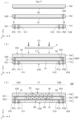
- FIG. 1 is an external perspective view of a resin substrate 101 according to a first preferred embodiment of the present invention.
- FIG. 2 is a front view of the resin substrate 101 .
- FIG. 3 is an exploded plan view of the resin substrate 101 .
- FIG. 4 is a cross-sectional view of a main portion of an electronic device 301 according to the first preferred embodiment of the present invention.
- FIG. 5 is a cross-sectional view showing steps for manufacturing a resin layer 13 a in a sequential order, the steps before the resin layer 13 a is laminated.
- FIG. 6 is a cross-sectional view showing steps for manufacturing the resin substrate 101 in a sequential order.
- FIG. 7 is an external perspective view of a resin substrate 102 according to a second preferred embodiment of the present invention.
- FIG. 8 is a front view of the resin substrate 102 .
- FIG. 9 is an exploded plan view of the resin substrate 102 .
- FIG. 10 is a cross-sectional view showing steps for manufacturing a resin layer 11 b in a sequential order, the steps before the resin layer 11 b is laminated.
- FIG. 11 is a cross-sectional view showing steps for manufacturing the resin substrate 102 in a sequential order.
- FIG. 12 A is an external perspective view of a resin substrate 103 according to a third preferred embodiment of the present invention
- FIG. 12 B is a cross-sectional view of the resin substrate 103 .
- FIG. 13 is an exploded plan view of the resin substrate 103 .
- FIG. 14 A is an external perspective view of a resin substrate 104 according to a fourth preferred embodiment of the present invention
- FIG. 14 B is a cross-sectional view of the resin substrate 104 .
- FIG. 15 is an exploded plan view of the resin substrate 104 .
- FIG. 16 is a front view of a resin substrate 104 A where a first section F 1 has been bent.
- FIG. 17 is a cross-sectional view showing steps for manufacturing the resin substrate 104 in a sequential order.
- FIG. 18 is a front view showing a main part of an electronic device 302 according to a fifth preferred embodiment of the present invention.
- FIG. 1 is an external perspective view of a resin substrate 101 according to a first preferred embodiment of the present invention.
- FIG. 2 is a front view of the resin substrate 101 .
- FIG. 3 is an exploded plan view of the resin substrate 101 .
- a signal line 40 is shown with a dot pattern.
- the resin substrate 101 includes an insulating base material 10 A, the signal line 40 , a ground conductor 51 , a ground conductor 52 , a ground conductor 53 , an interlayer connection conductor V 11 , an interlayer connection conductor V 12 , an interlayer connection conductor VG 1 , an interlayer connection conductor VG 2 , a mounting electrode P 11 , a mounting electrode P 12 , a ground electrodes PG 1 , a ground electrodes PG 2 , a protective layer 1 and others.
- the insulating base material 10 A is a resin (i.e., a thermoplastic resin) element having a cuboid shape, with its longitudinal direction aligned with an X-axis direction.
- the insulating base material 10 A includes a first main surface VS 1 and a second main surface VS 2 that oppose each other. Each of the first main surface VS 1 and the second main surface VS 2 is parallel or substantially parallel to the X-axis direction and a Y-axis direction.
- the second main surface VS 2 includes the mounting electrode P 11 , the mounting electrode P 12 , the ground conductor 51 , and the protective layer thereon.
- Each of the mounting electrode P 11 , the mounting electrode P 12 , the ground electrodes PG 1 , and the ground electrodes PG 2 is exposed on the second main surface VS 2 .
- the insulating base material 10 A includes the signal line 40 , the ground conductor 52 , the ground conductor 53 , and the interlayer connection conductors V 11 , V 12 , VG 1 , and VG 2 therein.
- the insulating base material 10 A is divided into a first section F 1 , a second section F 2 A, and a second section F 2 B.
- the first section F 1 includes at least a portion subjected to bending (as will be described later).
- the second section F 2 A, the first section F 1 , and the second section F 2 B are arranged in a positive X-axis direction in this sequential order.
- the first section F 1 includes a first region R 1 , a second region R 2 , and a third region R 3 .
- the first region R 1 is closest to the first main surface VS 1 .
- the second region R 2 is closest to the second main surface VS 2
- the third region R 3 is located between the first region R 1 and the second region R 2 .
- the insulating base material 10 A includes a plurality of resin layers, i.e., a resin layer 11 a , a resin layer 12 a , and a resin layer 13 a , each made of a resin (thermoplastic resin).
- the resin layers 11 a , 12 a , and 13 a are laminated in this sequential order to form the insulating base material 10 A.
- Each of the resin layers 11 a , 12 a , and 13 a is a rectangular or substantially rectangular flat plate, with its longitudinal direction aligned with the X-axis direction.
- Each of the resin layers 11 a , 12 a , and 13 a is, for example, a resin sheet including a photo-oriented polymer in addition to a liquid crystal polymer (LCP) or a polyimide (PI), for example.
- the photo-oriented polymer is preferably, for example, a vinyl cinnamate polymer, a chalcone polymer, an azo polymer, or a polyamide polymer.
- the resin layer 11 a includes, on its rear surface, the mounting electrode P 11 , the mounting electrode P 12 , and the ground conductor 51 .
- the mounting electrode P 11 is a conductor pattern having a rectangular or substantially rectangular shape and arranged near a first end of the resin layer 11 a (i.e., a left end of the resin layer 11 a in FIG. 3 ).
- the mounting electrode P 12 is a conductor pattern having a rectangular or substantially rectangular shape and arranged near a second end of the resin layer 11 a (i.e., a right end of the resin layer 11 a in FIG. 3 ).
- the ground conductor 51 is a conductor pattern having a rectangular or substantially rectangular shape and arranged over an entire or substantially an entire surface of the resin layer 11 a .
- Each of the mounting electrode P 11 , the mounting electrode P 12 , and the ground conductor 51 is the conductor pattern such as, for example, a Cu foil.
- the resin layer 11 a includes the interlayer connection conductors V 11 , the interlayer connection conductor V 12 , and the interlayer connection conductors VG 1 (provided in plural number) thereon.
- the resin layer 12 a includes, on its rear surface, the signal line 40 and the ground conductor 52 .
- the signal line 40 is a conductor pattern having a linear shape and extending in a transmission direction (i.e., the X-axis direction).
- the ground conductor 52 is a conductor pattern having a rectangular shape and arranged over an entire or substantially an entire surface of the resin layer 12 a .
- Each of the signal line 40 and the ground conductor 52 is a conductor pattern such as, for example, the Cu foil.
- the resin layer 12 a includes the interlayer connection conductors VG 2 (provided in plural number) thereon.
- the resin layer 13 a includes, on its rear surface, the ground conductor 53 .
- the ground conductor 53 is a conductor pattern having a rectangular or substantially rectangular shape and arranged over an entire or substantially entire surface of the resin layer 13 a .
- the ground conductor 53 is the conductor pattern such as, for example, the Cu foil.
- the protective layer 1 is a protective film laminated on the rear surface of the resin layer 11 a , and has the same or substantially the same planar shape as the resin layer 11 a .
- the protective layer 1 includes an opening OP 11 and an opening OP 12 positioned respectively in correspondence to the mounting electrode P 11 and the mounting electrode P 12 .
- the protective layer 1 includes openings OG 1 and openings OG 2 , each provided in plural number and positioned in correspondence to the ground conductor 51 .
- the protective layer 1 is a coverlay film, such as, for example, the polyimide (PI) or a polyethylene terephthalate (PET), or a solder resist film including, for example, an epoxy resin as a main component.
- PI polyimide
- PET polyethylene terephthalate
- solder resist film including, for example, an epoxy resin as a main component.
- the mounting electrode P 11 and the mounting electrode P 12 are electrically conductive. More specifically, the mounting electrode P 11 is connected to one end of the signal line 40 via the interlayer connection conductor V 11 .
- the mounting electrode P 12 is connected to the other end of the signal line 40 via the interlayer connection conductor V 12 .
- the ground conductor 51 (as the ground electrodes PG 1 and PG 2 ), the ground conductor 52 , and the ground conductor 53 are electrically conductive. More specifically, the ground conductor 51 is connected to the ground conductor 52 via the interlayer connection conductors VG 1 (provided in plural number), and the ground conductor 52 is connected to the ground conductor 53 via the interlayer connection conductors VG 2 (provided in plural number).
- the signal line 40 , the ground conductor 51 , the ground conductor 53 , the resin layer 11 a located between the signal line 40 and the ground conductor 51 , and the resin layer 12 a located between the signal line 40 and the ground conductor 53 are configured to define a transmission line (i.e., a strip-line transmission line).
- the first region R 1 has a greater degree of resin molecular orientation in the Y-axis direction than other areas (i.e., the second section F 2 A, the second section F 2 B, the second region R 2 and the third region R 3 ). Particularly, the first region R 1 has a greater degree of resin molecular orientation in the Y-axis direction than the second sections F 2 A and F 2 B.
- the resin molecular orientation in the X-axis direction and the resin molecular orientation in the Y-axis direction are isotropic.
- the degree of resin molecular orientation is determined as follows: azimuth ( ⁇ angle) in a certain region is measured by, for example, (wide angle) X-ray diffraction, and based on the azimuth and intensity distribution, each of the resin molecular orientation (nx) in the X-axis direction and the resin molecular orientation (ny) in the Y-axis direction is obtained.
- the resin molecules are oriented in the X-axis direction is defined as a case that satisfies a relationship: (ny/nx) ⁇ about 0.9 in the certain region; and “the resin molecules are oriented in the Y-axis direction” is defined as a case that satisfies a relationship: (nx/ny) ⁇ about 0.9 in the certain region.
- the resin molecules are oriented in neither the X-axis direction nor the Y-axis direction.
- the resin molecular orientation in the X-axis direction and that in the Y-axis direction are isotropic.
- first section corresponds to a region overlapping an area where the resin molecules are oriented in the X-axis direction or an area where the resin molecules are oriented in the Y-axis direction in, for example, a plan view (i.e., when viewed in the Z-axis direction); and the “second section” corresponds to the other regions.
- a boundary surface between the area where the resin molecules are oriented in the X-axis direction and the other areas is defined as, for example, a surface where the relationship (ny/nx) about 0.9 is changed to the relationship (ny/nx)>about 0.9.
- a boundary surface between the area where the resin molecules are oriented in the Y-axis direction and the other areas is defined as, for example, a surface where the relationship (nx/ny) about 0.9 is changed to the relationship (nx/ny)>about 0.9. Note that, in any one of the cases above, the boundary surface is included in the other areas (where the resin molecules are not oriented in the X-axis direction or in the Y-axis direction).
- the resin element When a resin element includes resin molecules oriented in the Y-axis direction, the resin element has a greater Young's modulus in the Y-axis direction than a resin element having isotropic resin molecular orientation, and the resin element is smaller in Young's modulus in the X-axis direction than the resin element having the isotropic resin molecular orientation, the X-axis direction orthogonal or substantially orthogonal to the Y-axis direction.
- the first region R 1 has a greater degree of resin molecular orientation in the Y-axis direction than the other areas (i.e., the second section F 2 A, the second section F 2 B, the second region R 2 , and the third region R 3 ).
- the first region R 1 has a greater degree of resin molecular orientation in the Y-axis direction than the second sections F 2 A and F 2 B.
- the first region R 1 has a greater Young's modulus in the Y-axis direction than the other areas, and the first region R 1 is smaller in Young's modulus in the X-axis direction than the other areas.
- the first region R 1 has a greater Young's modulus in the Y-axis direction than the second sections F 2 A and F 2 B, and the first region R 1 is smaller in Young's modulus in the X-axis direction than the second sections F 2 A and F 2 B.
- the first section F 1 when the first section F 1 is bent, tensile stress is applied to the first region R 1 in the X-axis direction, so that the first region R 1 is subjected to tensile deformation to a greater extent than the other areas.
- the first section F 1 is bent more easily in the X-axis direction than the second sections F 2 A and F 2 B.
- the resin element When a resin element has resin molecules oriented in the Y-axis direction, the resin element is smaller in linear expansion coefficient in the Y-axis direction than a resin element having the isotropic resin molecular orientation, and the resin element has a greater linear expansion coefficient in the X-axis direction than the resin element having the isotropic resin molecular orientation, the X-axis direction orthogonal or substantially orthogonal to the Y-axis direction.
- the first region R 1 has a greater linear expansion coefficient in the X-axis direction than the other areas (i.e., the second section F 2 A, the second section F 2 B, the second region R 2 and the third region R 3 ).
- the first region R 1 has a greater linear expansion coefficient in the X-axis direction than the second sections F 2 A and F 2 B.
- the first section F 1 is bent more easily in the X-axis direction than the second sections F 2 A and F 2 B in the insulating base material 10 A.
- the interlayer connection conductors V 11 , V 12 , VG 1 , and VG 2 are only in the second sections F 2 A and F 2 B.
- these interlayer connection conductors are in the first section F 1 (that is to be subjected to bending)
- the interlayer connection conductors V 11 , V 12 , VG 1 , and VG 2 are not in the first section F 1 .
- the interlayer connection conductors V 11 , V 12 , VG 1 , and VG 2 are less prone to being broken.
- the insulating base material 10 A includes the plurality of resin layers, i.e., the resin layers 11 a , 12 a , and 13 a , each made of the thermoplastic resin.
- the resin layers 11 a , 12 a , and 13 a have been laminated and heat-pressed (i.e., collectively pressed)
- the insulating base material 10 A is easily formed without an adhesive layer. Accordingly, the manufacturing steps of the resin substrate 101 are simplified, thus keeping costs low.
- the insulating base material 10 A as the thermoplastic resin element, the present preferred embodiment provides a resin substrate that is easily plastically deformed and that maintains (or retains) a desirable shape.
- FIG. 4 is a cross-sectional view of a main portion of an electronic device 301 according to the first preferred embodiment.
- the electronic device 301 includes a resin substrate 101 A, a circuit board 201 , and a circuit board 202 .
- the resin substrate 101 A includes a first section F 1 that has been bent (i.e., plastically deformed).
- the resin substrate 101 A includes an insulating base material 10 A, and the insulating base material 10 A includes a bent portion as the first section F 1 , the bent portion having been bent in the Z-axis direction.
- Other configurations of the resin substrate 101 A are the same or substantially the same as those of the resin substrate 101 .
- the bending of the first section F 1 of the insulating base material 10 A is performed in steps described below.
- the insulating base material 10 A is heated and bent with a mold or the like, and when the thermoplastic resin of the insulating base material 10 A has been cooled down and solidified, the mold or the like is removed such that the first section F 1 is maintained (or remained) bent.
- the insulating base material 10 A additionally includes a thermal cross-linking agent (e.g., epoxy resin), the first section F 1 of the insulating base material 10 A is bent into a desirable shape, and the insulating base material 10 A is heated such that the first section F 1 is maintained bent.
- a thermal cross-linking agent e.g., epoxy resin
- the circuit board 201 includes a first surface S 21
- the circuit board 202 includes a second surface S 22 .
- the first surface S 21 is parallel or substantially parallel to an X-Y plane
- the second surface S 22 is parallel or substantially parallel to a Y-Z plane.
- the first surface S 21 of the circuit board 201 includes an external electrode EP 11 and a ground electrode EG 1 thereon
- the second surface S 22 of the circuit board 202 includes an external electrode EP 12 and a ground electrode EG 2 thereon.
- the resin substrate 101 A is mounted on the circuit boards 201 and 202 , with the first section F 1 being bent.
- the resin substrate 101 A includes a mounting electrode P 11 that is to be connected to the external electrode EP 11 of the circuit board 201 with a conductive bonding material 5 , such as solder, for example.
- the resin substrate 101 A includes a ground electrode PG 1 that is to be connected to the ground electrode EG 1 of the circuit board 201 with the conductive bonding material 5 .
- the resin substrate 101 A includes a mounting electrode P 12 that is to be connected to the external electrode EP 12 of the circuit board 202 with the conductive bonding material 5 .
- the resin substrate 101 A further includes a ground electrode PG 2 that is to be connected to the ground electrode EG 2 of the circuit board 202 with the conductive bonding material 5 .
- the first section F 1 of the resin substrate 101 A is easily bent in the Z-axis direction.
- the resin substrate 101 A is easily mounted on the circuit boards 201 and 202 , each with its surface at different height in the Z-axis direction from the other.
- each of the second sections F 2 A and F 2 B the resin molecular orientation in the X-axis direction and the resin molecular orientation in the Y-axis direction are isotropic, and the second sections F 2 A and F 2 B respectively include the mounting electrodes P 11 and P 12 in the resin substrate 101 A.
- the resin substrate 101 A is mounted on the circuit boards 201 and 202 (e.g., when the resin substrate 101 A is mounted by hot bar soldering or is in a reflow step)
- each of the second sections F 2 A and F 2 B is less prone to being deformed. Accordingly, a bonding failure between the resin substrate 101 A and the circuit board 201 or the circuit board 202 is reduced or prevented.
- FIG. 5 is a cross-sectional view showing steps for manufacturing the resin layer 13 a in a sequential order, the steps before the resin layer 13 a is laminated.
- FIG. 6 is a cross-sectional view showing the steps for manufacturing the resin substrate 101 in a sequential order.
- FIG. 5 shows the resin layer 13 a only.
- FIGS. 5 and 6 show steps for manufacturing a “single chip (i.e., single piece)”, but in actual manufacturing steps of the resin substrate 101 , an aggregate substrate is used.
- the “aggregate substrate” corresponds to a mother substrate including a plurality of the resin substrates 101 . The same applies to the subsequent drawings, each showing the corresponding manufacturing steps.
- the resin layer 13 a formed of the resin is prepared.
- the resin layer 13 a is, for example, the resin sheet including the photo-oriented polymer in addition to the liquid crystal polymer (LCP) or the polyimide (PI). While not shown, the same applies to each of the resin layers 11 a and 12 a.
- an area that is to be the first region of the insulating base material i.e., an area near a center of the resin layer 13 a in the X-axis direction as shown in (1), (2) and (3) of FIG. 5
- the light LC is polarized in the Y-axis direction by a polarizing plate 3 to be light LY; and the resin layer 13 a is irradiated with the light LY (that has been polarized), so that the resin molecules in the area irradiated are oriented in the Y-axis direction.
- the resin molecules in the area that is to be the first region
- the resin molecules in the area are oriented in the Y-axis direction.
- the area (that is to be the first region of the insulating base material) is irradiated with light or laser, so that the resin molecules in the area are oriented in the Y-axis direction.
- a sequence of these steps corresponds to an example of a “first molecular orientation step”.
- the ground conductor 53 is arranged on the rear surface of the resin layer 13 a . More specifically, on the rear surface of the resin layer 13 a , a metal foil is laminated and patterned by photolithography such that the ground conductor 53 is arranged on the rear surface of the resin layer 13 a.
- the resin layer 11 a includes the mounting electrode P 11 , the mounting electrode P 12 , the ground conductor 51 , the interlayer connection conductor V 11 , the interlayer connection conductor V 12 , the interlayer connection conductors VG 1 , and others thereon
- the resin layer 12 a includes the signal line 41 , the ground conductor 52 , the interlayer connection conductors VG 2 , and others thereon.
- the interlayer connection conductors are arranged, for example, as follows.
- Each of the resin layers includes a hole formed by laser irradiation, drilling, or the like, the hole is filled with a conductive paste including a metal powder, e.g., Cu, Sn, or an alloy thereof, and a resin material, and the resin layers are to be heat-pressed such that the conductive paste is solidified.
- a conductive paste including a metal powder, e.g., Cu, Sn, or an alloy thereof, and a resin material, and the resin layers are to be heat-pressed such that the conductive paste is solidified.
- the resin layers 11 a , 12 a , and 13 a are heat-pressed to form the insulating base material 10 A as shown in (2) of FIG. 6 .
- the first region R 1 has a greater degree of resin molecular orientation in the Y-axis direction than the second region R 2 , the third region R 3 , the second section F 2 A, and the second section F 2 B.
- the first region R 1 has a greater degree of resin molecular orientation in the Y-axis direction than the second sections F 2 A and F 2 B.
- a sequence of these steps corresponds to an example of a “first insulating base material formation step”.
- the protective layer 1 is arranged on the second main surface VS 2 of the insulating base material 10 A, resulting in the resin substrate 101 as shown in (3) of FIG. 6 .
- the protective layer 1 is a coverlay film, such as, for example, the polyimide (PI) or a polyethylene terephthalate (PET), or a solder resist film containing, for example, an epoxy resin as a main component.
- the resin substrate 101 having the following advantageous feature is easily manufactured. Even when the first section F 1 of the insulating base material 10 A is bent, each of the second sections F 2 A and F 2 B is less prone to being deformed or bent.
- the resin substrate 101 is easily formed. Accordingly, the manufacturing steps of the resin substrate 101 are simplified, thus keeping costs low.
- the resin molecules are oriented. Accordingly, compared with a case where the resin layers 11 a , 12 a , and 13 a are laminated to form an insulating base material and then resin molecules are oriented in the insulating material, the first region may be designed to have a wider range of degree of resin molecular orientation.
- FIG. 7 is an external perspective view of a resin substrate 102 according to the second preferred embodiment.
- FIG. 8 is a front view of the resin substrate 102 .
- FIG. 9 is an exploded plan view of the resin substrate 102 . In FIG. 9 , for ease of understanding of the structure, a signal line 40 is shown with a dot pattern.
- the resin substrate 102 includes an insulating base material 10 B.
- Other configurations of the resin substrate 102 are the same or substantially the same as those of the resin substrate 101 .
- the resin substrate 102 is different from the resin substrate 101 according to the first preferred embodiment, as described below.
- the insulating base material 10 B includes a plurality of resin layers. i.e., a resin layer 11 b , a resin layer 12 b , and a resin layer 13 b , each made of a resin (for example, thermoplastic resin).
- the resin layers 11 b , 12 b , and 13 b are laminated in this sequential order to define the insulating base material 10 B.
- the resin layers 11 b , 12 b , and 13 b respectively have the same or substantially the same configurations as those of the resin layers 11 a , 12 a , and 13 a described in the first preferred embodiment.
- a second region R 2 has a greater degree of resin molecular orientation in an X-axis direction than the other areas (i.e., a second section F 2 A, a second section F 2 B, a first region R 1 , and a third region R 3 ).
- the second region R 2 has a greater degree of resin molecular orientation in the X-axis direction than the second sections F 2 A and F 2 B.
- the second region R 2 has a greater Young's modulus in the X-axis direction than the other areas, and the second region R 2 is smaller in Young's modulus in a Y-axis direction than the other areas.
- the second region R 2 has a greater Young's modulus in the X-axis direction than the second sections F 2 A and F 2 B, and the second region R 2 is smaller in Young's modulus in the Y-axis direction than the second sections F 2 A and F 2 B.
- the resin molecular orientation in the X-axis direction and the resin molecular orientation in the Y-axis direction are isotropic.
- FIG. 10 is a cross-sectional view showing steps for manufacturing the resin layer 11 b in a sequential order, the steps before the resin layer 11 b is laminated.
- FIG. 11 is a cross-sectional view showing steps for manufacturing the resin substrate 102 in a sequential order. Note that, for convenience of description, FIG. 10 shows the resin layer 11 b only.
- the area (that is to be the second region of the insulating base material) is irradiated with light or a laser, so that the resin molecules in the area are oriented in the X-axis direction.
- a sequence of these steps corresponds to an example of a “second molecular orientation step”.
- a mounting electrode P 11 , a mounting electrode P 12 , and a ground conductor 51 are provided on a rear surface of the resin layer 11 b . More specifically, on the rear surface of the resin layer 11 b , a metal foil is laminated and patterned by photolithography such that the mounting electrode P 11 , the mounting electrode P 12 , and the ground conductor 51 are provided on the rear surface of the resin layer 11 b.
- the plurality of resin layers i.e., the resin layers 11 b , 12 b , and 13 b are laminated in this sequential order.
- the resin layer 12 b includes a signal line 41 , a ground conductor 52 , interlayer connection conductors VG 2 , and others thereon
- the resin layer 13 b includes a ground conductor 53 thereon.
- the resin layers 11 b , 12 b , and 13 b are heat-pressed to form the insulating base material 10 B as shown in (2) of FIG. 11 .
- the second region R 2 has a greater degree of resin molecular orientation in the X-axis direction than the first region R 1 , the third region R 3 , the second section F 2 A, and the second section F 2 B.
- the second region R 2 has a greater degree of resin molecular orientation in the X-axis direction than the second sections F 2 A and F 2 B.
- a sequence of these steps corresponds to an example of a “first insulating base material formation step”.
- a protective layer 1 is provided on a second main surface VS 2 of the insulating base material 10 B, resulting in the resin substrate 102 as shown in (3) of FIG. 11 .
- the resin substrate 102 having the following advantageous feature is easily manufactured.
- the insulating base material 10 B even when the first section F 1 is bent, each of the second sections F 2 A and F 2 B is less prone to being deformed or bent.
- a resin substrate which includes a resin layer having resin molecules oriented in the Y-axis direction and a resin layer having resin molecules oriented in the X-axis direction, will be described.
- FIG. 12 A is an external perspective view of a resin substrate 103 according to the third preferred embodiment
- FIG. 12 B is a cross-sectional view of the resin substrate 103
- FIG. 13 is an exploded plan view of the resin substrate 103 .
- each of a signal line 41 and a signal line 42 is shown with a dot pattern.
- the resin substrate 103 includes an insulating base material 10 C, two signal lines, i.e., the signal lines 41 and 42 , a protective layer 2 , and others.
- Other configurations of the resin substrate 103 are the same or substantially the same as those of the resin substrate 101 .
- the resin substrate 103 is different from the resin substrate 101 according to the first preferred embodiment, as described below.
- the insulating base material 10 C includes a plurality of resin layers, i.e., a resin layer 11 c , a resin layer 12 c , and a resin layer 13 c , each made of a resin (for example, thermoplastic resin).
- the resin layers 11 c , 12 c , and 13 c are laminated in this sequential order to form the insulating base material 10 C.
- Each of the resin layers 11 c and 13 c is preferably, for example, a resin sheet including a photo-oriented polymer, in addition to a liquid crystal polymer (LCP) or a polyimide (PI).
- the resin layer 12 c is preferably, for example, a resin sheet including the liquid crystal polymer (LCP) or the polyimide (PI) as a main component.
- the resin layer 11 c includes, on its rear surface, a mounting electrode P 11 , a mounting electrode P 12 , a mounting electrode P 21 , a mounting electrode P 22 , and a ground conductor 51 .
- Each of the mounting electrodes P 11 and P 21 is a conductor pattern having a rectangular or substantially rectangular shape and provided adjacent to or in the vicinity of a first end of the resin layer 11 c (i.e., a left end of the resin layer 11 c in FIG. 13 ).
- the mounting electrodes P 11 and P 21 are arranged in the Y-axis direction.
- Each of the mounting electrodes P 12 and P 22 is a conductor pattern having a rectangular or substantially rectangular shape and provided adjacent to or in the vicinity of a second end of the resin layer 11 c (i.e., a right end of the resin layer 11 c in FIG. 13 ).
- the mounting electrodes P 12 and P 22 are arranged in the Y-axis direction.
- the ground conductor 51 is a conductor pattern having a rectangular or substantially rectangular shape and provided over an entire or substantially an entire surface of the resin layer 11 c .
- the resin layer 11 c includes interlayer connection conductors V 11 , V 14 , V 21 , V 24 , and VG 1 thereon.
- the resin layer 12 c includes, on its surface, the signal line 41 , the signal line 42 , and a ground conductor 52 .
- Each of the signal lines 41 and 42 is a conductor pattern having a linear shape and extending in a transmission direction (i.e., the X-axis direction).
- the signal lines 41 and 42 are arranged in the Y-axis direction and are parallel or substantially parallel to each other.
- the ground conductor 52 is a conductor pattern having a rectangular or substantially rectangular shape and provided over an entire or substantially an entire surface of the resin layer 12 c .
- the resin layer 12 c includes interlayer connection conductors V 12 , V 13 , V 22 , V 23 , and VG 2 thereon.
- the resin layer 13 c includes, on its surface, a ground conductor 53 .
- the ground conductor 53 is a conductor pattern having a rectangular or substantially rectangular shape and provided over an entire or substantially entire surface of the resin layer 13 c .
- the resin layer 13 c includes interlayer connection conductors VG 3 thereon.
- a protective layer 1 is a protective film laminated on the rear surface of the resin layer 11 c , and has the same or substantially the same planar shape as the resin layer 11 c .
- the protective layer 1 includes an opening OP 11 , an opening OP 12 , an opening OP 21 , and an opening OP 22 that are respectively positioned in correspondence to the mounting electrode P 11 , the mounting electrode P 12 , the mounting electrode P 21 , and the mounting electrode P 22 .
- the protective layer 1 includes openings OG 1 and openings OG 2 , each provided in plural number and positioned in correspondence to the ground conductor 51 .
- the portion of the ground conductor 51 exposed from the opening OG 1 corresponds to each of the “ground electrodes PG 1 ”, and the portion of the ground conductor 51 exposed from the opening OG 2 corresponds to each of the “ground electrodes PG 2 ”.
- the protective layer 2 is a protective film laminated on the surface of the resin layer 13 c , and has the same or substantially the same planar shape as the resin layer 13 c.
- the mounting electrode P 11 and the mounting electrode P 12 are electrically conductive. More specifically, the mounting electrode P 11 is connected to one end of the signal line 41 via the interlayer connection conductors V 11 and V 12 .
- the mounting electrode P 12 is connected to the other end of the signal line 41 via the interlayer connection conductors V 13 and V 14 .
- the mounting electrode P 21 and the mounting electrode P 22 are electrically conductive. More specifically, the mounting electrode P 21 is connected to one end of the signal line 42 via the interlayer connection conductors V 21 and V 22 .
- the mounting electrode P 22 is connected to the other end of the signal line 42 via the interlayer connection conductors V 23 and V 24 .
- the ground conductor 51 (as the ground electrodes PG 1 and PG 2 ), the ground conductor 52 , and the ground conductor 53 are electrically connected. More specifically, the ground conductor 51 is connected to the ground conductor 52 via the interlayer connection conductors VG 1 (provided in plural number) and the interlayer connection conductors VG 2 (provided in plural number). The ground conductor is connected to the ground conductor 53 via the interlayer connection conductors VG 3 (provided in plural number).
- the signal line 41 , the ground conductor 51 , the ground conductor 53 , the resin layer 11 c located between the signal line 41 and the ground conductor 51 , the resin layer 12 c located between the signal line 41 and the ground conductor 51 , and the resin layer 13 c located between the signal line 41 and the ground conductor 53 are configured to define a transmission line (i.e., a strip-line transmission line).
- the signal line 42 , the ground conductor 51 , the ground conductor 53 , the resin layer 11 c located between the signal line 42 and the ground conductor 51 , the resin layer 12 c located between the signal line 42 and the ground conductor 51 , and the resin layer 13 c located between the signal line 42 and the ground conductor 53 are configured to define a transmission line (i.e., strip-line transmission line).
- a first region R 1 has a greater degree of resin molecular orientation in the Y-axis direction than the other areas (i.e., a second section F 2 A, a second section F 2 B, a second region R 2 , and a third region R 3 ).
- the first region R 1 has a greater degree of resin molecular orientation in the Y-axis direction than the second sections F 2 A and F 2 B.
- the second region R 2 has a greater degree of resin molecular orientation in the X-axis direction than the other areas (i.e., the second section F 2 A, the second section F 2 B, the first region R 1 , and the third region R 3 ).
- the second region R 2 has a greater degree of resin molecular orientation in the X-axis direction than the second sections F 2 A and F 2 B. Note that, in each of the second sections F 2 A and F 2 B, the resin molecular orientation in the X-axis direction and the resin molecular orientation in the Y-axis direction are isotropic.
- each of the resin layers 11 c and 13 c includes the photo-oriented polymer, but the resin layers 12 c does not include the photo-oriented polymer.
- a resin including a photo-oriented polymer has a greater dielectric constant than a resin including no photo-oriented polymer.
- the third region R 3 (i.e., the resin layer 12 c ) has a dielectric constant ( ⁇ 3 ) smaller than a dielectric constant ( ⁇ 1 ) of the first region R 1 (i.e., the resin layer 13 c ) and smaller than a dielectric constant ( ⁇ 2 ) of the second region R 2 (i.e., the resin layer 11 c ), in other words, ⁇ 3 ⁇ 1 , and ⁇ 3 ⁇ 2 .
- each of the signal lines 41 and 42 is located in (is in contact with) the third region R 3 that has excellent high-frequency characteristics (i.e., has a small dielectric loss tangent tan ⁇ ).
- the resin substrate has an improved high-frequency characteristic.
- the resin substrate 103 compared with an insulating base material including only a plurality of resin layers including the photo-oriented polymer, the resin substrate 103 has less conductor loss in circuits or the resin substrate 103 (i.e., the insulating base material 10 C) is reduced in thickness.
- a linear width of each of the conductor patterns is increased, thus reducing the conductor loss in the circuit.
- the resin substrate includes a circuit having a predetermined characteristic, it is possible, without reducing the linear widths of the conductor patterns, to reduce a width of each of the resin layers, thus reducing the thickness of the insulating base material 10 C.
- At least a portion of the ground conductor 51 and at least a portion of the ground conductor 52 may be respectively provided in the first region R 1 and the second region R 2 both of which have a greater dielectric constant.
- Each of the ground conductors is not configured to transmit a high-frequency signal.
- an influence on the high-frequency characteristic of the resin substrate is limited, compared with a case where each of the signal lines is provided in the region with a greater dielectric constant.
- an insulating base material may include a plurality of resin layers, not all of which include a photo-oriented polymer.
- a resin substrate according to preferred embodiments of the present invention may include an insulating base material including a plurality of resin layers, only some of which include the photo-oriented polymer.
- FIG. 14 A is an external perspective view of a resin substrate 104 according to a fourth preferred embodiment
- FIG. 14 B is a cross-sectional view of the resin substrate 104
- FIG. 15 is an exploded plan view of the resin substrate 104 .
- each of a signal line 41 and a signal line 42 is shown with a dot pattern.
- the resin substrate 104 includes an insulating base material 10 D and two signal lines, i.e., the signal line 41 and the signal line 42 . Further, unlike the resin substrate 101 , the resin substrate 104 does not include a protective layer. Other configurations of the resin substrate 104 are the same or substantially the same as those of the resin substrate 101 .
- the resin substrate 103 is different from the resin substrate 101 according to the first preferred embodiment, as described below.
- the insulating base material 10 D includes a plurality of resin layers. i.e., a resin layer 11 d , a resin layer 12 d , and a resin layer 13 d , each made of a resin (for example, thermosetting resin).
- the resin layers 11 d , 12 d , and 13 d are laminated in this sequential order to define the insulating base material 10 D.
- Each of the resin layers 11 d , 12 d , and 13 d is preferably, for example, a resin sheet including a photo-oriented polymer, in addition to an epoxy resin (EP).
- the resin layer 11 d includes, on its rear surface, a mounting electrode P 11 , a mounting electrode P 12 , a mounting electrode P 21 , and a mounting electrode P 22 .
- Each of the mounting electrodes P 11 and P 21 is a conductor pattern have a rectangular or substantially rectangular shape and provided adjacent to or in the vicinity of a first end of the resin layer 11 d (i.e., a left end of the resin layer 11 d in FIG. 15 ).
- the mounting electrodes P 11 and P 12 are arranged in an X-axis direction.
- Each of the mounting electrodes P 12 and P 22 is a conductor pattern having a rectangular or substantially rectangular shape and provided adjacent to or in the vicinity of a second end of the resin layer 11 d (i.e., a right end of the resin layer 11 d in FIG. 15 ).
- the resin layer 11 d includes interlayer connection conductors V 11 , V 12 , V 21 , and V 24 thereon.
- the resin layer 12 d includes, on its rear surface, the signal line 41 , a conductor 31 , and a conductor 32 .
- the signal line 41 is a conductor pattern having a linear shape and extends in a transmission direction (i.e., the X-axis direction).
- the conductor 31 is a conductor pattern having a rectangular or substantially rectangular shape and provided adjacent to or in the vicinity of a first end of the resin layer 12 d (i.e., a left end of the resin layer 12 d in FIG. 15 ).
- the conductor 32 is a conductor pattern having a rectangular or substantially rectangular shape and provided adjacent to or in the vicinity of a second end of the resin layer 12 d (a right end of the resin layer 12 d in FIG. 15 ).
- Each of the conductors 31 and 32 is preferably a Cu foil, for example.
- the resin layer 12 d includes an interlayer connection conductor V 22 and an interlayer connection conductor V 23 thereon.
- the resin layer 13 d includes, on its rear surface, the signal line 42 .
- the signal line 42 is a conductor pattern having a linear shape and extends in a transmission direction (i.e., the X-axis direction).
- a protective layer 1 is a protective film laminated on the rear surface of the resin layer 11 c , and has the same or substantially the same planar shape as the resin layer 11 c .
- the protective layer 1 includes an opening OP 11 , an opening OP 12 , an opening OP 21 , and an opening OP 22 that are respectively positioned in correspondence to the mounting electrode P 11 , the mounting electrode P 12 , the mounting electrode P 21 , and the mounting electrode P 22 .
- the protective layer 1 includes openings OG 1 and openings OG 2 , each provided in plural number and positioned in correspondence to the ground conductor 51 .
- the portion of the ground conductor 51 exposed from the opening OG 1 corresponds to each of the “ground electrodes PG 1 ”, and the portion of the ground conductor 51 exposed from the opening OG 2 corresponds to each of the “ground electrodes PG 2 ”.
- the protective layer 2 is a protective film laminated on the surface of the resin layer 13 c , and has the same or substantially the same planar shape as the resin layer 13 c.
- a first region R 1 has a greater degree of resin molecular orientation in the Y-axis direction than the other areas (i.e., a second section F 2 A, a second section F 2 B, a second region R 2 , and a third region R 3 ).
- the first region R 1 has a greater degree of resin molecular orientation in the Y-axis direction than the second sections F 2 A and F 2 B.
- the third region R 3 has a greater degree of resin molecular orientation in the Y-axis direction than the other areas (i.e., the second section F 2 A, the second section F 2 B, and the second region R 2 ).
- a first section F 1 has continuous changes (or has a gradual decrease) in degree of resin molecular orientation in the Y-axis direction from a first main surface VS 1 toward the second main surface VS 2 .
- the resin substrate 104 achieves the same or substantially the same advantageous operations and effects as the resin substrate 101 , that is, even when the first section F 1 is bent, each of the second sections F 2 A and F 2 B is less prone to being deformed or bent.
- the resin substrate 104 may not necessarily include the protective layer on the first main surface VS 1 or the second main surface VS 2 of the insulating base material.
- FIG. 16 is a front view of a resin substrate 104 A where a first section F 1 has been bent.
- the resin substrate 104 A includes an insulating base material 10 D, and the insulating base material 10 D includes a bent portion as the first section F 1 that has been bent into a U shape.
- the first section F 1 has a gradual decrease in linear expansion coefficient in the X-axis direction from the first main surface VS 1 toward to the second main surface VS 2 .
- the first section F 1 is automatically deformed as shown in FIG. 16 .
- the insulating base material 10 D is preferably, for example, a thermosetting resin element. Accordingly, when heated at the high temperature (that is higher than the temperature at which the resin layers are laminated), the insulating base material 10 D is cured, so that the first section F 1 is maintained bent.
- FIG. 17 is a cross-sectional view showing the steps for manufacturing the resin substrate 104 in a sequential order.
- the resin layers 11 d , 12 d , and 13 d are prepared.
- Each of the resin layers 11 d , 12 d , and 13 d is, for example, a resin sheet including a photo-oriented polymer in addition to a liquid crystal polymer (LCP) or a polyimide (PI).
- LCP liquid crystal polymer
- PI polyimide
- the mounting electrodes P 11 , P 12 , P 21 , and P 22 are provided on the rear surface of the resin layer 11 d
- the signal line 41 , the conductors 31 and 32 are provided on the rear surface of the resin layer 12 d
- the signal line 42 is provided on the rear surface of the resin layer 13 d .
- a metal foil is laminated and patterned by photolithography on the rear surface of each of the resin layers 11 d , 12 d , and 13 d .
- each of the mounting electrodes P 11 , P 12 , P 21 , and P 22 , each of the signal lines 41 and 42 , and each of the conductors 31 and 32 is provided on the rear surface of a corresponding one of the resin layers 11 d , 12 d , and 13 d.
- the resin layer 11 d includes the interlayer connection conductors V 11 , V 12 , V 21 , and V 24 thereon, and the resin layer 12 d includes the interlayer connection conductors V 22 and V 23 thereon.
- These interlayer connection conductors are provided, for example, as follows.
- Each of the resin layers includes a hole formed by laser irradiation, drilling, or the like, for example, the hole is filled with a conductive paste including a metal powder, e.g., Cu, Sn, or an alloy thereof, and a resin material, and the resin layers are to be heat-pressed such that the conductive paste is solidified.
- the plurality of resin layers i.e., the resin layers 11 d , 12 d , and 13 d , are laminated in this sequential order, and the resin layers 11 d , 12 d , and 13 d are heat-pressed to form an insulating base material 10 DP, as shown in (2) of FIG. 17 .
- a sequence of these steps to form the insulating base material 10 DP corresponds to an example of a “second insulating base material formation step”.
- an area that is to be the first region of the insulating base material is irradiated with light LC from the first main surface VS 1 , so that the resin molecules are oriented in the Y-axis direction.
- the light LC is polarized in the Y-axis direction by a polarizing plate 4 to be light LY, and a predetermined area of the insulating base material 10 DP is irradiated with the light LY (that has been polarized), so that the resin molecules in the predetermined area irradiated are oriented in the Y-axis direction.
- the insulating base material 10 D where, due to a light intensity distribution or a temperature distribution, the degree of resin molecular orientation in the Y-axis direction gradually decreases as a distance from the area irradiated with the light LY increases.
- the first section F 1 has continuous changes (or has the gradual decrease) in degree of resin molecular orientation in the Y-axis direction from the first main surface VS 1 toward the second main surface VS 2 .
- the first section F 1 has continuous changes (has a gradual decrease) in degree of resin molecular orientation in the Y-axis direction from an area near a center of the first section F 1 in planar direction (e.g., the X-axis direction) toward the second section F 2 A and the second section F 2 B.
- the area (that is to be the first region) is irradiated with light or laser from the first main surface VS 1 , so that the resin molecules in the first region are oriented in the Y-axis direction.
- a sequence of these steps corresponds to an example of a “third molecular orientation step”.
- the plurality of resin layers i.e., the resin layers 11 d , 12 d , and 13 d
- the manufacturing steps are simplified, thus keeping costs low.
- the present preferred embodiment provides the insulating base material 10 DP where the resin molecules are oriented.
- the present invention is not limited thereto.
- the resin molecules may be oriented in each of the plurality of resin layers before being laminated such that a resin substrate having the following feature is formed.
- the degree of resin molecular orientation changes in a sequential order from the first region R 1 through the third region R 3 to the second region R 2 .
- the present preferred embodiment provides an example of the resin substrate where the first section F 1 has the continuous changes (gradual decrease) in degree of resin molecular orientation in the Y-axis direction from the first main surface VS 1 toward the second main surface VS 2 .
- the present invention is not limited thereto.
- the first section F 1 may have continuous changes (or have a gradual decrease) in degree of resin molecular orientation in the X-axis direction from the second main surface VS 2 toward the first main surface VS 1 . It is possible to form a resin substrate of this type, for example, in steps described below.
- an area (that is to be the second region of the insulating base material) is irradiated with light polarized from the second main surface VS 2 , so that the resin molecules in the area are oriented in the X-axis direction.
- a sequence of these steps corresponds to an example of a “fourth molecular orientation step”.
- FIG. 18 is a front view showing a main portion of an electronic device 302 according to the fifth preferred embodiment.
- the electronic device 302 includes a resin substrate 105 A, a circuit board 201 , and a circuit board 202 .
- the circuit boards 201 and 202 respectively have the same or substantially the same configurations as those of the circuit boards 201 and 202 described in the first preferred embodiment.
- the circuit board 201 includes a first surface S 21
- the circuit board 202 includes a second surface S 22 .
- the first surface S 21 and the second surface S 22 are positioned parallel or substantially parallel to an X-Y plane and at different heights from each other in a Z-axis direction.
- the resin substrate 105 A includes an insulating base material 10 E that is divided into a first section F 1 , a second section F 2 A, a second section F 2 B, and a third section F 3 . Each of the first section F 1 and the third section F 3 is subjected to bending. In the insulating base material 10 E, the second section F 2 A, the first section F 1 , the third section F 3 , and the second section F 2 B are arranged in this sequential order.
- the resin substrate 105 A is mounted on the circuit boards 201 and 202 . More specifically, the resin substrate 105 A includes a mounting electrode P 11 that is to be connected to an external electrode EP 11 of the circuit board 201 with a conductive bonding material 5 .
- the resin substrate 105 A includes a mounting electrode P 12 that is to be connected to an external electrode EP 12 of the circuit board 202 with the conductive bonding material 5 .
- the resin substrate 105 A further includes a ground electrode that is to be connected to a ground electrode of each of the circuit boards 201 and 202 with the conductive bonding material 5 .
- the first section F 1 includes a first region R 1 A, a second region R 2 A, and a third region R 3 A.
- the third section F 3 includes a first region R 1 B, a second region R 2 B, and a third region R 3 B.
- the first region R 1 B is positioned closest to a first main surface VS 1 .
- the second region R 2 B is positioned closest to a second main surface VS 2 , and the third region R 3 B is located between the first region R 1 B and the second region R 2 B.
- the first section F 1 includes the first region R 1 A where resin molecules are oriented in a Y-axis direction
- the third section F 3 includes the second region R 2 B where the resin molecules are oriented in the Y-axis direction.
- the first section F 1 includes the second region R 2 A where the resin molecules are oriented in an X-axis direction
- the third section F 3 includes the first region R 1 B where the resin molecules are oriented in the X-axis direction.
- the third section F 3 includes the second region R 2 B that has a greater degree of resin molecular orientation in the Y-axis direction than the second sections F 2 A and F 2 B.
- the third section F 3 includes the first region R 1 B that has a greater degree of resin molecular orientation in the X-axis direction than the second sections F 2 A and F 2 B.
- the first section F 1 and the third section F 3 have the resin molecular orientations that are reverse to each other from the first regions toward the second regions (i.e., from the first main surface VS 1 toward the second main surface VS 2 ).
- the first section F 1 of the resin substrate 105 A is bent such that the first region R 1 A is tension-deformed and the second region R 2 A is compressively deformed.
- the first section F 1 is bent outward (i.e., having the second main surface VS 2 positioned at an inner peripheral side), as shown in FIG. 18 .
- the third section F 3 of the resin substrate 105 A is bent such that the second region R 2 B is tension-deformed and the first region R 1 B is compressively deformed.
- the third section F 3 is bent inward (i.e., having the first main surface VS 1 positioned at the inner peripheral side), as shown in FIG. 18 .
- the resin substrate 105 A is bent into a crank shape.
- the resin substrate when the resin substrate includes a portion that is to be bent in a direction reverse to that of the first section F 1 , the resin substrate may further include the third section F 3 .
- the shape thereof is not limited to an L-shape or the crank shape, and the shape may be changed or modified as appropriate within the technical range of the present invention.
- the third section F 3 includes the first region R 1 B that has a greater degree of resin molecular orientation in the X-axis direction, and includes the second region R 2 B that has a greater degree of resin molecular orientation in the Y-axis direction.
- the present invention is not limited thereto.
- the third section F 3 includes the first region R 1 B where the resin molecules are oriented in the X-axis direction, and includes the second region R 2 B where the resin molecules are oriented in the Y-axis direction.
- the present invention is not limited thereto.
- the resin molecular orientation may be in a reverse order of the resin molecular orientation in the first section F 1 (that has been described in each of the first, second, third, and fourth preferred embodiments).
- the first section F 1 of the present preferred embodiment may be replaced with, for example, the first section F 1 that has been described in each of the first to fourth preferred embodiments.
- the resin substrate corresponds to a cable to connect two circuit boards, but the present invention is not limited thereto.
- a resin substrate according to a preferred embodiment of the present invention may be, for example, an electronic component that is to be surface-mounted to a single circuit board.
- a second section (as a connector section) may include a connector as needed.
- the insulating base material preferably has a cuboid shape, with its longitudinal direction aligned with the X-axis direction.
- the shape is not limited thereto.
- the shape of the insulating base material may be changed or modified as appropriate within the technical range of the present invention, and may have the longitudinal direction not necessarily aligned with the X-axis direction.
- the insulating base material may have an L-shape, a U-shape, a crank shape, a T-shape, or a Y-shape planar shape.
- the insulating base material is divided into the second section, the first section, and the second section in this sequential order (or the insulating base material is divided into the second section, the first section, the third section, and the second section in this sequential order).
- an insulating base material according to preferred embodiments of the present invention is not limited thereto.
- the number of each of the first section, the second section, and the third section may be changed or modified as appropriate within the technical range of the present invention.
- the insulating base material may be divided into, for example, the second section, the first section, the second section, the first section, and the second section in this sequential order.
- the insulating base material includes the three resin layers laminated on each other.
- an insulating base material according to a preferred embodiment the present invention is not limited thereto.
- the number of the resin layers may be changed or modified as appropriate within the technical range of the present invention.
- the insulating base material may include, for example, a single, two, four or more resin layer(s).
- the three resin layers may not necessarily correspond respectively to the first region, the second region, and the third region.
- the plurality of resin layers have the same or substantially the same thickness.
- the thickness of each of the resin layers may be different from the other(s).
- the degree of resin molecular orientation in each of the regions corresponds to a degree of resin molecular orientation in an entire or substantially and entire portion of the corresponding region, and corresponds not to a degree of resin molecular orientation in only a portion of the corresponding region (e.g., a specific resin layer of the plurality of resin layers).
- the insulating base material is a thermoplastic resin element.
- an insulating base material is not limited thereto.
- the insulating base material may be a thermosetting resin element, for example.
- the insulating base material may be a laminated composite including a plurality of resin layers.
- the plurality of resin layers may not necessarily be heat-pressed (i.e., collectively pressed) to be surface attached to each other.
- the plurality of resin layers may alternatively have an adhesive layer therebetween.
- the circuit configurations on the resin substrate in each of the foregoing preferred embodiments are not restrictive, but may be changed or modified as appropriate within the technical range of the present invention.
- the resin substrate may include a circuit including, for example, a conductor pattern coil, a capacitor including a conductor pattern, or a frequency filter such as various filters (e.g., a low pass filter, a high pass filter, a band pass filter, or a band elimination filter).
- the resin substrate may include various other transmission lines (e.g., a microstrip line or a coplanar line).
- the resin substrate may have various electronic components, e.g., a chip component, mounted thereon or embedded therein.
- the resin substrate includes one or two transmission line(s).
- the present invention is not limited thereto.
- the number of transmission lines may be changed or modified as appropriate by circuit configuration on the resin substrate.
- the insulating base material includes the mounting electrodes having a rectangular or substantially rectangular shape on the second main surface VS 2 .
- the mounting electrodes are not limited thereto.
- Each of the mounting electrodes may have the shape, the number, and the position thereof changed or modified as appropriate within the technical range of the present invention.
- Each of the mounting electrodes may have the planar shape may be, for example, a polygonal shape, a circular shape, an elliptical shape, a circular-arc shape, a ring shape an L-shape, a U-shape, a T-shape, a Y-shape, a crank shape, or others.
- the insulating base material may include the mounting electrodes on each of the first main surface VS 1 and the second main surface VS 2 .
- the dielectric constant ( ⁇ 3 ) may be smaller than at least one of the dielectric constant ( ⁇ 1 ) and the dielectric constant ( ⁇ 2 ).
- At least one of the first main surface VS 1 and the second main surface VS 2 may be a surface parallel or substantially parallel to the X-axis direction and a Y-axis direction.
Landscapes
- Engineering & Computer Science (AREA)
- Microelectronics & Electronic Packaging (AREA)
- Manufacturing & Machinery (AREA)
- Production Of Multi-Layered Print Wiring Board (AREA)
- Laminated Bodies (AREA)
- Structure Of Printed Boards (AREA)
Abstract
A resin substrate includes an insulating base material including opposing first and second main surfaces, at least one of which is parallel or substantially parallel to each of an X-axis direction and a Y-axis direction. The insulating base material is divided into first and second sections arranged in the X-axis direction. The first section includes, when evenly divided into three in a Z-axis direction, a first region closest to the first main surface, a second region closest to the second main surface, and a third region between the first region and the second region. A degree of resin molecular orientation in the first region in the Y-axis direction is greater than a degree of resin molecular orientation in the second section of the insulating base material in the Y-axis direction.
Description
This application claims the benefit of priority to Japanese Patent Application No. 2018-223384 filed on Nov. 29, 2018 and is a Continuation Application of PCT Application No. PCT/JP2019/046631 filed on Nov. 28, 2019. The entire contents of each application are hereby incorporated herein by reference.
The present invention relates to a resin substrate, and more specifically, to a resin substrate including an insulating base material, and a method for manufacturing the resin substrate.
Conventionally, a resin substrate formed of a material including a glass fiber impregnated with a resin is known. For example, WO 2008/056500 A discloses a resin substrate formed of a plurality of resin layers laminated on each other, and the plurality of resin layers include a glass fiber-reinforced resin layer where glass fibers are oriented in one direction. In the glass fiber-reinforced resin layer where the glass fibers are oriented in one direction, each of elastic modulus and linear expansion coefficient in the one direction is largely different from that in a direction orthogonal to the one direction. With the resin substrate described above, orientations of the glass fibers (included in the plurality of resin layers) may be combined such that the resin substrate is bent in a desirable direction.
However, in the resin substrate disclosed in WO 2008/056500 A, the glass fibers are included in an entire portion of the glass fiber-reinforced resin layer. Thus, when the resin substrate is formed to be easily bent in the desirable direction, the resin substrate hardly has a difference in physical properties between in a portion to be bent and in a portion not to be bent. With this configuration, the entire resin substrate is prone to be bent. In other words, the portions not to be bent, such as a connection section, are prone to be bent, so that the resin substrate is less mountable to a circuit board or other substrates.
Preferred embodiments of the present invention provide resin substrates that each include an insulating base material including a first section and a second section, each arranged in a surface direction, and in the substrate, even when the first section is bent, the second section is less prone to being deformed or bent.
A preferred embodiment of the present invention provides a resin substrate including an insulating base material including a first main surface and a second main surface at least one of which is parallel or substantially parallel to each of an X-axis direction and a Y-axis direction in an X-Y-Z orthogonal coordinate system, the first main surface and the second main surface opposing each other, wherein the insulating base material is divided into a first section and a second section each of which is arranged in the X-axis direction, the first section includes, when evenly divided into three in a Z-axis direction, a first region closest to the first main surface, a second region closest to the second main surface, and a third region located between the first region and the second region, and a degree of resin molecular orientation in the first region in the Y-axis direction is greater than a degree of resin molecular orientation in the second section of the insulating base material in the Y-axis direction.
When a resin element has resin molecules oriented in the Y-axis direction, the resin element has a greater Young's modulus in the Y-axis direction than a resin element having isotropic resin molecular orientation, and the resin element has a smaller Young's modulus in the X-axis direction than the resin element having the isotropic resin molecular orientation, the X-axis direction being orthogonal or substantially orthogonal to the Y-axis direction. With this configuration, the first region has a greater degree of resin molecular orientation in the Y-axis direction than the second section of the insulating base material. Accordingly, when the first section is bent, tensile stress is applied to the first region in the X-axis direction, so that the first region is subjected to more tensile deformation than the second section, and in the insulating base material, the first section is bent more easily in the X-axis direction than the second section.
Further, when the resin element includes the resin molecules oriented in the Y-axis direction, the resin element has a smaller linear expansion coefficient in the Y-axis direction and has a greater linear expansion coefficient in the X-axis direction orthogonal or substantially orthogonal to the Y-axis direction than the resin element having the isotropic resin molecular orientation. With this configuration, the first region has a greater linear expansion coefficient in the X-axis direction than the second section. Accordingly, when the insulating base material is heated (e.g., when the insulating base material is subjected to heating and bending), due to a difference in linear expansion coefficient in the Z-axis direction, the first section is bent more easily in the X-axis direction than the second section in the insulating base material.
A preferred embodiment of the present invention provides a resin substrate including an insulating base material including a first main surface and a second main surface at least one of which is parallel or substantially parallel to each of an X-axis direction and a Y-axis direction in an X-Y-Z orthogonal coordinate system, the first main surface and the second main surface opposing each other, wherein the insulating base material is divided into a first section and a second section each of which is arranged in the X-axis direction, the first section includes, when evenly divided into three in a Z-axis direction, a first region closest to the first main surface, a second region closest to the second main surface, and a third region located between the first region and the second region, and a degree of resin molecular orientation in the second region in the X-axis direction is greater than a degree of resin molecular orientation in the second section of the insulating base material in the X-axis direction.
With this configuration, when the first section is bent, compressive stress is applied to the second region in the X-axis direction, so that the second region is subjected to compressive deformation to a greater extent than the second section, and in the insulating base material, the first section is bent more easily than the second section.
Concurrently, with this configuration, when the resin substrate is heated, the first section is bent more easily than the second section in the insulating base material.
A preferred embodiment of the present invention provides a resin substrate including an insulating base material including a first main surface and a second main surface at least one of which is parallel or substantially parallel to each of an X-axis direction and a Y-axis direction in an X-Y-Z orthogonal coordinate system, the first main surface and the second main surface opposing each other, wherein the insulating base material is divided into a first section and a second section each of which is arranged in the X-axis direction, the first section includes, when evenly divided into three in a Z-axis direction, a first region closest to the first main surface, a second region closest to the second main surface, and a third region located between the first region and the second region, a Young's modulus in the first region in the Y-axis direction is greater than a Young's modulus in the second section in the Y-axis direction, and a Young's modulus in the first region in the X-axis direction is smaller than a Young's modulus in the second section in the X-axis direction.
With this configuration, when the first section is bent, tensile stress is applied to the first region in the X-axis direction, so that the first region is subjected to tensile deformation more than the second section, and in the insulating base material, the first section is bent more easily in the X-axis direction than the second section.
A preferred embodiment of the present invention provides a resin substrate including an insulating base material including a first main surface and a second main surface at least one of which is parallel or substantially parallel to each of an X-axis direction and a Y-axis direction in an X-Y-Z orthogonal coordinate system, the first main surface and the second main surface opposing each other, wherein the insulating base material is divided into a first section and a second section each of which is arranged in the X-axis direction, the first section includes, when evenly divided into three in a Z-axis direction, a first region closest to the first main surface, a second region closest to the second main surface, and a third region located between the first region and the second region, a Young's modulus in the second region in the X-axis direction is greater than a Young's modulus in the second section in the X-axis direction, and a Young's modulus in the second region in the Y-axis direction is smaller than a Young's modulus in the second section in the Y-axis direction.
With this configuration, when the first section is bent, compressive stress is applied to the second region in the X-axis direction, so that the second region is subjected to compressive deformation more than the second section, and in the insulating base material, the first section is bent more easily than the second section.
A preferred embodiment of the present invention provides a resin substrate including an insulating base material including a first main surface and a second main surface at least one of which is parallel or substantially parallel to each of an X-axis direction and a Y-axis direction in an X-Y-Z orthogonal coordinate system, the first main surface and the second main surface opposing each other, wherein the insulating base material is divided into a first section, a second section, and a third section each of which is arranged in the X-axis direction, the first section includes, when evenly divided into three in a Z-axis direction, a first region closest to the first main surface, a second region positioned to the second main surface, and a third region located between the first region and the second region, the third section includes, when evenly divided into three in the Z-axis direction, a first region closest to the first main surface, a second region closest to the second main surface, and a third region located between the first region and the second region, a degree of resin molecular orientation in the first region of the first section in the Y-axis direction is greater than a degree of resin molecular orientation in the second section of the insulating base material in the Y-axis direction, and a degree of resin molecular orientation in the second region of the third section in the Y-axis direction is greater than the degree of resin molecular orientation in the second section of the insulating base material in the Y-axis direction.
A preferred embodiment of the present invention provides a resin substrate including an insulating base material including a first main surface and a second main surface at least one of which is parallel or substantially parallel to each of an X-axis direction and a Y-axis direction in an X-Y-Z orthogonal coordinate system, the first main surface and the second main surface opposing each other, wherein the insulating base material is divided into a first section, a second section, and a third section each of which is arranged in the X-axis direction, the first section includes, when evenly divided into three in a Z-axis direction, a first region closest to the first main surface, a second region closest to the second main surface, and a third region located between the first region and the second region, the third section includes, when evenly divided into three in the Z-axis direction, a first region closest to the first main surface, a second region closest to the second main surface, and a third region located between the first region and the second region, a degree of resin molecular orientation in the second region of the first section in the X-axis direction is greater than a degree of resin molecular orientation in the second section of the insulating base material in the X-axis direction, and a degree of resin molecular orientation in the first region of the third section in the X-axis direction is greater than the degree of resin molecular orientation in the second section of the insulating base material in the X-axis direction.
When the resin substrate includes a portion that is to be bent in a direction reverse to that of the first section, the resin substrate may further include the third section.
A preferred embodiment of the present invention provides a method for manufacturing a resin substrate, the resin substrate including an insulating base material including a first main surface and a second main surface at least one of which is parallel or substantially parallel to each of an X-axis direction and a Y-axis direction in an X-Y-Z orthogonal coordinate system, the first main surface and the second main surface opposing each other, the insulating base material divided into a first section and a second section each of which is arranged in the X-axis direction, the first section including, when evenly divided into three in a Z-axis direction, a first region closest to the first main surface, a second region closest to the second main surface, and a third region located between the first region and the second region, the method including a first molecular orientation step of irradiating a portion in a resin layer, the portion to be the first region of the insulating base material, with a light beam or a laser beam, in order to orient resin molecules of the portion in the Y-axis direction, and a first insulating base material formation step of, when the first molecular orientation step has been completed, laminating a plurality of resin layers including the resin layer where the resin molecules of the portion have been oriented in the Y-axis direction, and heat-pressing the plurality of resin layers, in order to form the insulating base material, and in order to cause a degree of resin molecular orientation in the first region in the Y-axis direction to be greater than a degree of resin molecular orientation in the second section of the insulating base material in the Y-axis direction.
A preferred embodiment of the present invention provides a method for manufacturing a resin substrate, the resin substrate including an insulating base material including a first main surface and a second main surface at least one of which is parallel or substantially parallel to each of an X-axis direction and a Y-axis direction in an X-Y-Z orthogonal coordinate system, the first main surface and the second main surface opposing each other, the insulating base material divided into a first section and a second section each of which is arranged in the X-axis direction, the first section including, when evenly divided into three in a Z-axis direction, a first region closest to the first main surface, a second region closest to the second main surface, and a third region located between the first region and the second region, the method including a second molecular orientation step of irradiating a portion in a resin layer, the portion to be the second region of the insulating base material, with a light beam or a laser beam, in order to orient resin molecules of the portion in the X-axis direction; and a first insulating base material formation step of, when the second molecular orientation step has been completed, laminating a plurality of resin layers including the resin layer where the resin molecules of the portion have been oriented in the X-axis direction, and heat-pressing the plurality of resin layers, in order to form the insulating base material, and in order to cause a degree of resin molecular orientation in the second region in the X-axis direction to be greater than a degree of resin molecular orientation in the second section of the insulating base material in the X-axis direction.
A preferred embodiment of the present invention provides a method for manufacturing a resin substrate, the resin substrate including an insulating base material including a first main surface and a second main surface at least one of which is parallel or substantially parallel to each of an X-axis direction and a Y-axis direction in an X-Y-Z orthogonal coordinate system, the first main surface and the second main surface opposing each other, the insulating base material divided into a first section and a second section each of which is arranged in the X-axis direction, the first section including, when evenly divided into three in a Z-axis direction, a first region closest to the first main surface, a second region closest to the second main surface, and a third region located between the first region and the second region, the method including a second insulating base material formation step of forming the insulating base material; and a third molecular orientation step of, when the second insulating base material formation step has been completed, irradiating a portion to be the first region with a light beam or a laser beam from the first main surface, in order to cause a degree of resin molecular orientation in the first region in the Y-axis direction to be greater than a degree of resin molecular orientation the second section of the insulating base material in the Y-axis direction.
A preferred embodiment of the present invention provides a method for manufacturing a resin substrate, the resin substrate including an insulating base material including a first main surface and a second main surface at least one of which is parallel or substantially in parallel to each of an X-axis direction and a Y-axis direction in an X-Y-Z orthogonal coordinate system, the first main surface and the second main surface opposing each other, the insulating base material divided into a first section and a second section each of which is arranged in the X-axis direction, the first section including, when evenly divided into three in a Z-axis direction, a first region positioned to the first main surface, a second region closest to the second main surface, and a third region located between the first region and the second region, the method including a second insulating base material formation step of forming the insulating base material; and a fourth molecular orientation step of, when the second insulating base material formation step has been completed, irradiating a portion to be the second region with a light beam or a laser beam from the second main surface, in order to cause a degree of resin molecular orientation in the second region in the X-axis direction to be greater than a degree of resin molecular orientation in the second section of the insulating base material in the X-axis direction.
With these manufacturing methods described above, a resin substrate is easily manufactured to have a structure such that, even when a first section of an insulating base material is bent, a second section is less prone to being deformed.
Preferred embodiments of the present invention provide resin substrates that each include an insulating base material including a first section and a second section, each arranged in a surface direction, and in the substrate, even when the first section is bent, the second section is less prone to being deformed.
The above and other elements, features, steps, characteristics and advantages of the present invention will become more apparent from the following detailed description of the preferred embodiments with reference to the attached drawings.
Preferred embodiments of the present invention will be described below with reference to the drawings and some specific examples. In the drawings, the same or similar portions and elements are denoted with the same reference signs. For convenience of description of main points or ease of understanding, the preferred embodiments will be described separately. However, the respective configurations in each of the preferred embodiments may be partially replaced and/or combined as appropriate within the technical range of the present invention. In a second and subsequent preferred embodiments, description of matters common to a first preferred embodiment will be omitted as appropriate, and only different points will be described. Particularly, the same advantageous operations and effects in the same or similar configuration will not be described in each of the preferred embodiments.
The resin substrate 101 includes an insulating base material 10A, the signal line 40, a ground conductor 51, a ground conductor 52, a ground conductor 53, an interlayer connection conductor V11, an interlayer connection conductor V12, an interlayer connection conductor VG1, an interlayer connection conductor VG2, a mounting electrode P11, a mounting electrode P12, a ground electrodes PG1, a ground electrodes PG2, a protective layer 1 and others.
The insulating base material 10A is a resin (i.e., a thermoplastic resin) element having a cuboid shape, with its longitudinal direction aligned with an X-axis direction. The insulating base material 10A includes a first main surface VS1 and a second main surface VS2 that oppose each other. Each of the first main surface VS1 and the second main surface VS2 is parallel or substantially parallel to the X-axis direction and a Y-axis direction.
In the insulating base material 10A, the second main surface VS2 includes the mounting electrode P11, the mounting electrode P12, the ground conductor 51, and the protective layer thereon. Each of the mounting electrode P11, the mounting electrode P12, the ground electrodes PG1, and the ground electrodes PG2 is exposed on the second main surface VS2. Concurrently, the insulating base material 10A includes the signal line 40, the ground conductor 52, the ground conductor 53, and the interlayer connection conductors V11, V12, VG1, and VG2 therein.
The insulating base material 10A is divided into a first section F1, a second section F2A, and a second section F2B. The first section F1 includes at least a portion subjected to bending (as will be described later). In the insulating base material 10A, the second section F2A, the first section F1, and the second section F2B are arranged in a positive X-axis direction in this sequential order.
As shown in FIG. 2 , the first section F1 includes a first region R1, a second region R2, and a third region R3. When the first section F1 is evenly divided into three in a Z-axis direction (i.e., divided in the Z-axis direction with a division line DL1 and a division line DL2, each shown in FIG. 2 ), the first region R1 is closest to the first main surface VS1. Concurrently, when the first section F1 is evenly divided into three in the Z-axis direction, the second region R2 is closest to the second main surface VS2, and the third region R3 is located between the first region R1 and the second region R2.
The insulating base material 10A includes a plurality of resin layers, i.e., a resin layer 11 a, a resin layer 12 a, and a resin layer 13 a, each made of a resin (thermoplastic resin). The resin layers 11 a, 12 a, and 13 a are laminated in this sequential order to form the insulating base material 10A. Each of the resin layers 11 a, 12 a, and 13 a is a rectangular or substantially rectangular flat plate, with its longitudinal direction aligned with the X-axis direction. Each of the resin layers 11 a, 12 a, and 13 a is, for example, a resin sheet including a photo-oriented polymer in addition to a liquid crystal polymer (LCP) or a polyimide (PI), for example. The photo-oriented polymer is preferably, for example, a vinyl cinnamate polymer, a chalcone polymer, an azo polymer, or a polyamide polymer.
The resin layer 11 a includes, on its rear surface, the mounting electrode P11, the mounting electrode P12, and the ground conductor 51. The mounting electrode P11 is a conductor pattern having a rectangular or substantially rectangular shape and arranged near a first end of the resin layer 11 a (i.e., a left end of the resin layer 11 a in FIG. 3 ). The mounting electrode P12 is a conductor pattern having a rectangular or substantially rectangular shape and arranged near a second end of the resin layer 11 a (i.e., a right end of the resin layer 11 a in FIG. 3 ). The ground conductor 51 is a conductor pattern having a rectangular or substantially rectangular shape and arranged over an entire or substantially an entire surface of the resin layer 11 a. Each of the mounting electrode P11, the mounting electrode P12, and the ground conductor 51 is the conductor pattern such as, for example, a Cu foil. Concurrently, the resin layer 11 a includes the interlayer connection conductors V11, the interlayer connection conductor V12, and the interlayer connection conductors VG1 (provided in plural number) thereon.
The resin layer 12 a includes, on its rear surface, the signal line 40 and the ground conductor 52. The signal line 40 is a conductor pattern having a linear shape and extending in a transmission direction (i.e., the X-axis direction). The ground conductor 52 is a conductor pattern having a rectangular shape and arranged over an entire or substantially an entire surface of the resin layer 12 a. Each of the signal line 40 and the ground conductor 52 is a conductor pattern such as, for example, the Cu foil. Concurrently, the resin layer 12 a includes the interlayer connection conductors VG2 (provided in plural number) thereon.
The resin layer 13 a includes, on its rear surface, the ground conductor 53. The ground conductor 53 is a conductor pattern having a rectangular or substantially rectangular shape and arranged over an entire or substantially entire surface of the resin layer 13 a. The ground conductor 53 is the conductor pattern such as, for example, the Cu foil.
The protective layer 1 is a protective film laminated on the rear surface of the resin layer 11 a, and has the same or substantially the same planar shape as the resin layer 11 a. The protective layer 1 includes an opening OP11 and an opening OP12 positioned respectively in correspondence to the mounting electrode P11 and the mounting electrode P12. With this configuration, even when the protective layer 1 is on the rear surface of the resin layer 11 a (i.e., the second main surface VS2 of the insulating base material 10A), the mounting electrodes P11 and P12 are respectively externally exposed from the openings OP11 and OP12. Concurrently, the protective layer 1 includes openings OG1 and openings OG2, each provided in plural number and positioned in correspondence to the ground conductor 51. With this configuration, even when the protective layer 1 is on the rear surface of the resin layer 11 a, a portion of the ground conductor 51 is externally exposed from each of the openings OG1 and OG2. In the present preferred embodiment, the portion of the ground conductor 51 exposed from the opening OG1 corresponds to each of the “ground electrodes PG1”, and the portion of the ground conductor 51 exposed from the opening OG2 corresponds to each of the “ground electrodes PG2”. The protective layer 1 is a coverlay film, such as, for example, the polyimide (PI) or a polyethylene terephthalate (PET), or a solder resist film including, for example, an epoxy resin as a main component.
The mounting electrode P11 and the mounting electrode P12 are electrically conductive. More specifically, the mounting electrode P11 is connected to one end of the signal line 40 via the interlayer connection conductor V11. The mounting electrode P12 is connected to the other end of the signal line 40 via the interlayer connection conductor V12. The ground conductor 51 (as the ground electrodes PG1 and PG2), the ground conductor 52, and the ground conductor 53 are electrically conductive. More specifically, the ground conductor 51 is connected to the ground conductor 52 via the interlayer connection conductors VG1 (provided in plural number), and the ground conductor 52 is connected to the ground conductor 53 via the interlayer connection conductors VG2 (provided in plural number).
In the present preferred embodiment, the signal line 40, the ground conductor 51, the ground conductor 53, the resin layer 11 a located between the signal line 40 and the ground conductor 51, and the resin layer 12 a located between the signal line 40 and the ground conductor 53 are configured to define a transmission line (i.e., a strip-line transmission line).
In the insulating base material 10A according to the present preferred embodiment, the first region R1 has a greater degree of resin molecular orientation in the Y-axis direction than other areas (i.e., the second section F2A, the second section F2B, the second region R2 and the third region R3). Particularly, the first region R1 has a greater degree of resin molecular orientation in the Y-axis direction than the second sections F2A and F2B.
In the present preferred embodiment, in each of the other areas, the resin molecular orientation in the X-axis direction and the resin molecular orientation in the Y-axis direction are isotropic.
Note that, the degree of resin molecular orientation is determined as follows: azimuth (β angle) in a certain region is measured by, for example, (wide angle) X-ray diffraction, and based on the azimuth and intensity distribution, each of the resin molecular orientation (nx) in the X-axis direction and the resin molecular orientation (ny) in the Y-axis direction is obtained. In this measurement, “the resin molecules are oriented in the X-axis direction” is defined as a case that satisfies a relationship: (ny/nx)≤about 0.9 in the certain region; and “the resin molecules are oriented in the Y-axis direction” is defined as a case that satisfies a relationship: (nx/ny)≤about 0.9 in the certain region.
Further, in a case that satisfies each of the relationships of (ny/nx)>about 0.9 and (nx/ny)>about 0.9 (more preferably, (nx/ny)=about 1), the resin molecules are oriented in neither the X-axis direction nor the Y-axis direction. In other words, the resin molecular orientation in the X-axis direction and that in the Y-axis direction are isotropic.
Note that the “first section” corresponds to a region overlapping an area where the resin molecules are oriented in the X-axis direction or an area where the resin molecules are oriented in the Y-axis direction in, for example, a plan view (i.e., when viewed in the Z-axis direction); and the “second section” corresponds to the other regions. A boundary surface between the area where the resin molecules are oriented in the X-axis direction and the other areas is defined as, for example, a surface where the relationship (ny/nx) about 0.9 is changed to the relationship (ny/nx)>about 0.9. Concurrently, a boundary surface between the area where the resin molecules are oriented in the Y-axis direction and the other areas is defined as, for example, a surface where the relationship (nx/ny) about 0.9 is changed to the relationship (nx/ny)>about 0.9. Note that, in any one of the cases above, the boundary surface is included in the other areas (where the resin molecules are not oriented in the X-axis direction or in the Y-axis direction).
When a resin element includes resin molecules oriented in the Y-axis direction, the resin element has a greater Young's modulus in the Y-axis direction than a resin element having isotropic resin molecular orientation, and the resin element is smaller in Young's modulus in the X-axis direction than the resin element having the isotropic resin molecular orientation, the X-axis direction orthogonal or substantially orthogonal to the Y-axis direction. As has been described above, in the present preferred embodiment, the first region R1 has a greater degree of resin molecular orientation in the Y-axis direction than the other areas (i.e., the second section F2A, the second section F2B, the second region R2, and the third region R3). Particularly, the first region R1 has a greater degree of resin molecular orientation in the Y-axis direction than the second sections F2A and F2B. In other words, the first region R1 has a greater Young's modulus in the Y-axis direction than the other areas, and the first region R1 is smaller in Young's modulus in the X-axis direction than the other areas. Particularly, the first region R1 has a greater Young's modulus in the Y-axis direction than the second sections F2A and F2B, and the first region R1 is smaller in Young's modulus in the X-axis direction than the second sections F2A and F2B. With this configuration, when the first section F1 is bent, tensile stress is applied to the first region R1 in the X-axis direction, so that the first region R1 is subjected to tensile deformation to a greater extent than the other areas. Thus, in the insulating base material 10A, the first section F1 is bent more easily in the X-axis direction than the second sections F2A and F2B.
When a resin element has resin molecules oriented in the Y-axis direction, the resin element is smaller in linear expansion coefficient in the Y-axis direction than a resin element having the isotropic resin molecular orientation, and the resin element has a greater linear expansion coefficient in the X-axis direction than the resin element having the isotropic resin molecular orientation, the X-axis direction orthogonal or substantially orthogonal to the Y-axis direction. With this configuration, the first region R1 has a greater linear expansion coefficient in the X-axis direction than the other areas (i.e., the second section F2A, the second section F2B, the second region R2 and the third region R3). Particularly, the first region R1 has a greater linear expansion coefficient in the X-axis direction than the second sections F2A and F2B. Thus, when the insulating base material 10A is heated (e.g., when the insulating base material 10A is subjected to heating and bending), due to the difference in linear expansion coefficient in the Z-axis direction, the first section F1 is bent more easily in the X-axis direction than the second sections F2A and F2B in the insulating base material 10A.
Further, in the present preferred embodiment, as shown in FIG. 3 , the interlayer connection conductors V11, V12, VG1, and VG2 are only in the second sections F2A and F2B. In a case where these interlayer connection conductors are in the first section F1 (that is to be subjected to bending), when the first section F1 is bent, bending stress is applied to the first section F1, causing the interlayer connection conductors to be broken. On the other hand, with the configuration according to the present preferred embodiment, the interlayer connection conductors V11, V12, VG1, and VG2 are not in the first section F1. Thus, when the first section F1 is subjected to bending, the interlayer connection conductors V11, V12, VG1, and VG2 are less prone to being broken.
In the present preferred embodiment, the insulating base material 10A includes the plurality of resin layers, i.e., the resin layers 11 a, 12 a, and 13 a, each made of the thermoplastic resin. With this configuration, as will be described in detail later, when the resin layers 11 a, 12 a, and 13 a have been laminated and heat-pressed (i.e., collectively pressed), the insulating base material 10A is easily formed without an adhesive layer. Accordingly, the manufacturing steps of the resin substrate 101 are simplified, thus keeping costs low. With the insulating base material 10A as the thermoplastic resin element, the present preferred embodiment provides a resin substrate that is easily plastically deformed and that maintains (or retains) a desirable shape.
A resin substrate according to preferred embodiments of the present invention is used, for example, as will be described below. FIG. 4 is a cross-sectional view of a main portion of an electronic device 301 according to the first preferred embodiment.
The electronic device 301 according to the present preferred embodiment includes a resin substrate 101A, a circuit board 201, and a circuit board 202. Unlike the resin substrate 101, the resin substrate 101A includes a first section F1 that has been bent (i.e., plastically deformed). The resin substrate 101A includes an insulating base material 10A, and the insulating base material 10A includes a bent portion as the first section F1, the bent portion having been bent in the Z-axis direction. Other configurations of the resin substrate 101A are the same or substantially the same as those of the resin substrate 101.
The bending of the first section F1 of the insulating base material 10A is performed in steps described below. The insulating base material 10A is heated and bent with a mold or the like, and when the thermoplastic resin of the insulating base material 10A has been cooled down and solidified, the mold or the like is removed such that the first section F1 is maintained (or remained) bent. Alternatively, for example, the insulating base material 10A additionally includes a thermal cross-linking agent (e.g., epoxy resin), the first section F1 of the insulating base material 10A is bent into a desirable shape, and the insulating base material 10A is heated such that the first section F1 is maintained bent.
The circuit board 201 includes a first surface S21, and the circuit board 202 includes a second surface S22. As shown in FIG. 4 , the first surface S21 is parallel or substantially parallel to an X-Y plane, and the second surface S22 is parallel or substantially parallel to a Y-Z plane. The first surface S21 of the circuit board 201 includes an external electrode EP11 and a ground electrode EG1 thereon, and the second surface S22 of the circuit board 202 includes an external electrode EP12 and a ground electrode EG2 thereon. The resin substrate 101A is mounted on the circuit boards 201 and 202, with the first section F1 being bent. More specifically, the resin substrate 101A includes a mounting electrode P11 that is to be connected to the external electrode EP11 of the circuit board 201 with a conductive bonding material 5, such as solder, for example. The resin substrate 101A includes a ground electrode PG1 that is to be connected to the ground electrode EG1 of the circuit board 201 with the conductive bonding material 5. The resin substrate 101A includes a mounting electrode P12 that is to be connected to the external electrode EP12 of the circuit board 202 with the conductive bonding material 5. The resin substrate 101A further includes a ground electrode PG2 that is to be connected to the ground electrode EG2 of the circuit board 202 with the conductive bonding material 5.
As has been described above, the first section F1 of the resin substrate 101A is easily bent in the Z-axis direction. With this configuration, the resin substrate 101A is easily mounted on the circuit boards 201 and 202, each with its surface at different height in the Z-axis direction from the other.
Further, as has been described above, in each of the second sections F2A and F2B, the resin molecular orientation in the X-axis direction and the resin molecular orientation in the Y-axis direction are isotropic, and the second sections F2A and F2B respectively include the mounting electrodes P11 and P12 in the resin substrate 101A. With this configuration, when the resin substrate 101A is mounted on the circuit boards 201 and 202 (e.g., when the resin substrate 101A is mounted by hot bar soldering or is in a reflow step), each of the second sections F2A and F2B is less prone to being deformed. Accordingly, a bonding failure between the resin substrate 101A and the circuit board 201 or the circuit board 202 is reduced or prevented.
The resin substrate 101 according to the present preferred embodiment is manufactured, for example, in steps described below. FIG. 5 is a cross-sectional view showing steps for manufacturing the resin layer 13 a in a sequential order, the steps before the resin layer 13 a is laminated. FIG. 6 is a cross-sectional view showing the steps for manufacturing the resin substrate 101 in a sequential order. Note that, for convenience of description, FIG. 5 shows the resin layer 13 a only. Further, for convenience of description, FIGS. 5 and 6 show steps for manufacturing a “single chip (i.e., single piece)”, but in actual manufacturing steps of the resin substrate 101, an aggregate substrate is used. The “aggregate substrate” corresponds to a mother substrate including a plurality of the resin substrates 101. The same applies to the subsequent drawings, each showing the corresponding manufacturing steps.
First, as shown in (1) of FIG. 5 , the resin layer 13 a formed of the resin (thermoplastic resin) is prepared. The resin layer 13 a is, for example, the resin sheet including the photo-oriented polymer in addition to the liquid crystal polymer (LCP) or the polyimide (PI). While not shown, the same applies to each of the resin layers 11 a and 12 a.
Next, in the resin layer 13 a, an area that is to be the first region of the insulating base material (i.e., an area near a center of the resin layer 13 a in the X-axis direction as shown in (1), (2) and (3) of FIG. 5 ) is irradiated with light LC, so that the resin molecules are oriented in the Y-axis direction. More specifically, the light LC is polarized in the Y-axis direction by a polarizing plate 3 to be light LY; and the resin layer 13 a is irradiated with the light LY (that has been polarized), so that the resin molecules in the area irradiated are oriented in the Y-axis direction. As a result, as shown in (2) of FIG. 5 , in the resin layer 13 a, the resin molecules in the area (that is to be the first region) are oriented in the Y-axis direction.
Here, in the resin layer, the area (that is to be the first region of the insulating base material) is irradiated with light or laser, so that the resin molecules in the area are oriented in the Y-axis direction. A sequence of these steps corresponds to an example of a “first molecular orientation step”.
Subsequently, as shown in (3) of FIG. 5 , the ground conductor 53 is arranged on the rear surface of the resin layer 13 a. More specifically, on the rear surface of the resin layer 13 a, a metal foil is laminated and patterned by photolithography such that the ground conductor 53 is arranged on the rear surface of the resin layer 13 a.
Next, as shown in (1) of FIG. 6 , the plurality of resin layers, i.e., the resin layers 11 a, 12 a, and 13 a are laminated in this sequential order. Note that, while not shown, the resin layer 11 a includes the mounting electrode P11, the mounting electrode P12, the ground conductor 51, the interlayer connection conductor V11, the interlayer connection conductor V12, the interlayer connection conductors VG1, and others thereon, and the resin layer 12 a includes the signal line 41, the ground conductor 52, the interlayer connection conductors VG2, and others thereon. The interlayer connection conductors are arranged, for example, as follows. Each of the resin layers includes a hole formed by laser irradiation, drilling, or the like, the hole is filled with a conductive paste including a metal powder, e.g., Cu, Sn, or an alloy thereof, and a resin material, and the resin layers are to be heat-pressed such that the conductive paste is solidified.
Having been laminated on each other, the resin layers 11 a, 12 a, and 13 a are heat-pressed to form the insulating base material 10A as shown in (2) of FIG. 6 . In the insulating base material 10A, the first region R1 has a greater degree of resin molecular orientation in the Y-axis direction than the second region R2, the third region R3, the second section F2A, and the second section F2B. Particularly, the first region R1 has a greater degree of resin molecular orientation in the Y-axis direction than the second sections F2A and F2B.
When the first molecular orientation step has been completed, the plurality of resin layers including the resin layer 13 a where the resin molecules are oriented in the Y-axis direction, in other words, the resin layers 11 a, 12 a, and 13 a, are laminated, and the resin layers 11 a, 12 a, and 13 a are heat-pressed to form the insulating base material 10A. A sequence of these steps corresponds to an example of a “first insulating base material formation step”.
Subsequently, the protective layer 1 is arranged on the second main surface VS2 of the insulating base material 10A, resulting in the resin substrate 101 as shown in (3) of FIG. 6 . The protective layer 1 is a coverlay film, such as, for example, the polyimide (PI) or a polyethylene terephthalate (PET), or a solder resist film containing, for example, an epoxy resin as a main component.
With the manufacturing method described above, the resin substrate 101 having the following advantageous feature is easily manufactured. Even when the first section F1 of the insulating base material 10A is bent, each of the second sections F2A and F2B is less prone to being deformed or bent.
With the manufacturing method described above, when the resin layers 11 a, 12 a, and 13 a, each formed of the thermoplastic resin, have been laminated and heat-pressed (i.e., collectively pressed), the resin substrate 101 is easily formed. Accordingly, the manufacturing steps of the resin substrate 101 are simplified, thus keeping costs low.
Further, with the manufacturing method described above, in the resin layer 13 a before being laminated, the resin molecules are oriented. Accordingly, compared with a case where the resin layers 11 a, 12 a, and 13 a are laminated to form an insulating base material and then resin molecules are oriented in the insulating material, the first region may be designed to have a wider range of degree of resin molecular orientation.
In a second preferred embodiment of the present invention, an example of a resin substrate which includes a resin layer with resin molecules oriented in the X-axis direction, will be described.
Unlike the resin substrate 101 according to the first preferred embodiment, the resin substrate 102 includes an insulating base material 10B. Other configurations of the resin substrate 102 are the same or substantially the same as those of the resin substrate 101.
The resin substrate 102 is different from the resin substrate 101 according to the first preferred embodiment, as described below.
The insulating base material 10B includes a plurality of resin layers. i.e., a resin layer 11 b, a resin layer 12 b, and a resin layer 13 b, each made of a resin (for example, thermoplastic resin). The resin layers 11 b, 12 b, and 13 b are laminated in this sequential order to define the insulating base material 10B. The resin layers 11 b, 12 b, and 13 b respectively have the same or substantially the same configurations as those of the resin layers 11 a, 12 a, and 13 a described in the first preferred embodiment.
In the insulating base material 10B according to the present preferred embodiment, a second region R2 has a greater degree of resin molecular orientation in an X-axis direction than the other areas (i.e., a second section F2A, a second section F2B, a first region R1, and a third region R3). Particularly, the second region R2 has a greater degree of resin molecular orientation in the X-axis direction than the second sections F2A and F2B. In other words, the second region R2 has a greater Young's modulus in the X-axis direction than the other areas, and the second region R2 is smaller in Young's modulus in a Y-axis direction than the other areas. Particularly, the second region R2 has a greater Young's modulus in the X-axis direction than the second sections F2A and F2B, and the second region R2 is smaller in Young's modulus in the Y-axis direction than the second sections F2A and F2B. In the present preferred embodiment, in each of the other areas, the resin molecular orientation in the X-axis direction and the resin molecular orientation in the Y-axis direction are isotropic.
With this configuration, when a first section F1 is bent, compressive stress is applied to the second region R2 in the X-axis direction, so that the second region R2 is more subjected to compressive deformation than the other areas (i.e., the second section F2A, the second section F2B, the first region R1, and the third region R3) Thus, in the insulating base material 10B, the first section F1 is bent more easily than the second sections F2A and F2B.
The resin substrate 102 according to the present preferred embodiment is manufactured, for example, in steps described below. FIG. 10 is a cross-sectional view showing steps for manufacturing the resin layer 11 b in a sequential order, the steps before the resin layer 11 b is laminated. FIG. 11 is a cross-sectional view showing steps for manufacturing the resin substrate 102 in a sequential order. Note that, for convenience of description, FIG. 10 shows the resin layer 11 b only.
First, as shown in (1) of FIG. 10 , the resin layer 11 b formed of the resin (thermoplastic resin) is prepared. The resin layer 11 b is preferably, for example, a resin sheet including a photo-oriented polymer, in addition to a liquid crystal polymer (LCP) or a polyimide (PI). While not shown, the same applies to each of the resin layers 12 b and 13 b.
Next, in the resin layer 11 b, an area that is to be the second region of the insulating base material (i.e., an area near a center of the resin layer 11 b in the X-axis direction as shown in (1), (2), (3) and (4) of FIG. 10 ) is irradiated with light LC, so that the resin molecules are oriented in the X-axis direction. More specifically, the light LC is polarized in the X-axis direction by a polarizing plate 4 to be light LX, and the resin layer 11 b is irradiated with the light LX (that has been polarized), so that the resin molecules in the area irradiated are oriented in the X-axis direction. As a result, as shown in (2) of FIG. 10 , in the resin layer 11 b, the resin molecules in the area (that is to be the second region) are oriented in the X-axis direction.
Here, in the resin layer, the area (that is to be the second region of the insulating base material) is irradiated with light or a laser, so that the resin molecules in the area are oriented in the X-axis direction. A sequence of these steps corresponds to an example of a “second molecular orientation step”.
Next, as shown in (3) of FIG. 10 , a mounting electrode P11, a mounting electrode P12, and a ground conductor 51 are provided on a rear surface of the resin layer 11 b. More specifically, on the rear surface of the resin layer 11 b, a metal foil is laminated and patterned by photolithography such that the mounting electrode P11, the mounting electrode P12, and the ground conductor 51 are provided on the rear surface of the resin layer 11 b.
Subsequently, as shown in (4) of FIG. 10 , a plurality of interlayer connection conductors, i.e., an interlayer connection conductor V11, an interlayer connection conductor V12, and interlayer connection conductors VG1, are provided on the resin layer 11 b. The interlayer connection conductors V11, V12, and VG1 are configured as follows: the resin layer 11 b includes a hole formed by laser irradiation or drilling, the hole is filled with a conductive paste including a metal powder, e.g., Cu, Sn, or an alloy thereof, and a resin material, and the resin layer 11 b is to be heat-pressed such that the conductive paste is solidified.
Next, as shown in (1) of FIG. 11 , the plurality of resin layers, i.e., the resin layers 11 b, 12 b, and 13 b are laminated in this sequential order. Note that, while a description of the manufacturing steps is omitted, the resin layer 12 b includes a signal line 41, a ground conductor 52, interlayer connection conductors VG2, and others thereon, and the resin layer 13 b includes a ground conductor 53 thereon. Having been laminated, the resin layers 11 b, 12 b, and 13 b are heat-pressed to form the insulating base material 10B as shown in (2) of FIG. 11 . Note that, in the insulating base material 10B, the second region R2 has a greater degree of resin molecular orientation in the X-axis direction than the first region R1, the third region R3, the second section F2A, and the second section F2B. Particularly, the second region R2 has a greater degree of resin molecular orientation in the X-axis direction than the second sections F2A and F2B.
When the second molecular orientation step has been completed, the plurality of resin layers including the resin layer 11 b where the resin molecules are oriented in the X-axis direction, in other words, the resin layers 11 b, 12 b, and 13 b, are laminated, and the resin layers 11 b, 12 b, and 13 b are heat-pressed to form the insulating base material 10B. A sequence of these steps corresponds to an example of a “first insulating base material formation step”.
Subsequently, a protective layer 1 is provided on a second main surface VS2 of the insulating base material 10B, resulting in the resin substrate 102 as shown in (3) of FIG. 11 .
With the manufacturing method described above, the resin substrate 102 having the following advantageous feature is easily manufactured. In the insulating base material 10B, even when the first section F1 is bent, each of the second sections F2A and F2B is less prone to being deformed or bent.
In a third preferred embodiment of the present invention, an example of a resin substrate which includes a resin layer having resin molecules oriented in the Y-axis direction and a resin layer having resin molecules oriented in the X-axis direction, will be described.
Unlike the resin substrate 101 according to the first preferred embodiment, the resin substrate 103 includes an insulating base material 10C, two signal lines, i.e., the signal lines 41 and 42, a protective layer 2, and others. Other configurations of the resin substrate 103 are the same or substantially the same as those of the resin substrate 101.
The resin substrate 103 is different from the resin substrate 101 according to the first preferred embodiment, as described below.
The insulating base material 10C includes a plurality of resin layers, i.e., a resin layer 11 c, a resin layer 12 c, and a resin layer 13 c, each made of a resin (for example, thermoplastic resin). The resin layers 11 c, 12 c, and 13 c are laminated in this sequential order to form the insulating base material 10C. Each of the resin layers 11 c and 13 c is preferably, for example, a resin sheet including a photo-oriented polymer, in addition to a liquid crystal polymer (LCP) or a polyimide (PI). The resin layer 12 c is preferably, for example, a resin sheet including the liquid crystal polymer (LCP) or the polyimide (PI) as a main component.
The resin layer 11 c includes, on its rear surface, a mounting electrode P11, a mounting electrode P12, a mounting electrode P21, a mounting electrode P22, and a ground conductor 51. Each of the mounting electrodes P11 and P21 is a conductor pattern having a rectangular or substantially rectangular shape and provided adjacent to or in the vicinity of a first end of the resin layer 11 c (i.e., a left end of the resin layer 11 c in FIG. 13). The mounting electrodes P11 and P21 are arranged in the Y-axis direction. Each of the mounting electrodes P12 and P22 is a conductor pattern having a rectangular or substantially rectangular shape and provided adjacent to or in the vicinity of a second end of the resin layer 11 c (i.e., a right end of the resin layer 11 c in FIG. 13 ). The mounting electrodes P12 and P22 are arranged in the Y-axis direction. The ground conductor 51 is a conductor pattern having a rectangular or substantially rectangular shape and provided over an entire or substantially an entire surface of the resin layer 11 c. Concurrently, the resin layer 11 c includes interlayer connection conductors V11, V14, V21, V24, and VG1 thereon.
The resin layer 12 c includes, on its surface, the signal line 41, the signal line 42, and a ground conductor 52. Each of the signal lines 41 and 42 is a conductor pattern having a linear shape and extending in a transmission direction (i.e., the X-axis direction). The signal lines 41 and 42 are arranged in the Y-axis direction and are parallel or substantially parallel to each other. The ground conductor 52 is a conductor pattern having a rectangular or substantially rectangular shape and provided over an entire or substantially an entire surface of the resin layer 12 c. Concurrently, the resin layer 12 c includes interlayer connection conductors V12, V13, V22, V23, and VG2 thereon.
The resin layer 13 c includes, on its surface, a ground conductor 53. The ground conductor 53 is a conductor pattern having a rectangular or substantially rectangular shape and provided over an entire or substantially entire surface of the resin layer 13 c. Concurrently, the resin layer 13 c includes interlayer connection conductors VG3 thereon.
A protective layer 1 is a protective film laminated on the rear surface of the resin layer 11 c, and has the same or substantially the same planar shape as the resin layer 11 c. The protective layer 1 includes an opening OP11, an opening OP12, an opening OP21, and an opening OP22 that are respectively positioned in correspondence to the mounting electrode P11, the mounting electrode P12, the mounting electrode P21, and the mounting electrode P22. With this configuration, even when the protective layer 1 is provided on the rear surface of the resin layer 11 c (i.e., a second main surface VS2 of the insulating base material 10C), the mounting electrodes P11, P12, P21, and P22 are respectively externally exposed from the openings OP11, OP12, OP21, and OP22. Concurrently, the protective layer 1 includes openings OG1 and openings OG2, each provided in plural number and positioned in correspondence to the ground conductor 51. With this configuration, even when the protective layer 1 is provided on the rear surface of the resin layer 11 c, a portion of the ground conductor 51 is externally exposed from each of the openings OG1 and OG2. In the present preferred embodiment, the portion of the ground conductor 51 exposed from the opening OG1 corresponds to each of the “ground electrodes PG1”, and the portion of the ground conductor 51 exposed from the opening OG2 corresponds to each of the “ground electrodes PG2”.
The protective layer 2 is a protective film laminated on the surface of the resin layer 13 c, and has the same or substantially the same planar shape as the resin layer 13 c.
The mounting electrode P11 and the mounting electrode P12 are electrically conductive. More specifically, the mounting electrode P11 is connected to one end of the signal line 41 via the interlayer connection conductors V11 and V12. The mounting electrode P12 is connected to the other end of the signal line 41 via the interlayer connection conductors V13 and V14. The mounting electrode P21 and the mounting electrode P22 are electrically conductive. More specifically, the mounting electrode P21 is connected to one end of the signal line 42 via the interlayer connection conductors V21 and V22. The mounting electrode P22 is connected to the other end of the signal line 42 via the interlayer connection conductors V23 and V24. The ground conductor 51 (as the ground electrodes PG1 and PG2), the ground conductor 52, and the ground conductor 53 are electrically connected. More specifically, the ground conductor 51 is connected to the ground conductor 52 via the interlayer connection conductors VG1 (provided in plural number) and the interlayer connection conductors VG2 (provided in plural number). The ground conductor is connected to the ground conductor 53 via the interlayer connection conductors VG3 (provided in plural number).
In the present preferred embodiment, the signal line 41, the ground conductor 51, the ground conductor 53, the resin layer 11 c located between the signal line 41 and the ground conductor 51, the resin layer 12 c located between the signal line 41 and the ground conductor 51, and the resin layer 13 c located between the signal line 41 and the ground conductor 53 are configured to define a transmission line (i.e., a strip-line transmission line). Concurrently, the signal line 42, the ground conductor 51, the ground conductor 53, the resin layer 11 c located between the signal line 42 and the ground conductor 51, the resin layer 12 c located between the signal line 42 and the ground conductor 51, and the resin layer 13 c located between the signal line 42 and the ground conductor 53 are configured to define a transmission line (i.e., strip-line transmission line).
In the present preferred embodiment, a first region R1 has a greater degree of resin molecular orientation in the Y-axis direction than the other areas (i.e., a second section F2A, a second section F2B, a second region R2, and a third region R3). Particularly, the first region R1 has a greater degree of resin molecular orientation in the Y-axis direction than the second sections F2A and F2B. Concurrently, the second region R2 has a greater degree of resin molecular orientation in the X-axis direction than the other areas (i.e., the second section F2A, the second section F2B, the first region R1, and the third region R3). Particularly, the second region R2 has a greater degree of resin molecular orientation in the X-axis direction than the second sections F2A and F2B. Note that, in each of the second sections F2A and F2B, the resin molecular orientation in the X-axis direction and the resin molecular orientation in the Y-axis direction are isotropic.
With this configuration, when the first section F1 is bent, tensile stress is applied to the first region R1 in the X-axis direction, so that the first region R1 is more subjected to tensile deformation than the other areas. Concurrently, when the first section F1 is bent, compressive stress is applied to the second region R2 in the X-axis direction, so that the second region R2 is more subjected to compressive deformation than the other areas. Thus, in the insulating base material 10C, the first section F1 is even bent more easily than the second sections F2A and F2B.
Further, in the present preferred embodiment, preferably, each of the resin layers 11 c and 13 c includes the photo-oriented polymer, but the resin layers 12 c does not include the photo-oriented polymer. Typically, a resin including a photo-oriented polymer has a greater dielectric constant than a resin including no photo-oriented polymer. Thus, in the present preferred embodiment, the third region R3 (i.e., the resin layer 12 c) has a dielectric constant (ε3) smaller than a dielectric constant (ε1) of the first region R1 (i.e., the resin layer 13 c) and smaller than a dielectric constant (ε2) of the second region R2 (i.e., the resin layer 11 c), in other words, ε3<ε1, and ε3<ε2.
In the present preferred embodiment, as shown in FIG. 12B , for example, at least a portion of each of the signal lines 41 and 42 is located in (is in contact with) the third region R3 that has excellent high-frequency characteristics (i.e., has a small dielectric loss tangent tan δ). Thus, the resin substrate has an improved high-frequency characteristic. Further, with this configuration, compared with an insulating base material including only a plurality of resin layers including the photo-oriented polymer, the resin substrate 103 has less conductor loss in circuits or the resin substrate 103 (i.e., the insulating base material 10C) is reduced in thickness. More specifically, in the insulating base material 10C, a linear width of each of the conductor patterns is increased, thus reducing the conductor loss in the circuit. Further, when the resin substrate includes a circuit having a predetermined characteristic, it is possible, without reducing the linear widths of the conductor patterns, to reduce a width of each of the resin layers, thus reducing the thickness of the insulating base material 10C.
As has been described in the present preferred embodiment, at least a portion of the ground conductor 51 and at least a portion of the ground conductor 52 may be respectively provided in the first region R1 and the second region R2 both of which have a greater dielectric constant. Each of the ground conductors is not configured to transmit a high-frequency signal. Thus, even when the corresponding ground conductor is provided in a region having a greater dielectric constant, an influence on the high-frequency characteristic of the resin substrate is limited, compared with a case where each of the signal lines is provided in the region with a greater dielectric constant.
As has been described in the present preferred embodiment, an insulating base material may include a plurality of resin layers, not all of which include a photo-oriented polymer. A resin substrate according to preferred embodiments of the present invention may include an insulating base material including a plurality of resin layers, only some of which include the photo-oriented polymer.
In a fourth preferred embodiment of the present invention, an example of a resin substrate, where a degree of resin molecular orientation in a Y-axis direction continuously changes (or gradually decreases) from a first main surface toward a second main surface, will be described.
Unlike the resin substrate 101 according to the first preferred embodiment, the resin substrate 104 includes an insulating base material 10D and two signal lines, i.e., the signal line 41 and the signal line 42. Further, unlike the resin substrate 101, the resin substrate 104 does not include a protective layer. Other configurations of the resin substrate 104 are the same or substantially the same as those of the resin substrate 101.
The resin substrate 103 is different from the resin substrate 101 according to the first preferred embodiment, as described below.
The insulating base material 10D includes a plurality of resin layers. i.e., a resin layer 11 d, a resin layer 12 d, and a resin layer 13 d, each made of a resin (for example, thermosetting resin). The resin layers 11 d, 12 d, and 13 d are laminated in this sequential order to define the insulating base material 10D. Each of the resin layers 11 d, 12 d, and 13 d is preferably, for example, a resin sheet including a photo-oriented polymer, in addition to an epoxy resin (EP).
The resin layer 11 d includes, on its rear surface, a mounting electrode P11, a mounting electrode P12, a mounting electrode P21, and a mounting electrode P22. Each of the mounting electrodes P11 and P21 is a conductor pattern have a rectangular or substantially rectangular shape and provided adjacent to or in the vicinity of a first end of the resin layer 11 d (i.e., a left end of the resin layer 11 d in FIG. 15 ). The mounting electrodes P11 and P12 are arranged in an X-axis direction. Each of the mounting electrodes P12 and P22 is a conductor pattern having a rectangular or substantially rectangular shape and provided adjacent to or in the vicinity of a second end of the resin layer 11 d (i.e., a right end of the resin layer 11 d in FIG. 15 ). Concurrently, the resin layer 11 d includes interlayer connection conductors V11, V12, V21, and V24 thereon.
The resin layer 12 d includes, on its rear surface, the signal line 41, a conductor 31, and a conductor 32. The signal line 41 is a conductor pattern having a linear shape and extends in a transmission direction (i.e., the X-axis direction). The conductor 31 is a conductor pattern having a rectangular or substantially rectangular shape and provided adjacent to or in the vicinity of a first end of the resin layer 12 d (i.e., a left end of the resin layer 12 d in FIG. 15 ). The conductor 32 is a conductor pattern having a rectangular or substantially rectangular shape and provided adjacent to or in the vicinity of a second end of the resin layer 12 d (a right end of the resin layer 12 d in FIG. 15 ). Each of the conductors 31 and 32 is preferably a Cu foil, for example. Concurrently, the resin layer 12 d includes an interlayer connection conductor V22 and an interlayer connection conductor V23 thereon.
The resin layer 13 d includes, on its rear surface, the signal line 42. The signal line 42 is a conductor pattern having a linear shape and extends in a transmission direction (i.e., the X-axis direction).
A protective layer 1 is a protective film laminated on the rear surface of the resin layer 11 c, and has the same or substantially the same planar shape as the resin layer 11 c. The protective layer 1 includes an opening OP11, an opening OP12, an opening OP21, and an opening OP22 that are respectively positioned in correspondence to the mounting electrode P11, the mounting electrode P12, the mounting electrode P21, and the mounting electrode P22. With this configuration, even when the protective layer 1 is provided on the rear surface of the resin layer 11 c (i.e., a second main surface VS2 of the insulating base material 10D), the mounting electrodes P11, P12, P21, and P22 are respectively externally exposed from the openings OP11, OP12, OP21, and OP22. Concurrently, the protective layer 1 includes openings OG1 and openings OG2, each provided in plural number and positioned in correspondence to the ground conductor 51. With this configuration, even when the protective layer 1 is provided on the rear surface of the resin layer 11 c, a portion of the ground conductor 51 is externally exposed from each of the openings OG1 and OG2. In the present preferred embodiment, the portion of the ground conductor 51 exposed from the opening OG1 corresponds to each of the “ground electrodes PG1”, and the portion of the ground conductor 51 exposed from the opening OG2 corresponds to each of the “ground electrodes PG2”.
The protective layer 2 is a protective film laminated on the surface of the resin layer 13 c, and has the same or substantially the same planar shape as the resin layer 13 c.
As shown in FIG. 14B , a first region R1 has a greater degree of resin molecular orientation in the Y-axis direction than the other areas (i.e., a second section F2A, a second section F2B, a second region R2, and a third region R3). Particularly, the first region R1 has a greater degree of resin molecular orientation in the Y-axis direction than the second sections F2A and F2B. Concurrently, the third region R3 has a greater degree of resin molecular orientation in the Y-axis direction than the other areas (i.e., the second section F2A, the second section F2B, and the second region R2). More specifically, in the insulating base material 10D, a first section F1 has continuous changes (or has a gradual decrease) in degree of resin molecular orientation in the Y-axis direction from a first main surface VS1 toward the second main surface VS2.
With this configuration, the resin substrate 104 achieves the same or substantially the same advantageous operations and effects as the resin substrate 101, that is, even when the first section F1 is bent, each of the second sections F2A and F2B is less prone to being deformed or bent.
Further, as has been described in the present preferred embodiment, the resin substrate 104 may not necessarily include the protective layer on the first main surface VS1 or the second main surface VS2 of the insulating base material.
In the resin substrate 104 according to the present preferred embodiment, the first section F1 has a gradual decrease in linear expansion coefficient in the X-axis direction from the first main surface VS1 toward to the second main surface VS2. With this configuration, when an entire or substantially the entire portion of the insulating base material 10D (or the first section F1 of the insulating base material 10D) is heated at a high temperature, due to the difference in linear expansion coefficient, the first section F1 is automatically deformed as shown in FIG. 16 . In the present preferred embodiment, the insulating base material 10D is preferably, for example, a thermosetting resin element. Accordingly, when heated at the high temperature (that is higher than the temperature at which the resin layers are laminated), the insulating base material 10D is cured, so that the first section F1 is maintained bent.
The resin substrate 104 according to the present preferred embodiment is manufactured, for example, in steps described below. FIG. 17 is a cross-sectional view showing the steps for manufacturing the resin substrate 104 in a sequential order.
First, as shown in (1) of FIG. 17 , the resin layers 11 d, 12 d, and 13 d, each formed of the resin (thermoplastic resin), are prepared. Each of the resin layers 11 d, 12 d, and 13 d is, for example, a resin sheet including a photo-oriented polymer in addition to a liquid crystal polymer (LCP) or a polyimide (PI).
Next, the mounting electrodes P11, P12, P21, and P22 are provided on the rear surface of the resin layer 11 d, the signal line 41, the conductors 31 and 32 are provided on the rear surface of the resin layer 12 d, and the signal line 42 is provided on the rear surface of the resin layer 13 d. More specifically, a metal foil is laminated and patterned by photolithography on the rear surface of each of the resin layers 11 d, 12 d, and 13 d. As a result, each of the mounting electrodes P11, P12, P21, and P22, each of the signal lines 41 and 42, and each of the conductors 31 and 32 is provided on the rear surface of a corresponding one of the resin layers 11 d, 12 d, and 13 d.
Concurrently, the resin layer 11 d includes the interlayer connection conductors V11, V12, V21, and V24 thereon, and the resin layer 12 d includes the interlayer connection conductors V22 and V23 thereon. These interlayer connection conductors are provided, for example, as follows. Each of the resin layers includes a hole formed by laser irradiation, drilling, or the like, for example, the hole is filled with a conductive paste including a metal powder, e.g., Cu, Sn, or an alloy thereof, and a resin material, and the resin layers are to be heat-pressed such that the conductive paste is solidified.
Next, the plurality of resin layers, i.e., the resin layers 11 d, 12 d, and 13 d, are laminated in this sequential order, and the resin layers 11 d, 12 d, and 13 d are heat-pressed to form an insulating base material 10DP, as shown in (2) of FIG. 17 .
A sequence of these steps to form the insulating base material 10DP corresponds to an example of a “second insulating base material formation step”.
Subsequently, as shown in (2) of FIG. 17 , an area that is to be the first region of the insulating base material is irradiated with light LC from the first main surface VS1, so that the resin molecules are oriented in the Y-axis direction. More specifically, the light LC is polarized in the Y-axis direction by a polarizing plate 4 to be light LY, and a predetermined area of the insulating base material 10DP is irradiated with the light LY (that has been polarized), so that the resin molecules in the predetermined area irradiated are oriented in the Y-axis direction.
With the steps described above, it is possible to form the insulating base material 10D where, due to a light intensity distribution or a temperature distribution, the degree of resin molecular orientation in the Y-axis direction gradually decreases as a distance from the area irradiated with the light LY increases. In other words, in the insulating base material 10D, the first section F1 has continuous changes (or has the gradual decrease) in degree of resin molecular orientation in the Y-axis direction from the first main surface VS1 toward the second main surface VS2. Concurrently, in the insulating base material 10D, the first section F1 has continuous changes (has a gradual decrease) in degree of resin molecular orientation in the Y-axis direction from an area near a center of the first section F1 in planar direction (e.g., the X-axis direction) toward the second section F2A and the second section F2B.
When the second insulating base material formation step has been completed, the area (that is to be the first region) is irradiated with light or laser from the first main surface VS1, so that the resin molecules in the first region are oriented in the Y-axis direction. A sequence of these steps corresponds to an example of a “third molecular orientation step”.
With the manufacturing method described above, the plurality of resin layers, i.e., the resin layers 11 d, 12 d, and 13 d, are laminated to form the insulating base material 10DP before the molecules are oriented in the insulating base material 10DP. Accordingly, compared with a case where resin molecules are oriented in each of the resin layers 11 d, 12 d, and 13 d before being laminated to form the insulating base material, the manufacturing steps are simplified, thus keeping costs low. Note that, the present preferred embodiment provides the insulating base material 10DP where the resin molecules are oriented. However, the present invention is not limited thereto. As has been described in the first and the second preferred embodiments, the resin molecules may be oriented in each of the plurality of resin layers before being laminated such that a resin substrate having the following feature is formed. The degree of resin molecular orientation changes in a sequential order from the first region R1 through the third region R3 to the second region R2.
Note that, the present preferred embodiment provides an example of the resin substrate where the first section F1 has the continuous changes (gradual decrease) in degree of resin molecular orientation in the Y-axis direction from the first main surface VS1 toward the second main surface VS2. However, the present invention is not limited thereto. With a resin substrate according to a preferred embodiment of the present invention, for example, the first section F1 may have continuous changes (or have a gradual decrease) in degree of resin molecular orientation in the X-axis direction from the second main surface VS2 toward the first main surface VS1. It is possible to form a resin substrate of this type, for example, in steps described below. When the second insulating base material formation step has been completed, an area (that is to be the second region of the insulating base material) is irradiated with light polarized from the second main surface VS2, so that the resin molecules in the area are oriented in the X-axis direction. A sequence of these steps corresponds to an example of a “fourth molecular orientation step”.
In a fifth preferred embodiment of the present invention, an example of a resin substrate which includes a third section and is bent into a crank shape, will be described.
The electronic device 302 includes a resin substrate 105A, a circuit board 201, and a circuit board 202. The circuit boards 201 and 202 respectively have the same or substantially the same configurations as those of the circuit boards 201 and 202 described in the first preferred embodiment. The circuit board 201 includes a first surface S21, and the circuit board 202 includes a second surface S22. The first surface S21 and the second surface S22 are positioned parallel or substantially parallel to an X-Y plane and at different heights from each other in a Z-axis direction.
The resin substrate 105A includes an insulating base material 10E that is divided into a first section F1, a second section F2A, a second section F2B, and a third section F3. Each of the first section F1 and the third section F3 is subjected to bending. In the insulating base material 10E, the second section F2A, the first section F1, the third section F3, and the second section F2B are arranged in this sequential order.
With each of the first section F1 and the third section F3 bent, the resin substrate 105A is mounted on the circuit boards 201 and 202. More specifically, the resin substrate 105A includes a mounting electrode P11 that is to be connected to an external electrode EP11 of the circuit board 201 with a conductive bonding material 5. The resin substrate 105A includes a mounting electrode P12 that is to be connected to an external electrode EP12 of the circuit board 202 with the conductive bonding material 5. While not shown, the resin substrate 105A further includes a ground electrode that is to be connected to a ground electrode of each of the circuit boards 201 and 202 with the conductive bonding material 5.
As shown in FIG. 18 , the first section F1 includes a first region R1A, a second region R2A, and a third region R3A. The third section F3 includes a first region R1B, a second region R2B, and a third region R3B. When the third section F3 is evenly divided into three in the Z-axis direction, the first region R1B is positioned closest to a first main surface VS1. When the third section F3 is evenly divided into three in the Z-axis direction, the second region R2B is positioned closest to a second main surface VS2, and the third region R3B is located between the first region R1B and the second region R2B.
In the resin substrate 105A, the first section F1 includes the first region R1A where resin molecules are oriented in a Y-axis direction, and the third section F3 includes the second region R2B where the resin molecules are oriented in the Y-axis direction. Concurrently, in the resin substrate 105A, the first section F1 includes the second region R2A where the resin molecules are oriented in an X-axis direction, and the third section F3 includes the first region R1B where the resin molecules are oriented in the X-axis direction. With this configuration, in contrast to the first section F1, the third section F3 includes the second region R2B that has a greater degree of resin molecular orientation in the Y-axis direction than the second sections F2A and F2B. Concurrently, in contrast to the first section F1, the third section F3 includes the first region R1B that has a greater degree of resin molecular orientation in the X-axis direction than the second sections F2A and F2B. In other words, the first section F1 and the third section F3 have the resin molecular orientations that are reverse to each other from the first regions toward the second regions (i.e., from the first main surface VS1 toward the second main surface VS2).
As shown in FIG. 18 , the first section F1 of the resin substrate 105A is bent such that the first region R1A is tension-deformed and the second region R2A is compressively deformed. In other words, the first section F1 is bent outward (i.e., having the second main surface VS2 positioned at an inner peripheral side), as shown in FIG. 18 . Concurrently, the third section F3 of the resin substrate 105A is bent such that the second region R2B is tension-deformed and the first region R1B is compressively deformed. In other words, the third section F3 is bent inward (i.e., having the first main surface VS1 positioned at the inner peripheral side), as shown in FIG. 18 . With this configuration, the resin substrate 105A is bent into a crank shape.
As has been described in the present preferred embodiment, when the resin substrate includes a portion that is to be bent in a direction reverse to that of the first section F1, the resin substrate may further include the third section F3. Further, when the insulating base material has been bent, the shape thereof is not limited to an L-shape or the crank shape, and the shape may be changed or modified as appropriate within the technical range of the present invention.
Note that, in the present preferred embodiment, the third section F3 includes the first region R1B that has a greater degree of resin molecular orientation in the X-axis direction, and includes the second region R2B that has a greater degree of resin molecular orientation in the Y-axis direction. However, the present invention is not limited thereto. In other words, the third section F3 includes the first region R1B where the resin molecules are oriented in the X-axis direction, and includes the second region R2B where the resin molecules are oriented in the Y-axis direction. However, the present invention is not limited thereto. In the third section F3, from the first region to the second region, the resin molecular orientation may be in a reverse order of the resin molecular orientation in the first section F1 (that has been described in each of the first, second, third, and fourth preferred embodiments). Alternatively, the first section F1 of the present preferred embodiment may be replaced with, for example, the first section F1 that has been described in each of the first to fourth preferred embodiments.
In each of the foregoing preferred embodiments of the present invention, the resin substrate corresponds to a cable to connect two circuit boards, but the present invention is not limited thereto. A resin substrate according to a preferred embodiment of the present invention may be, for example, an electronic component that is to be surface-mounted to a single circuit board. Alternatively, in the resin substrate, a second section (as a connector section) may include a connector as needed.
In each of the foregoing preferred embodiments, the insulating base material preferably has a cuboid shape, with its longitudinal direction aligned with the X-axis direction. However, the shape is not limited thereto. The shape of the insulating base material may be changed or modified as appropriate within the technical range of the present invention, and may have the longitudinal direction not necessarily aligned with the X-axis direction. For example, the insulating base material may have an L-shape, a U-shape, a crank shape, a T-shape, or a Y-shape planar shape.
In each of the foregoing preferred embodiments, the insulating base material is divided into the second section, the first section, and the second section in this sequential order (or the insulating base material is divided into the second section, the first section, the third section, and the second section in this sequential order). However, an insulating base material according to preferred embodiments of the present invention is not limited thereto. In the insulating base material, the number of each of the first section, the second section, and the third section may be changed or modified as appropriate within the technical range of the present invention. The insulating base material may be divided into, for example, the second section, the first section, the second section, the first section, and the second section in this sequential order.
In each of the foregoing preferred embodiments, the insulating base material includes the three resin layers laminated on each other. However, an insulating base material according to a preferred embodiment the present invention is not limited thereto. In the insulating base material, the number of the resin layers may be changed or modified as appropriate within the technical range of the present invention. The insulating base material may include, for example, a single, two, four or more resin layer(s). In other words, in the insulating base material, the three resin layers may not necessarily correspond respectively to the first region, the second region, and the third region. In each of the foregoing preferred embodiments, in the insulating base material, the plurality of resin layers have the same or substantially the same thickness. However, the thickness of each of the resin layers may be different from the other(s). Note that, in preferred embodiments of the present invention, the degree of resin molecular orientation in each of the regions (i.e., the first region, the second region, and the third region) corresponds to a degree of resin molecular orientation in an entire or substantially and entire portion of the corresponding region, and corresponds not to a degree of resin molecular orientation in only a portion of the corresponding region (e.g., a specific resin layer of the plurality of resin layers).
In each of the foregoing preferred embodiments, the insulating base material is a thermoplastic resin element. However, an insulating base material is not limited thereto. The insulating base material may be a thermosetting resin element, for example. Further, as has been described in the third preferred embodiment, the insulating base material may be a laminated composite including a plurality of resin layers. In the insulating base material, the plurality of resin layers may not necessarily be heat-pressed (i.e., collectively pressed) to be surface attached to each other. The plurality of resin layers may alternatively have an adhesive layer therebetween.
The circuit configurations on the resin substrate in each of the foregoing preferred embodiments are not restrictive, but may be changed or modified as appropriate within the technical range of the present invention. The resin substrate may include a circuit including, for example, a conductor pattern coil, a capacitor including a conductor pattern, or a frequency filter such as various filters (e.g., a low pass filter, a high pass filter, a band pass filter, or a band elimination filter). Alternatively, the resin substrate may include various other transmission lines (e.g., a microstrip line or a coplanar line). Still alternatively, the resin substrate may have various electronic components, e.g., a chip component, mounted thereon or embedded therein.
In each of the foregoing preferred embodiments, the resin substrate includes one or two transmission line(s). However, the present invention is not limited thereto. The number of transmission lines may be changed or modified as appropriate by circuit configuration on the resin substrate.
In each of the foregoing preferred embodiments, the insulating base material includes the mounting electrodes having a rectangular or substantially rectangular shape on the second main surface VS2. However, the mounting electrodes are not limited thereto. Each of the mounting electrodes may have the shape, the number, and the position thereof changed or modified as appropriate within the technical range of the present invention. Each of the mounting electrodes may have the planar shape may be, for example, a polygonal shape, a circular shape, an elliptical shape, a circular-arc shape, a ring shape an L-shape, a U-shape, a T-shape, a Y-shape, a crank shape, or others. Further, the insulating base material may include the mounting electrodes on each of the first main surface VS1 and the second main surface VS2. The dielectric constant (ε3) may be smaller than at least one of the dielectric constant (ε1) and the dielectric constant (ε2). At least one of the first main surface VS1 and the second main surface VS2 may be a surface parallel or substantially parallel to the X-axis direction and a Y-axis direction.
While preferred embodiments of the present invention have been described above, it is to be understood that variations and modifications will be apparent to those skilled in the art without departing from the scope and spirit of the present invention. The scope of the present invention, therefore, is to be determined solely by the following claims.
Claims (29)
1. A resin substrate comprising:
an insulating base material including a first main surface and a second main surface at least one of which is parallel or substantially parallel to each of an X-axis direction and a Y-axis direction in an X-Y-Z orthogonal coordinate system, the first main surface and the second main surface opposing each other; wherein
the insulating base material includes at least one resin layer including a liquid crystal polymer (LCP);
the insulating base material is divided into a first section and a second section each of which is arranged in the X-axis direction;
the first section includes, when evenly divided into three in a Z-axis direction, a first region closest to the first main surface, a second region closest to the second main surface, and a third region between the first region and the second region;
a degree of resin molecular orientation in the first region in the Y-axis direction is greater than a degree of resin molecular orientation in the second section of the insulating base material in the Y-axis direction; and
the degree of resin molecular orientation in the first region in the Y-axis direction is greater than a degree of resin molecular orientation in the first region in the X-axis direction.
2. The resin substrate according to claim 1 , wherein a degree of resin molecular orientation in the third region in the Y-axis direction is greater than the degree of resin molecular orientation in the second section of the insulating base material in the Y-axis direction.
3. The resin substrate according to claim 2 , wherein
the degree of resin molecular orientation in the first region in the Y-axis direction is greater than each of a degree of resin molecular orientation in the second region in the Y-axis direction and the degree of resin molecular orientation in the third region in the Y-axis direction; and
the degree of resin molecular orientation in the third region in the Y-axis direction is greater than the degree of resin molecular orientation in the second region in the Y-axis direction.
4. The resin substrate according to claim 1 , wherein a degree of resin molecular orientation in the second region in the X-axis direction is greater than a degree of resin molecular orientation in the second section of the insulating base material in the X-axis direction.
5. A resin substrate comprising:
an insulating base material including a first main surface and a second main surface at least one of which is parallel or substantially parallel to each of an X-axis direction and a Y-axis direction in an X-Y-Z orthogonal coordinate system, the first main surface and the second main surface opposing each other; wherein
the insulating base material is divided into a first section and a second section each of which is arranged in the X-axis direction;
the first section includes, when evenly divided into three in a Z-axis direction, a first region closest to the first main surface, a second region closest to the second main surface, and a third region between the first region and the second region; and
a degree of resin molecular orientation in the second region in the X-axis direction is greater than a degree of resin molecular orientation in the second section of the insulating base material in in the X-axis direction.
6. The resin substrate according to claim 4 , wherein a degree of resin molecular orientation in the third region in the X-axis direction is greater than the degree of resin molecular orientation in the second section of the insulating base material in the X-axis direction.
7. The resin substrate according to claim 6 , wherein
the degree of resin molecular orientation in the second region in the X-axis direction is greater than each of the degree of resin molecular orientation in the first region in the X-axis direction and the degree of resin molecular orientation in the third region in the X-axis direction; and
the degree of resin molecular orientation in the third region in the X-axis direction is greater than the degree of resin molecular orientation in the first region in the X-axis direction.
8. The resin substrate according to claim 1 , wherein the insulating base material includes a bent portion in the first section, the bent portion being bent in the Z-axis direction.
9. The resin substrate according to claim 1 , wherein in the second section, a degree of resin molecular orientation in the X-axis direction and the degree of resin molecular orientation in the Y-axis direction are isotropic.
10. The resin substrate according to claim 9 , further comprising a mounting electrode in the second section.
11. The resin substrate according to claim 9 , further comprising an interlayer connection conductor in the second section.
12. The resin substrate according to claim 1 , wherein the insulating base material includes a photo-oriented polymer.
13. The resin substrate according to claim 1 , wherein the insulating base material includes a plurality of the resin layers, each made of a thermoplastic resin and including the liquid crystal polymer (LCP), and the plurality of resin layers are laminated on each other.
14. The resin substrate according to claim 13 , wherein a dielectric constant of the third region is smaller than at least one of a dielectric constant of the first region and a dielectric constant of the second region.
15. The resin substrate according to claim 14 , further comprising:
a signal line in or on the insulating base material; wherein
at least a portion of the signal line is in the third region.
16. The resin substrate according to claim 14 , further comprising:
a ground conductor on the insulating base material; wherein
at least a portion of the ground conductor is in at least one of the first region and the second region.
17. A resin substrate comprising:
an insulating base material including a first main surface and a second main surface at least one of which is parallel or substantially parallel to each of an X-axis direction and a Y-axis direction in an X-Y-Z orthogonal coordinate system, the first main surface and the second main surface opposing each other; wherein
the insulating base material is divided into a first section and a second section each of which is arranged in the X-axis direction;
the first section includes, when evenly divided into three in a Z-axis direction, a first region closest to the first main surface, a second region closest to the second main surface, and a third region between the first region and the second region;
a Young's modulus in the first region in the Y-axis direction is greater than a Young's modulus in the second section in the Y-axis direction; and
a Young's modulus in the first region in the X-axis direction is smaller than a Young's modulus in the second section in the X-axis direction.
18. A resin substrate comprising:
an insulating base material including a first main surface and a second main surface at least one of which is parallel or substantially parallel to each of an X-axis direction and a Y-axis direction in an X-Y-Z orthogonal coordinate system, the first main surface and the second main surface opposing each other; wherein
the insulating base material is divided into a first section and a second section each of which is arranged in the X-axis direction;
the first section includes, when evenly divided into three in a Z-axis direction, a first region closest to the first main surface, a second region positioned to the second main surface, and a third region between the first region and the second region;
a Young's modulus in the second region in the X-axis direction is greater than a Young's modulus in the second section in the X-axis direction; and
a Young's modulus in the second region in the Y-axis direction is smaller than a Young's modulus in the second section in the Y-axis direction.
19. The resin substrate according to claim 17 , wherein the insulating base material includes a bent portion in the first section, and the bent portion is bent in the Z-axis direction.
20. A resin substrate comprising:
an insulating base material including a first main surface and a second main surface at least one of which is parallel or substantially parallel to each of an X-axis direction and a Y-axis direction in an X-Y-Z orthogonal coordinate system, the first main surface and the second main surface opposing each other; wherein
the insulating base material is divided into a first section, a second section, and a third section each of which is arranged in the X-axis direction;
the first section includes, when evenly divided into three in a Z-axis direction, a first region closest to the first main surface, a second region closest to the second main surface, and a third region between the first region and the second region;
the third section includes, when evenly divided into three in the Z-axis direction, a first region closest to the first main surface, a second region closest to the second main surface, and a third region between the first region and the second region;
a degree of resin molecular orientation in the first region of the first section in the Y-axis direction is greater than a degree of resin molecular orientation in the second section of the insulating base material in the Y-axis direction; and
a degree of resin molecular orientation in the second region of the third section in the Y-axis direction is greater than the degree of resin molecular orientation in the second section of the insulating base material in the Y-axis direction.
21. A resin substrate comprising:
an insulating base material including a first main surface and a second main surface at least one of which is parallel or substantially parallel to each of an X-axis direction and a Y-axis direction in an X-Y-Z orthogonal coordinate system, the first main surface and the second main surface opposing each other; wherein
the insulating base material is divided into a first section, a second section, and a third section each of which is arranged in the X-axis direction;
the first section includes, when evenly divided into three in a Z-axis direction, a first region closest to the first main surface, a second region closest to the second main surface, and a third region between the first region and the second region;
the third section includes, when evenly divided into three in the Z-axis direction, a first region closest to the first main surface, a second region closest to the second main surface, and a third region between the first region and the second region;
a degree of resin molecular orientation in the second region of the first section in the X-axis direction is greater than a degree of resin molecular orientation in the second section of the insulating base material in the X-axis direction; and
a degree of resin molecular orientation in the first region of the third section in the X-axis direction is greater than the degree of resin molecular orientation in the second section of the insulating base material in the X-axis direction.
22. A method for manufacturing a resin substrate including an insulating base material including a first main surface and a second main surface at least one of which is parallel or substantially parallel to each of an X-axis direction and a Y-axis direction in an X-Y-Z orthogonal coordinate system, the first main surface and the second main surface opposing each other, wherein the insulating base material is divided into a first section and a second section each of which is arranged in the X-axis direction, and the first section includes, when evenly divided into three in a Z-axis direction, a first region closest to the first main surface, a second region closest to the second main surface, and a third region between the first region and the second region, the method comprising:
a first molecular orientation step of irradiating a portion in a resin layer, the portion to be the first region of the insulating base material, with a light beam or a laser beam, in order to orient resin molecules of the portion in the Y-axis direction; and
a first insulating base material formation step of, when the first molecular orientation step has been completed, laminating a plurality of resin layers including the resin layer where the resin molecules of the portion have been oriented in the Y-axis direction, and heat-pressing the plurality of resin layers, in order to form the insulating base material, and in order to cause a degree of resin molecular orientation in the first region in the Y-axis direction to be greater than a degree of resin molecular orientation in the second section of the insulating base material in the Y-axis direction.
23. The method according to claim 22 , wherein
the resin layer includes a photo-oriented polymer; and
the first molecular orientation step includes a step of irradiating the resin layer including the portion to be the first region with a light beam polarized in the Y-axis direction.
24. A method for manufacturing a resin substrate including an insulating base material including a first main surface and a second main surface at least one of which is parallel or substantially parallel to each of an X-axis direction and a Y-axis direction in an X-Y-Z orthogonal coordinate system, the first main surface and the second main surface opposing each other, wherein the insulating base material is divided into a first section and a second section each of which is arranged in the X-axis direction, and the first section includes, when evenly divided into three in a Z-axis direction, a first region closest to the first main surface, a second region closest to the second main surface, and a third region between the first region and the second region, the method comprising:
a second molecular orientation step of irradiating a portion in a resin layer, the portion to be the second region of the insulating base material, with a light beam or a laser beam, in order to orient resin molecules of the portion in the X-axis direction; and
a first insulating base material formation step of, when the second molecular orientation step has been completed, laminating a plurality of resin layers including the resin layer where the resin molecules of the portion have been oriented in the X-axis direction, and heat-pressing the plurality of resin layers, in order to form the insulating base material, and in order to cause a degree of resin molecular orientation in the second region in the X-axis direction to be greater than a degree of resin molecular orientation in the second section of the insulating base material in the X-axis direction.
25. The method according to claim 24 , wherein
the resin layer includes a photo-oriented polymer; and
the second molecular orientation step includes a step of irradiating the resin layer including the portion to be the second region with a light beam polarized in the X-axis direction.
26. A method for manufacturing a resin substrate including an insulating base material including a first main surface and a second main surface at least one of which is parallel or substantially parallel to each of an X-axis direction and a Y-axis direction in an X-Y-Z orthogonal coordinate system, the first main surface and the second main surface opposing each other, wherein the insulating base material is divided into a first section and a second section each of which is arranged in the X-axis direction, and the first section includes, when evenly divided into three in a Z-axis direction, a first region closest to the first main surface, a second region closest to the second main surface, and a third region between the first region and the second region, the method comprising:
a second insulating base material formation step of forming the insulating base material; and
a third molecular orientation step of, when the second insulating base material formation step has been completed, irradiating a portion to be the first region with a light beam or a laser beam from the first main surface, in order to cause a degree of resin molecular orientation in the first region in the Y-axis direction to be greater than a degree of resin molecular orientation in the second section of the insulating base material in the Y-axis direction.
27. The method according to claim 26 , wherein
the insulating base material includes a photo-oriented polymer; and
the third molecular orientation step includes a step of irradiating the portion to be the first region of the insulating base material with a light beam polarized in the Y-axis direction.
28. A method for manufacturing a resin substrate including an insulating base material including a first main surface and a second main surface at least one of which is parallel or substantially parallel to each of an X-axis direction and a Y-axis direction in an X-Y-Z orthogonal coordinate system, the first main surface and the second main surface opposing each other, wherein the insulating base material divided into a first section and a second section each of which is arranged in the X-axis direction, and the first section including, when evenly divided into three in a Z-axis direction, a first region closest to the first main surface, a second region closest to the second main surface, and a third region between the first region and the second region, the method comprising:
a second insulating base material formation step of forming the insulating base material; and
a fourth molecular orientation step of, when the second insulating base material formation step has been completed, irradiating a portion to be the second region with a light beam or a laser beam from the second main surface, in order to cause a degree of resin molecular orientation in the second region in the X-axis direction to be greater than a degree of resin molecular orientation in the second section of the insulating base material in the X-axis direction.
29. The method according to claim 28 , wherein
the insulating base material includes a photo-oriented polymer; and
the fourth molecular orientation step includes a step of irradiating the portion to be the second region of the insulating base material with a light beam polarized in the X-axis direction.
Applications Claiming Priority (4)
| Application Number | Priority Date | Filing Date | Title |
|---|---|---|---|
| JP2018-223384 | 2018-11-29 | ||
| JPJP2018-223384 | 2018-11-29 | ||
| JP2018223384 | 2018-11-29 | ||
| PCT/JP2019/046631 WO2020111191A1 (en) | 2018-11-29 | 2019-11-28 | Resin substrate and method for manufacturing resin substrate |
Related Parent Applications (1)
| Application Number | Title | Priority Date | Filing Date |
|---|---|---|---|
| PCT/JP2019/046631 Continuation WO2020111191A1 (en) | 2018-11-29 | 2019-11-28 | Resin substrate and method for manufacturing resin substrate |
Publications (2)
| Publication Number | Publication Date |
|---|---|
| US20210267045A1 US20210267045A1 (en) | 2021-08-26 |
| US11659652B2 true US11659652B2 (en) | 2023-05-23 |
Family
ID=70853493
Family Applications (1)
| Application Number | Title | Priority Date | Filing Date |
|---|---|---|---|
| US17/318,265 Active 2040-04-01 US11659652B2 (en) | 2018-11-29 | 2021-05-12 | Resin substrate and method for manufacturing resin substrate |
Country Status (4)
| Country | Link |
|---|---|
| US (1) | US11659652B2 (en) |
| JP (1) | JP6912009B2 (en) |
| CN (1) | CN113170572B (en) |
| WO (1) | WO2020111191A1 (en) |
Families Citing this family (5)
| Publication number | Priority date | Publication date | Assignee | Title |
|---|---|---|---|---|
| JP7341728B2 (en) * | 2019-05-28 | 2023-09-11 | 株式会社ジャパンディスプレイ | flexible circuit board |
| WO2022149450A1 (en) * | 2021-01-08 | 2022-07-14 | 株式会社村田製作所 | Multilayer substrate, electronic apparatus, and method for manufacturing multilayer substrate |
| JP2024025484A (en) * | 2022-08-12 | 2024-02-26 | 新光電気工業株式会社 | Wiring boards, semiconductor devices |
| JP2024121397A (en) * | 2023-02-27 | 2024-09-06 | 日本発條株式会社 | Terminal connections for electronic devices |
| WO2025220715A1 (en) * | 2024-04-19 | 2025-10-23 | ポリプラスチックス株式会社 | Three-dimensional shaped article and method for manufacturing same |
Citations (6)
| Publication number | Priority date | Publication date | Assignee | Title |
|---|---|---|---|---|
| WO2008056500A1 (en) | 2006-11-10 | 2008-05-15 | Nec Corporation | Multilayer-wired substrate |
| US20090107703A1 (en) * | 2006-03-31 | 2009-04-30 | Nec Corporation | Wiring board, packaging board and electronic device |
| JP2011176013A (en) | 2010-02-23 | 2011-09-08 | Hitachi Chem Co Ltd | Printed circuit board and metal foil plating lamination plate |
| JP2014090041A (en) | 2012-10-30 | 2014-05-15 | Fujikura Ltd | Printed wiring board |
| WO2014174931A1 (en) | 2013-04-26 | 2014-10-30 | 株式会社村田製作所 | Electronic component, method for producing electronic component, and circuit board |
| US20150305136A1 (en) | 2012-10-30 | 2015-10-22 | Fujikura Ltd. | Printed circuit board |
Family Cites Families (6)
| Publication number | Priority date | Publication date | Assignee | Title |
|---|---|---|---|---|
| US6949442B2 (en) * | 2003-05-05 | 2005-09-27 | Infineon Technologies Ag | Methods of forming MIM capacitors |
| JP2011211030A (en) * | 2010-03-30 | 2011-10-20 | Panasonic Corp | Wiring board and method of manufacturing the same |
| JP2013149808A (en) * | 2012-01-20 | 2013-08-01 | Yamaichi Electronics Co Ltd | Metal core flexible wiring board and manufacturing method of the same |
| JP6226739B2 (en) * | 2013-12-25 | 2017-11-08 | 日本メクトロン株式会社 | Printed wiring board |
| WO2017018134A1 (en) * | 2015-07-30 | 2017-02-02 | 株式会社村田製作所 | Multilayer substrate and electronic device |
| WO2017026208A1 (en) * | 2015-08-10 | 2017-02-16 | 株式会社村田製作所 | Resin multilayer substrate and method for manufacturing same |
-
2019
- 2019-11-28 JP JP2020557829A patent/JP6912009B2/en active Active
- 2019-11-28 WO PCT/JP2019/046631 patent/WO2020111191A1/en not_active Ceased
- 2019-11-28 CN CN201980077513.3A patent/CN113170572B/en active Active
-
2021
- 2021-05-12 US US17/318,265 patent/US11659652B2/en active Active
Patent Citations (8)
| Publication number | Priority date | Publication date | Assignee | Title |
|---|---|---|---|---|
| US20090107703A1 (en) * | 2006-03-31 | 2009-04-30 | Nec Corporation | Wiring board, packaging board and electronic device |
| WO2008056500A1 (en) | 2006-11-10 | 2008-05-15 | Nec Corporation | Multilayer-wired substrate |
| US20100051327A1 (en) | 2006-11-10 | 2010-03-04 | Toshinobu Ogatsu | Multilayer-wired substrate |
| JP2011176013A (en) | 2010-02-23 | 2011-09-08 | Hitachi Chem Co Ltd | Printed circuit board and metal foil plating lamination plate |
| JP2014090041A (en) | 2012-10-30 | 2014-05-15 | Fujikura Ltd | Printed wiring board |
| US20150305136A1 (en) | 2012-10-30 | 2015-10-22 | Fujikura Ltd. | Printed circuit board |
| WO2014174931A1 (en) | 2013-04-26 | 2014-10-30 | 株式会社村田製作所 | Electronic component, method for producing electronic component, and circuit board |
| US20150373854A1 (en) | 2013-04-26 | 2015-12-24 | Murata Manufacturing Co., Ltd. | Electronic component, method for manufacturing the electronic component, and circuit board |
Non-Patent Citations (3)
| Title |
|---|
| Crystalline structure, Study.com, Oct. 11, 2021 (Year: 2021). * |
| Official Communication issued in International Patent Application No. PCT/JP2019/046631, dated Feb. 18, 2020. |
| Omnexus, Dielectric Constant, 2022 (Year: 2022). * |
Also Published As
| Publication number | Publication date |
|---|---|
| US20210267045A1 (en) | 2021-08-26 |
| CN113170572B (en) | 2024-11-05 |
| WO2020111191A1 (en) | 2020-06-04 |
| JPWO2020111191A1 (en) | 2021-09-02 |
| CN113170572A (en) | 2021-07-23 |
| JP6912009B2 (en) | 2021-07-28 |
Similar Documents
| Publication | Publication Date | Title |
|---|---|---|
| US11659652B2 (en) | Resin substrate and method for manufacturing resin substrate | |
| DE102010002050B4 (en) | Printed circuit board with attached IC, printed circuit board and method for manufacturing the printed circuit board with attached IC | |
| US10102960B2 (en) | Electronic component | |
| US11291125B2 (en) | Multilayer substrate, electronic device, and method of manufacturing multilayer substrate | |
| TWI387408B (en) | Soft and hard patch panels and electronic devices | |
| US8217842B2 (en) | Electronic device with edge surface antenna elements and related methods | |
| US10038231B2 (en) | Signal transmission component and electronic device | |
| WO2014129278A1 (en) | Inductor bridge and electronic device | |
| US11266016B2 (en) | Resin multilayer substrate and electronic apparatus | |
| US9627735B2 (en) | High-frequency signal line and electronic device provided with the same | |
| US11277919B2 (en) | Resin substrate and method for producing resin substrate | |
| KR20200057329A (en) | Printed circuit board and electronic device having the same | |
| US9433087B2 (en) | Display device | |
| US11540393B2 (en) | Multilayer substrate, multilayer substrate mounting structure, method of manufacturing multilayer substrate, and method of manufacturing electronic device | |
| US9949368B2 (en) | Resin substrate and electronic device | |
| US11246214B2 (en) | Resin multilayer board | |
| US10993329B2 (en) | Board joint structure | |
| US20230299453A1 (en) | Multilayer substrate and electronic device | |
| CN114256597A (en) | Antenna package and image display device | |
| CN212034479U (en) | Interposer and electronic device | |
| JP7750263B2 (en) | multilayer board | |
| CN107924847B (en) | Mounting structure and modules | |
| CN214544897U (en) | Resin substrates and electronic equipment | |
| US10194531B2 (en) | Wiring board and connection structure | |
| JP7708219B2 (en) | Transmission line and electronic device including same |
Legal Events
| Date | Code | Title | Description |
|---|---|---|---|
| AS | Assignment |
Owner name: MURATA MANUFACTURING CO., LTD., JAPAN Free format text: ASSIGNMENT OF ASSIGNORS INTEREST;ASSIGNOR:TAKADA, RYOSUKE;REEL/FRAME:056216/0262 Effective date: 20210422 |
|
| FEPP | Fee payment procedure |
Free format text: ENTITY STATUS SET TO UNDISCOUNTED (ORIGINAL EVENT CODE: BIG.); ENTITY STATUS OF PATENT OWNER: LARGE ENTITY |
|
| STPP | Information on status: patent application and granting procedure in general |
Free format text: DOCKETED NEW CASE - READY FOR EXAMINATION |
|
| STPP | Information on status: patent application and granting procedure in general |
Free format text: NON FINAL ACTION MAILED |
|
| STCF | Information on status: patent grant |
Free format text: PATENTED CASE |