US11646345B2 - Semiconductor structure and manufacturing method thereof - Google Patents
Semiconductor structure and manufacturing method thereof Download PDFInfo
- Publication number
- US11646345B2 US11646345B2 US17/004,231 US202017004231A US11646345B2 US 11646345 B2 US11646345 B2 US 11646345B2 US 202017004231 A US202017004231 A US 202017004231A US 11646345 B2 US11646345 B2 US 11646345B2
- Authority
- US
- United States
- Prior art keywords
- type semiconductor
- silicon substrate
- resistance silicon
- semiconductor regions
- compound layer
- Prior art date
- Legal status (The legal status is an assumption and is not a legal conclusion. Google has not performed a legal analysis and makes no representation as to the accuracy of the status listed.)
- Active
Links
Images


Classifications
-
- H—ELECTRICITY
- H10—SEMICONDUCTOR DEVICES; ELECTRIC SOLID-STATE DEVICES NOT OTHERWISE PROVIDED FOR
- H10D—INORGANIC ELECTRIC SEMICONDUCTOR DEVICES
- H10D62/00—Semiconductor bodies, or regions thereof, of devices having potential barriers
- H10D62/10—Shapes, relative sizes or dispositions of the regions of the semiconductor bodies; Shapes of the semiconductor bodies
- H10D62/113—Isolations within a component, i.e. internal isolations
- H10D62/114—PN junction isolations
-
- H01L29/0646—
-
- H—ELECTRICITY
- H10—SEMICONDUCTOR DEVICES; ELECTRIC SOLID-STATE DEVICES NOT OTHERWISE PROVIDED FOR
- H10D—INORGANIC ELECTRIC SEMICONDUCTOR DEVICES
- H10D62/00—Semiconductor bodies, or regions thereof, of devices having potential barriers
- H10D62/60—Impurity distributions or concentrations
-
- H01L29/7786—
-
- H—ELECTRICITY
- H10—SEMICONDUCTOR DEVICES; ELECTRIC SOLID-STATE DEVICES NOT OTHERWISE PROVIDED FOR
- H10D—INORGANIC ELECTRIC SEMICONDUCTOR DEVICES
- H10D30/00—Field-effect transistors [FET]
- H10D30/40—FETs having zero-dimensional [0D], one-dimensional [1D] or two-dimensional [2D] charge carrier gas channels
- H10D30/47—FETs having zero-dimensional [0D], one-dimensional [1D] or two-dimensional [2D] charge carrier gas channels having two-dimensional [2D] charge carrier gas channels, e.g. nanoribbon FETs or high electron mobility transistors [HEMT]
- H10D30/471—High electron mobility transistors [HEMT] or high hole mobility transistors [HHMT]
- H10D30/473—High electron mobility transistors [HEMT] or high hole mobility transistors [HHMT] having confinement of carriers by multiple heterojunctions, e.g. quantum well HEMT
- H10D30/4732—High electron mobility transistors [HEMT] or high hole mobility transistors [HHMT] having confinement of carriers by multiple heterojunctions, e.g. quantum well HEMT using Group III-V semiconductor material
-
- H—ELECTRICITY
- H10—SEMICONDUCTOR DEVICES; ELECTRIC SOLID-STATE DEVICES NOT OTHERWISE PROVIDED FOR
- H10D—INORGANIC ELECTRIC SEMICONDUCTOR DEVICES
- H10D30/00—Field-effect transistors [FET]
- H10D30/40—FETs having zero-dimensional [0D], one-dimensional [1D] or two-dimensional [2D] charge carrier gas channels
- H10D30/47—FETs having zero-dimensional [0D], one-dimensional [1D] or two-dimensional [2D] charge carrier gas channels having two-dimensional [2D] charge carrier gas channels, e.g. nanoribbon FETs or high electron mobility transistors [HEMT]
- H10D30/471—High electron mobility transistors [HEMT] or high hole mobility transistors [HHMT]
- H10D30/475—High electron mobility transistors [HEMT] or high hole mobility transistors [HHMT] having wider bandgap layer formed on top of lower bandgap active layer, e.g. undoped barrier HEMTs such as i-AlGaN/GaN HEMTs
-
- H—ELECTRICITY
- H10—SEMICONDUCTOR DEVICES; ELECTRIC SOLID-STATE DEVICES NOT OTHERWISE PROVIDED FOR
- H10D—INORGANIC ELECTRIC SEMICONDUCTOR DEVICES
- H10D84/00—Integrated devices formed in or on semiconductor substrates that comprise only semiconducting layers, e.g. on Si wafers or on GaAs-on-Si wafers
- H10D84/01—Manufacture or treatment
- H10D84/02—Manufacture or treatment characterised by using material-based technologies
- H10D84/03—Manufacture or treatment characterised by using material-based technologies using Group IV technology, e.g. silicon technology or silicon-carbide [SiC] technology
- H10D84/038—Manufacture or treatment characterised by using material-based technologies using Group IV technology, e.g. silicon technology or silicon-carbide [SiC] technology using silicon technology, e.g. SiGe
-
- H—ELECTRICITY
- H10—SEMICONDUCTOR DEVICES; ELECTRIC SOLID-STATE DEVICES NOT OTHERWISE PROVIDED FOR
- H10D—INORGANIC ELECTRIC SEMICONDUCTOR DEVICES
- H10D84/00—Integrated devices formed in or on semiconductor substrates that comprise only semiconducting layers, e.g. on Si wafers or on GaAs-on-Si wafers
- H10D84/01—Manufacture or treatment
- H10D84/02—Manufacture or treatment characterised by using material-based technologies
- H10D84/05—Manufacture or treatment characterised by using material-based technologies using Group III-V technology
-
- H—ELECTRICITY
- H10—SEMICONDUCTOR DEVICES; ELECTRIC SOLID-STATE DEVICES NOT OTHERWISE PROVIDED FOR
- H10D—INORGANIC ELECTRIC SEMICONDUCTOR DEVICES
- H10D88/00—Three-dimensional [3D] integrated devices
-
- H—ELECTRICITY
- H10—SEMICONDUCTOR DEVICES; ELECTRIC SOLID-STATE DEVICES NOT OTHERWISE PROVIDED FOR
- H10D—INORGANIC ELECTRIC SEMICONDUCTOR DEVICES
- H10D88/00—Three-dimensional [3D] integrated devices
- H10D88/01—Manufacture or treatment
-
- H—ELECTRICITY
- H10—SEMICONDUCTOR DEVICES; ELECTRIC SOLID-STATE DEVICES NOT OTHERWISE PROVIDED FOR
- H10F—INORGANIC SEMICONDUCTOR DEVICES SENSITIVE TO INFRARED RADIATION, LIGHT, ELECTROMAGNETIC RADIATION OF SHORTER WAVELENGTH OR CORPUSCULAR RADIATION
- H10F39/00—Integrated devices, or assemblies of multiple devices, comprising at least one element covered by group H10F30/00, e.g. radiation detectors comprising photodiode arrays
- H10F39/011—Manufacture or treatment of image sensors covered by group H10F39/12
-
- H—ELECTRICITY
- H10—SEMICONDUCTOR DEVICES; ELECTRIC SOLID-STATE DEVICES NOT OTHERWISE PROVIDED FOR
- H10P—GENERIC PROCESSES OR APPARATUS FOR THE MANUFACTURE OR TREATMENT OF DEVICES COVERED BY CLASS H10
- H10P30/00—Ion implantation into wafers, substrates or parts of devices
- H10P30/20—Ion implantation into wafers, substrates or parts of devices into semiconductor materials, e.g. for doping
- H10P30/22—Ion implantation into wafers, substrates or parts of devices into semiconductor materials, e.g. for doping using masks
-
- H—ELECTRICITY
- H10—SEMICONDUCTOR DEVICES; ELECTRIC SOLID-STATE DEVICES NOT OTHERWISE PROVIDED FOR
- H10P—GENERIC PROCESSES OR APPARATUS FOR THE MANUFACTURE OR TREATMENT OF DEVICES COVERED BY CLASS H10
- H10P32/00—Diffusion of dopants within, into or out of wafers, substrates or parts of devices
- H10P32/10—Diffusion of dopants within, into or out of semiconductor bodies or layers
- H10P32/14—Diffusion of dopants within, into or out of semiconductor bodies or layers within a single semiconductor body or layer in a solid phase; between different semiconductor bodies or layers, both in a solid phase
- H10P32/1408—Diffusion of dopants within, into or out of semiconductor bodies or layers within a single semiconductor body or layer in a solid phase; between different semiconductor bodies or layers, both in a solid phase from or through or into an external applied layer, e.g. photoresist or nitride layers
-
- H—ELECTRICITY
- H10—SEMICONDUCTOR DEVICES; ELECTRIC SOLID-STATE DEVICES NOT OTHERWISE PROVIDED FOR
- H10P—GENERIC PROCESSES OR APPARATUS FOR THE MANUFACTURE OR TREATMENT OF DEVICES COVERED BY CLASS H10
- H10P32/00—Diffusion of dopants within, into or out of wafers, substrates or parts of devices
- H10P32/10—Diffusion of dopants within, into or out of semiconductor bodies or layers
- H10P32/17—Diffusion of dopants within, into or out of semiconductor bodies or layers characterised by the semiconductor material
- H10P32/171—Diffusion of dopants within, into or out of semiconductor bodies or layers characterised by the semiconductor material being group IV material
-
- H—ELECTRICITY
- H10—SEMICONDUCTOR DEVICES; ELECTRIC SOLID-STATE DEVICES NOT OTHERWISE PROVIDED FOR
- H10P—GENERIC PROCESSES OR APPARATUS FOR THE MANUFACTURE OR TREATMENT OF DEVICES COVERED BY CLASS H10
- H10P90/00—Preparation of wafers not covered by a single main group of this subclass, e.g. wafer reinforcement
-
- H01L29/0688—
-
- H01L29/0692—
-
- H01L29/267—
-
- H—ELECTRICITY
- H10—SEMICONDUCTOR DEVICES; ELECTRIC SOLID-STATE DEVICES NOT OTHERWISE PROVIDED FOR
- H10D—INORGANIC ELECTRIC SEMICONDUCTOR DEVICES
- H10D62/00—Semiconductor bodies, or regions thereof, of devices having potential barriers
- H10D62/10—Shapes, relative sizes or dispositions of the regions of the semiconductor bodies; Shapes of the semiconductor bodies
- H10D62/124—Shapes, relative sizes or dispositions of the regions of semiconductor bodies or of junctions between the regions
- H10D62/125—Shapes of junctions between the regions
-
- H—ELECTRICITY
- H10—SEMICONDUCTOR DEVICES; ELECTRIC SOLID-STATE DEVICES NOT OTHERWISE PROVIDED FOR
- H10D—INORGANIC ELECTRIC SEMICONDUCTOR DEVICES
- H10D62/00—Semiconductor bodies, or regions thereof, of devices having potential barriers
- H10D62/10—Shapes, relative sizes or dispositions of the regions of the semiconductor bodies; Shapes of the semiconductor bodies
- H10D62/124—Shapes, relative sizes or dispositions of the regions of semiconductor bodies or of junctions between the regions
- H10D62/126—Top-view geometrical layouts of the regions or the junctions
-
- H—ELECTRICITY
- H10—SEMICONDUCTOR DEVICES; ELECTRIC SOLID-STATE DEVICES NOT OTHERWISE PROVIDED FOR
- H10D—INORGANIC ELECTRIC SEMICONDUCTOR DEVICES
- H10D62/00—Semiconductor bodies, or regions thereof, of devices having potential barriers
- H10D62/80—Semiconductor bodies, or regions thereof, of devices having potential barriers characterised by the materials
- H10D62/82—Heterojunctions
-
- H—ELECTRICITY
- H10—SEMICONDUCTOR DEVICES; ELECTRIC SOLID-STATE DEVICES NOT OTHERWISE PROVIDED FOR
- H10P—GENERIC PROCESSES OR APPARATUS FOR THE MANUFACTURE OR TREATMENT OF DEVICES COVERED BY CLASS H10
- H10P14/00—Formation of materials, e.g. in the shape of layers or pillars
- H10P14/20—Formation of materials, e.g. in the shape of layers or pillars of semiconductor materials
- H10P14/29—Formation of materials, e.g. in the shape of layers or pillars of semiconductor materials characterised by the substrates
- H10P14/2901—Materials
- H10P14/2902—Materials being Group IVA materials
- H10P14/2905—Silicon, silicon germanium or germanium
-
- H—ELECTRICITY
- H10—SEMICONDUCTOR DEVICES; ELECTRIC SOLID-STATE DEVICES NOT OTHERWISE PROVIDED FOR
- H10P—GENERIC PROCESSES OR APPARATUS FOR THE MANUFACTURE OR TREATMENT OF DEVICES COVERED BY CLASS H10
- H10P14/00—Formation of materials, e.g. in the shape of layers or pillars
- H10P14/20—Formation of materials, e.g. in the shape of layers or pillars of semiconductor materials
- H10P14/34—Deposited materials, e.g. layers
- H10P14/3402—Deposited materials, e.g. layers characterised by the chemical composition
- H10P14/3414—Deposited materials, e.g. layers characterised by the chemical composition being group IIIA-VIA materials
- H10P14/3416—Nitrides
-
- H—ELECTRICITY
- H10—SEMICONDUCTOR DEVICES; ELECTRIC SOLID-STATE DEVICES NOT OTHERWISE PROVIDED FOR
- H10P—GENERIC PROCESSES OR APPARATUS FOR THE MANUFACTURE OR TREATMENT OF DEVICES COVERED BY CLASS H10
- H10P14/00—Formation of materials, e.g. in the shape of layers or pillars
- H10P14/20—Formation of materials, e.g. in the shape of layers or pillars of semiconductor materials
- H10P14/36—Formation of materials, e.g. in the shape of layers or pillars of semiconductor materials characterised by treatments done before the formation of the materials
-
- H—ELECTRICITY
- H10—SEMICONDUCTOR DEVICES; ELECTRIC SOLID-STATE DEVICES NOT OTHERWISE PROVIDED FOR
- H10P—GENERIC PROCESSES OR APPARATUS FOR THE MANUFACTURE OR TREATMENT OF DEVICES COVERED BY CLASS H10
- H10P30/00—Ion implantation into wafers, substrates or parts of devices
- H10P30/20—Ion implantation into wafers, substrates or parts of devices into semiconductor materials, e.g. for doping
- H10P30/202—Ion implantation into wafers, substrates or parts of devices into semiconductor materials, e.g. for doping characterised by the semiconductor materials
- H10P30/204—Ion implantation into wafers, substrates or parts of devices into semiconductor materials, e.g. for doping characterised by the semiconductor materials into Group IV semiconductors
-
- H—ELECTRICITY
- H10—SEMICONDUCTOR DEVICES; ELECTRIC SOLID-STATE DEVICES NOT OTHERWISE PROVIDED FOR
- H10P—GENERIC PROCESSES OR APPARATUS FOR THE MANUFACTURE OR TREATMENT OF DEVICES COVERED BY CLASS H10
- H10P30/00—Ion implantation into wafers, substrates or parts of devices
- H10P30/20—Ion implantation into wafers, substrates or parts of devices into semiconductor materials, e.g. for doping
- H10P30/21—Ion implantation into wafers, substrates or parts of devices into semiconductor materials, e.g. for doping of electrically active species
Definitions
- the present application relates to the fields of electronic communication technologies, in particular to a semiconductor structure and a manufacturing method thereof.
- Microwave signals have a large loss on ordinary silicon substrates, and traditional microwave devices and chips are prepared on gallium arsenide substrates with low loss characteristics.
- high-resistance silicon materials exhibit low transmission loss characteristics, many workers apply the high-resistance silicon materials to the research of the microwave devices.
- Researches on silicon-based microwave devices based on different doping and substrate materials have confirmed that it is feasible to prepare the microwave devices with low loss on high-resistance silicon substrates.
- the high-resistance silicon substrate may maintain a high resistivity; and after the compound layer is epitaxy grown on the high-resistance silicon substrate, atoms such as Al, Ga and the like in the compound layer will diffuse into the high-resistance silicon substrate due to a diffusion effect, thereby a part of the high-resistance silicon substrate is transformed into p-type semiconductor regions.
- the p-type semiconductor regions formed will seriously influence the efficiency of a microwave device.
- n-type impurities such as N, P and the like may be imported for compensation doping on a surface of the high-resistance silicon substrate, but because an impurity concentration of the p-type semiconductor regions fluctuates within a certain range, therefore it is impossible to realize accurate compensation doping, so that a goal cannot be achieved.
- a purpose of the present application is to provide a semiconductor structure and a manufacturing method thereof.
- Technology solutions adopted by the present application are as follows.
- a manufacturing method of a semiconductor structure includes following steps: providing a high-resistance silicon substrate; forming an upper part of the high-resistance silicon substrate into a plurality of n-type semiconductor regions locally arranged; growing epitaxially a compound layer on the high-resistance silicon substrate; wherein the compound layer at least includes an element, which diffuses into the high-resistance silicon substrate and forms a p-type semiconductor region in the high-resistance silicon substrate.
- a part of the high-resistance silicon substrate close to the compound layer is the upper part of the high-resistance silicon substrate; the p-type semiconductor regions and the n-type semiconductor regions form a PN junction, and the p-type semiconductor regions are completely depleted to form a space charge region.
- the method for forming an upper part of the high-resistance silicon substrate into a plurality of n-type semiconductor regions includes local n-type ion implantation, local n-type ion diffusion, selective region epitaxy and the like.
- a depth of each of the plurality of n-type semiconductor regions is 0.01 ⁇ m ⁇ 10 ⁇ m
- a width of each of the plurality of n-type semiconductor regions is 0.1 ⁇ m ⁇ 2000 ⁇ m in a lateral direction
- an interval between adjacent two of the plurality of n-type semiconductor regions is less than 2000 ⁇ m.
- the compound layer is a III-V group compound layer
- atoms such as Al, Ga and the like in the III-V group compound layer make the upper part of the high-resistance silicon substrate form the p-type semiconductor regions due to a diffusion effect
- a doping concentration of the p-type semiconductor regions is less than or equal to a doping concentration of the n-type semiconductor regions.
- a resistivity of the high-resistance silicon substrate is greater than 100 ⁇ cm, preferably, the resistivity of the high-resistance silicon substrate is greater than 1000 ⁇ cm.
- a thickness of the high-resistance silicon substrate is 100 ⁇ m ⁇ 1500 ⁇ m.
- doping ions of the n-type semiconductor regions are Phosphorus (P), Nitrogen (N), Arsenic (As) and the like, a doping ion concentration is 1E14 cm ⁇ 3 ⁇ 1E20 cm ⁇ 3 , preferably, 1E15 cm ⁇ 3 ⁇ 1E17 cm ⁇ 3 .
- the semiconductor structure includes a high-resistance silicon substrate and a compound layer located on the high-resistance silicon substrate.
- the high-resistance silicon substrate includes a space charge region, the space charge region is located in an upper part of the high-resistance silicon substrate in contact with the compound layer, and the compound layer at least includes an element, which diffuses into the high-resistance silicon substrate and forms a p-type semiconductor region in the high-resistance silicon substrate.
- a thickness of the space charge region is 0.01 ⁇ m ⁇ 10 ⁇ m.
- the high-resistance silicon substrate also has a plurality of n-type semiconductor regions locally arranged.
- the plurality of n-type semiconductor regions of the high-resistance silicon substrate may be formed by local n-type ion implantation, local n-type ion diffusion, and selective region epitaxy.
- the semiconductor structure is composed of a high-resistance silicon substrate and a compound layer, by performing a way such as local n-type ion implantation, local n-type ion diffusion, selective region epitaxy growth and the like to the high-resistance silicon substrate, an upper part of the high-resistance silicon substrate is formed into a plurality of local n-type semiconductor regions, p-type semiconductor conductive regions formed on the upper part of the high-resistance silicon substrate due to a diffusion of Al, Ga atoms in the compound layer are eliminated, an entire surface of the high-resistance silicon substrate generally has high-resistance characteristics, and there are only n-type semiconductor regions locally arranged in the high-resistance silicon substrate, thereby parasitic capacitance caused by a conductive substrate is greatly reduced, and a resistivity of the high-resistance silicon substrate may be improved under high temperature conditions, and then efficiencies and radio frequency characteristics of
- FIG. 1 is a schematic flow chart of a manufacturing method of a semiconductor structure provided by an embodiment of the present application.
- FIGS. 2 , 3 a - 3 d, 4 a - 4 h, 5 a - 5 c, 6 a - 6 c and 7 are structure schematic diagrams of a semiconductor structure corresponding to various process steps in a manufacturing method of a semiconductor structure provided by embodiments.
- FIGS. 8 a and 8 b are implementation effect diagrams of a semiconductor structure provided by an embodiment of the present application.
- FIG. 9 is a structure schematic diagram of a transistor including a semiconductor device.
- FIGS. 1 , 2 , 3 a - 3 d, 4 a - 4 h, 5 a - 5 c, 6 a - 6 c and 7 show a process flow of a manufacturing method of a semiconductor structure in embodiments of the present application.
- the manufacturing method of the semiconductor structure includes following steps.
- a high-resistance silicon substrate 110 is provided.
- the high-resistance silicon substrate 110 has the most significant difference in that impurity content is extremely low, resistivity is relatively large, and the resistivity is generally greater than 100 ⁇ cm, preferably, the resistivity of the high-resistance silicon substrate 110 is greater than 1000 ⁇ cm. In a case where the high-resistance silicon substrate is used in a microwave device, microwave transmission losses may be effectively reduced.
- the high-resistance silicon substrate 110 may be prepared by a suspended zone melting method; in other embodiments, the high-resistance silicon substrate 110 may be obtained by implanting a low-resistance silicon layer utilizing high-energy heavy ions of focused micro beams or large beam currents; the high-resistance silicon substrate 110 may also be obtained by a Czochralski method.
- the method for preparing the high-resistance silicon substrate 110 is not specifically limited in the present application.
- a thickness of the high-resistance silicon substrate 110 may be 100 ⁇ m ⁇ 500 ⁇ m.
- those skilled in the art may select a high-resistance silicon substrate with an appropriate thickness according to technical requirements.
- step S 102 as shown in FIG. 3 a , an upper part of the high-resistance silicon substrate is formed into a plurality of local n-type semiconductor regions 111 by performing local n-type ion implantation to the high-resistance silicon substrate 110 .
- the plurality of n-type semiconductor regions 111 are in a shape of droplet from a schematic cross-sectional view as shown in FIG. 3 a .
- the cross-sectional shapes of the n-type semiconductor regions are not particularly limited in the present application.
- the plurality of n-type semiconductor regions 111 may be in a shape of rectangular from the schematic cross-sectional view as shown in FIG. 3 b ; the plurality of n-type semiconductor regions 111 may be in a shape of triangular as shown in FIG. 3 c ; and the plurality of n-type semiconductor regions 111 may also be in a shape of trapezoidal as shown in FIG. 3 d.
- FIGS. 4 a - 4 e show top views of the high-resistance silicon substrate 110 after ion implantation.
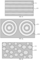
- the plurality of n-type semiconductor regions 111 may be in a shape of circular as shown in FIG. 4 a , or may be separate rectangle as shown in FIG. 4 b , or may be tangent rectangle as shown in FIG. 4 c
- the shape of the n-type semiconductor regions 111 may also be triangular as shown in FIG. 4 d ; further, the shape of the n-type semiconductor regions 111 may be a vertical strip shaped structure as shown in FIG. 4 e , or it may also be a horizontal strip shaped structure as shown in FIG.
- the concentric circle structure may be single or the same; and the shape of the n-type semiconductor regions 111 viewed from above is not specifically limited by the present application.
- a distribution of top-view shapes of the n-type semiconductor regions 111 is uniform on a surface of the high-resistance silicon substrate 110 .
- the distribution of the top-view shapes of the n-type semiconductor regions 111 may also be uneven on the surface of the high-resistance silicon substrate 110 as shown in FIG. 4 h.
- a cross-sectional shape, a top-view shape, a distribution rule, an interval size and so on of the n-type semiconductor regions 111 may be changed, as long as it can be ensured that the p-type semiconductor regions are completely depleted to form a space charge region in a lateral PN junction constituted by the n-type semiconductor regions and the p-type semiconductor regions formed by atoms diffusion, and thereby diffusion influence of Ga, Al and other atoms after growing epitaxially a compound layer is eliminated.
- the ions implanted are Phosphorus (P) ions.
- the ions implanted may also be Nitrogen (N), Arsenic (As) and other ions.
- a depth H of an ion implantation concentrations of each of the plurality of n-type semiconductor regions is 0.01 ⁇ m ⁇ 10 ⁇ m
- a maximum width W of each of the plurality of n-type semiconductor regions in a lateral direction is 0.1 ⁇ m ⁇ 2000 ⁇ m
- an interval between adjacent two of the plurality of n-type semiconductor regions is less than 2000 ⁇ m.
- a range of the ion implantation concentrations is 1E14 cm ⁇ 3 ⁇ 1E20 cm ⁇ 3
- a preferred range of the ion implantation concentration is 1E15 cm ⁇ 3 ⁇ 1E17 cm ⁇ 3 .
- the upper part of the high-resistance silicon substrate is formed into a plurality of the local n-type semiconductor regions.
- the upper part of the high-resistance silicon substrate is formed into a plurality of the local n-type semiconductor regions by a way of selective region epitaxy, specifically as follows.
- a high-resistance silicon substrate 210 is provided.
- a part of the high-resistance silicon substrate 210 requiring selective region epitaxy growth is removed, such that a plurality of trenches 211 are formed in an upper part of the high-resistance silicon substrate 210 .
- n-type semiconductor regions 212 are epitaxy grown in the trenches 211 , a doping ion concentration of the plurality of n-type semiconductor regions is 1E14 cm ⁇ 3 ⁇ 1E20 cm ⁇ 3 , and preferably, a range of concentrations is 1E15 cm ⁇ 3 ⁇ 1E17 cm ⁇ 3 .
- a depth h of each of the trenches 211 is 0.01 ⁇ m ⁇ 10 ⁇ m, a maximum width w in a lateral direction is 0.1 ⁇ m ⁇ 2000 ⁇ m, and an interval d between two adjacent trenches is less than 2000 ⁇ m.
- a shape of the n-type semiconductor regions 212 formed in the trenches 211 is the same as a cross-sectional shape, a top-view shape, a distribution rule, an interval size and so on of ion implantation regions 111 in an ion implantation method, which is not specifically limited, as long as it can be ensured that p-type semiconductor regions are completely depleted to form a space charge region in a lateral PN junction constituted by the n-type semiconductor regions of the upper part of the high-resistance silicon substrate and the p-type semiconductor regions formed by atoms diffusion, such that a diffusion influence of Ga, Al and other atoms after growing epitaxially a compound layer is eliminated.
- the upper part of the high-resistance silicon substrate may also be formed into a plurality of local n-type semiconductor regions by a way of n-type ion diffusion, specifically as follows.
- a high-resistance silicon substrate 310 is provided.
- n-type ion regions 320 are selectively epitaxy grown on an upper part of the high-resistance silicon substrate 310 , and the n-type ion includes Phosphorus (P), Nitrogen (N), Arsenic (As) and the like.
- a height a of each of the plurality of n-type ion regions is 0.01 ⁇ m ⁇ 10 ⁇ m, and a maximum width b in a lateral direction is 0.1 ⁇ m ⁇ 2000 ⁇ m, an interval c between two adjacent n-type ion regions is less than 2000 ⁇ m, such that a plurality of local n-type semiconductor regions 311 are formed in the high-resistance silicon substrate 310 as shown in FIG. 6 c .
- a doping ion concentration of the plurality of n-type semiconductor regions is 1E14 cm ⁇ 3 to 1E20 cm ⁇ 3 , and a preferred range of concentrations is 1E15 cm ⁇ 3 to 1E17 cm ⁇ 3 .
- a shape of the n-type semiconductor regions 311 formed by n-type ion diffusion is the same as a cross-sectional shape, a top-view shape, a distribution rule, an interval size and so on of ion implantation regions 111 in an ion implantation method, which is not specifically limited, as long as it can be ensured that p-type semiconductor regions are completely depleted to form a space charge region in a lateral PN junction constituted by the n-type semiconductor regions on the upper part of the high-resistance silicon substrate and the p-type semiconductor regions formed by atoms diffusion, and thereby diffusion influence of Ga, Al and other atoms after growing epitaxially a compound layer is eliminated.
- a compound layer 420 is epitaxy grown on a high-resistance silicon substrate 410 , and the compound layer 420 at least includes an element, which diffuses into the high-resistance silicon substrate and forms a p-type semiconductor region in the high-resistance silicon substrate.
- the compound layer 420 may be a III-V group compound layer containing III group atoms such as Ga, Al and the like, such as GaN, AlGaN, and AlInGaN and other semiconductor materials, and Ga and Al can diffuse into the high-resistance silicon substrate and form p-type semiconductor regions in the high-resistance silicon substrate.
- the compound layer 420 may also be a compound layer containing II group elements, elements contained in the compound layer is not limited specifically as long as it can be ensured that there is an element in the compound layer can diffuse into the high-resistance silicon substrate and form the p-type semiconductor regions in the high-resistance silicon substrate.
- atoms such as Ga, Al and the like in a compound layer 520 can diffuse into a high-resistance silicon substrate 510 after the compound layer 520 is epitaxy grown on the high-resistance silicon substrate 510 , thereby a part of the high-resistance silicon substrate 510 is transformed into a p-type semiconductor region 512 .
- the p-type semiconductor region 512 having a thickness of the p-type semiconductor region 512 ranges from 0.05 ⁇ m to 5 ⁇ m, is a conductive layer, which can seriously influence efficiency of a microwave device.
- an upper part of a high-resistance silicon substrate is formed into a plurality of n-type semiconductor regions locally arranged, and a doping concentration of the n-type semiconductor regions is greater than or equal to a doping concentration of the p-type semiconductor regions, such that, as shown in FIG. 8 b , the p-type semiconductor regions are completely depleted to form space charge region 513 in a lateral PN junction formed by the p-type semiconductor regions and the n-type semiconductor regions, and thereby diffusion influence of Ga, Al and other atoms after growing epitaxially a compound layer is eliminated.
- the semiconductor structure includes a high-resistance silicon substrate 510 including a space charge region 513 and a compound layer 520 located on the high-resistance silicon substrate 510 .
- the space charge region 513 is located in an upper part of the high-resistance silicon substrate 510 in contact with the compound layer 520 .
- the compound layer 520 at least includes an element, the element such as Ga, Al and the like diffuses into the high-resistance silicon substrate and forms a p-type semiconductor region in the high-resistance silicon substrate.
- a thickness of the space charge region is 0.01 ⁇ m ⁇ 10 ⁇ m.
- the high-resistance silicon substrate 510 also includes a plurality of n-type semiconductor regions 511 locally arranged.
- Formation methods of the plurality of local n-type semiconductor regions include n-type ion implantation, selective region epitaxy, n-type ion diffusion and the like, and donor ions in n-type semiconductor are Phosphorus (P), Nitrogen (N), and Arsenic (As) and the like.
- a depth of each of the plurality of n-type semiconductor regions is 0.01 ⁇ m ⁇ 10 ⁇ , a width in a lateral direction is 0.1 ⁇ m ⁇ 2000 ⁇ m, an interval between two adjacent n-type semiconductor regions is less than 2000 ⁇ m, a range of doping concentrations of the plurality of n-type semiconductor regions is 1E14 cm ⁇ 3 ⁇ 1E20 cm ⁇ 3 , and a preferred range of concentrations is 1E15 cm ⁇ 3 ⁇ 1E17 cm ⁇ 3 .
- a resistivity of the high-resistance silicon substrate is greater than 100 ⁇ cm.
- the resistivity of the high-resistance silicon substrate is greater than 1000 ⁇ cm.
- a thickness of the high-resistance silicon substrate is 100 ⁇ m ⁇ 1500 ⁇ m.
- the semiconductor device includes a semiconductor device (diodes, transistors, integrated circuits and the like) performing predetermined electronic functions in a controlled manner, and includes a semiconductor device (LEDs, lasers and the like) performing predetermined photonic functions in a controlled manner.
- a transistor is configured as an example to describe the semiconductor structure in detail, but the semiconductor device applied the semiconductor structure in the present application is not limited to the example in the present application.
- FIG. 9 shows a device structure of a transistor applied the semiconductor structure.
- a transistor device includes a high-resistance silicon substrate 610 , space charge region 613 , a III-V group compound layer 620 , a passivation layer 630 , a source electrode 640 , a drain electrode 650 and a gate electrode 660 .
- the III-V group compound layer 620 includes a back barrier layer 621 , a channel layer 622 , and an upper barrier layer 623 , the back barrier layer 621 and the upper barrier layer 623 may be AlGaN, and the channel layer 622 may be GaN. Further, the III-V group compound layer 620 also includes a nucleation layer 624 and a buffer layer 625 , the nucleation layer 624 may be AN, and the buffer layer 625 may be AlGaN. In other embodiments, the upper barrier layer 623 may not be disposed, and the channel layer 622 is undoped or n-doped.
- the passivation layer 630 may include silicon nitride, silicon dioxide, aluminum nitride, aluminum oxide, aluminum oxynitride and the like.
- each of the source electrode 640 and the drain electrode 650 forms an ohmic contact with the upper barrier layer 623
- the gate electrode 660 forms a schottky contact with the passivation layer 630 .
- Al and Ga atoms in the III-V group compound layer 620 diffuse into the high-resistance silicon substrate 610 , so that p-type semiconductor regions 612 are formed in a surface of the high-resistance silicon substrate.
- n-type ions such as phosphorus, nitrogen, arsenic and the like in the high-resistance silicon substrate, so that an upper part of the high-resistance silicon substrate is formed into a n-type semiconductor regions 611 in advance, and so that the p-type semiconductor regions 612 and the n-type semiconductor regions form a space charge region 613 , thereby p-type semiconductor conductive regions formed on the high-resistance silicon substrate due to diffusion of Al and Ga atoms are eliminated, a parasitic capacitance caused by a conductive substrate is greatly reduced, and a resistivity of the high-resistance silicon substrate under high temperature conditions can be improved.
- n-type ions such as phosphorus, nitrogen, arsenic and the like
- a depth of the n-type semiconductor regions 611 is greater than a thickness of the p-type semiconductor regions 612 . It can be understood that the depth of the n-type semiconductor regions 611 may be less than or equal to the thickness of the p-type semiconductor region 612 in other embodiments as long as it can be ensured that the p-type semiconductor regions are completely depleted to form the space charge region 613 or partly depleted to form unconnected space charge region 613 in a lateral PN junction constituted by the n-type semiconductor regions on an upper part of the high-resistance silicon substrate and the p-type semiconductor regions formed by atoms diffusion, and thereby diffusion influence of Ga, Al atoms after growing epitaxially the III-V group compound layer is eliminated.
- a semiconductor structure in embodiments of the present application is by performing a way such as local n-type ion implantation, selective region epitaxy growth, local n-type ion diffusion and the like to a high-resistance silicon substrate, an upper part of the high-resistance silicon substrate is formed into a plurality of local n-type semiconductor regions so as to eliminate p-type semiconductor conductive regions formed that Al, Ga atoms in a compound layer are diffused on the upper part of the high-resistance silicon substrate in a subsequent process, the entire surface of the high-resistance silicon substrate generally has high-resistance characteristics, and there are only n-type semiconductor regions locally arranged, thereby parasitic capacitance caused by a conductive substrate is greatly reduced, and resistivity of the high-resistance silicon substrate may be improved under high temperature conditions, and then efficiencies and radio frequency characteristics of a microwave device constituted by the entire semiconductor structure are improved.
- N, P, As and other atoms in the III-V group compound layer will make a part of the high-resistance silicon substrate transforms into the n-type semiconductor regions due to diffusion, which influences performance of a device, for example, an InP layer is epitaxy grown on the high-resistance silicon substrate, P atoms will diffuse into the high-resistance silicon substrate, so that a part of the high-resistance silicon substrate is transformed into the n-type semiconductor regions.
- Gallium (Ga), Boron (B), Aluminum (Al) and other ions may be pre-implanted in the high-resistance silicon substrate to make the high-resistance silicon substrate form the p-type semiconductor regions in advance, so that the lateral PN junction is constituted by the n-type semiconductor regions formed by diffusion atoms and the p-type semiconductor regions, and n-type regions are completely depleted to form the space charge region, thereby diffusion influence of N, P, and As atoms after growing epitaxially the III-V compound layer is eliminated.
- orientation or positional relationship indicated by terms “center”, “upper”, “lower”, “left”, “right”, “vertical”, “horizontal”, “inner”, “outer” and so on is based on orientation or positional relationship shown in the drawings, or orientation or positional relationship conventionally placed when an invented product is used. It is only for being convenient for describing the present application and simplifying the description, rather than indicating or implying that referred equipment or components must have a specific orientation and be constructed and operated in the specific orientation, and therefore it may not be understood as a limitation of the present application.
- terms “first”, “second”, “third” and so on are only configured to distinguish the description and may not be understood as indicating or implying relative importance.
Landscapes
- Semiconductor Integrated Circuits (AREA)
- Junction Field-Effect Transistors (AREA)
- Insulated Gate Type Field-Effect Transistor (AREA)
Abstract
Description
Claims (19)
Applications Claiming Priority (1)
| Application Number | Priority Date | Filing Date | Title |
|---|---|---|---|
| PCT/CN2018/112657 WO2020087271A1 (en) | 2018-10-30 | 2018-10-30 | Semiconductor structure and manufacturing method therefor |
Related Parent Applications (1)
| Application Number | Title | Priority Date | Filing Date |
|---|---|---|---|
| PCT/CN2018/112657 Continuation WO2020087271A1 (en) | 2018-10-30 | 2018-10-30 | Semiconductor structure and manufacturing method therefor |
Publications (2)
| Publication Number | Publication Date |
|---|---|
| US20200395441A1 US20200395441A1 (en) | 2020-12-17 |
| US11646345B2 true US11646345B2 (en) | 2023-05-09 |
Family
ID=70463404
Family Applications (1)
| Application Number | Title | Priority Date | Filing Date |
|---|---|---|---|
| US17/004,231 Active US11646345B2 (en) | 2018-10-30 | 2020-08-27 | Semiconductor structure and manufacturing method thereof |
Country Status (4)
| Country | Link |
|---|---|
| US (1) | US11646345B2 (en) |
| CN (1) | CN112889153B (en) |
| TW (1) | TWI764056B (en) |
| WO (1) | WO2020087271A1 (en) |
Families Citing this family (2)
| Publication number | Priority date | Publication date | Assignee | Title |
|---|---|---|---|---|
| CN112736128A (en) * | 2020-12-31 | 2021-04-30 | 晶能光电(江西)有限公司 | GaN-based HEMT epitaxial structure and preparation method thereof |
| CN113571572B (en) * | 2021-09-23 | 2022-05-31 | 深圳市时代速信科技有限公司 | Semiconductor device |
Citations (11)
| Publication number | Priority date | Publication date | Assignee | Title |
|---|---|---|---|---|
| CN1371133A (en) | 2002-02-26 | 2002-09-25 | 南京大学 | High-responsivity photoelectronic detector based on the polarization effect of III family nitride heterojunction structure |
| US20060003514A1 (en) | 2004-06-29 | 2006-01-05 | International Rectifier Corporation | Method of forming ohmic contact to a semiconductor body |
| US20060035449A1 (en) | 2004-08-10 | 2006-02-16 | Yoo Woo S | Method of forming ultra shallow junctions |
| US20130099249A1 (en) | 2011-10-24 | 2013-04-25 | Rosestreet Labs, Llc | Nitride uv light sensors on silicon substrates |
| US20140197462A1 (en) * | 2013-01-14 | 2014-07-17 | International Rectifier Corporation | III-Nitride Transistor with High Resistivity Substrate |
| CN104064635A (en) | 2014-05-04 | 2014-09-24 | 易美芯光(北京)科技有限公司 | A kind of preparation method of LED chip with vertical structure |
| WO2015054982A1 (en) | 2013-10-15 | 2015-04-23 | 苏州晶湛半导体有限公司 | Nitride power transistor and manufacturing method thereof |
| US20150318360A1 (en) * | 2012-12-11 | 2015-11-05 | Massachusetts Institute Of Technology | Reducing leakage current in semiconductor devices |
| CN205376554U (en) | 2015-12-01 | 2016-07-06 | 傲迪特半导体(南京)有限公司 | Silicon photodiode |
| TW201837991A (en) | 2017-03-31 | 2018-10-16 | 環球晶圓股份有限公司 | Epitaxial substrate and method of manufacturing same |
| US20200075314A1 (en) * | 2018-08-29 | 2020-03-05 | Taiwan Semiconductor Manufacturing Co., Ltd. | Doped buffer layer for group iii-v devices on silicon |
Family Cites Families (7)
| Publication number | Priority date | Publication date | Assignee | Title |
|---|---|---|---|---|
| US5559359A (en) * | 1994-07-29 | 1996-09-24 | Reyes; Adolfo C. | Microwave integrated circuit passive element structure and method for reducing signal propagation losses |
| JP2002314098A (en) * | 2001-04-13 | 2002-10-25 | Sanken Electric Co Ltd | Semiconductor device |
| JP2013048212A (en) * | 2011-07-28 | 2013-03-07 | Sony Corp | Semiconductor device and semiconductor device manufacturing method |
| CN102446956B (en) * | 2011-09-05 | 2016-02-17 | 万小敏 | Semiconductor high-power device and manufacturing method thereof |
| NL2011568A (en) * | 2012-10-31 | 2014-05-06 | Asml Netherlands Bv | Sensor and lithographic apparatus. |
| US9806182B2 (en) * | 2015-09-08 | 2017-10-31 | Macom Technology Solutions Holdings, Inc. | Parasitic channel mitigation using elemental diboride diffusion barrier regions |
| US10644142B2 (en) * | 2017-12-22 | 2020-05-05 | Nxp Usa, Inc. | Semiconductor devices with doped regions functioning as enhanced resistivity regions or diffusion barriers, and methods of fabrication therefor |
-
2018
- 2018-10-30 CN CN201880096940.1A patent/CN112889153B/en active Active
- 2018-10-30 WO PCT/CN2018/112657 patent/WO2020087271A1/en not_active Ceased
-
2019
- 2019-10-18 TW TW108137650A patent/TWI764056B/en active
-
2020
- 2020-08-27 US US17/004,231 patent/US11646345B2/en active Active
Patent Citations (12)
| Publication number | Priority date | Publication date | Assignee | Title |
|---|---|---|---|---|
| CN1371133A (en) | 2002-02-26 | 2002-09-25 | 南京大学 | High-responsivity photoelectronic detector based on the polarization effect of III family nitride heterojunction structure |
| US20060003514A1 (en) | 2004-06-29 | 2006-01-05 | International Rectifier Corporation | Method of forming ohmic contact to a semiconductor body |
| US20060035449A1 (en) | 2004-08-10 | 2006-02-16 | Yoo Woo S | Method of forming ultra shallow junctions |
| US20130099249A1 (en) | 2011-10-24 | 2013-04-25 | Rosestreet Labs, Llc | Nitride uv light sensors on silicon substrates |
| US20150318360A1 (en) * | 2012-12-11 | 2015-11-05 | Massachusetts Institute Of Technology | Reducing leakage current in semiconductor devices |
| US20140197462A1 (en) * | 2013-01-14 | 2014-07-17 | International Rectifier Corporation | III-Nitride Transistor with High Resistivity Substrate |
| WO2015054982A1 (en) | 2013-10-15 | 2015-04-23 | 苏州晶湛半导体有限公司 | Nitride power transistor and manufacturing method thereof |
| US20160233329A1 (en) * | 2013-10-15 | 2016-08-11 | Enkris Semiconductor, Inc. | Nitride power transistor and manufacturing method thereof |
| CN104064635A (en) | 2014-05-04 | 2014-09-24 | 易美芯光(北京)科技有限公司 | A kind of preparation method of LED chip with vertical structure |
| CN205376554U (en) | 2015-12-01 | 2016-07-06 | 傲迪特半导体(南京)有限公司 | Silicon photodiode |
| TW201837991A (en) | 2017-03-31 | 2018-10-16 | 環球晶圓股份有限公司 | Epitaxial substrate and method of manufacturing same |
| US20200075314A1 (en) * | 2018-08-29 | 2020-03-05 | Taiwan Semiconductor Manufacturing Co., Ltd. | Doped buffer layer for group iii-v devices on silicon |
Non-Patent Citations (2)
| Title |
|---|
| International Search Report issued in corresponding PCT Application No. PCT/CN2018/112657, dated Jun. 20, 2019. |
| Written Opinion issued in corresponding PCT Application No. PCT/CN2018/112657, dated Jun. 20, 2019. |
Also Published As
| Publication number | Publication date |
|---|---|
| CN112889153A (en) | 2021-06-01 |
| WO2020087271A1 (en) | 2020-05-07 |
| TWI764056B (en) | 2022-05-11 |
| CN112889153B (en) | 2024-04-26 |
| US20200395441A1 (en) | 2020-12-17 |
| TW202025249A (en) | 2020-07-01 |
Similar Documents
| Publication | Publication Date | Title |
|---|---|---|
| US8343823B2 (en) | Nanowire and larger GaN based HEMTs | |
| US10243066B2 (en) | Producing a semiconductor device by epitaxial growth | |
| US9012311B2 (en) | Method for producing a semiconductor body having a recombination zone, semiconductor component having a recombination zone, and method for producing such a semiconductor component | |
| US8138581B2 (en) | Semiconductor device with channel stop trench and method | |
| US10546944B2 (en) | Semiconductor device and method of fabricating the same | |
| US8956960B2 (en) | Method for stress reduced manufacturing semiconductor devices | |
| US11646345B2 (en) | Semiconductor structure and manufacturing method thereof | |
| US8823140B2 (en) | GaN vertical bipolar transistor | |
| DE102014114897A1 (en) | A method of fabricating a vertical semiconductor device and a vertical semiconductor device | |
| US11289595B2 (en) | Power semiconductor device and method | |
| US8803230B2 (en) | Semiconductor transistor having trench contacts and method for forming therefor | |
| US10665705B2 (en) | Semiconductor device with deep diffusion region | |
| US11018252B2 (en) | Power semiconductor transistor | |
| US9524960B2 (en) | Vertical transistor with flashover protection | |
| US10446642B2 (en) | Epitaxial substrate and method for forming the same | |
| US7692268B2 (en) | Integrated circuit with bipolar transistor | |
| CN103943670A (en) | Super-junction collector region strained silicon heterojunction bipolar transistor | |
| US20240072109A1 (en) | Device for high voltage applications | |
| US7466004B2 (en) | Diode structure to suppress parasitic current | |
| CN121335427A (en) | A method for manufacturing a semiconductor structure | |
| EP1575094A1 (en) | Bipolar transistor | |
| CN114503020A (en) | Electro-optic modulator |
Legal Events
| Date | Code | Title | Description |
|---|---|---|---|
| AS | Assignment |
Owner name: ENKRIS SEMICONDUCTOR, INC., CHINA Free format text: ASSIGNMENT OF ASSIGNORS INTEREST;ASSIGNOR:CHENG, KAI;REEL/FRAME:053612/0534 Effective date: 20200618 |
|
| FEPP | Fee payment procedure |
Free format text: ENTITY STATUS SET TO UNDISCOUNTED (ORIGINAL EVENT CODE: BIG.); ENTITY STATUS OF PATENT OWNER: SMALL ENTITY |
|
| FEPP | Fee payment procedure |
Free format text: ENTITY STATUS SET TO SMALL (ORIGINAL EVENT CODE: SMAL); ENTITY STATUS OF PATENT OWNER: SMALL ENTITY |
|
| STPP | Information on status: patent application and granting procedure in general |
Free format text: APPLICATION DISPATCHED FROM PREEXAM, NOT YET DOCKETED |
|
| STPP | Information on status: patent application and granting procedure in general |
Free format text: DOCKETED NEW CASE - READY FOR EXAMINATION |
|
| STPP | Information on status: patent application and granting procedure in general |
Free format text: NON FINAL ACTION MAILED |
|
| STPP | Information on status: patent application and granting procedure in general |
Free format text: RESPONSE TO NON-FINAL OFFICE ACTION ENTERED AND FORWARDED TO EXAMINER |
|
| STPP | Information on status: patent application and granting procedure in general |
Free format text: FINAL REJECTION MAILED |
|
| STPP | Information on status: patent application and granting procedure in general |
Free format text: DOCKETED NEW CASE - READY FOR EXAMINATION |
|
| STPP | Information on status: patent application and granting procedure in general |
Free format text: NON FINAL ACTION MAILED |
|
| STPP | Information on status: patent application and granting procedure in general |
Free format text: RESPONSE TO NON-FINAL OFFICE ACTION ENTERED AND FORWARDED TO EXAMINER |
|
| STCF | Information on status: patent grant |
Free format text: PATENTED CASE |