US11588061B2 - Photoelectric conversion module and method for manufacturing photoelectric conversion module - Google Patents
Photoelectric conversion module and method for manufacturing photoelectric conversion module Download PDFInfo
- Publication number
- US11588061B2 US11588061B2 US16/646,948 US201816646948A US11588061B2 US 11588061 B2 US11588061 B2 US 11588061B2 US 201816646948 A US201816646948 A US 201816646948A US 11588061 B2 US11588061 B2 US 11588061B2
- Authority
- US
- United States
- Prior art keywords
- photoelectric conversion
- layer
- electrode layer
- grid
- grid electrode
- Prior art date
- Legal status (The legal status is an assumption and is not a legal conclusion. Google has not performed a legal analysis and makes no representation as to the accuracy of the status listed.)
- Active
Links
- 238000006243 chemical reaction Methods 0.000 title claims abstract description 204
- 238000004519 manufacturing process Methods 0.000 title claims description 15
- 238000000034 method Methods 0.000 title claims description 13
- 239000000758 substrate Substances 0.000 claims abstract description 26
- 238000002834 transmittance Methods 0.000 claims description 24
- 239000004065 semiconductor Substances 0.000 claims description 19
- 238000010304 firing Methods 0.000 claims description 12
- 238000010438 heat treatment Methods 0.000 claims description 7
- XLOMVQKBTHCTTD-UHFFFAOYSA-N Zinc monoxide Chemical compound [Zn]=O XLOMVQKBTHCTTD-UHFFFAOYSA-N 0.000 claims description 5
- 229910052751 metal Inorganic materials 0.000 claims description 5
- 239000002184 metal Substances 0.000 claims description 5
- 229910021476 group 6 element Inorganic materials 0.000 claims description 3
- VYZAMTAEIAYCRO-UHFFFAOYSA-N Chromium Chemical compound [Cr] VYZAMTAEIAYCRO-UHFFFAOYSA-N 0.000 claims description 2
- ZOKXTWBITQBERF-UHFFFAOYSA-N Molybdenum Chemical compound [Mo] ZOKXTWBITQBERF-UHFFFAOYSA-N 0.000 claims description 2
- RTAQQCXQSZGOHL-UHFFFAOYSA-N Titanium Chemical compound [Ti] RTAQQCXQSZGOHL-UHFFFAOYSA-N 0.000 claims description 2
- 229910052804 chromium Inorganic materials 0.000 claims description 2
- 239000011651 chromium Substances 0.000 claims description 2
- 150000001875 compounds Chemical class 0.000 claims description 2
- AMGQUBHHOARCQH-UHFFFAOYSA-N indium;oxotin Chemical compound [In].[Sn]=O AMGQUBHHOARCQH-UHFFFAOYSA-N 0.000 claims description 2
- 229910052750 molybdenum Inorganic materials 0.000 claims description 2
- 239000011733 molybdenum Substances 0.000 claims description 2
- 229910052719 titanium Inorganic materials 0.000 claims description 2
- 239000010936 titanium Substances 0.000 claims description 2
- 239000011787 zinc oxide Substances 0.000 claims description 2
- 239000000463 material Substances 0.000 description 30
- 239000010408 film Substances 0.000 description 26
- 230000004048 modification Effects 0.000 description 12
- 238000012986 modification Methods 0.000 description 12
- 239000000047 product Substances 0.000 description 9
- 238000013459 approach Methods 0.000 description 4
- 238000009826 distribution Methods 0.000 description 4
- 239000011521 glass Substances 0.000 description 4
- 239000011701 zinc Substances 0.000 description 4
- 230000008878 coupling Effects 0.000 description 3
- 238000010168 coupling process Methods 0.000 description 3
- 238000005859 coupling reaction Methods 0.000 description 3
- 239000013078 crystal Substances 0.000 description 3
- 238000005520 cutting process Methods 0.000 description 3
- 239000003574 free electron Substances 0.000 description 3
- 239000010409 thin film Substances 0.000 description 3
- 239000004020 conductor Substances 0.000 description 2
- 229910052802 copper Inorganic materials 0.000 description 2
- 239000010949 copper Substances 0.000 description 2
- 239000002270 dispersing agent Substances 0.000 description 2
- 238000007641 inkjet printing Methods 0.000 description 2
- 239000003960 organic solvent Substances 0.000 description 2
- 239000002245 particle Substances 0.000 description 2
- 230000009467 reduction Effects 0.000 description 2
- 239000011265 semifinished product Substances 0.000 description 2
- 229910052709 silver Inorganic materials 0.000 description 2
- 238000004544 sputter deposition Methods 0.000 description 2
- RYGMFSIKBFXOCR-UHFFFAOYSA-N Copper Chemical compound [Cu] RYGMFSIKBFXOCR-UHFFFAOYSA-N 0.000 description 1
- 230000005355 Hall effect Effects 0.000 description 1
- 229910003363 ZnMgO Inorganic materials 0.000 description 1
- 229910052782 aluminium Inorganic materials 0.000 description 1
- 230000008901 benefit Effects 0.000 description 1
- 239000011230 binding agent Substances 0.000 description 1
- 230000015572 biosynthetic process Effects 0.000 description 1
- 239000000919 ceramic Substances 0.000 description 1
- 230000007797 corrosion Effects 0.000 description 1
- 238000005260 corrosion Methods 0.000 description 1
- 230000006378 damage Effects 0.000 description 1
- 230000006866 deterioration Effects 0.000 description 1
- 238000001704 evaporation Methods 0.000 description 1
- 230000004907 flux Effects 0.000 description 1
- 229910052733 gallium Inorganic materials 0.000 description 1
- 229910052737 gold Inorganic materials 0.000 description 1
- 229910052738 indium Inorganic materials 0.000 description 1
- 238000007733 ion plating Methods 0.000 description 1
- 238000005259 measurement Methods 0.000 description 1
- 238000002488 metal-organic chemical vapour deposition Methods 0.000 description 1
- 239000012299 nitrogen atmosphere Substances 0.000 description 1
- 238000007645 offset printing Methods 0.000 description 1
- -1 or the like) Inorganic materials 0.000 description 1
- 229910052760 oxygen Inorganic materials 0.000 description 1
- 238000007639 printing Methods 0.000 description 1
- 239000011347 resin Substances 0.000 description 1
- 229920005989 resin Polymers 0.000 description 1
- 238000007650 screen-printing Methods 0.000 description 1
- 239000003566 sealing material Substances 0.000 description 1
- 229910052711 selenium Inorganic materials 0.000 description 1
- 239000004332 silver Substances 0.000 description 1
- 229910052717 sulfur Inorganic materials 0.000 description 1
- 229910052714 tellurium Inorganic materials 0.000 description 1
Images


Classifications
-
- H—ELECTRICITY
- H01—ELECTRIC ELEMENTS
- H01L—SEMICONDUCTOR DEVICES NOT COVERED BY CLASS H10
- H01L31/00—Semiconductor devices sensitive to infrared radiation, light, electromagnetic radiation of shorter wavelength or corpuscular radiation and specially adapted either for the conversion of the energy of such radiation into electrical energy or for the control of electrical energy by such radiation; Processes or apparatus specially adapted for the manufacture or treatment thereof or of parts thereof; Details thereof
- H01L31/04—Semiconductor devices sensitive to infrared radiation, light, electromagnetic radiation of shorter wavelength or corpuscular radiation and specially adapted either for the conversion of the energy of such radiation into electrical energy or for the control of electrical energy by such radiation; Processes or apparatus specially adapted for the manufacture or treatment thereof or of parts thereof; Details thereof adapted as photovoltaic [PV] conversion devices
- H01L31/042—PV modules or arrays of single PV cells
- H01L31/0445—PV modules or arrays of single PV cells including thin film solar cells, e.g. single thin film a-Si, CIS or CdTe solar cells
- H01L31/046—PV modules composed of a plurality of thin film solar cells deposited on the same substrate
-
- H—ELECTRICITY
- H01—ELECTRIC ELEMENTS
- H01L—SEMICONDUCTOR DEVICES NOT COVERED BY CLASS H10
- H01L31/00—Semiconductor devices sensitive to infrared radiation, light, electromagnetic radiation of shorter wavelength or corpuscular radiation and specially adapted either for the conversion of the energy of such radiation into electrical energy or for the control of electrical energy by such radiation; Processes or apparatus specially adapted for the manufacture or treatment thereof or of parts thereof; Details thereof
- H01L31/02—Details
- H01L31/0224—Electrodes
- H01L31/022408—Electrodes for devices characterised by at least one potential jump barrier or surface barrier
- H01L31/022425—Electrodes for devices characterised by at least one potential jump barrier or surface barrier for solar cells
- H01L31/022433—Particular geometry of the grid contacts
-
- H—ELECTRICITY
- H01—ELECTRIC ELEMENTS
- H01L—SEMICONDUCTOR DEVICES NOT COVERED BY CLASS H10
- H01L31/00—Semiconductor devices sensitive to infrared radiation, light, electromagnetic radiation of shorter wavelength or corpuscular radiation and specially adapted either for the conversion of the energy of such radiation into electrical energy or for the control of electrical energy by such radiation; Processes or apparatus specially adapted for the manufacture or treatment thereof or of parts thereof; Details thereof
- H01L31/02—Details
- H01L31/0224—Electrodes
- H01L31/022466—Electrodes made of transparent conductive layers, e.g. TCO, ITO layers
-
- H—ELECTRICITY
- H01—ELECTRIC ELEMENTS
- H01L—SEMICONDUCTOR DEVICES NOT COVERED BY CLASS H10
- H01L31/00—Semiconductor devices sensitive to infrared radiation, light, electromagnetic radiation of shorter wavelength or corpuscular radiation and specially adapted either for the conversion of the energy of such radiation into electrical energy or for the control of electrical energy by such radiation; Processes or apparatus specially adapted for the manufacture or treatment thereof or of parts thereof; Details thereof
- H01L31/0248—Semiconductor devices sensitive to infrared radiation, light, electromagnetic radiation of shorter wavelength or corpuscular radiation and specially adapted either for the conversion of the energy of such radiation into electrical energy or for the control of electrical energy by such radiation; Processes or apparatus specially adapted for the manufacture or treatment thereof or of parts thereof; Details thereof characterised by their semiconductor bodies
- H01L31/0352—Semiconductor devices sensitive to infrared radiation, light, electromagnetic radiation of shorter wavelength or corpuscular radiation and specially adapted either for the conversion of the energy of such radiation into electrical energy or for the control of electrical energy by such radiation; Processes or apparatus specially adapted for the manufacture or treatment thereof or of parts thereof; Details thereof characterised by their semiconductor bodies characterised by their shape or by the shapes, relative sizes or disposition of the semiconductor regions
- H01L31/035272—Semiconductor devices sensitive to infrared radiation, light, electromagnetic radiation of shorter wavelength or corpuscular radiation and specially adapted either for the conversion of the energy of such radiation into electrical energy or for the control of electrical energy by such radiation; Processes or apparatus specially adapted for the manufacture or treatment thereof or of parts thereof; Details thereof characterised by their semiconductor bodies characterised by their shape or by the shapes, relative sizes or disposition of the semiconductor regions characterised by at least one potential jump barrier or surface barrier
-
- H—ELECTRICITY
- H01—ELECTRIC ELEMENTS
- H01L—SEMICONDUCTOR DEVICES NOT COVERED BY CLASS H10
- H01L31/00—Semiconductor devices sensitive to infrared radiation, light, electromagnetic radiation of shorter wavelength or corpuscular radiation and specially adapted either for the conversion of the energy of such radiation into electrical energy or for the control of electrical energy by such radiation; Processes or apparatus specially adapted for the manufacture or treatment thereof or of parts thereof; Details thereof
- H01L31/18—Processes or apparatus specially adapted for the manufacture or treatment of these devices or of parts thereof
- H01L31/1884—Manufacture of transparent electrodes, e.g. TCO, ITO
-
- Y—GENERAL TAGGING OF NEW TECHNOLOGICAL DEVELOPMENTS; GENERAL TAGGING OF CROSS-SECTIONAL TECHNOLOGIES SPANNING OVER SEVERAL SECTIONS OF THE IPC; TECHNICAL SUBJECTS COVERED BY FORMER USPC CROSS-REFERENCE ART COLLECTIONS [XRACs] AND DIGESTS
- Y02—TECHNOLOGIES OR APPLICATIONS FOR MITIGATION OR ADAPTATION AGAINST CLIMATE CHANGE
- Y02E—REDUCTION OF GREENHOUSE GAS [GHG] EMISSIONS, RELATED TO ENERGY GENERATION, TRANSMISSION OR DISTRIBUTION
- Y02E10/00—Energy generation through renewable energy sources
- Y02E10/50—Photovoltaic [PV] energy
- Y02E10/541—CuInSe2 material PV cells
-
- Y—GENERAL TAGGING OF NEW TECHNOLOGICAL DEVELOPMENTS; GENERAL TAGGING OF CROSS-SECTIONAL TECHNOLOGIES SPANNING OVER SEVERAL SECTIONS OF THE IPC; TECHNICAL SUBJECTS COVERED BY FORMER USPC CROSS-REFERENCE ART COLLECTIONS [XRACs] AND DIGESTS
- Y02—TECHNOLOGIES OR APPLICATIONS FOR MITIGATION OR ADAPTATION AGAINST CLIMATE CHANGE
- Y02E—REDUCTION OF GREENHOUSE GAS [GHG] EMISSIONS, RELATED TO ENERGY GENERATION, TRANSMISSION OR DISTRIBUTION
- Y02E10/00—Energy generation through renewable energy sources
- Y02E10/50—Photovoltaic [PV] energy
- Y02E10/548—Amorphous silicon PV cells
-
- Y—GENERAL TAGGING OF NEW TECHNOLOGICAL DEVELOPMENTS; GENERAL TAGGING OF CROSS-SECTIONAL TECHNOLOGIES SPANNING OVER SEVERAL SECTIONS OF THE IPC; TECHNICAL SUBJECTS COVERED BY FORMER USPC CROSS-REFERENCE ART COLLECTIONS [XRACs] AND DIGESTS
- Y02—TECHNOLOGIES OR APPLICATIONS FOR MITIGATION OR ADAPTATION AGAINST CLIMATE CHANGE
- Y02P—CLIMATE CHANGE MITIGATION TECHNOLOGIES IN THE PRODUCTION OR PROCESSING OF GOODS
- Y02P70/00—Climate change mitigation technologies in the production process for final industrial or consumer products
- Y02P70/50—Manufacturing or production processes characterised by the final manufactured product
Definitions
- the present invention relates to a photoelectric conversion module having a grid electrode and a method for manufacturing the photoelectric conversion module.
- a photoelectric conversion module such as a solar battery module including a plurality of photoelectric conversion cells is known (following Patent Literature 1).
- a photoelectric conversion cell includes a transparent electrode layer located on a light receiving surface, a rear surface electrode layer located on a surface opposite to the light receiving surface, and a photoelectric conversion layer between the transparent electrode layer and the rear surface electrode layer.
- An electric resistance value of the transparent electrode layer is generally higher than an electric resistance value of an opaque electrode layer made of metal. Therefore, when a current generated by the photoelectric conversion flows through the transparent electrode layer, a power loss occurs due to the electric resistance value of the transparent electrode layer.
- a grid electrode (collecting electrode) made of a thin line metal is provided on the transparent electrode layer in some cases.
- the path of the current flowing through the transparent electrode layer is shortened by collecting the current flowing through the transparent electrode layer into the grid electrode. Therefore, power loss due to the electric resistance value of the transparent electrode layer can be reduced.
- connection failure may occur between the grid electrode and the transparent electrode layer, or flux at the time of forming the grid electrode may remain as a residue under the grid electrode, which increases the contact resistance between the grid electrode and the transparent electrode layer in some cases. In this case, the current collecting ability of the grid electrode is reduced, which may cause a decrease in the conversion efficiency of the photoelectric conversion module.
- a photoelectric conversion module comprises: a photoelectric conversion cell including a first electrode layer, a second electrode layer, a photoelectric conversion layer between the first electrode layer and the second electrode layer on a substrate; and a grid electrode provided in the photoelectric conversion cell, wherein the second electrode layer is formed of a transparent electrode layer located on opposite side of the photoelectric conversion layer to the substrate, and the grid electrode is provided between the photoelectric conversion layer and the transparent electrode layer.
- a method for manufacturing a photoelectric conversion module comprises: preparing a substrate on which a first electrode layer and a photoelectric conversion layer are formed; providing a conductive ink for forming a grid electrode on the photoelectric conversion layer; a firing step of firing the conductive ink to form the grid electrode; and a step of forming a second electrode layer on the conductive ink, wherein the firing step is performed by a heat treatment during the step of forming the second electrode layer.
- FIG. 1 is a schematic top view of a photoelectric conversion module according to a first embodiment.
- FIG. 2 is a schematic top view of the photoelectric conversion module in a region 2 R in FIG. 1 .
- FIG. 3 is a schematic cross-sectional view of the photoelectric conversion module taken along line 3 A- 3 A in FIG. 2 .
- FIG. 4 is a schematic perspective view of the photoelectric conversion module in a region 4 R in FIG. 2 .
- FIG. 5 is a schematic cross-sectional view of the photoelectric conversion module taken along line 5 A- 5 A in FIG. 1 .
- FIG. 6 is a schematic top view of the photoelectric conversion module in a region 6 R in FIG. 1 .
- FIG. 7 is a schematic top view of the photoelectric conversion module in a region 7 R in FIG. 1 .
- FIG. 8 is a schematic cross-sectional view of a photoelectric conversion module according to a second embodiment.
- FIG. 9 is a schematic cross-sectional view of a photoelectric conversion module according to a third embodiment.
- FIG. 10 is a schematic top view of a connection portion between a first grid electrode and a second grid electrode according to a first modification.
- FIG. 11 is a schematic top view of a connection portion between a first grid electrode and a second grid electrode according to a second modification.
- FIG. 12 is a schematic top view of a connection portion between a first grid electrode and a second grid electrode according to a third modification.
- FIG. 13 is a schematic cross-sectional view illustrating a cell forming step in a method for manufacturing a photoelectric conversion module.
- FIG. 14 is a schematic view illustrating a first grid forming step of forming a first grid electrode.
- FIG. 15 is a schematic view illustrating a second grid forming step of forming a second grid electrode.
- FIG. 16 is a schematic view illustrating one step of a step of forming a wire.
- FIG. 17 is a schematic view illustrating steps subsequent to FIG. 16 .
- FIG. 18 is a schematic view illustrating a step of cutting out a part of the photoelectric conversion module.
- FIG. 1 is a schematic top view of a photoelectric conversion module according to a first embodiment.
- FIG. 2 is a schematic top view of the photoelectric conversion module in a region 2 R in FIG. 1 .
- FIG. 3 is a schematic cross-sectional view of the photoelectric conversion module taken along line 3 A- 3 A in FIG. 2 .
- FIG. 4 is a schematic perspective view of the photoelectric conversion module in a region 4 R in FIG. 2 .
- FIG. 5 is a schematic cross-sectional view of the photoelectric conversion module taken along line 5 A- 5 A in FIG. 1
- FIG. 6 is a schematic top view of the photoelectric conversion module in a region 6 R in FIG. 1 .
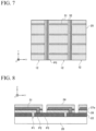
- FIG. 7 is a schematic top view of the photoelectric conversion module in a region 7 R in FIG. 1 .
- FIGS. 2 , 6 and 7 a lower layer than a second electrode layer 24 described later is drawn in perspective for convenience. Moreover, FIG. 4 does not illustrate a second electrode layer 24 described later in order to show a structure of a photoelectric conversion cell clearly for convenience.
- a photoelectric conversion module 10 may be an integrated thin-film photoelectric conversion module including a plurality of photoelectric conversion cells 12 integrated on a substrate 20 .
- the photoelectric conversion module 10 is a solar cell module that converts light energy into electric energy.
- the substrate 20 may be made of, for example, glass, ceramics, resin, metal, or the like.
- the photoelectric conversion cell 12 may have a substantially band shape when viewed from a direction orthogonal to a main surface of the substrate 20 .
- Each of the photoelectric conversion cells 12 may extend long in a first direction (the Y direction in the drawing).
- the plurality of photoelectric conversion cells 12 are arranged side by side in a second direction (the X direction in the drawing) intersecting the first direction.
- the photoelectric conversion cells 12 adjacent to each other may be divided from each other by division parts P 1 , P 2 , P 3 extending in the first direction.
- Each of the photoelectric conversion cells 12 may include at least a first electrode layer 22 , a second electrode layer 24 and a photoelectric conversion layer 26 .
- the photoelectric conversion layer 26 is provided between the first electrode layer 22 and the second electrode layer 24 .
- the first electrode layer 22 is provided between the photoelectric conversion layer 26 and the substrate 20 .
- the second electrode layer 24 is located on opposite side of the photoelectric conversion layer 26 to the substrate 20 .
- the second electrode layer 24 may be formed of a transparent electrode layer.
- the second electrode layer 24 is formed of a transparent electrode layer, light incident on the photoelectric conversion layer 26 or emitted from the photoelectric conversion layer 26 passes through the second electrode layer 24 .
- the first electrode layer 22 may be formed of an opaque electrode layer or may be formed of a transparent electrode layer.
- the first electrode layer 22 is formed of a metal such as molybdenum, titanium or chromium, for example, from the viewpoint of corrosion resistance to Group VI elements.
- the second electrode layer 24 is formed of an n-type semiconductor, more specifically, a material having n-type conductivity, a wide bandgap, and relatively low resistance.
- the second electrode layer 24 may be made of, for example, zinc oxide (ZnO) added with a group III element or indium tin oxide (ITO).
- ZnO zinc oxide
- ITO indium tin oxide
- the second electrode layer 24 can function as both an n-type semiconductor and a transparent electrode layer.
- the photoelectric conversion layer 26 may include, for example, p-type semiconductor.
- the photoelectric conversion layer 26 is formed of a compound semiconductor including a group I element (Cu, Ag, Au, or the like), a group III element (Al, Ga, In, or the like), and a group VI element (O, S, Se, Te, or the like).
- the photoelectric conversion layer 26 is not limited to those described above, and may be made of any material that causes photoelectric conversion.
- the configuration of the photoelectric conversion cell 12 is not limited to the above-described embodiment, and can take various embodiments.
- the photoelectric conversion cell 12 may have a configuration in which both an n-type semiconductor and a p-type semiconductor are sandwiched between the first electrode layer and the second electrode layer.
- the second electrode layer may not be formed of an n-type semiconductor.
- the photoelectric conversion cell 12 is not limited to a p-n junction structure, and may have a p-i-n junction structure including an intrinsic semiconductor layer (i-type semiconductor) between an n-type semiconductor and a p-type semiconductor.
- the first electrode layers 22 of the photoelectric conversion cells 12 adjacent to each other are electrically divided from each other by the division part P 1 .
- the second electrode layers 24 of the photoelectric conversion cells 12 adjacent to each other are electrically divided from each other by the division part P 3 .
- the photoelectric conversion layers 26 of the photoelectric conversion cells 12 adjacent to each other are divided from each other by the division parts P 2 , P 3 .
- the photoelectric conversion module 10 may have an electrical connection part 34 between the photoelectric conversion cells 12 adjacent to each other.
- the electrical connection part 34 electrically connects the photoelectric conversion cells 12 adjacent to each other in series.
- the electrical connection part 34 extends in the thickness direction of the photoelectric conversion module 10 at the second division part P 2 , thereby electrically connecting the first electrode layer 22 of one photoelectric conversion cell 12 and the second electrode layer 24 of the other photoelectric conversion cell 12 to each other.
- the photoelectric conversion module 10 has a plurality of first grid electrodes 31 arrayed in the first direction (the Y direction in the drawing) in each photoelectric conversion cell 12 .
- Each first grid electrode 31 extends in the second direction (the X direction in the drawing) intersecting the first direction.
- the first grid electrode 31 may be provided between the photoelectric conversion layers 26 and the second electrode layer 24 in each photoelectric conversion cell 12 .
- the first grid electrode 31 may be made of a material having higher conductivity than that of the transparent electrode layer forming the second electrode layer 24 .
- the first grid electrode 31 may be in direct contact with the transparent electrode layer.
- the width of the first grid electrode 31 in the first direction (the Y direction in the drawing) may be, for example, 5 to 100 ⁇ m.
- the thickness of the first grid electrode 31 may be, for example, 0.1 to 20 ⁇ m.
- the second grid electrode 32 extending in the first direction may be provided at an end of the first grid electrode 31 in the second direction (the X direction in the drawing).
- the second grid electrode 32 is coupled to the first grid electrode 31 at one end of the first grid electrode 31 .
- the width of the second grid electrode 32 in the second direction (the X direction in the drawing) may be, for example, 5 to 200 ⁇ m.
- the thickness of the second grid electrode 32 may be, for example, 0.1 to 20 ⁇ m.
- the first grid electrode 31 and/or the second grid electrode 32 are provided between the photoelectric conversion layer 26 and the second electrode layer (transparent electrode layer) 24 . That is, the first grid electrode 31 and/or the second grid electrode 32 are covered with the transparent electrode layer. As a result, connection failure of the first grid electrode 31 and/or the second grid electrode 32 to the transparent electrode can be suppressed. Therefore, it is possible to suppress a decrease in the current collection ability of the first grid electrode 31 and/or the second grid electrode 32 , and as a result, it is possible to suppress a decrease in the conversion efficiency of the photoelectric conversion module.
- the first grid electrode 31 and/or the second grid electrode 32 be separated from the photoelectric conversion layer 26 in the thickness direction.
- the first grid electrode 31 and/or the second grid electrode 32 are separated from the photoelectric conversion layer 26 via the transparent electrode layer 25 in the thickness direction. That is, the first grid electrode 31 and/or the second grid electrode 32 are sandwiched between the two transparent electrode layers in the thickness direction.
- the two transparent electrode layers 24 , 25 may be made of the same material or may be made of different materials.
- connection failure of the first grid electrode 31 and/or the second grid electrode 32 to the transparent electrode can be suppressed more.
- the electrical connection part 34 is formed by a portion continuous from the transparent electrode layer 25 .
- the electrical connection part 34 may be made of the same material as that of the transparent electrode layer 25 .
- the electrical connection part 34 may be made of a conductive material different from that of the transparent electrode layer 25 .
- the electrical connection part 34 may be made of the same material as that of the first grid electrode 31 or the second grid electrode 32 .
- the thickness of the first grid electrode 31 may be gradually increased toward the intersection of the first grid electrode 31 and the second grid electrode 32 (or the electrical connection part 34 ).
- the thickness of the second grid electrode 32 (or the electrical connection part 34 ) may be gradually increased toward the intersection of the first grid electrode 31 and the second grid electrode 32 (or the electrical connection part 34 ).
- the photoelectric conversion module 10 has an electric wire 50 for supplying power to the photoelectric conversion module 10 or extracting power from the photoelectric conversion module 10 .
- the wire 50 may be provided adjacent to the photoelectric conversion cell 12 located at the end of the photoelectric conversion module 10 in the second direction (the X direction in the drawing).
- the transparent electrode layers 24 , 25 may include a region 2 R as illustrated in FIG. 2 and a region 6 R as illustrated in FIG. 6 .
- the region 2 R and the region 6 R are arranged in the same photoelectric conversion cell 12 .
- the interval between the first grid electrodes 31 adjacent to each other in the first direction (Y direction) in the region 2 R is smaller than the interval between the first grid electrodes 31 adjacent to each other in the first direction (Y direction) in the region 6 R.
- the region 6 R of the transparent electrode layers 24 , 25 have sheet resistance smaller than the sheet resistance in the region 2 R, a film thickness larger than the film thickness in the region 2 R, or transmittance smaller than the transmittance in the region 2 R.
- the above-mentioned interval between the first grid electrodes 31 is an interval between a center line of an arbitrary first grid electrode 31 and a center line of an adjacent first grid electrode 31 .
- the sheet resistance, the film thickness and the transmittance of the transparent electrode layers 24 , 25 are specified respectively by the sheet resistance, the film thickness, and the transmittance of the laminate composed of the transparent electrode layer constituting the second electrode layer 24 and the transparent electrode layer 25 .
- the sheet resistance, the film thickness, and the transmittance of the transparent electrode layers 24 , 25 described above can be read respectively as the sheet resistance, the film thickness, and the transmittance of only the transparent electrode layer constituting the second electrode layer 24 (the same applies hereinafter).
- the transparent electrode layers 24 , 25 may further include a region 7 R as illustrated in FIG. 7 .
- the region 6 R and the region 7 R are arranged in different photoelectric conversion cells 12 .
- the interval between the first grid electrodes 31 adjacent to each other in the first direction (Y direction) in the region 7 R is smaller than the interval between the first grid electrodes 31 adjacent to each other in the first direction (Y direction) in the region 6 R.
- the region 6 R of the transparent electrode layers 24 , 25 have sheet resistance smaller than the sheet resistance in the region 7 R, a film thickness larger than the film thickness in the region 7 R, or transmittance smaller than the transmittance in the region 7 R.
- the transparent electrode layers 24 , 25 of the photoelectric conversion module 10 has a distribution of the sheet resistance, film thickness or transmittance, and the interval between the first grid electrodes 31 adjacent to each other in the first direction (Y direction) is smaller as the sheet resistance is larger, smaller as the film thickness is smaller, or smaller as the transmittance is larger.
- the distribution of the electric resistance value of the total of the transparent electrode layers 24 , 25 and the first grid electrode 31 approaches uniform as the sheet resistance of the transparent electrode layer in a region is larger when the interval between the first grid electrodes 31 is narrowed in such a region.
- the overall sheet resistance is made nearly uniform, and the density of the first grid electrode 31 in an unnecessary region (area density of the grid electrode per unit area when the photoelectric conversion module is viewed in plan view) is reduced, so that it is possible to balance both solving the problem of power loss due to the electric resistance value of the transparent electrode layer and solving the problem of reduction of short-circuit current due to light shielding by the first grid electrode.
- the film thickness of the transparent electrode layer is smaller, or as the transmittance of the transparent electrode layer is larger, by narrowing the interval between the first grid electrodes 31 , the distribution of the electric resistance value of the total of the transparent electrode layer and the first grid electrode 31 approaches uniform. Even in this case, the overall sheet resistance is made nearly uniform, and the density of the first grid electrode 31 in an unnecessary region is reduced, so that it is possible to balance both solving the problem of power loss due to the electric resistance value of the transparent electrode layer and solving the problem of reduction of short-circuit current due to light shielding by the first grid electrode.
- the film thickness or transmittance of the transparent electrode layer can be more easily measured in a production line than the sheet resistance of the transparent electrode layer. Therefore, when the interval between the first grid electrodes 31 is set according to the film thickness or the transmittance of the transparent electrode layer, there is a high merit in manufacturing the photoelectric conversion module 10 .
- FIG. 8 is a schematic cross-sectional view of the photoelectric conversion module according to a second embodiment.
- the first grid electrode 31 and the second grid electrode 32 are covered with the second electrode layer 24 .
- the first grid electrode 31 and the second grid electrode 32 are separated from the photoelectric conversion layer 26 in the thickness direction.
- the first grid electrode 31 and the second grid electrode 32 are separated from the photoelectric conversion layer 26 via a first buffer layer 27 a in the thickness direction.
- the first buffer layer 27 a may be a semiconductor material having the same conductivity type as the second electrode layer 24 , or may be a semiconductor material having a different conductivity type. It is sufficient that the first buffer layer 27 a is made of a material having higher electric resistance than that of the second electrode layer 24 .
- the first buffer layer 27 a may be a Zn-based buffer layer, a Cd-based buffer layer, or an In-based buffer layer.
- the Zn-based buffer layer may be, for example, ZnS, ZnO, Zn(OH) or ZnMgO, or a mixed crystal or a laminate thereof.
- the Cd-based buffer layer may be, for example, CdS, CdO or Cd(OH), or a mixed crystal or a laminate thereof.
- the In-based buffer layer may be, for example, InS, InO or In(OH), or a mixed crystal or a laminate thereof.
- FIG. 9 is a schematic cross-sectional view of a photoelectric conversion module according to a third embodiment.
- the first grid electrode 31 and the second grid electrode 32 are covered with the second electrode layer 24 .
- the first grid electrode 31 and the second grid electrode 32 are separated from the photoelectric conversion layer 26 via the first buffer layer 27 a in the thickness direction.
- the photoelectric conversion cell 12 has a second buffer layer 27 b between the second electrode layer 24 and the grid electrodes 31 , 32 . That is, the first grid electrode 31 and the second grid electrode 32 may be sandwiched between the first buffer layer 27 a and the second buffer layer 27 b in the thickness direction.
- the second buffer layer 27 b may be a semiconductor material having the same conductivity type as the second electrode layer 24 , or may be a semiconductor material having a different conductivity type.
- the second buffer layer 27 b may be a Zn-based buffer layer, a Cd-based buffer layer or an In-based buffer layer as described above.
- the material forming the second buffer layer 27 b may be the same as or different from that of the first buffer layer 27 a.
- FIG. 10 is a schematic top view of a connection portion between the first grid electrode 31 and the second grid electrode 32 according to a first modification.
- the width of the first grid electrode 31 in the first direction (Y direction) increases as approaching the second grid electrode 32 .
- the width of the first grid electrode 31 in the first direction (Y direction) gradually increases as approaching the second grid electrode 32 .
- the width of the second grid electrode 32 in the second direction (X direction) may gradually increase as approaching the first grid electrode 31 .
- FIG. 11 is a schematic top view of a connection portion between the first grid electrode 31 and the second grid electrode 32 according to a second modification.
- the width of the first grid electrode 31 in the first direction (Y direction) increases as approaching the second grid electrode 32 .
- the width of the first grid electrode 31 in the first direction (Y direction) increases as approaching the second grid electrode 32 step by step.
- the width of the second grid electrode 32 in the second direction (X direction) may gradually increase as approaching the first grid electrode 31 step by step.
- the region of the connection portion between the first grid electrode 31 and the second grid electrode 32 is increased, so that the electrical connection failure or increase in electric resistance at the connection portion between the first grid electrode 31 and the second grid electrode 32 can be suppressed.
- FIG. 12 is a schematic top view of the coupling portion between the first grid electrode 31 and the second grid electrode 32 according to a third modification.
- the first grid electrode 31 bends in the first direction (Y direction) as it approaches the second grid electrode 32 . Since the coupling location between the first grid electrode 31 and the second grid electrode 32 is bent as described above, the reflection of the current flowing through the first grid electrode 31 at the coupling location can be reduced.
- the first grid electrode 31 may increase in thickness as it approaches the second grid electrode 32 .
- FIGS. 13 to 18 illustrate a method for the photoelectric conversion module according to the first embodiment.
- each layer can be appropriately formed by a film forming means such as a sputtering method or an evaporation method.
- the band-shaped photoelectric conversion cell 12 including the first electrode layer 22 , the transparent electrode layer 25 , and the photoelectric conversion layer 26 between the first electrode layer 22 and the transparent electrode layer 25 is formed (cell forming step). Specifically, first, a material forming the first electrode layer 22 is formed on the substrate 20 . The material constituting the first electrode layer 22 is formed in a region extending over the plurality of photoelectric conversion cells 12 . The materials of the substrate 20 and the first electrode layer 22 are as described above. Next, a part of the material constituting the first electrode layer 22 is removed in a thin line shape to form a first division part P 1 for forming the first electrode layer 22 into a plurality of band shapes. The removal of a part of the material constituting the first electrode layer 22 can be performed by a means such as a laser or a needle.
- a material forming the photoelectric conversion layer 26 is formed on the first electrode layer 22 .
- the material of the photoelectric conversion layer 26 is as described above.
- the material forming the photoelectric conversion layer 26 may be filled also in the first division part P 1 .
- the first division part P 1 may be filled with another insulating member different from the material forming the photoelectric conversion layer 26 .
- a part of the material constituting the photoelectric conversion layer 26 is removed in a thin line shape to form a second division part P 2 for forming the photoelectric conversion layer 26 into a plurality of band shapes.
- a material forming the transparent electrode layer 25 is formed on the photoelectric conversion layer 26 .
- the material of the transparent electrode layer 25 is as described above.
- the material forming the transparent electrode layer 25 may be filled also in the second division part P 2 .
- the transparent electrode layer 25 filled also in the second division part P 2 forms the electrical connection part 34 as described above.
- the inside of the second division part P 2 may be filled with another conductive material different from the material forming the transparent electrode layer 25 .
- the method for manufacturing the photoelectric conversion module may include a step of measuring the sheet resistance, film thickness, or transmittance of the transparent electrode layer forming the transparent electrode layers 24 , 25 .
- the sheet resistance of the transparent electrode layers 24 , 25 can be measured by, for example, a four-terminal resistance measuring instrument or a resistance measuring instrument utilizing the Hall effect.
- the film thickness of the transparent electrode layers 24 , 25 can be measured by, for example, a spectrophotometer, a light interference type film thickness meter, SEM (a scanning electron microscope), a step meter, or a laser microscope.
- the transmittance of the transparent electrode layer can be measured by, for example, a spectrophotometer.
- the measurement of the sheet resistance, film thickness, or transmittance of the transparent electrode layer may be performed on a photoelectric conversion module used as a finished product, on a dummy photoelectric conversion module not used as a finished product, or on a dummy glass substrate.
- the distribution of the sheet resistance, film thickness, or transmittance of the transparent electrode layer is substantially the same between products in the same production line (or lot).
- a product not used as a finished product for example, a semi-finished product formed on the substrate 20 up to the photoelectric conversion layer 26 , or a dummy glass substrate on which a transparent electrode layer is formed may be taken out, and the sheet resistance, film thickness, or transmittance of the transparent electrode layer for the taken-out semi-finished product or the dummy glass substrate may be measured.
- This makes it possible to estimate the sheet resistance, film thickness, or transmittance of the transparent electrode layer of the photoelectric conversion module 10 used as a product in the same production line (or lot).
- the sheet resistance, film thickness or transmittance of the entire two transparent electrode layers 24 , 25 is measured or estimated.
- the finished product has only one second electrode layer 24 as a transparent electrode layer, it is sufficient that the sheet resistance, film thickness or transmittance of one transparent electrode layer 24 may be measured or estimated.
- the method for manufacturing the photoelectric conversion module may include a grid forming step of forming grid electrodes 31 , 32 after the cell forming step.
- the grid forming step may include a first grid forming step and a second grid forming step.
- the first grid forming step may be performed at any timing before or after the second grid forming step.
- the grid forming step may be performed before the third division part P 3 is formed.
- first grid forming step a plurality of first grid electrodes 31 provided arrayed in the photoelectric conversion cell 12 in the first direction (the Y direction in the drawing) and extending in the second direction (the X direction in the drawing) intersecting the first direction are formed.
- second grid forming step the second grid electrode 32 extending in the first direction (the Y direction in the drawing) as described above is formed.
- the first grid electrode 31 and/or the second grid electrode 32 can be formed by, for example, inkjet printing, screen printing, gravure offset printing, or flexographic printing.
- inkjet printing for example, inkjet printing
- FIGS. 14 and 15 an example in a case where the first grid electrode 31 and the second grid electrode 32 are formed by applying a conductive ink, for example, inkjet printing will be described with reference to FIGS. 14 and 15 .
- a conductive ink 102 may be formed of a conductive paste containing conductive particles such as silver and copper, an organic solvent, and a dispersant.
- the conductive ink 102 may include a binder as needed.
- the conductive ink 102 is formed on the transparent electrode layers 24 , 25 by being discharged from the nozzle 100 .
- the conductive ink 102 is preferably fired after being applied. By firing the conductive ink 102 , the organic solvent and the dispersant are vaporized, and the conductive particles remain in a predetermined application pattern. As a result, the first grid electrode 31 and the second grid electrode 32 are formed.
- the conductive ink 102 is provided on the transparent electrode layer 25 .
- the conductive ink 102 may be provided on the first buffer layer 27 a according to the various embodiments described above.
- the present invention is not limited to these examples, and it is sufficient that the conductive ink 102 is provided above the photoelectric conversion layer 26 .
- the firing temperature of the conductive ink 102 may be in the range of 100° C. to 200° C.
- the firing temperature of the conductive ink 102 is preferably 150° C. or lower in order to suppress the deterioration and destruction of the photoelectric conversion cells constituting the CIS-based photoelectric conversion module.
- the firing of the conductive ink 102 is more preferably performed in the air (more preferably, in dry air) or in a nitrogen atmosphere.
- the firing time may be within a range from 5 to 60 minutes, for example.
- the firing of the conductive ink may be performed during a heating step of forming the second electrode layer 24 .
- a heating step (a preheating step or a film formation heating step) is present. Since the heating step for forming the second electrode layer 24 is performed at 100 to 200° C., the conductive ink may be fired in this heating step.
- a start point S 1 at which the application of the conductive ink 102 is started in one photoelectric conversion module is located in a non-effective region NER which does not contribute to the electromotive force of the photoelectric conversion module (see FIG. 14 ).
- the conductive ink 102 is discharged from the nozzle 100 , so that the conductive ink 102 is formed along the second direction.
- a start point S 2 at which the application of the conductive ink 102 is started in one photoelectric conversion module is located in a non-effective region NER which does not contribute to the electromotive force of the photoelectric conversion module (see FIG. 15 ).
- NER non-effective region
- the above-described non-effective region NER is defined by a region which does not contribute to photoelectric conversion during a stage of manufacture or after completion of a product.
- the non-effective region NER may be, for example, a region in which the at least the second electrode layer 24 is cut out, a region that does not contribute to the photoelectric conversion separated by cutting out of the first electrode layer 22 , the photoelectric conversion layer 26 , and the second electrode layer 24 from the photoelectric conversion cells 12 that contribute to photoelectric conversion, or a region cut out from the photoelectric conversion module 10 being manufactured.
- the conductive ink 102 When the photoelectric conversion module is mass-produced, there may be a period (lead time) in which the conductive ink 102 is not applied before starting the ink application to the start points S 1 , S 2 . If the conductive ink 102 dries during this period, the conductive ink 102 may not be accurately applied to the start points S 1 , S 2 . In the present embodiment, since the start points S 1 , S 2 are located in the non-effective region NER, the performance of the photoelectric conversion module is hardly affected even if the conductive ink 102 is not accurately applied to the start points S 1 , S 2 .
- a material forming the second electrode layer 24 is formed on the transparent electrode layer 25 , the first grid electrode 31 and the second grid electrode 32 .
- the material of the second electrode layer 24 is as described above.
- a part of the material forming the second electrode layer 24 , the transparent electrode layer 25 and the photoelectric conversion layer 26 is removed in a thin line shape to form a third division part P 3 for forming the second electrode layer 24 , the transparent electrode layer 25 and the photoelectric conversion layer 26 into a plurality of band shapes.
- the method for manufacturing the photoelectric conversion module may include a step of removing at least a part of the second electrode layer 24 and the transparent electrode layer 25 , preferably the second electrode layer 24 , the transparent electrode layer 25 and the photoelectric conversion layer 26 , as illustrated in FIG. 16 .
- the region from which at least the second electrode layer 24 and the transparent electrode layer 25 has been removed constitutes the non-effective region NER.
- the start point S 1 at which the application of the conductive ink 102 is started may be located in the non-effective region NER.
- the above-described wire 50 may be formed in a region where at least the second electrode layer 24 and the transparent electrode layer 25 has been removed.
- the region from which at least the second electrode layer 24 and the transparent electrode layer 25 has been removed may be an end region of the photoelectric conversion module 10 in the second direction (X direction).
- the method for manufacturing a photoelectric conversion module may further include a step of cutting out a region including the start point S 2 at which application of the conductive ink 102 is started.
- the photoelectric conversion module 10 described in the first embodiment is obtained.
- at least the second electrode layer 24 and the transparent electrode layer 25 at a location corresponding to the non-effective region NER is removed.
- the present invention is not limited to this, and the wire 50 may be formed on the second electrode layer 24 without removing the second electrode layer 24 and the transparent electrode layer 25 .
- a division groove for dividing the non-effective region NER and the effective region ER contributing to photoelectric conversion may be formed between the wire 50 and the photoelectric conversion cell 12 adjacent to the wire 50 .
- This division groove can be formed, for example, by removing the first electrode layer 22 , the photoelectric conversion layer 26 , the transparent electrode layer 25 and the second electrode layer 24 .
- the photoelectric conversion module 10 may be sealed with a transparent sealing material not illustrated.
- all the first grid electrodes 31 have the same length in the second direction (X direction).
- the lengths of the first grid electrodes 31 in the second direction (X direction) may be different within the same photoelectric conversion cell 12 or between different photoelectric conversion cells 12 .
- a first grid electrode that is long in the second direction (X direction) and a first grid electrode that is short in the second direction (X direction) may be arranged in a predetermined pattern in the first direction (Y direction).
- the thin-film photoelectric conversion module having the integrated structure has been described as an example.
- the present invention is not limited to this, and the present invention is also applicable to a photoelectric conversion module having no integrated structure, in other words, having no division parts P 1 to P 3 .
- the intervals between the first grid electrodes 31 in the first direction (Y direction) are different in the same photoelectric conversion cell and/or between different photoelectric conversion cells.
- the interval between the first grid electrodes 31 may be constant within the same photoelectric conversion cell and/or between different photoelectric conversion cells.
Abstract
Description
- Patent Literature 1: JP 2011-103425 A
- 10 Photoelectric conversion module
- 12 Photoelectric conversion cell
- 20 Substrate
- 22 First electrode layer
- 24 Second electrode layer (n-type semiconductor)
- 25 Transparent electrode layer
- 26 Photoelectric conversion layer (p-type semiconductor)
- 31 First grid electrode
- 32 Second grid electrode
- 50 Wire
Claims (11)
Applications Claiming Priority (4)
| Application Number | Priority Date | Filing Date | Title |
|---|---|---|---|
| JPJP2017-178370 | 2017-09-15 | ||
| JP2017-178370 | 2017-09-15 | ||
| JP2017178370 | 2017-09-15 | ||
| PCT/JP2018/032775 WO2019054240A1 (en) | 2017-09-15 | 2018-09-04 | Photoelectric conversion module and method for producing photoelectric conversion module |
Publications (2)
| Publication Number | Publication Date |
|---|---|
| US20200279958A1 US20200279958A1 (en) | 2020-09-03 |
| US11588061B2 true US11588061B2 (en) | 2023-02-21 |
Family
ID=65723620
Family Applications (1)
| Application Number | Title | Priority Date | Filing Date |
|---|---|---|---|
| US16/646,948 Active US11588061B2 (en) | 2017-09-15 | 2018-09-04 | Photoelectric conversion module and method for manufacturing photoelectric conversion module |
Country Status (4)
| Country | Link |
|---|---|
| US (1) | US11588061B2 (en) |
| JP (1) | JPWO2019054240A1 (en) |
| CN (1) | CN111247642B (en) |
| WO (1) | WO2019054240A1 (en) |
Families Citing this family (1)
| Publication number | Priority date | Publication date | Assignee | Title |
|---|---|---|---|---|
| JP7186785B2 (en) * | 2019-03-19 | 2022-12-09 | 株式会社東芝 | Photoelectric conversion element and method for manufacturing photoelectric conversion element |
Citations (7)
| Publication number | Priority date | Publication date | Assignee | Title |
|---|---|---|---|---|
| US4590327A (en) * | 1984-09-24 | 1986-05-20 | Energy Conversion Devices, Inc. | Photovoltaic device and method |
| WO2003075351A2 (en) | 2002-03-05 | 2003-09-12 | Akzo Nobel N.V. | Process for manufacturing a solar cell unit using a temporary substrate |
| JP2011103425A (en) | 2009-11-12 | 2011-05-26 | Kyocera Corp | Photoelectric converter |
| WO2013019608A1 (en) | 2011-08-02 | 2013-02-07 | Dow Global Technologies Llc | Optoelectronic devices with thin barrier films with crystalline characteristics that are conformally coated onto complex surfaces to provide protection against moisture |
| JP2013055215A (en) | 2011-09-05 | 2013-03-21 | Dainippon Printing Co Ltd | Solar cell and solar cell module |
| JP5220206B2 (en) * | 2010-01-20 | 2013-06-26 | 京セラ株式会社 | Photoelectric conversion device |
| JP2014192426A (en) | 2013-03-28 | 2014-10-06 | Panasonic Corp | Solar cell and manufacturing method thereof |
Family Cites Families (8)
| Publication number | Priority date | Publication date | Assignee | Title |
|---|---|---|---|---|
| JP2009289817A (en) * | 2008-05-27 | 2009-12-10 | Mitsubishi Electric Corp | Photoelectric conversion device and method of manufacturing the same |
| WO2010067702A1 (en) * | 2008-12-11 | 2010-06-17 | 三菱電機株式会社 | Thin-film solar cell and method for manufacturing same |
| US20130125974A1 (en) * | 2010-05-14 | 2013-05-23 | Silevo, Inc. | Solar cell with metal grid fabricated by electroplating |
| JP2013077706A (en) * | 2011-09-30 | 2013-04-25 | Fujifilm Corp | Photoelectric conversion element and method of manufacturing the same |
| KR101382884B1 (en) * | 2012-09-12 | 2014-04-09 | 엘지이노텍 주식회사 | Solar cell and method of fabricating the same |
| JP6035122B2 (en) * | 2012-11-20 | 2016-11-30 | 富士フイルム株式会社 | Photoelectric conversion element and method for producing buffer layer of photoelectric conversion element |
| JP2014130858A (en) * | 2012-12-28 | 2014-07-10 | Fujifilm Corp | Photoelectric conversion element and process of manufacturing buffer layer of the same |
| CN106784040A (en) * | 2017-02-04 | 2017-05-31 | 江苏神科新能源有限公司 | A kind of CIGS based thin film solar cells and preparation method thereof |
-
2018
- 2018-09-04 JP JP2019542011A patent/JPWO2019054240A1/en active Pending
- 2018-09-04 US US16/646,948 patent/US11588061B2/en active Active
- 2018-09-04 WO PCT/JP2018/032775 patent/WO2019054240A1/en active Application Filing
- 2018-09-04 CN CN201880059775.2A patent/CN111247642B/en active Active
Patent Citations (10)
| Publication number | Priority date | Publication date | Assignee | Title |
|---|---|---|---|---|
| US4590327A (en) * | 1984-09-24 | 1986-05-20 | Energy Conversion Devices, Inc. | Photovoltaic device and method |
| WO2003075351A2 (en) | 2002-03-05 | 2003-09-12 | Akzo Nobel N.V. | Process for manufacturing a solar cell unit using a temporary substrate |
| JP2005519473A (en) | 2002-03-05 | 2005-06-30 | アクゾ ノーベル ナムローゼ フェンノートシャップ | Manufacturing method of solar cell unit using temporary substrate |
| JP2011103425A (en) | 2009-11-12 | 2011-05-26 | Kyocera Corp | Photoelectric converter |
| JP5220206B2 (en) * | 2010-01-20 | 2013-06-26 | 京セラ株式会社 | Photoelectric conversion device |
| WO2013019608A1 (en) | 2011-08-02 | 2013-02-07 | Dow Global Technologies Llc | Optoelectronic devices with thin barrier films with crystalline characteristics that are conformally coated onto complex surfaces to provide protection against moisture |
| US20140224317A1 (en) * | 2011-08-02 | 2014-08-14 | Regents Of The Universite Of Minnesota | Optoelectronic devices with thin barrier films with crystalline characteristics that are conformally coated onto complex surfaces to provide protection against moisture |
| JP2014529185A (en) | 2011-08-02 | 2014-10-30 | ダウ グローバル テクノロジーズ エルエルシー | Optoelectronic devices using thin barrier films with crystalline properties conformally coated on complex surfaces to obtain protection from moisture |
| JP2013055215A (en) | 2011-09-05 | 2013-03-21 | Dainippon Printing Co Ltd | Solar cell and solar cell module |
| JP2014192426A (en) | 2013-03-28 | 2014-10-06 | Panasonic Corp | Solar cell and manufacturing method thereof |
Non-Patent Citations (3)
| Title |
|---|
| English machine translation of Miyauchi. (Year: 2022). * |
| International Searching Authority, "International Search Report," issued in connection with International Patent Application No. PCT/JP2018/032775, dated Oct. 30, 2018. |
| International Searching Authority, "Written Opinion," issued in connection with International Patent Application No. PCT/JP2018/032775, dated Oct. 30, 2018. |
Also Published As
| Publication number | Publication date |
|---|---|
| CN111247642B (en) | 2023-09-22 |
| JPWO2019054240A1 (en) | 2020-10-15 |
| US20200279958A1 (en) | 2020-09-03 |
| CN111247642A (en) | 2020-06-05 |
| WO2019054240A1 (en) | 2019-03-21 |
Similar Documents
| Publication | Publication Date | Title |
|---|---|---|
| JP5355703B2 (en) | Photoelectric conversion device and manufacturing method thereof | |
| EP2393122B2 (en) | Photoelectric conversion cell, photoelectric conversion module, and method for manufacturing photoelectric conversion cell | |
| US20120174977A1 (en) | Solar Power Generation Apparatus and Manufacturing Method Thereof | |
| KR100999797B1 (en) | Solar cell and method of fabricating the same | |
| KR20140095658A (en) | Solar cell | |
| US20210028322A1 (en) | Photoelectric conversion module and method for manufacturing photoelectric conversion module | |
| KR101283072B1 (en) | Solar cell apparatus and method of fabricating the same | |
| KR101428146B1 (en) | Solar cell module and method of fabricating the same | |
| US11588061B2 (en) | Photoelectric conversion module and method for manufacturing photoelectric conversion module | |
| US8802973B2 (en) | Solar battery and method for manufacturing the same | |
| KR101550927B1 (en) | Solar cell and method of fabircating the same | |
| WO2012128284A1 (en) | Rear surface electrode-type solar cell, manufacturing method for rear surface electrode-type solar cell, and solar cell module | |
| KR101241467B1 (en) | Solar cell and preparing method of the same | |
| JP7053202B2 (en) | Photoelectric conversion module | |
| JP2011103425A (en) | Photoelectric converter | |
| KR101055019B1 (en) | Photovoltaic device and its manufacturing method | |
| US9373729B2 (en) | Solar cell and method of manufacturing the same | |
| KR101306525B1 (en) | Solar cell module and method of fabricating the same | |
| KR20130070464A (en) | Solar cell apparatus and method of fabricating the same | |
| KR101063721B1 (en) | Solar cell and manufacturing method thereof | |
| JP2019054166A (en) | Method for manufacturing photoelectric conversion module | |
| WO2013122067A1 (en) | Photoelectric conversion element | |
| KR101543034B1 (en) | Tip and method of fabricating the solar cell using the tip | |
| JP2016119401A (en) | Photoelectric conversion element and photoelectric conversion device including the same | |
| KR101306527B1 (en) | Photovoltaic apparatus |
Legal Events
| Date | Code | Title | Description |
|---|---|---|---|
| AS | Assignment |
Owner name: IDEMITSU KOSAN CO.,LTD., JAPAN Free format text: ASSIGNMENT OF ASSIGNORS INTEREST;ASSIGNORS:YONEYAMA, NOBUTAKA;HAMANO, MIKIO;MIYAGAWA, YOSHIHIDE;AND OTHERS;REEL/FRAME:052102/0001 Effective date: 20200302 |
|
| FEPP | Fee payment procedure |
Free format text: ENTITY STATUS SET TO UNDISCOUNTED (ORIGINAL EVENT CODE: BIG.); ENTITY STATUS OF PATENT OWNER: LARGE ENTITY |
|
| STPP | Information on status: patent application and granting procedure in general |
Free format text: APPLICATION DISPATCHED FROM PREEXAM, NOT YET DOCKETED |
|
| STPP | Information on status: patent application and granting procedure in general |
Free format text: DOCKETED NEW CASE - READY FOR EXAMINATION |
|
| STPP | Information on status: patent application and granting procedure in general |
Free format text: NON FINAL ACTION MAILED |
|
| STPP | Information on status: patent application and granting procedure in general |
Free format text: RESPONSE TO NON-FINAL OFFICE ACTION ENTERED AND FORWARDED TO EXAMINER |
|
| STPP | Information on status: patent application and granting procedure in general |
Free format text: FINAL REJECTION MAILED |
|
| STPP | Information on status: patent application and granting procedure in general |
Free format text: DOCKETED NEW CASE - READY FOR EXAMINATION |
|
| STPP | Information on status: patent application and granting procedure in general |
Free format text: NON FINAL ACTION MAILED |
|
| STPP | Information on status: patent application and granting procedure in general |
Free format text: RESPONSE TO NON-FINAL OFFICE ACTION ENTERED AND FORWARDED TO EXAMINER |
|
| STPP | Information on status: patent application and granting procedure in general |
Free format text: NOTICE OF ALLOWANCE MAILED -- APPLICATION RECEIVED IN OFFICE OF PUBLICATIONS |
|
| STCF | Information on status: patent grant |
Free format text: PATENTED CASE |