US11569578B2 - Patch antenna device - Google Patents
Patch antenna device Download PDFInfo
- Publication number
- US11569578B2 US11569578B2 US17/061,100 US202017061100A US11569578B2 US 11569578 B2 US11569578 B2 US 11569578B2 US 202017061100 A US202017061100 A US 202017061100A US 11569578 B2 US11569578 B2 US 11569578B2
- Authority
- US
- United States
- Prior art keywords
- patch antenna
- parasitic element
- antenna device
- parasitic
- circuit board
- Prior art date
- Legal status (The legal status is an assumption and is not a legal conclusion. Google has not performed a legal analysis and makes no representation as to the accuracy of the status listed.)
- Active
Links
Images


Classifications
-
- H—ELECTRICITY
- H01—ELECTRIC ELEMENTS
- H01Q—ANTENNAS, i.e. RADIO AERIALS
- H01Q9/00—Electrically-short antennas having dimensions not more than twice the operating wavelength and consisting of conductive active radiating elements
- H01Q9/04—Resonant antennas
- H01Q9/0407—Substantially flat resonant element parallel to ground plane, e.g. patch antenna
- H01Q9/0414—Substantially flat resonant element parallel to ground plane, e.g. patch antenna in a stacked or folded configuration
-
- H—ELECTRICITY
- H01—ELECTRIC ELEMENTS
- H01Q—ANTENNAS, i.e. RADIO AERIALS
- H01Q9/00—Electrically-short antennas having dimensions not more than twice the operating wavelength and consisting of conductive active radiating elements
- H01Q9/04—Resonant antennas
- H01Q9/0407—Substantially flat resonant element parallel to ground plane, e.g. patch antenna
-
- H—ELECTRICITY
- H01—ELECTRIC ELEMENTS
- H01Q—ANTENNAS, i.e. RADIO AERIALS
- H01Q1/00—Details of, or arrangements associated with, antennas
- H01Q1/27—Adaptation for use in or on movable bodies
- H01Q1/32—Adaptation for use in or on road or rail vehicles
- H01Q1/3208—Adaptation for use in or on road or rail vehicles characterised by the application wherein the antenna is used
- H01Q1/3233—Adaptation for use in or on road or rail vehicles characterised by the application wherein the antenna is used particular used as part of a sensor or in a security system, e.g. for automotive radar, navigation systems
-
- H—ELECTRICITY
- H01—ELECTRIC ELEMENTS
- H01Q—ANTENNAS, i.e. RADIO AERIALS
- H01Q1/00—Details of, or arrangements associated with, antennas
- H01Q1/27—Adaptation for use in or on movable bodies
- H01Q1/32—Adaptation for use in or on road or rail vehicles
- H01Q1/325—Adaptation for use in or on road or rail vehicles characterised by the location of the antenna on the vehicle
- H01Q1/3275—Adaptation for use in or on road or rail vehicles characterised by the location of the antenna on the vehicle mounted on a horizontal surface of the vehicle, e.g. on roof, hood, trunk
-
- H—ELECTRICITY
- H01—ELECTRIC ELEMENTS
- H01Q—ANTENNAS, i.e. RADIO AERIALS
- H01Q1/00—Details of, or arrangements associated with, antennas
- H01Q1/36—Structural form of radiating elements, e.g. cone, spiral, umbrella; Particular materials used therewith
- H01Q1/38—Structural form of radiating elements, e.g. cone, spiral, umbrella; Particular materials used therewith formed by a conductive layer on an insulating support
-
- H—ELECTRICITY
- H01—ELECTRIC ELEMENTS
- H01Q—ANTENNAS, i.e. RADIO AERIALS
- H01Q19/00—Combinations of primary active antenna elements and units with secondary devices, e.g. with quasi-optical devices, for giving the antenna a desired directional characteristic
- H01Q19/005—Patch antenna using one or more coplanar parasitic elements
-
- H—ELECTRICITY
- H01—ELECTRIC ELEMENTS
- H01Q—ANTENNAS, i.e. RADIO AERIALS
- H01Q5/00—Arrangements for simultaneous operation of antennas on two or more different wavebands, e.g. dual-band or multi-band arrangements
- H01Q5/30—Arrangements for providing operation on different wavebands
- H01Q5/378—Combination of fed elements with parasitic elements
-
- H—ELECTRICITY
- H01—ELECTRIC ELEMENTS
- H01Q—ANTENNAS, i.e. RADIO AERIALS
- H01Q5/00—Arrangements for simultaneous operation of antennas on two or more different wavebands, e.g. dual-band or multi-band arrangements
- H01Q5/40—Imbricated or interleaved structures; Combined or electromagnetically coupled arrangements, e.g. comprising two or more non-connected fed radiating elements
-
- H—ELECTRICITY
- H01—ELECTRIC ELEMENTS
- H01Q—ANTENNAS, i.e. RADIO AERIALS
- H01Q9/00—Electrically-short antennas having dimensions not more than twice the operating wavelength and consisting of conductive active radiating elements
- H01Q9/04—Resonant antennas
- H01Q9/0407—Substantially flat resonant element parallel to ground plane, e.g. patch antenna
- H01Q9/0428—Substantially flat resonant element parallel to ground plane, e.g. patch antenna radiating a circular polarised wave
Definitions
- the present invention generally relates to a patch antenna device, and more particularly to a patch antenna device with improved antenna gain characteristics.
- a patch antenna for receiving a circularly polarized signal which is constructed using a ceramic or dielectric substrate.
- a modularized patch antenna is accommodated in a low-profile antenna device mounted on a vehicle roof, for example, so as to realize communication such as GNSS (Global Navigation Satellite System) and SDARS (Satellite Digital Audio Radio Service).
- the low-profile antenna device includes, in addition to the patch antenna, antennas required to realize other communications, such as radio, television, and mobile phone.
- Patent Document 1 Japanese Patent Application Kokai Publication No. 2019-016930 referred to hereinafter as Patent Document 1.
- the patch antenna is fixed on a base
- the parasitic element is fixed to an inner case covering the base
- the parasitic element functions as a wave director in a state where the antenna device is in an assembled state.
- the parasitic element has a quadrangular shape similar to a patch antenna having a quadrangular radiation element.
- Patent Document 2 Japanese Patent Application Kokai Publication No. 2013-183388 referred to hereinafter as Patent Document 2.
- Patent Document 3 Japanese Patent Application Kokai Publication No. 2019-161312 referred to hereinafter as Patent Document 3.
- the parasitic element is fixed to the inner case side; however, the parasitic element has a quadrangular shape similar to the patch antenna, so that when the inner case has a shark-fin shape like a low-profile antenna device, the size of the inner case needs to match the size of the quadrangular parasitic element. This reduces the degree of freedom in design.
- the parasitic element has a shape similar to the power feed element and, thus, the degree of freedom in design is low.
- the parasitic element has a three-dimensional convex shape, so that the thickness in the height direction is increased to inhibit size reduction.
- the present disclosure has been made and the object thereof is to provide a patch antennas device using a parasitic element functioning as a wave director for a patch antenna and contributing to a size reduction and an increase in design freedom.
- a patch antenna device may include: a circuit board on which a signal processing circuit is placed; a patch antenna stacked on the circuit board and having a quadrangular radiation element; and a parasitic element disposed above the patch antenna so as to improve antenna gain characteristics of the patch antenna and configured such that the length of the upper side of the parasitic element is shorter than the width in a plan view of the radiation element of the patch antenna and that the length between the upper and lower sides of the parasitic element is longer than the length between the upper and lower sides of the radiation element of the patch antenna.
- the parasitic element may have a hexagonal shape including two opposing parallel sides and one side perpendicular to the two sides.
- the center of the parasitic element may overlap the center of the patch antenna in a plan view.
- the patch antenna may include a first patch antenna stacked on the circuit board and configured to receive signals in a first frequency band and a second patch antenna stacked on the first patch antenna and configured to receive signals in a second frequency band, and the parasitic element may be disposed above the second patch antenna so as to improve antenna gain characteristics of the second patch antenna and may be configured such that the length of the upper side of the parasitic element is shorter than the width in a plan view of the radiation element of the second patch antenna, and the length between the upper and lower sides of the parasitic element is longer than the length between the upper and lower sides of the radiation element of the second patch antenna.
- the patch antenna device may further include an integrated resin holder for supporting the circuit board, first patch antenna, and parasitic element, wherein the parasitic element has held portions having at least two opposing parallel sides, and the integrated resin holder has at least a pair of parasitic element locking pawls that support the two sides of the held portions of the parasitic element so as to sandwich the parasitic element from both sides such that the distance between the second patch antenna and the parasitic element is kept constant.
- the held portions of the parasitic element may be parasitic element locking concaves that the pair of parasitic element locking pawls lock.
- the parasitic element locking concaves may include a right-trapezoidal concave having an opening width larger than the width of each parasitic element locking pawl and having an opening bottom width smaller than the width of each parasitic element locking pawl.
- the patch antenna device may further include an insulating spacer disposed between the patch antenna and the parasitic element so as to support the parasitic element.
- the patch antenna device has an advantage in that it uses the parasitic element functioning as a wave director for the patch antenna and contributing to a size reduction and an increase in design freedom.
- FIG. 1 is a schematic perspective view for explaining a patch antenna device according to one illustrated embodiment.
- FIG. 2 is a schematic cross-sectional side view for explaining the patch antenna device according to the illustrated embodiment.
- FIG. 3 is a schematic top view for explaining the patch antenna device according to the illustrated embodiment.
- FIG. 4 is a schematic cross-sectional side view for explaining a configuration obtained by applying the patch antenna device according to the illustrated embodiment to a stacked patch antenna device.
- FIG. 5 is a schematic perspective view for explaining another stacked patch antenna device to which the patch antenna device according to the illustrated disclosure is applied.
- FIG. 6 is a schematic top view for explaining a parasitic element of the patch antenna device according to the illustrated embodiment.
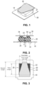
- FIG. 7 is a view for explaining a change in antenna gain characteristics of a patch antenna due to a difference in the shape of the parasitic element of the patch antenna device according to the illustrated embodiment, which illustrates shape variations of the parasitic element.
- FIG. 1 is a schematic perspective view for explaining a patch antenna device according to one illustrated embodiment.
- FIG. 2 is a schematic cross-sectional side view for explaining the patch antenna device according to the illustrated embodiment.
- FIG. 3 is a schematic top view for explaining the patch antenna device according to the illustrated embodiment.
- the same reference numerals as those in FIG. 1 denote the same parts as those in FIG. 1 .
- the patch antenna device according to the illustrated embodiment is configured to receive a radio communication signal.
- the patch antenna device according to the present disclosure mainly includes a circuit board 10 , a patch antenna 20 , and a parasitic element 30 .
- the circuit board 10 is a member on which a signal processing circuit is placed. A circuit pattern and a ground conductor pattern are formed by etching on the circuit board 10 . An amplifier circuit 14 and the like may also be placed on the circuit board 10 .
- the patch antenna 20 is placed on the circuit board 10 .
- the patch antenna 20 has a radiation element 22 having, e.g., a quadrangular shape.
- the illustrated patch antenna 20 is a ceramic patch antenna; however, the patch antenna according to the present invention is not limited to this, but may be an air-patch antenna using air as a dielectric, or may be a patch antenna using a synthetic resin as a dielectric or a patch antenna using a multilayer substrate as a dielectric.
- the patch antenna 20 is configured to receive signals in a frequency band for, e.g., SDARS, which is, specifically, 2.3 GHz band; however, the frequency band supported by the patch antenna 20 of the patch antenna device according to the present invention is not limited to the above frequency band and may be another frequency band.
- the patch antenna 20 includes a power feed line 21 and a radiation element 22 .
- the power feed line 21 is connected to a first power feed portion 11 of the circuit board 10 .
- a ceramic 23 is used as a dielectric.
- a ground conductor pattern 24 is provided on the back surface of the ceramic 23 , thereby constituting a micro-strip antenna together with the radiation element 22 .
- the patch antenna 20 is fixed onto the circuit board 10 by, e.g., a double-sided adhesive tape 25 .
- the parasitic element 30 is used for improving antenna gain characteristics of the patch antenna 20 .
- the parasitic element 30 is disposed above the patch antenna 20 .
- the parasitic element 30 is, e.g., a flat plate-like body.
- the parasitic element 30 is, e.g., made of a conductive plate.
- the parasitic element 30 is disposed parallel to and opposite to the radiation surface of the radiation element 22 of the patch antenna 20 .
- the length (e.g., “first length”) of the upper side of the parasitic element 30 is shorter than the width (e.g., “First Width”) in a plan view of the radiation element 22 of the patch antenna 20 .
- the length (e.g., “Second Length”) between the upper and lower sides of the parasitic element 30 is longer than the length (e.g., “Third Length”) between the upper and lower sides of the radiation element 22 of the patch antenna 20 .
- the parasitic element 30 of the patch antenna device according to the present disclosure is, e.g., a hexagonal plate-like body as illustrated.
- the parasitic element 30 has a hexagonal shape having two opposing parallel left and right sides, a lower side perpendicular to the two sides, and an upper side shorter than the lower side and parallel to the lower side. Further, as illustrated in FIG. 3 , the parasitic element 30 is disposed such that the center thereof overlaps the center of patch antenna 20 in a plan view.
- the parasitic element 30 is disposed above the patch antenna 20 with an insulating spacer 50 interposed therebetween.
- the insulating spacer 50 is disposed between the patch antenna 20 and the parasitic element 30 so as to support the parasitic element 30 .
- the patch antenna device has the parasitic element functioning as a wave director for the patch antenna and contributing to a size reduction and an increase in design freedom. That is, the length of the upper side of the parasitic element is shorter than the width of the patch antenna, so that the parasitic element for improving antenna gain characteristics can be disposed in a tapered area of the tip of a so-called shark-fin antenna. Further, the parasitic element having a flat plate-like shape is disposed parallel to and opposite to the radiation surface of the radiation element of the patch antenna, whereby the thickness of the entire patch antenna device can be reduced.
- the patch antenna device uses one patch antenna; however, the present disclosure can be applied to a stacked patch antenna device having a stacking structure using a plurality of patch antennas.
- FIG. 4 is a schematic cross-sectional side view for explaining a configuration obtained by applying the patch antenna device according to the illustrated disclosure to a stacked patch antenna device.
- the same reference numerals as those in FIG. 1 denote the same parts as those in FIG. 1 .
- a first patch antenna 20 a and a second patch antenna 20 b are provided as the patch antenna.
- the first patch antenna 20 a is stacked on the circuit board 10 and configured to receive signals in a first frequency band.
- the first frequency band may be a frequency band for, e.g., GNSS, which ranges from 1 GHz to 2 GHz; however, the frequency band supported by the first patch antenna 20 a of the patch antenna device according to the present invention is not limited to the above frequency band and may be another frequency band.
- the first patch antenna 20 a includes a first power feed line 21 a and a first radiation element 22 a .
- the first power feed line 21 a is connected to the first power feed portion 11 of the circuit board 10 .
- the first patch antenna 20 a is fixed onto the circuit board 10 by, e.g., a double-sided adhesive tape 25 a .
- the first patch antenna 20 a is a ceramic patch antenna using a ceramic 23 a as a dielectric; however, the first patch antenna 20 a of the patch antenna device according to the present invention is not limited to this, but may be an air-patch antenna using air as a dielectric, a patch antenna using a synthetic resin as a dielectric, or a patch antenna using a multilayer substrate as a dielectric.
- the second patch antenna 20 b is stacked on the first patch antenna 20 a and configured to receive signals in a second frequency band.
- the second frequency band may be a frequency band for, e.g., SDARS, which is, specifically, 2.3 GHz band; however, the frequency band supported by the second patch antenna 20 b of the patch antenna device according to the present invention is not limited to the above frequency band and may be another frequency band which is higher than the first frequency band.
- the second patch antenna 20 b includes a second power feed line 21 b and a second radiation element 22 b .
- the second power feed line 21 b is connected to a second power feed portion 12 of the circuit board 10 .
- the second patch antenna 20 b is fixed onto the first patch antenna 20 a by, e.g., a double-sided adhesive tape 25 b .
- the second patch antenna 20 b is a ceramic patch antenna using a ceramic 23 b as a dielectric; however, the second patch antenna 20 b of the patch antenna device according to the present invention is not limited to this, but may be an air-patch antenna using air as a dielectric, a patch antenna using a synthetic resin as a dielectric, or a patch antenna using a multilayer substrate as a dielectric.
- the parasitic element 30 is disposed above the second patch antenna 20 b and used for improving antenna gain characteristics of the second patch antenna 20 b .
- the length (e.g., “First Length”) of the upper side of the parasitic element 30 is shorter than the width (e.g., “Second Width”) in a plan view of the radiation element 22 b of the second patch antenna 20 b
- the length (e.g., “Second Length”) between the upper and lower sides of the parasitic element 30 is longer than the length (“Fourth Length”) between the upper and lower sides of the radiation element 22 b of the second patch antenna 20 b.
- the parasitic element 30 is supported by the insulating spacer 50 ; however, the present invention is not limited to this.
- the parasitic element may be supported by an integrated resin holder.
- FIG. 5 is a schematic perspective view for explaining another stacked patch antenna device to which the patch antenna device according to the illustrated disclosure is applied.
- the same reference numerals as those in FIG. 1 denote the same parts as those in FIG. 1 .
- the parasitic element 30 is supported by an integrated resin holder 40 .
- the integrated resin holder 40 supports the circuit board 10 , the first patch antenna 20 a , and the parasitic element 30 .
- the illustrated first patch antenna 20 a is a plate-like air patch antenna; however, the patch antenna according to the present invention is not limited to this, but may be a patch antenna using, as a dielectric, a ceramic, a synthetic resin, or a multilayer substrate.
- the circuit board 10 has a ground conductor pattern.
- the ground conductor pattern constitutes a micro-strip antenna together with the first radiation element 22 a .
- the illustrated first radiation element 22 a is a quadrangular plate-like element and is disposed opposite to the circuit board 10 with a predetermined interval therefrom.
- the power feed line 21 a is formed by cutting and bending a part of the radiation surface of the quadrangular plate-like element.
- FIG. 6 is a schematic top view for explaining the parasitic element of the patch antenna device according to the illustrated disclosure.
- the same reference numerals as those in FIG. 1 denote the same parts as those in FIG. 1 .
- the upward direction in FIG. 6 corresponds to a vehicle travel direction and to the tip side of the shark-fin antenna.
- the parasitic element 30 of the patch antenna device according to the present disclosure has held portions 31 , 32 having at least two sides opposed to each other.
- the parasitic element 30 has a hexagonal plate-like body as illustrated.
- the held portions 31 , 32 of the parasitic element 30 are formed in the opposing parallel upper and lower sides, respectively.
- the parasitic element 30 has a hexagonal shape having two opposing left and right sides, a lower side perpendicular to the two sides, and an upper side shorter than the lower side and parallel to the lower side.
- the held portions 31 , 32 of the parasitic element 30 are configured as parasitic element locking concaves that parasitic element locking pawls 41 , 42 of the integrated resin holder 40 lock. That is, the bottom sides of the parasitic element locking concaves of the held portions are the two opposing parallel sides.
- the presence of the parasitic element locking concaves of the held portions 31 , 32 allows the position of the parasitic element 30 with respect to the second patch antenna 20 b to be accurately fixed. Details of the parasitic element locking concaves of the held portions 31 , 32 will be described later.
- the shape of the parasitic element 30 is not limited to a hexagon and may be, for example, a trapezoid. Specifically, the trapezoid may be a quadrangle having the upper side shorter than the lower side and parallel to the lower side.
- the integrated resin holder 40 is a member for supporting the circuit board 10 and the parasitic element 30 .
- the integrated resin holder 40 has at least a pair of parasitic element locking pawls 41 , 42 .
- the parasitic element locking pawls 41 , 42 support the two sides of the held portions 31 , 32 of the parasitic element 30 so as to sandwich the parasitic element 30 from both sides in the horizontal direction such that the distance between the second patch antenna 20 b and the parasitic element 30 is kept constant.
- the integrated resin holder 40 is made of insulating resin.
- the parasitic element locking pawls 41 , 42 each pinch the front and back surfaces of the parasitic element 30 so as to keep the position of the parasitic element 30 in the height direction constant.
- the integrated resin holder 40 may further have a plate support portion 45 that is disposed between the plate-like air patch antenna and the circuit board 10 and supports the plate-like air patch antenna. That is, the integrated resin holder 40 may be configured to support also the first radiation element 22 a of the plate-like air patch antenna.
- the use of the plate support portion 45 can prevent the first radiation element 22 a of the first patch antenna 20 a from being bent due to vibration or the like. Further, bosses 49 protrude from the plate support portion 45 of the integrated resin holder 40 .
- the bosses 49 are inserted into fixing holes formed in the first patch antenna 20 a for thermal welding, whereby the first patch antenna 20 a is fixed to the integrated resin holder 40 .
- the first patch antenna 20 a may be fixed to the integrated resin holder 40 by means of screws.
- the integrated resin holder 40 has the plate support portion 45 as a center component and further has the parasitic element locking pawls 41 , 42 and the circuit board locking pawls 46 , 47 on the upper and lower sides of the plate support portion 45 , respectively.
- the parasitic element locking pawls 41 , 42 extend from the plate support portion 45 toward the parasitic element 30 to hold the parasitic element 30 .
- the parasitic element locking pawls 41 , 42 lock the held portions 31 , 32 formed in the upper and lower sides of the parasitic element 30 having, e.g., a hexagonal shape as illustrated in FIG. 6 so as to pinch them.
- the held portions 31 , 32 of the parasitic element 30 are configured as the parasitic element locking concaves that the parasitic element locking pawls 41 , 42 lock. That is, the parasitic element 30 has concaves as the held portions at positions corresponding to the parasitic element locking pawls 41 , 42 .
- the parasitic element locking pawl 42 which is one of the parasitic element locking pawls that support the held portions 31 , 32 having two opposing parallel sides of the parasitic element 30 so as to sandwich the parasitic element 30 from both sides in the horizontal direction, includes two side-by-side locking pawls 43 , 44 .
- the held portion 32 of the parasitic element 30 includes side-by-side locking concaves 33 , 34 .
- the side-by-side locking concaves 33 , 34 are locked by the side-by-side locking pawls 43 , 44 , respectively.
- the side-by-side locking concaves 33 , 34 each preferably have a right-trapezoidal concave having an opening width larger than the width of each locking pawl and having an opening bottom width smaller than the width of each locking pawl. Further, the right-angled portions of the right-trapezoidal concaves of the respective side-by-side locking concaves 33 , 34 are preferably positioned on a side close to each of the side-by-side locking concaves 33 , 34 , respectively. The oblique sides are preferably positioned on a side far from each of the side-by-side locking concaves 33 , 34 , respectively.
- the right-angled portion of the locking concave 33 is positioned at the corner close to the locking concave 34
- the right-angled portion of the locking concave 34 is positioned at the corner close to the locking concave 33 .
- FIG. 7 is a view for explaining a change in the antenna gain characteristics of the patch antenna due to a difference in the shape of the parasitic element of the patch antenna device according to the present disclosure, which illustrates shape variations of the parasitic element. Measurement was made using the configuration of the patch antenna device illustrated in FIG. 1 under the following conditions. The size of the radiation element of the patch antenna was 25 mm ⁇ 25 mm. The distance between the radiation element of the patch antenna and the parasitic element was 3 mm. Parasitic elements of five different shapes illustrated in FIG. 7 were used.
- the five different shapes were (1) hexagon (a) (lower side: 25 mm, height: 32 mm), (2) trapezoid (lower side: 30 mm, height: 32 mm), (3) triangle (lower side: 30 mm, height 32 mm), (4) square (lower side: 32 mm, height: 32 mm), and (5) hexagon (b) (lower side: 25 mm, height: 27 mm).
- hexagon (a) lower side: 25 mm, height: 32 mm
- trapezoid lower side: 30 mm, height: 32 mm
- triangle lower side: 30 mm, height 32 mm
- (4) square lower side: 32 mm, height: 32 mm
- hexagon (b) lower side: 25 mm, height: 27 mm
- the parasitic elements having (1) hexagonal shape (a) and (2) trapezoidal shape are high in the horizontal plane average gain and are suitable examples. Further, the horizontal plane average gain is higher in the case where the length between the upper and lower sides is long as in (1) hexagon (a) than in the case where the length between the upper and lower sides is short as in (5) hexagon (b). Further, the horizontal plane average gain becomes low in an extremely pointed shape like (3) triangle having no upper side.
- the parasitic element of the patch antenna device according to the present disclosure is preferably configured such that the length of the upper side is shorter than the width in a plan view of the radiation element of the patch antenna and that the length between the upper and lower sides is longer than the length between the upper and lower sides of the radiation element of the patch antenna.
- the patch antenna device according to the present invention is not limited to the above illustrated examples but may be variously modified without departing from the scope of the present invention.
Landscapes
- Engineering & Computer Science (AREA)
- Remote Sensing (AREA)
- Physics & Mathematics (AREA)
- Electromagnetism (AREA)
- Computer Security & Cryptography (AREA)
- Radar, Positioning & Navigation (AREA)
- Waveguide Aerials (AREA)
- Variable-Direction Aerials And Aerial Arrays (AREA)
- Details Of Aerials (AREA)
Abstract
Description
| TABLE 1 | |||||
| Hexagon (a) | Trapezoid | Triangle | Hexagon (b) | Square | |
| Horizontal | −10.8 | −11.1 | −12.0 | −12.2 | −12.6 |
| plane average | |||||
| gain (dB) | |||||
Claims (6)
Applications Claiming Priority (3)
| Application Number | Priority Date | Filing Date | Title |
|---|---|---|---|
| JP2019-186574 | 2019-10-10 | ||
| JPJP2019-186574 | 2019-10-10 | ||
| JP2019186574A JP6935474B2 (en) | 2019-10-10 | 2019-10-10 | Patch antenna device |
Publications (2)
| Publication Number | Publication Date |
|---|---|
| US20210111491A1 US20210111491A1 (en) | 2021-04-15 |
| US11569578B2 true US11569578B2 (en) | 2023-01-31 |
Family
ID=75383207
Family Applications (1)
| Application Number | Title | Priority Date | Filing Date |
|---|---|---|---|
| US17/061,100 Active US11569578B2 (en) | 2019-10-10 | 2020-10-01 | Patch antenna device |
Country Status (2)
| Country | Link |
|---|---|
| US (1) | US11569578B2 (en) |
| JP (1) | JP6935474B2 (en) |
Cited By (1)
| Publication number | Priority date | Publication date | Assignee | Title |
|---|---|---|---|---|
| US20250337169A1 (en) * | 2024-04-30 | 2025-10-30 | Aptiv Technologies AG | Combined Air Waveguide Antenna and Housing |
Families Citing this family (6)
| Publication number | Priority date | Publication date | Assignee | Title |
|---|---|---|---|---|
| JP6921917B2 (en) * | 2019-10-01 | 2021-08-18 | 原田工業株式会社 | Antenna module |
| KR102650820B1 (en) * | 2019-11-18 | 2024-03-26 | 삼성전자주식회사 | Antenna and electronic device incluidng the same |
| KR102661303B1 (en) * | 2020-01-13 | 2024-04-30 | 엘지전자 주식회사 | Antenna system mounted on vehicle |
| DE102022203585A1 (en) * | 2022-04-08 | 2023-10-12 | Continental Automotive Technologies GmbH | Multi-layer patch antenna device, antenna module and vehicle with a multi-layer patch antenna device |
| EP4318806B1 (en) * | 2022-08-01 | 2024-07-10 | Sick Ag | Modular antenna for an rfid reader |
| CN116742329A (en) * | 2023-06-29 | 2023-09-12 | 昆山睿翔讯通通信技术有限公司 | A circularly polarized millimeter wave antenna and terminal |
Citations (6)
| Publication number | Priority date | Publication date | Assignee | Title |
|---|---|---|---|---|
| US20100171675A1 (en) * | 2007-06-06 | 2010-07-08 | Carmen Borja | Dual-polarized radiating element, dual-band dual-polarized antenna assembly and dual-polarized antenna array |
| JP2013183388A (en) | 2012-03-03 | 2013-09-12 | Kanazawa Inst Of Technology | Microstrip antenna having circular polarization characteristics |
| US20150194730A1 (en) * | 2012-09-21 | 2015-07-09 | Murata Manufacturing Co., Ltd. | Dual-polarized antenna |
| US20190020114A1 (en) * | 2017-07-14 | 2019-01-17 | Apple Inc. | Millimeter Wave Patch Antennas |
| JP2019016930A (en) | 2017-07-07 | 2019-01-31 | 株式会社ヨコオ | Antenna device |
| US20190280386A1 (en) * | 2018-03-08 | 2019-09-12 | Yokowo Co., Ltd. | Patch antenna |
Family Cites Families (5)
| Publication number | Priority date | Publication date | Assignee | Title |
|---|---|---|---|---|
| JP4789532B2 (en) * | 2004-09-27 | 2011-10-12 | 日本無線株式会社 | Circularly polarized patch antenna and circularly polarized array antenna |
| JP4562611B2 (en) * | 2005-07-29 | 2010-10-13 | 日本無線株式会社 | Circularly polarized patch antenna and circularly polarized array antenna |
| KR100988909B1 (en) * | 2008-09-23 | 2010-10-20 | 한국전자통신연구원 | Microstrip Patch Antenna with High Gain and Wideband Characteristics |
| JP2017191961A (en) * | 2016-04-11 | 2017-10-19 | 三菱電機株式会社 | Antenna device |
| JP7009031B2 (en) * | 2017-12-05 | 2022-01-25 | 日本無線株式会社 | Circularly polarized shared plane antenna |
-
2019
- 2019-10-10 JP JP2019186574A patent/JP6935474B2/en active Active
-
2020
- 2020-10-01 US US17/061,100 patent/US11569578B2/en active Active
Patent Citations (7)
| Publication number | Priority date | Publication date | Assignee | Title |
|---|---|---|---|---|
| US20100171675A1 (en) * | 2007-06-06 | 2010-07-08 | Carmen Borja | Dual-polarized radiating element, dual-band dual-polarized antenna assembly and dual-polarized antenna array |
| JP2013183388A (en) | 2012-03-03 | 2013-09-12 | Kanazawa Inst Of Technology | Microstrip antenna having circular polarization characteristics |
| US20150194730A1 (en) * | 2012-09-21 | 2015-07-09 | Murata Manufacturing Co., Ltd. | Dual-polarized antenna |
| JP2019016930A (en) | 2017-07-07 | 2019-01-31 | 株式会社ヨコオ | Antenna device |
| US20190020114A1 (en) * | 2017-07-14 | 2019-01-17 | Apple Inc. | Millimeter Wave Patch Antennas |
| US20190280386A1 (en) * | 2018-03-08 | 2019-09-12 | Yokowo Co., Ltd. | Patch antenna |
| JP2019161312A (en) | 2018-03-08 | 2019-09-19 | 株式会社ヨコオ | Patch antenna |
Cited By (1)
| Publication number | Priority date | Publication date | Assignee | Title |
|---|---|---|---|---|
| US20250337169A1 (en) * | 2024-04-30 | 2025-10-30 | Aptiv Technologies AG | Combined Air Waveguide Antenna and Housing |
Also Published As
| Publication number | Publication date |
|---|---|
| JP6935474B2 (en) | 2021-09-15 |
| US20210111491A1 (en) | 2021-04-15 |
| JP2021064821A (en) | 2021-04-22 |
Similar Documents
| Publication | Publication Date | Title |
|---|---|---|
| US11569578B2 (en) | Patch antenna device | |
| US11309631B2 (en) | Stacked patch antenna | |
| US11228109B2 (en) | Antenna device | |
| US20080055184A1 (en) | Antenna device, antenna element and antenna module | |
| JP2018121143A (en) | Composite antenna device | |
| US8947309B2 (en) | Antenna device and display device | |
| CN116636088A (en) | Chip Antenna and Vehicle Antenna Device | |
| US11196154B2 (en) | Antenna device | |
| JP6825013B2 (en) | Vehicle antenna | |
| US11342675B2 (en) | Antenna module | |
| KR102487335B1 (en) | Lightweight patch antenna | |
| JP6181498B2 (en) | Antenna device | |
| US20220368030A1 (en) | Antenna device and communication device | |
| US20040201523A1 (en) | Patch antenna apparatus preferable for receiving ground wave and signal wave from low elevation angle satellite | |
| WO2024225038A1 (en) | Antenna device, antenna, and vehicle | |
| JP3764289B2 (en) | Microstrip antenna | |
| US12046840B2 (en) | Antenna structure | |
| US12573769B2 (en) | Antenna device | |
| JP2002299949A (en) | Planar array antenna | |
| US12095154B2 (en) | Antenna structure | |
| US12088025B2 (en) | Antenna structure | |
| US20250055181A1 (en) | Patch antenna and antenna device | |
| JP2005051683A (en) | Combined antenna | |
| JPH0661735A (en) | Planar antenna | |
| JP3017553B2 (en) | Planar antenna |
Legal Events
| Date | Code | Title | Description |
|---|---|---|---|
| AS | Assignment |
Owner name: HARADA INDUSTRY CO., LTD., JAPAN Free format text: ASSIGNMENT OF ASSIGNORS INTEREST;ASSIGNOR:HASEGAWA, RYOHEI;REEL/FRAME:053952/0199 Effective date: 20201001 |
|
| FEPP | Fee payment procedure |
Free format text: ENTITY STATUS SET TO UNDISCOUNTED (ORIGINAL EVENT CODE: BIG.); ENTITY STATUS OF PATENT OWNER: LARGE ENTITY |
|
| STPP | Information on status: patent application and granting procedure in general |
Free format text: APPLICATION DISPATCHED FROM PREEXAM, NOT YET DOCKETED |
|
| STPP | Information on status: patent application and granting procedure in general |
Free format text: DOCKETED NEW CASE - READY FOR EXAMINATION |
|
| STPP | Information on status: patent application and granting procedure in general |
Free format text: NON FINAL ACTION MAILED |
|
| STPP | Information on status: patent application and granting procedure in general |
Free format text: RESPONSE TO NON-FINAL OFFICE ACTION ENTERED AND FORWARDED TO EXAMINER |
|
| STPP | Information on status: patent application and granting procedure in general |
Free format text: FINAL REJECTION MAILED |
|
| STPP | Information on status: patent application and granting procedure in general |
Free format text: DOCKETED NEW CASE - READY FOR EXAMINATION |
|
| STPP | Information on status: patent application and granting procedure in general |
Free format text: NOTICE OF ALLOWANCE MAILED -- APPLICATION RECEIVED IN OFFICE OF PUBLICATIONS |
|
| STPP | Information on status: patent application and granting procedure in general |
Free format text: PUBLICATIONS -- ISSUE FEE PAYMENT RECEIVED |
|
| STPP | Information on status: patent application and granting procedure in general |
Free format text: PUBLICATIONS -- ISSUE FEE PAYMENT VERIFIED |
|
| STCF | Information on status: patent grant |
Free format text: PATENTED CASE |