US11515449B2 - Semiconductor light emitting device and method of fabricating the same - Google Patents
Semiconductor light emitting device and method of fabricating the same Download PDFInfo
- Publication number
- US11515449B2 US11515449B2 US16/935,356 US202016935356A US11515449B2 US 11515449 B2 US11515449 B2 US 11515449B2 US 202016935356 A US202016935356 A US 202016935356A US 11515449 B2 US11515449 B2 US 11515449B2
- Authority
- US
- United States
- Prior art keywords
- light emitting
- electrode
- layer
- semiconductor
- opening
- Prior art date
- Legal status (The legal status is an assumption and is not a legal conclusion. Google has not performed a legal analysis and makes no representation as to the accuracy of the status listed.)
- Active, expires
Links
Images


Classifications
-
- H—ELECTRICITY
- H10—SEMICONDUCTOR DEVICES; ELECTRIC SOLID-STATE DEVICES NOT OTHERWISE PROVIDED FOR
- H10H—INORGANIC LIGHT-EMITTING SEMICONDUCTOR DEVICES HAVING POTENTIAL BARRIERS
- H10H20/00—Individual inorganic light-emitting semiconductor devices having potential barriers, e.g. light-emitting diodes [LED]
- H10H20/80—Constructional details
- H10H20/83—Electrodes
- H10H20/831—Electrodes characterised by their shape
- H10H20/8316—Multi-layer electrodes comprising at least one discontinuous layer
-
- H—ELECTRICITY
- H10—SEMICONDUCTOR DEVICES; ELECTRIC SOLID-STATE DEVICES NOT OTHERWISE PROVIDED FOR
- H10H—INORGANIC LIGHT-EMITTING SEMICONDUCTOR DEVICES HAVING POTENTIAL BARRIERS
- H10H20/00—Individual inorganic light-emitting semiconductor devices having potential barriers, e.g. light-emitting diodes [LED]
- H10H20/80—Constructional details
- H10H20/83—Electrodes
- H10H20/831—Electrodes characterised by their shape
-
- H01L33/387—
-
- H01L33/62—
-
- H—ELECTRICITY
- H10—SEMICONDUCTOR DEVICES; ELECTRIC SOLID-STATE DEVICES NOT OTHERWISE PROVIDED FOR
- H10H—INORGANIC LIGHT-EMITTING SEMICONDUCTOR DEVICES HAVING POTENTIAL BARRIERS
- H10H20/00—Individual inorganic light-emitting semiconductor devices having potential barriers, e.g. light-emitting diodes [LED]
- H10H20/01—Manufacture or treatment
-
- H—ELECTRICITY
- H10—SEMICONDUCTOR DEVICES; ELECTRIC SOLID-STATE DEVICES NOT OTHERWISE PROVIDED FOR
- H10H—INORGANIC LIGHT-EMITTING SEMICONDUCTOR DEVICES HAVING POTENTIAL BARRIERS
- H10H20/00—Individual inorganic light-emitting semiconductor devices having potential barriers, e.g. light-emitting diodes [LED]
- H10H20/80—Constructional details
- H10H20/81—Bodies
- H10H20/819—Bodies characterised by their shape, e.g. curved or truncated substrates
- H10H20/821—Bodies characterised by their shape, e.g. curved or truncated substrates of the light-emitting regions, e.g. non-planar junctions
-
- H—ELECTRICITY
- H10—SEMICONDUCTOR DEVICES; ELECTRIC SOLID-STATE DEVICES NOT OTHERWISE PROVIDED FOR
- H10H—INORGANIC LIGHT-EMITTING SEMICONDUCTOR DEVICES HAVING POTENTIAL BARRIERS
- H10H20/00—Individual inorganic light-emitting semiconductor devices having potential barriers, e.g. light-emitting diodes [LED]
- H10H20/80—Constructional details
- H10H20/83—Electrodes
- H10H20/831—Electrodes characterised by their shape
- H10H20/8312—Electrodes characterised by their shape extending at least partially through the bodies
-
- H—ELECTRICITY
- H10—SEMICONDUCTOR DEVICES; ELECTRIC SOLID-STATE DEVICES NOT OTHERWISE PROVIDED FOR
- H10H—INORGANIC LIGHT-EMITTING SEMICONDUCTOR DEVICES HAVING POTENTIAL BARRIERS
- H10H20/00—Individual inorganic light-emitting semiconductor devices having potential barriers, e.g. light-emitting diodes [LED]
- H10H20/80—Constructional details
- H10H20/85—Packages
- H10H20/857—Interconnections, e.g. lead-frames, bond wires or solder balls
-
- H—ELECTRICITY
- H10—SEMICONDUCTOR DEVICES; ELECTRIC SOLID-STATE DEVICES NOT OTHERWISE PROVIDED FOR
- H10H—INORGANIC LIGHT-EMITTING SEMICONDUCTOR DEVICES HAVING POTENTIAL BARRIERS
- H10H29/00—Integrated devices, or assemblies of multiple devices, comprising at least one light-emitting semiconductor element covered by group H10H20/00
- H10H29/10—Integrated devices comprising at least one light-emitting semiconductor component covered by group H10H20/00
- H10H29/14—Integrated devices comprising at least one light-emitting semiconductor component covered by group H10H20/00 comprising multiple light-emitting semiconductor components
- H10H29/142—Two-dimensional arrangements, e.g. asymmetric LED layout
-
- H01L2933/0016—
-
- H—ELECTRICITY
- H10—SEMICONDUCTOR DEVICES; ELECTRIC SOLID-STATE DEVICES NOT OTHERWISE PROVIDED FOR
- H10H—INORGANIC LIGHT-EMITTING SEMICONDUCTOR DEVICES HAVING POTENTIAL BARRIERS
- H10H20/00—Individual inorganic light-emitting semiconductor devices having potential barriers, e.g. light-emitting diodes [LED]
- H10H20/01—Manufacture or treatment
- H10H20/032—Manufacture or treatment of electrodes
Definitions
- Apparatuses, devices, and methods consistent with the present disclosure relate to a semiconductor light emitting device and a method of fabricating the same.
- LED light emitting diodes
- LED Semiconductor light emitting devices, such as light emitting diodes
- LED are apparatuses in which light is released from materials included therein.
- Light emitting devices emit light converted from energy generated from recombination of electrons and holes contained in combined semiconductors.
- Such light emitting diodes (LED) are currently in widespread use as illumination, display devices, and light sources, and development thereof have been accelerated.
- a semiconductor light emitting device comprising a light emitting structure that includes a first semiconductor layer, an active layer, and a second semiconductor layer that are sequentially stacked, and that includes a first opening that penetrates the second semiconductor layer and the active layer, the first opening exposing the first semiconductor layer; a first electrode that fills at least a portion of the first opening; a first dielectric layer on the first electrode; a second electrode on the light emitting structure and covering the first dielectric layer, the second electrode being electrically connected to the second semiconductor layer; and a vertical conductive pattern that surrounds outer lateral surfaces of the light emitting structure and is electrically connected to the first electrode.
- a semiconductor light emitting device comprising a light emitting structure that includes a first semiconductor layer, an active layer, and a second semiconductor layer that are sequentially stacked; a first opening that penetrates the second semiconductor layer and the active layer, the first opening exposing the first semiconductor layer; a first electrode that partially fills the first opening and contacts the first semiconductor layer exposed by the first opening; a second electrode that covers the second semiconductor layer and the first electrode; and a first dielectric layer between the first electrode and the second electrode.
- a method of fabricating a semiconductor light emitting device comprising sequentially stacking a first semiconductor layer, an active layer, and a second semiconductor layer to form a light emitting structure on a growth substrate; removing a portion of the light emitting structure that is spaced apart from outer lateral surfaces of the light emitting structure to form an opening that exposes the first semiconductor layer; filling a lower portion of the opening with a conductive material to form a first electrode; filling a remaining portion of the opening with a dielectric material to form a first dielectric layer; and coating a conductive material on the second semiconductor layer and the first dielectric layer to form a second electrode.
- FIG. 1 illustrates a plan view showing a semiconductor light emitting device according to some example embodiments
- FIGS. 2A and 2B illustrate cross-sectional views showing a semiconductor light emitting device according to some example embodiments
- FIGS. 3 and 4 illustrate cross-sectional views showing a semiconductor light emitting device according to some example embodiments
- FIGS. 5 and 6 illustrate cross-sectional views showing a semiconductor light emitting device according to some example embodiments
- FIG. 7 illustrates a plan view showing a semiconductor light emitting device according to some example embodiments
- FIG. 8 illustrates a cross-sectional view showing a semiconductor light emitting device according to some example embodiments
- FIG. 9 illustrates a plan view showing a method of fabricating a semiconductor light emitting device array according to some example embodiments.
- FIG. 10 illustrates a circuit diagram showing a semiconductor light emitting device array according to some example embodiments
- FIGS. 11A to 23A and 11B to 23B illustrate cross-sectional views showing a method of fabricating a semiconductor light emitting device array according to some example embodiments
- FIG. 24 illustrates a plan view showing a method of fabricating a semiconductor light emitting device array according to some example embodiments.
- FIGS. 25 and 26 illustrate cross-sectional views showing a method of fabricating a semiconductor light emitting device array according to some example embodiments.
- FIG. 1 illustrates a plan view showing a semiconductor light emitting device according to some example embodiments.
- FIGS. 2A and 2B illustrate cross-sectional views taken along line A-A′ of FIG. 1 , showing a semiconductor light emitting device according to some example embodiments.
- FIGS. 3 and 4 illustrate cross-sectional views showing a semiconductor light emitting device according to some example embodiments.
- a semiconductor light emitting device 10 may include a growth substrate 100 and a light emitting structure 110 that includes a first semiconductor layer 112 , an active layer 114 , and a second semiconductor layer 116 that are sequentially stacked on the growth substrate 100 .
- a buffer layer (not shown) may be interposed between the growth substrate 100 and the first semiconductor layer 112 .
- the buffer layer (not shown) may be provided to alleviate a lattice mismatch between the growth substrate 100 and the first semiconductor layer 112 .
- the growth substrate 100 may be a transparent substrate, such as a sapphire substrate.
- the growth substrate 100 may be an opaque substrate, such as a silicon (Si) substrate.
- the first semiconductor layer 112 may include a semiconductor doped with n-type impurities.
- the first semiconductor layer 112 may be an n-type semiconductor nitride layer.
- the second semiconductor layer 116 may include a semiconductor doped with p-type impurities.
- the second semiconductor layer 116 may be a p-type semiconductor nitride layer.
- the first and second semiconductor layers 112 and 116 may have a composition of Al x In y Ga (1-x-y) N (where, 0 ⁇ x ⁇ 1, 0 ⁇ y ⁇ 1, 0 ⁇ x+y ⁇ 1).
- the first and second semiconductor layers 112 and 116 may include GaN, AlGaN, InGaN, or AlInGaN.
- the n-type impurities may include silicon (Si)
- the p-type impurities may include magnesium (Mg).
- the active layer 114 may be disposed between the first and second semiconductor layers 112 and 116 , and may discharge light whose energy is generated by recombination of electron-hole.
- the active layer 114 may include a material whose energy bandgap is less than that of materials of the first and second semiconductor layers 112 and 116 .
- the active layer 114 may include an InGaN-based compound semiconductor whose energy bandgap is less than that of GaN.
- the active layer 114 may have a multiple quantum well (MQW) structure, such as a structure of InGaN/GaN, in which at least one quantum well layer and at least one quantum barrier layer are alternately stacked.
- MQW multiple quantum well
- the active layer 114 may have a single quantum well (SQW) structure.
- the light emitting structure 110 may include a first region R 1 and a second region R 2 .
- the first region R 1 may correspond to an area where the second semiconductor layer 116 and the active layer 114 are etched to expose a top surface of the first semiconductor layer 112 .
- the second region R 2 may correspond to an area of the light emitting structure 110 , which area is not etched during the formation of the first region R 1 . When viewed in plan, the second region R 2 may surround the first region R 1 as illustrated in FIG. 1 .
- the light emitting structure 110 may have a first opening OP 1 .
- the first opening OP 1 may be provided on the first region R 1 .
- the first opening OP 1 may penetrate the second semiconductor layer 116 and the active layer 114 of the light emitting structure 110 , and may expose the top surface of the first semiconductor layer 112 .
- the first opening OP 1 may be used as a connection path through which the first semiconductor layer 112 is coupled to a first electrode 120 which will be discussed below.
- the first opening OP 1 may have a tetragonal shape when viewed in plan as illustrated in FIG. 1 , but example embodiments are not limited thereto. In other example embodiments, the first opening OP 1 may have a circular or polygonal shape when viewed in plan. As shown in FIG. 2A , the first opening OP 1 may have a width that gradually decreases as approaching the growth substrate 100 . In other words, the width of the first opening OP 1 may gradually decrease as a distance from the growth substrate 100 decreases.
- the first opening OP 1 may have a minimum width less than about 10 ⁇ m. For example, the minimum width of the first opening OP 1 may range from about 0.1 ⁇ m to about 10 ⁇ m. A distance of about 1 ⁇ m to about 100 ⁇ m may be provided between an inner lateral surface of the first opening OP 1 and an outer lateral surface of the light emitting structure 110 .
- a first electrode 120 may be disposed in the first opening OP 1 .
- the first electrode 120 may fill a lower portion of the first opening OP 1 .
- the first electrode 120 may be in contact with bottom and inner lateral surfaces of the first opening OP 1 .
- the first electrode 120 may be in contact with top and lateral surfaces of the first semiconductor layer 112 that are exposed to the first opening OP 1 .
- the first electrode 120 and the top and lateral surfaces of the first semiconductor layer 112 that are exposed to the first opening OP 1 may be in contact with each other to form an n-contact.
- the n-contact may extend down one side surface of the first opening OP 1 across the bottom of the first opening OP 1 and up the other side surface of the first opening OP 1 .
- the first electrode 120 may be electrically connected through the n-contact to the first semiconductor layer 112 .
- the first electrode 120 may have a top surface at a lower level than that of a bottom surface of the active layer 114 . Therefore, the first electrode 120 may be spaced apart and electrically insulated from the active layer 114 and the second semiconductor layer 116 .
- the first electrode 120 may include a conductive material.
- the conductive material may include either metal such as copper (Cu), aluminum (Al), and silver (Ag) or transparent conductive oxide such as indium tin oxide (ITO), indium zinc oxide (IZO), and indium tin zinc oxide (ITZO).
- a first dielectric layer 130 may be disposed on the first electrode 120 .
- the first dielectric layer 130 may fill an upper portion of the first opening OP 1 .
- the first dielectric layer 130 may extend onto a top surface of the second semiconductor layer 116 on the second region R 2 .
- the first dielectric layer 130 may conformally cover the top surface of the second semiconductor layer 116 (except for where a second electrode 140 to be described later is provided), the inner lateral surface of the first opening OP 1 , and the top surface of the first electrode 120 .
- the first dielectric layer 130 may cover a lateral surface of the active layer 114 exposed to the inner lateral surface of the first opening OP 1 .
- the first dielectric layer 130 may include a dielectric material, such as silicon oxide or silicon nitride.
- the first dielectric layer 130 may have a structure in which a plurality of layers are alternately and repeatedly stacked, where the plurality of layers that have different refractive indices from each other that are less than a refractive index of the second semiconductor layer 116 .
- one of the plurality of layers may be a silicon oxide (SiO 2 ) layer
- another of the plurality of layers may be a titanium oxide (TiO 2 ) layer or a niobium oxide (Nb 2 O 5 ) layer.
- the first dielectric layer 130 may fill the upper portion of the first opening OP 1 , but may not extend onto the top surface of the second semiconductor layer 116 .
- the first dielectric layer 130 may have a top surface at a higher level than that of a top surface of the active layer 114 .
- the top surface of the first dielectric layer 130 may be located at the same level as that of the top surface of the second semiconductor layer 116 .
- the first dielectric layer 130 may have a second opening OP 2 that penetrates therethrough and exposes the top surface of the second semiconductor layer 116 .
- the second opening OP 2 may be located in the second region R 2 .
- the second opening OP 2 may be used as a connection path through which the second semiconductor layer 116 is coupled to a second electrode 140 which will be discussed below.
- a second electrode 140 may be disposed on the light emitting structure 110 .
- the second electrode 140 may be positioned on the first and second regions R 1 and R 2 .
- the second electrode 140 may cover the first dielectric layer 130 in the first region R 1 , and may extend onto the top surface of the second semiconductor layer 116 in the second region R 2 .
- the second electrode 140 may overlap an entirety of the first opening OP 1 and may have a planar shape larger than that of the first opening OP 1 .
- the second electrode 140 may have a planar shape that is larger than a planar shape of the first electrode 120 .
- the second electrode 140 may have a width greater than a maximum width of the first opening OP 1 .
- the second electrode 140 may be coupled to the second semiconductor layer 116 through the second opening OP 2 of the first dielectric layer 130 .
- the second electrode 140 may be in direct contact with the top surface of the second semiconductor layer 116 in the second region R 2 .
- the second electrode 140 may include a reflective metallic material, such as silver (Ag) or aluminum (A).
- the second electrode 140 may include silver (Ag).
- the second electrode 140 may be a multi-layered electrode.
- the second electrode 140 may include a transparent electrode layer 142 , an electrode dielectric layer 144 , and a reflective metal layer 146 that are sequentially stacked.
- the reflective metal layer 146 may be connected to the transparent electrode layer 142 through third openings OP 3 formed in the electrode dielectric layer 144 .
- the transparent electrode layer 142 may include a transparent conductive oxide, such as indium tin oxide (ITO), indium zinc oxide (IZO), and indium tin zinc oxide (ITZO).
- the electrode dielectric layer 144 may include a dielectric material whose refractive index less than that of a dielectric material of the second semiconductor layer 116 .
- the electrode dielectric layer 144 may be a single layer of silicon oxide (SiO 2 ).
- the electrode dielectric layer 144 may have a structure in which a plurality of layers are alternately and repeatedly stacked, where refractive indices of the layers are different from each other and less than a refractive index of the second semiconductor layer 116 .
- one of the plurality of layers may be a silicon oxide (SiO 2 ) layer, and another of the plurality of layers may be a titanium oxide (TiO 2 ) layer or a niobium oxide (Nb 2 O 5 ) layer.
- the electrode dielectric layer 144 may have an omnidirectional reflective (ODR) structure or a distributed Bragg reflective (DBR) structure.
- the reflective metal layer 146 may include a reflective metallic material, such as silver (Ag) or aluminum (Al).
- the second electrode 140 may be electrically connected to an external circuit through a conductive line, a solder bump, or a conductive plug provided on the second electrode 140 .
- the growth substrate 100 may be omitted (i.e., the growth substrate 100 may not be provided below the light emitting structure 110 ), and the first opening OP 1 may be formed to penetrate the light emitting structure 110 . Therefore, the first electrode 120 may be exposed on a bottom surface of the light emitting structure 110 , and may be electrically connected to an external circuit through a conductive line, a solder bump, or a conductive plug provided on an exposed bottom surface of the first electrode 120 .
- FIG. 3 the growth substrate 100 may be omitted (i.e., the growth substrate 100 may not be provided below the light emitting structure 110 ), and the first opening OP 1 may be formed to penetrate the light emitting structure 110 . Therefore, the first electrode 120 may be exposed on a bottom surface of the light emitting structure 110 , and may be electrically connected to an external circuit through a conductive line, a solder bump, or a conductive plug provided on an exposed bottom surface of the first electrode 120 .
- FIG. 3 the growth substrate 100 may be omitted (
- the growth substrate 100 may be omitted (i.e., the growth substrate 100 may not be provided below the light emitting structure 110 ), and the light emitting structure 110 may have a fourth opening OP 4 formed in a lower portion thereof.
- the fourth opening OP 4 may be provided in the first region R 1 .
- the fourth opening OP 4 may vertically overlap the first opening OP 1 , and may penetrate the first semiconductor layer 112 of the light emitting structure 110 and expose a bottom surface of the first electrode 120 .
- the fourth opening OP 4 may have a width less than that of a minimum width of the first opening OP 1 .
- a sub-electrode 122 may be disposed in the fourth opening OP 4 .
- the sub-electrode 122 may be coupled to the first electrode 120 .
- the sub-electrode 122 may be exposed on the bottom surface of the light emitting structure 110 , and may be electrically connected to an external circuit through a conductive line, a solder bump, or a conductive plug provided on an exposed bottom surface of the sub-electrode 122 .
- the light emitting structure when a first electrode and a second electrode for applying electrical signals to a light emitting structure are provided in different regions (i.e., the first electrode and the second electrode are provided in regions side-by-side), the light emitting structure must have a large area on which the first and second electrodes are disposed.
- the first and second electrodes 120 and 140 which apply electrical signals to the light emitting structure 110 , may vertically overlap each other. Therefore, the first and second electrodes 120 and 140 may be placed in a smaller area, and as a result the semiconductor light emitting device 10 may be easily reduced in size.
- the first electrode 120 may be buried in the first opening OP 1 of the light emitting structure 110 , and may be in contact with the top and lateral surfaces of the first semiconductor layer 112 exposed to the first opening OP 1 . Accordingly, the n-contact may have a large area between the first electrode 120 and the first semiconductor layer 112 , and the semiconductor light emitting device 10 may have improved electrical characteristics.
- the light emitting structure 110 may further have a recess positioned on the first opening OP 1 .
- FIGS. 5 and 6 illustrate cross-sectional views showing a semiconductor light emitting device according to some other example embodiments.
- a recess RS may be provided on the first region R 1 .
- the recess RS may penetrate the second semiconductor layer 116 and the active layer 114 , and may expose the first semiconductor layer 112 .
- the recess RS may be formed to vertically overlap the entirety of the first opening OP 1 .
- the recess RS may have a width greater than that of the first opening OP 1 , and also have a depth less than that of the first opening OP 1 .
- the depth of the recess RS may indicate a distance from the top surface of the second semiconductor layer 116 to a bottom surface of the recess RS, and the depth of the first opening OP 1 may denote a distance from the top surface of the second semiconductor layer 116 to a bottom surface of the first opening OP 1 .
- the first opening OP 1 may pass through a central portion of the recess RS and extend toward an inside of the first semiconductor layer 112 .
- the first electrode 120 may fill the lower portion of the first opening OP 1 , but may not fill the recess RS.
- the first dielectric layer 130 may fill the recess RS, and may extend onto the top surface of the second semiconductor layer 116 on the second region R 2 .
- the second electrode 140 may be disposed on the first dielectric layer 130 , and may be in contact with the second semiconductor layer 116 via the second opening OP 2 of the first dielectric layer 130 .
- a second dielectric layer 132 may be interposed between the first dielectric layer 130 and the second semiconductor layer 116 .
- the second dielectric layer 132 may cover the top surface of the second semiconductor layer 116 (except for an area of the second openings OP 2 ) and the bottom and inner lateral surfaces of the recess RS.
- the first opening OP 1 may be formed to penetrate the second dielectric layer 132 and to expose the first semiconductor layer 112
- the second opening OP 2 may be formed to penetrate the second dielectric layer 132 and to expose the second semiconductor layer 116 .
- the second dielectric layer 132 may include a dielectric material, such as silicon oxide or silicon nitride.
- the first electrode 120 may fill both the first opening OP 1 and the recess RS.
- the top surface of the first electrode 120 may be located at a higher level than that of the bottom surface of the active layer 114 .
- the top surface of the first electrode 120 may be positioned inside the recess RS or located at a higher level than that of the top surface of the second semiconductor layer 116 .
- the second dielectric layer 132 may be interposed between the first dielectric layer 130 and the second semiconductor layer 116 .
- the second dielectric layer 132 may extend between the first electrode 120 and the inner lateral surface of the recess RS.
- the second dielectric layer 132 may separate and electrically insulate the first electrode 120 from the active layer 114 and the second semiconductor layer 116 .
- FIG. 7 illustrates a plan view showing a semiconductor light emitting device according to some example embodiments.
- FIG. 8 illustrates a cross-sectional view taken along lines B-B′ and C-C′ of FIG. 7 , showing a semiconductor light emitting device according to some example embodiments.
- the first opening OP 1 may extend toward at least one of outer lateral surfaces of the light emitting structure 110 .
- the first opening OP 1 may include a first segment OP 1 a formed in the first region R 1 and a second segment OP 1 b formed in the second region R 2 .
- the first segment OP 1 a of the first opening OP 1 may be substantially the same as the first opening OP 1 discussed with reference to FIGS. 1 to 6 .
- the second segment OP 1 b may connect the first segment OP 1 a to one of the outer lateral surfaces of the light emitting structure 110 , as best seen in FIG. 7 .
- FIG. 7 shows that the second segment OP 1 b has a width less than that of the first segment OP 1 a , but example embodiments are not limited thereto.
- the first electrode 120 may be disposed in the first segment OP 1 a of the first opening OP 1 .
- the first electrode 120 may include an extension portion 124 disposed in the second segment OP 1 b of the first opening OP 1 .
- the extension portion 124 may fill a lower portion of the second segment OP 1 b .
- the extension portion 124 may be in contact with the first semiconductor layer 112 exposed to the second segment OP 1 b .
- the extension portion 124 and the first semiconductor layer 112 may be in contact with each other to form an n-contact.
- the extension portion 124 may be electrically connected through the n-contact to the first semiconductor layer 112 .
- the extension portion 124 may have a top surface at a lower level than that of the bottom surface of the active layer 114 .
- the extension portion 124 may be spaced apart and electrically insulated from the active layer 114 and the second semiconductor layer 116 .
- the extension portion 124 may extend from a lateral surface of the first electrode 120 toward the outer lateral surface of the light emitting structure 110 .
- the extension portion 124 may be exposed on the outer lateral surface of the light emitting structure 110 .
- the extension portion 124 may have a lateral surface exposed on the outer lateral surface of the light emitting structure 110 , and the exposed lateral surface of the extension portion 124 may serve as a pad or terminal through which the first electrode 120 may be electrically connected to an external circuit.
- the first dielectric layer 130 may be disposed on the first electrode 120 .
- the first dielectric layer 130 may fill an upper portion of the first segment OP 1 a of the first opening OP 1 .
- the first dielectric layer 130 may extend onto the top surface of the extension portion 124 of the first electrode 120 .
- the first dielectric layer 130 may fill an upper portion of the second segment OP 1 b of the first opening OP 1 .
- the second electrode 140 may be disposed on the light emitting structure 110 .
- the second electrode 140 may be positioned in the first and second regions R 1 and R 2 .
- the second electrode 140 may cover the first dielectric layer 130 in the first region R 1 , and may extend onto the top surface of the second semiconductor layer 116 in the second region R 2 .
- the second electrode 140 may overlap an entirety of the first segment OP 1 a of the first opening OP 1 and may have a planar shape larger than a planar shape of the first segment OP 1 a.
- FIG. 9 illustrates a plan view showing a method of fabricating a semiconductor light emitting device array according to some example embodiments.
- FIG. 10 illustrates a circuit diagram showing a semiconductor light emitting device array according to some example embodiments.
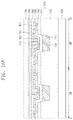
- FIGS. 11A to 23A and 11B to 23B illustrate cross-sectional views showing a method of fabricating a semiconductor light emitting device array according to some example embodiments.
- FIGS. 11A to 23A correspond to cross-sections taken along line D-D′ of FIG. 9
- FIGS. 11B to 23B correspond to cross-sections taken along line E-E′ of FIG. 9 .
- a growth substrate 100 may be provided.
- the growth substrate 100 may have a plurality of device regions DR.
- the term “device regions DR” may be areas on which semiconductor light emitting devices 10 are correspondingly formed.
- Each of the semiconductor light emitting devices 10 may be the semiconductor light emitting device 10 discussed with reference to FIGS. 1 to 6 .
- the plurality of device regions DR may be arranged two-dimensionally.
- a single semiconductor light emitting device 10 may be formed on one device region DR.
- a growth structure 110 a may be formed on the growth substrate 100 .
- the growth structure 110 a may include a first semiconductor layer 112 , an active layer 114 , and a second semiconductor layer 116 that are sequentially stacked on the growth substrate 100 .
- the first semiconductor layer 112 may be formed of n-type GaN
- the second semiconductor layer 116 may be formed of p-type GaN.
- the active layer 114 may be formed by alternately stacking multi-well layers of InGaN and quantum barrier layers of GaN.
- Each of the first semiconductor layer 112 , the active layer 114 , and the second semiconductor layer 116 may be formed by using metal organic chemical vapor deposition (MOCVD), hydride vapor phase epitaxy (HVPE), or molecular beam epitaxy (MBE).
- MOCVD metal organic chemical vapor deposition
- HVPE hydride vapor phase epitaxy
- MBE molecular beam epitaxy
- the growth structure 110 a may be partially etched to expose a portion of the first semiconductor layer 112 .
- the second semiconductor layer 116 , the active layer 114 , and the first semiconductor layer 112 may be partially and sequentially etched to form first openings OP 1 that expose the first semiconductor layer 112 .
- the first openings OP 1 may be formed on corresponding central portions of the device regions DR.
- a portion of each of the first openings OP 1 may have a shape that extends in one direction.
- each of the first openings OP 1 may have a first segment OP 1 a formed on the central portion of the device region DR and also have a second segment OP 1 b formed extending in one direction from the first segment OP 1 a .
- the second segment OP 1 b may pass through the first segment OP 1 a.
- first electrodes 120 may be formed in the first openings OP 1 .
- a photoresist PR may be formed on the second semiconductor layer 116 , exposing the first openings OP 1 .
- a conductive material may be deposited to fill the first openings OP 1 and to cover the photoresist PR.
- a lift-off process may be executed to remove the conductive material on the photoresist PR, or an etch-back process may be performed on the conductive material. After the etch-back process, portions of the conductive material may remain in the first openings OP 1 .
- First electrodes 120 may be defined to refer to the remaining portions of the conductive material in the first openings OP 1 .
- the etch-back process may continue until the first electrodes 120 have their top surfaces lower than a bottom surface of the active layer 114 .
- the first electrodes 120 may have portions, defined as extension portions 124 , that fill second segments OP 1 b of the first openings OP 1 , and the extension portions 124 may extend in one direction from corresponding first electrode 120 .
- recesses RS may be formed before the formation of the first openings OP 1 .
- a portion of the growth structure 110 a may be etched to partially expose the first semiconductor layer 112 .
- the second semiconductor layer 116 , the active layer 114 , and the first semiconductor layer 112 may be partially and sequentially etched to form the recesses RS that expose the first semiconductor layer 112 .
- the recesses RS may be formed on corresponding central portions of the device regions DR.
- a second dielectric layer 132 may be formed on the growth structure 110 a .
- the second dielectric layer 132 may cover a top surface of the second semiconductor layer 116 , inner lateral surfaces of the recesses RS, and bottom surfaces of the recesses RS.
- the second dielectric layer 132 may cover an exposed lateral surface of the active layer 114 and of the second semiconductor layer 116 .
- the second dielectric layer 132 may prevent the active layer 114 and the second semiconductor layer 116 from contacting first electrodes which will be formed in the following subsequent process.
- an etching process may be performed in which the second dielectric layer 132 and the first semiconductor layer 112 are partially and sequentially etched to form first openings OP 1 that expose the first semiconductor layer 112 .
- the etching process may be performed on a bottom surface of the second dielectric layer 132 .
- the first openings OP 1 may be formed on corresponding bottom surfaces of the recesses RS.
- Each of the first openings OP 1 may have a first segment OP 1 a formed on the central portion of the device region DR, and may also have a second segment OP 1 b formed extending in one direction from the first segment OP 1 a .
- first openings OP 1 may be filled with a conductive material to form first electrodes 120 .
- a semiconductor light emitting device array discussed with reference to FIGS. 5 and 6 . The following will continue to explain the example shown in FIGS. 9, 10, 12A, and 12B .
- a first dielectric layer 130 may be formed on the growth structure 110 a .
- the first dielectric layer 130 may cover the top surfaces of the first electrodes 120 and the top surface of the second semiconductor layer 116 .
- the first dielectric layer 130 may conformally cover the top surface of the second semiconductor layer 116 and inner lateral surfaces of the first openings OP 1 .
- the first dielectric layer 130 may be formed by deposition, such as chemical vapor deposition (CVD) or physical vapor deposition (PVD).
- second openings OP 2 may be formed in the first dielectric layer 130 .
- the second openings OP 2 may penetrate the first dielectric layer 130 , thereby exposing the top surface of the second semiconductor layer 116 .
- second electrodes 140 may be formed to cover a top surface of the first dielectric layer 130 and to partially fill the second openings OP 2 .
- the second electrodes 140 may be in contact with the second semiconductor layer 116 .
- the second electrodes 140 may be formed by using on the growth substrate 100 a deposition process, such as physical vapor deposition (PVD), to from a reflective metal layer, and then patterning the reflective metal layer.
- the reflective metal layer may include, for example, silver (Ag) or aluminum (Al).
- Each of the second electrodes 140 may be formed on the central portion of the device region DR, and may overlap its underlying first electrode 120 .
- the second electrodes 140 may be formed to cover the first electrodes 120 .
- the second electrodes 140 may be formed so as to expose the first dielectric layer 130 on outer edges of the device regions DR, as illustrated in FIG. 16A . In other example embodiments, the second electrodes 140 may be formed to completely fill the second openings OP 2 .
- a third dielectric layer 150 may be formed on the first dielectric layer 130 .
- the third dielectric layer 150 may cover the first dielectric layer 130 and the second electrodes 140 .
- the third dielectric layer 150 may be formed by deposition, such as chemical vapor deposition (CVD) or physical vapor deposition (PVD).
- Connection terminals 160 may be formed in the third dielectric layer 150 .
- holes exposing the second electrodes 140 may be formed, and then the holes may be filled with a conductive material to form the connection terminals 160 .
- a wiring substrate 210 may be provided.
- the wiring substrate 210 may have connection patterns 220 and a substrate dielectric layer 230 that are formed on one surface thereof.
- the connection patterns 220 may be exposed on one surface of the substrate dielectric layer 230 .
- the wiring substrate 210 , the connection patterns 220 and the substrate dielectric layer 230 may be formed separately from the components of FIGS. 11A-17B .
- the wiring substrate 210 may be aligned with the growth structure 110 a .
- the wiring substrate 210 may be aligned to align the substrate dielectric layer 230 with the third dielectric layer 150 , and the connection patterns 220 with the connection terminals 160 .
- the wiring substrate 210 may be attached onto the growth structure 110 a .
- the connection patterns 220 of the wiring substrate 210 may be coupled to the connection terminals 160 .
- the connection patterns 220 of the wiring substrate 210 may be electrically connected through the connection terminals 160 to the second electrodes 140 .
- the second electrodes 140 of each of semiconductor light emitting devices 10 a , 10 b , 10 c , and 10 d may be coupled to a separate circuit line of the wiring substrate 210 .
- external signals applied through the second electrodes 140 may drive the semiconductor light emitting devices 10 a , 10 b , 10 c , and 10 d to operate independently of each other.
- the substrate dielectric layer 230 of the wiring substrate 210 may be in contact with the third dielectric layer 150 . In this case, the substrate dielectric layer 230 and the third dielectric layer 150 may be attached to each other.
- the growth structure 110 a may be turned upside down to place the growth substrate 100 upwardly above the wiring substrate 210 . Afterwards, the growth substrate 100 may be removed.
- the growth structure 110 a may be etched to form light emitting structures 110 .
- an etching process may be performed in which the first semiconductor layer 112 , the active layer 114 , and the second semiconductor layer 116 are sequentially etched to form a trench T.
- the etching process may cause each of the first semiconductor layer 112 , the active layer 114 , and the second semiconductor layer 116 to be separated into a plurality of pieces.
- the trench T may be formed on edges of the device regions DR. For example, when viewed in plan, the trench T may surround the central portions of the device regions DR.
- the light emitting structures 110 may be formed on corresponding central portions of the device regions DR, and the trench T may separate the light emitting structures 110 from each other.
- the trench T may expose the third dielectric layer 150 .
- the extension portion 124 of the first electrode 120 may not be etched during the etching process.
- the extension portion 124 of the first electrode 120 may thus have an exposed top surface. In other example embodiments, the extension portion 124 may be etched during the etching process, and may not be exposed to the trench T.
- the semiconductor light emitting devices 10 may be constituted or formed each of which includes the light emitting structure 110 , the first electrode 120 , the first dielectric layer 130 , and the second electrode 140 . As discussed above, the semiconductor light emitting devices 10 may be provided on corresponding device regions DR.
- a device isolation layer 162 may be formed on the light emitting structure 110 .
- the device isolation layer 162 may be formed by coating or depositing a dielectric material on a top surface of the first semiconductor layer 112 and inner lateral and bottom surfaces of the trench T.
- Fifth openings OP 5 and sixth openings OP 6 may be formed in the device isolation layer 162 .
- the fifth openings OP 5 may be formed on corresponding central portions of the device regions DR, thereby exposing the top surfaces of the first semiconductor layers 112 .
- the sixth openings OP 6 may be formed on corresponding edges of the device regions DR, thereby exposing the top surfaces of the extension portions 124 included in the first electrodes 120 .
- a vertical conductive pattern 164 may be formed on the light emitting structures 110 .
- a conductive layer may be formed on the light emitting structures 110 .
- the conductive layer may cover the first semiconductor layers 112 and the device isolation layer 162 .
- the conductive layer may pass through the fifth openings OP 5 of the device isolation layer 162 and may contact the top surfaces of the first semiconductor layers 112 , and may pass through the sixth openings OP 6 of the device isolation layer 162 and may contact the extension portion 124 of the first electrode 120 .
- an etching process may be performed in which the conductive layer is etched to form the vertical conductive pattern 164 illustrated in FIGS. 22A and 22B .
- the etching process may form pixel openings POP that vertically penetrate the vertical conductive pattern 164 and expose the top surfaces of the first semiconductor layers 112 .
- FIGS. 22A and 22B show that the conductive layer is formed on the light emitting structures 110 and then is patterned to form the vertical conductive pattern 164 , but example embodiments are not limited thereto.
- sacrificial patterns may be formed on areas where the pixel openings POP will be formed, and thereafter spaces between the light emitting structures 110 and between the sacrificial patterns may be filled with a conductive material to form the vertical conductive pattern 164 .
- the filling of the conductive material may be performed by using a plating process or a deposition process.
- the vertical conductive pattern 164 may serve as a partition wall to prevent mutual interference of light generated from the light emitting structures 110 of the device regions DR. Accordingly, the light emitting structures 110 may independently constitute pixels that generate light different from each other. For example, a single pixel may be provided on one device region DR.
- the vertical conductive pattern 164 may be electrically connected to the extension portion 124 of the first electrode 120 included in each of the light emitting structures 110 .
- the vertical conductive pattern 164 may be coupled to all of the first electrodes 120 of the semiconductor light emitting devices 10 , and as shown in FIG. 10 , may serve as a common electrode of the semiconductor light emitting devices 10 .
- the vertical conductive pattern 164 may be provided in plural, and the plurality of vertical conductive patterns 164 may surround corresponding semiconductor light emitting devices 10 and may be insulated from each other.
- each of the vertical conductive patterns 164 may be a separate electrode of the semiconductor light emitting devices 10 corresponding thereto.
- the light emitting structure 110 may be coupled to an external circuit through the first electrode 120 and the vertical conductive pattern 164 .
- wavelength conversion layers CF may be formed in the pixel openings POP.
- a dispensing process may be performed in which the pixel openings POP are provided therein with a fluorescent material to form the wavelength conversion layers CF.
- the wavelength conversion layers CF may convert light emitted from corresponding semiconductor light emitting devices 10 into desired wavelengths.
- the wavelength conversion layers CF may include a wavelength conversion material.
- the wavelength conversion material may convert light having a wavelength generated from the semiconductor light emitting device 10 .
- the wavelength conversion material may include a quantum-dot fluorescent material, which has a nano-sized particle.
- the quantum-dot fluorescent material may use a III-V or II-VI compound semiconductor to have a core-shell structure.
- the core may include CdSe and/or InP.
- the shell may include ZnS and/or ZnSe.
- the quantum-dot fluorescent material may include a ligand to increase stability of the core and the shell.
- additional wavelength conversion particles may further be provided on an upper portion of one or more of the wavelength conversion layers CF.
- the wavelength conversion layers CF may include different fluorescent materials from each other on the device regions DR.
- one of the wavelength conversion layers CF may include one of red, green, and blue fluorescent materials, and a neighboring one of the wavelength conversion layers CF may include another of red, green, and blue fluorescent materials.
- a single pixel may be constituted by four semiconductor light emitting devices 10 a , 10 b , 10 c , and 10 d that are arranged adjacent to each other. For example, as illustrated in section A of FIG.
- four semiconductor light emitting devices 10 may be provided which are arranged adjacent to each other in row and column directions in a grid shape, and light from one of the semiconductor light emitting devices 10 a , 10 b , 10 c , and 10 d may be converted by its corresponding wavelength conversion layer CF into a desired wavelength different from that of light from another of the semiconductor light emitting devices 10 a , 10 b , 10 c , and 10 d .
- the wavelength conversion layer CF that corresponds to a first semiconductor light emitting device 10 a may convert an emitted light into a red light
- the wavelength conversion layers CF that correspond to second and third semiconductor light emitting devices 10 b and 10 c may covert an emitted light into a green light
- the wavelength conversion layer CF that corresponds to a fourth semiconductor light emitting device 10 d may convert an emitted light into a blue light.
- four semiconductor light emitting devices 10 a , 10 b , 10 c , and 10 d may constitute a single RGB pixel.
- light emitted from three ones 10 a , 10 b , and 10 d of four semiconductor light emitting devices 10 a , 10 b , 10 c , and 10 d may be converted into a red light, a green light, and a blue light, and the third semiconductor light emitting device 10 c may emit a white light without conversion.
- the third semiconductor light emitting device 10 c may omit the wavelength conversion layer CF, and instead include a transparent material layer.
- the third semiconductor light emitting device 10 c that emits a white light may control brightness of a single pixel.
- the first electrodes 120 of four semiconductor light emitting devices 10 a , 10 b , 10 c , and 10 d may be coupled to the vertical conductive pattern 164 serving as a common electrode, and each of the second electrodes 140 of four semiconductor light emitting devices 10 a , 10 b , 10 c , and 10 d may be coupled to a separate circuit line of the wiring substrate 210 .
- external signals applied through the second electrodes 140 may drive the first to fourth semiconductor light emitting devices 10 a , 10 b , 10 c , and 10 d to operate independently of each other.
- FIGS. 23A and 23B show that the wavelength conversion layers CF have their flat top surfaces, but each of the wavelength conversion layers CF may have, on a central portion thereof, a top surface at a higher level than that of a top surface on other portion thereof.
- a single pixel is constituted by four semiconductor light emitting devices 10 a , 10 b , 10 c , and 10 d that are arranged in a grid shape, but example embodiments are not limited thereto.
- a single pixel may be constituted by three semiconductor light emitting devices 10 e , 10 f , and 10 g that are arranged in one direction parallel to the growth substrate 100 .
- the wavelength conversion layer CF that corresponds to a fifth semiconductor light emitting device 10 e may convert an emitted light into a red light
- the wavelength conversion layers CF that corresponds to a sixth semiconductor light emitting devices 10 f may covert an emitted light into a green light
- the wavelength conversion layer CF that corresponds to a seventh semiconductor light emitting device 10 g may convert an emitted light into a blue light.
- three semiconductor light emitting devices 10 e , 10 f , and 10 g may constitute a single RGB pixel
- the first electrodes 120 of three semiconductor light emitting devices 10 e , 10 f , and 10 g may be coupled to the vertical conductive pattern 164 serving as a common electrode
- each of the second electrodes 140 of three semiconductor light emitting devices 10 e , 10 f , and 10 g may be coupled to a separate circuit line of the wiring substrate 210 .
- three semiconductor light emitting devices 10 e , 10 f , and 10 g may independently operate to produce a single color.
- a semiconductor light emitting device array may include a plurality of semiconductor light emitting devices.
- the vertical conductive pattern 164 may be provided between the plurality of semiconductor light emitting devices.
- the vertical conductive pattern 164 may divide the semiconductor light emitting devices from each other, and may be coupled to the extension portion 124 of the first electrode 120 of each semiconductor light emitting device to thereby apply an electrical signal to the first electrode 120 .
- the device isolation layer 162 may be interposed between the vertical conductive pattern 164 and an outer lateral surface of the semiconductor light emitting device (or, a lateral surface of the first semiconductor layer 112 , of the active layer, and of the second semiconductor layer 116 ), and may prevent the vertical conductive pattern 164 from being in contact with the first semiconductor layer 112 , the active layer 114 , and the second semiconductor layer 116 .
- a semiconductor light emitting device array may be fabricated which includes the semiconductor light emitting device 10 of FIG. 2A .
- FIG. 24 illustrates a plan view showing a method of fabricating a semiconductor light emitting device array according to some example embodiments.
- FIGS. 25 and 26 illustrate cross-sectional views taken along line F-F′ of FIG. 23 , showing a method of fabricating a semiconductor light emitting device array according to some example embodiments.
- the growth structure 110 a may be formed on the growth substrate 100 .
- the first openings OP 1 may be formed on the growth structure 110 a .
- the first openings OP 1 may be formed to have only first segments OP 1 a formed on corresponding central portions of the device regions DR. Therefore, the first electrodes 120 may not have the extension portions 124 .
- the first dielectric layer 130 and the second electrodes 140 may be formed on the first electrodes 120 .
- the growth substrate 100 may be removed to expose a bottom surface of the first semiconductor layer 112 .
- a grinding process may be performed on the exposed bottom surface of the first semiconductor layer 112 .
- the grinding process may continue until bottom surfaces of the first electrodes 120 are exposed.
- a wiring process may be performed on the bottom surface of the first semiconductor layer 112 .
- the growth substrate 100 may be removed to expose the bottom surface of the first semiconductor layer 112 .
- An etching process may be performed on the exposed bottom surface of the first semiconductor layer 112 , thereby forming fourth openings OP 4 .
- the fourth openings OP 4 may expose the bottom surfaces of the first electrodes 120 .
- the fourth openings OP 4 may be filled with a conductive material to form sub-electrodes 122 .
- the sub-electrodes 122 may be coupled to the first electrodes 120 .
- a wiring process may be performed on the bottom surface of the first semiconductor layer 112 .
- a semiconductor light emitting device may include a first electrode and a second electrode which are used to apply electrical signals to a light emitting structure, where the first and second electrodes vertically overlap each other. Accordingly, the first and second electrodes may be placed in a small area, and as a result the semiconductor light emitting device may be easily reduced in size.
- the first electrode may be buried in a first opening of the light emitting structure, and may be in contact with top and inner lateral surfaces of a first semiconductor layer exposed to the first opening. Accordingly, an n-contact between the first electrode and the first semiconductor layer may have a large area, and electrical characteristics of the semiconductor light emitting device may be improved.
Landscapes
- Led Devices (AREA)
Abstract
Description
Claims (19)
Applications Claiming Priority (2)
| Application Number | Priority Date | Filing Date | Title |
|---|---|---|---|
| KR1020190150455A KR102740584B1 (en) | 2019-11-21 | 2019-11-21 | Semiconductor light emitting device and a method for manufacturing the same |
| KR10-2019-0150455 | 2019-11-21 |
Publications (2)
| Publication Number | Publication Date |
|---|---|
| US20210159365A1 US20210159365A1 (en) | 2021-05-27 |
| US11515449B2 true US11515449B2 (en) | 2022-11-29 |
Family
ID=75974528
Family Applications (1)
| Application Number | Title | Priority Date | Filing Date |
|---|---|---|---|
| US16/935,356 Active 2040-08-03 US11515449B2 (en) | 2019-11-21 | 2020-07-22 | Semiconductor light emitting device and method of fabricating the same |
Country Status (2)
| Country | Link |
|---|---|
| US (1) | US11515449B2 (en) |
| KR (1) | KR102740584B1 (en) |
Citations (15)
| Publication number | Priority date | Publication date | Assignee | Title |
|---|---|---|---|---|
| US8471288B2 (en) | 2009-09-15 | 2013-06-25 | Toyoda Gosei Co., Ltd. | Group III nitride semiconductor light-emitting device including an auxiliary electrode in contact with a back surface of an n-type layer |
| US8502193B2 (en) | 2008-04-16 | 2013-08-06 | Lg Innotek Co., Ltd. | Light-emitting device and fabricating method thereof |
| KR20150089769A (en) | 2014-01-28 | 2015-08-05 | 엘지이노텍 주식회사 | Light emitting device |
| US9293664B2 (en) | 2010-09-24 | 2016-03-22 | Seoul Semiconductor Co., Ltd. | Wafer-level light emitting diode package and method of fabricating the same |
| US9299742B2 (en) | 2011-08-15 | 2016-03-29 | Micron Technology, Inc. | High-voltage solid-state transducers and associated systems and methods |
| US20160268478A1 (en) * | 2015-03-12 | 2016-09-15 | Kabushiki Kaisha Toshiba | Semiconductor light-emitting device |
| US20160276539A1 (en) * | 2015-03-16 | 2016-09-22 | Kabushiki Kaisha Toshiba | Semiconductor light-emitting element |
| US20160351751A1 (en) * | 2015-05-25 | 2016-12-01 | Lextar Electronics Corporation | Semiconductor light emitting structure and manufacturing method thereof |
| US20170040515A1 (en) * | 2015-08-06 | 2017-02-09 | Samsung Electronics Co., Ltd. | Semiconductor light emitting device and method of manufacturing the same |
| US9680063B2 (en) | 2015-05-14 | 2017-06-13 | Stanley Electric Co., Ltd. | Semiconductor light-emitting device and semiconductor light-emitting device array |
| KR101773582B1 (en) | 2010-12-28 | 2017-08-31 | 서울바이오시스 주식회사 | High efficiency light emitting diode |
| KR101780893B1 (en) | 2016-03-10 | 2017-09-22 | 희성전자 주식회사 | Electro luminescence device included in lighting apparatus and method of manufacturing the same |
| US20180047780A1 (en) * | 2016-08-11 | 2018-02-15 | Samsung Electronics Co., Ltd. | Light emitting device package and display device using the same |
| KR101861632B1 (en) | 2011-06-02 | 2018-05-28 | 엘지이노텍 주식회사 | A light emitting device and a light emitting device package |
| US20200020739A1 (en) * | 2018-07-12 | 2020-01-16 | Epistar Corporation | Light-emitting device |
Family Cites Families (2)
| Publication number | Priority date | Publication date | Assignee | Title |
|---|---|---|---|---|
| KR101252032B1 (en) * | 2010-07-08 | 2013-04-10 | 삼성전자주식회사 | Semiconductor light emitting device and method of manufacturing the same |
| KR20160141301A (en) * | 2015-05-29 | 2016-12-08 | 삼성전자주식회사 | Semiconductor light emitting device package |
-
2019
- 2019-11-21 KR KR1020190150455A patent/KR102740584B1/en active Active
-
2020
- 2020-07-22 US US16/935,356 patent/US11515449B2/en active Active
Patent Citations (15)
| Publication number | Priority date | Publication date | Assignee | Title |
|---|---|---|---|---|
| US8502193B2 (en) | 2008-04-16 | 2013-08-06 | Lg Innotek Co., Ltd. | Light-emitting device and fabricating method thereof |
| US8471288B2 (en) | 2009-09-15 | 2013-06-25 | Toyoda Gosei Co., Ltd. | Group III nitride semiconductor light-emitting device including an auxiliary electrode in contact with a back surface of an n-type layer |
| US9293664B2 (en) | 2010-09-24 | 2016-03-22 | Seoul Semiconductor Co., Ltd. | Wafer-level light emitting diode package and method of fabricating the same |
| KR101773582B1 (en) | 2010-12-28 | 2017-08-31 | 서울바이오시스 주식회사 | High efficiency light emitting diode |
| KR101861632B1 (en) | 2011-06-02 | 2018-05-28 | 엘지이노텍 주식회사 | A light emitting device and a light emitting device package |
| US9299742B2 (en) | 2011-08-15 | 2016-03-29 | Micron Technology, Inc. | High-voltage solid-state transducers and associated systems and methods |
| KR20150089769A (en) | 2014-01-28 | 2015-08-05 | 엘지이노텍 주식회사 | Light emitting device |
| US20160268478A1 (en) * | 2015-03-12 | 2016-09-15 | Kabushiki Kaisha Toshiba | Semiconductor light-emitting device |
| US20160276539A1 (en) * | 2015-03-16 | 2016-09-22 | Kabushiki Kaisha Toshiba | Semiconductor light-emitting element |
| US9680063B2 (en) | 2015-05-14 | 2017-06-13 | Stanley Electric Co., Ltd. | Semiconductor light-emitting device and semiconductor light-emitting device array |
| US20160351751A1 (en) * | 2015-05-25 | 2016-12-01 | Lextar Electronics Corporation | Semiconductor light emitting structure and manufacturing method thereof |
| US20170040515A1 (en) * | 2015-08-06 | 2017-02-09 | Samsung Electronics Co., Ltd. | Semiconductor light emitting device and method of manufacturing the same |
| KR101780893B1 (en) | 2016-03-10 | 2017-09-22 | 희성전자 주식회사 | Electro luminescence device included in lighting apparatus and method of manufacturing the same |
| US20180047780A1 (en) * | 2016-08-11 | 2018-02-15 | Samsung Electronics Co., Ltd. | Light emitting device package and display device using the same |
| US20200020739A1 (en) * | 2018-07-12 | 2020-01-16 | Epistar Corporation | Light-emitting device |
Also Published As
| Publication number | Publication date |
|---|---|
| KR20210062777A (en) | 2021-06-01 |
| US20210159365A1 (en) | 2021-05-27 |
| KR102740584B1 (en) | 2024-12-12 |
Similar Documents
| Publication | Publication Date | Title |
|---|---|---|
| US11329207B2 (en) | Emissive display device comprising LEDs | |
| US11251167B2 (en) | Multi-junction LED with eutectic bonding and method of manufacturing the same | |
| US10403608B2 (en) | Light-emitting diode (LED) device for realizing multi-colors | |
| US12176379B2 (en) | Optoelectronic device comprising pixels which emit three colors | |
| US11742469B2 (en) | Semiconductor light-emitting device and method of fabricating the same | |
| US10573786B2 (en) | Semiconductor light emitting device | |
| KR102462658B1 (en) | Light emitting device and display device having thereof | |
| KR20180055971A (en) | Semiconductor light emitting device having a reflector layer of multilayer structure | |
| CN109273572B (en) | Semiconductor light emitting device | |
| US20210351229A1 (en) | Light emitting device for display and display apparatus having the same | |
| KR20170133758A (en) | Light emitting device | |
| KR20170133746A (en) | Light emitting device | |
| KR102566499B1 (en) | Light emitting device | |
| US20130221398A1 (en) | Semiconductor light emitting device and fabrication method thereof | |
| CN113261117A (en) | Light emitting element | |
| TWI799765B (en) | Light emitting diode precursor | |
| US11735694B2 (en) | Semiconductor light emitting device and semiconductor light emitting package | |
| US11515449B2 (en) | Semiconductor light emitting device and method of fabricating the same | |
| US11380818B2 (en) | Semiconductor light emitting device | |
| KR102736947B1 (en) | Light-emitting element | |
| KR102489464B1 (en) | Light emitting device and method of fabricating the same | |
| US12484362B2 (en) | Display device | |
| KR20110085727A (en) | Semiconductor light emitting device and method for manufacturing same |
Legal Events
| Date | Code | Title | Description |
|---|---|---|---|
| AS | Assignment |
Owner name: SAMSUNG ELECTRONICS CO., LTD., KOREA, REPUBLIC OF Free format text: ASSIGNMENT OF ASSIGNORS INTEREST;ASSIGNORS:YANG, JONGIN;KIM, YONGIL;KIM, JUHYUN;AND OTHERS;SIGNING DATES FROM 20200518 TO 20200617;REEL/FRAME:053277/0692 |
|
| FEPP | Fee payment procedure |
Free format text: ENTITY STATUS SET TO UNDISCOUNTED (ORIGINAL EVENT CODE: BIG.); ENTITY STATUS OF PATENT OWNER: LARGE ENTITY |
|
| STPP | Information on status: patent application and granting procedure in general |
Free format text: DOCKETED NEW CASE - READY FOR EXAMINATION |
|
| STPP | Information on status: patent application and granting procedure in general |
Free format text: NON FINAL ACTION MAILED |
|
| STPP | Information on status: patent application and granting procedure in general |
Free format text: RESPONSE TO NON-FINAL OFFICE ACTION ENTERED AND FORWARDED TO EXAMINER |
|
| STPP | Information on status: patent application and granting procedure in general |
Free format text: FINAL REJECTION MAILED |
|
| STPP | Information on status: patent application and granting procedure in general |
Free format text: RESPONSE AFTER FINAL ACTION FORWARDED TO EXAMINER |
|
| STPP | Information on status: patent application and granting procedure in general |
Free format text: NOTICE OF ALLOWANCE MAILED -- APPLICATION RECEIVED IN OFFICE OF PUBLICATIONS |
|
| STPP | Information on status: patent application and granting procedure in general |
Free format text: PUBLICATIONS -- ISSUE FEE PAYMENT VERIFIED |
|
| STCF | Information on status: patent grant |
Free format text: PATENTED CASE |