US11511519B2 - Titanium part having an etched surface - Google Patents
Titanium part having an etched surface Download PDFInfo
- Publication number
- US11511519B2 US11511519B2 US16/867,200 US202016867200A US11511519B2 US 11511519 B2 US11511519 B2 US 11511519B2 US 202016867200 A US202016867200 A US 202016867200A US 11511519 B2 US11511519 B2 US 11511519B2
- Authority
- US
- United States
- Prior art keywords
- channel
- titanium alloy
- metal
- channels
- opening
- Prior art date
- Legal status (The legal status is an assumption and is not a legal conclusion. Google has not performed a legal analysis and makes no representation as to the accuracy of the status listed.)
- Active, expires
Links
- RTAQQCXQSZGOHL-UHFFFAOYSA-N Titanium Chemical group [Ti] RTAQQCXQSZGOHL-UHFFFAOYSA-N 0.000 title description 59
- 239000000758 substrate Substances 0.000 claims abstract description 107
- 229910001069 Ti alloy Inorganic materials 0.000 claims abstract description 37
- 229910052751 metal Inorganic materials 0.000 claims description 112
- 239000002184 metal Substances 0.000 claims description 112
- 238000000034 method Methods 0.000 claims description 102
- 230000008569 process Effects 0.000 claims description 76
- 238000005530 etching Methods 0.000 claims description 72
- 229910052755 nonmetal Inorganic materials 0.000 claims description 47
- 239000000463 material Substances 0.000 claims description 4
- VEXZGXHMUGYJMC-UHFFFAOYSA-M Chloride anion Chemical compound [Cl-] VEXZGXHMUGYJMC-UHFFFAOYSA-M 0.000 claims description 2
- 229910052719 titanium Inorganic materials 0.000 description 49
- 239000010936 titanium Substances 0.000 description 49
- 229910044991 metal oxide Inorganic materials 0.000 description 26
- 150000004706 metal oxides Chemical class 0.000 description 26
- 239000002861 polymer material Substances 0.000 description 18
- 239000011148 porous material Substances 0.000 description 15
- 239000000243 solution Substances 0.000 description 15
- 238000004140 cleaning Methods 0.000 description 10
- 229920000642 polymer Polymers 0.000 description 10
- 238000007743 anodising Methods 0.000 description 9
- FAPWRFPIFSIZLT-UHFFFAOYSA-M Sodium chloride Chemical compound [Na+].[Cl-] FAPWRFPIFSIZLT-UHFFFAOYSA-M 0.000 description 8
- 238000007254 oxidation reaction Methods 0.000 description 8
- QAOWNCQODCNURD-UHFFFAOYSA-N Sulfuric acid Chemical compound OS(O)(=O)=O QAOWNCQODCNURD-UHFFFAOYSA-N 0.000 description 7
- 230000002378 acidificating effect Effects 0.000 description 7
- 229910052782 aluminium Inorganic materials 0.000 description 7
- VEXZGXHMUGYJMC-UHFFFAOYSA-N Hydrochloric acid Chemical compound Cl VEXZGXHMUGYJMC-UHFFFAOYSA-N 0.000 description 6
- NBIIXXVUZAFLBC-UHFFFAOYSA-N Phosphoric acid Chemical compound OP(O)(O)=O NBIIXXVUZAFLBC-UHFFFAOYSA-N 0.000 description 6
- XAGFODPZIPBFFR-UHFFFAOYSA-N aluminium Chemical compound [Al] XAGFODPZIPBFFR-UHFFFAOYSA-N 0.000 description 6
- 230000015572 biosynthetic process Effects 0.000 description 6
- 150000004820 halides Chemical class 0.000 description 6
- 239000007769 metal material Substances 0.000 description 6
- 230000003647 oxidation Effects 0.000 description 6
- 229910045601 alloy Inorganic materials 0.000 description 5
- 239000000956 alloy Substances 0.000 description 5
- 238000007796 conventional method Methods 0.000 description 5
- 239000011521 glass Substances 0.000 description 4
- 238000003754 machining Methods 0.000 description 4
- 229910052760 oxygen Inorganic materials 0.000 description 4
- 230000035515 penetration Effects 0.000 description 4
- 238000007788 roughening Methods 0.000 description 4
- 239000011780 sodium chloride Substances 0.000 description 4
- OKTJSMMVPCPJKN-UHFFFAOYSA-N Carbon Chemical compound [C] OKTJSMMVPCPJKN-UHFFFAOYSA-N 0.000 description 3
- 241000237503 Pectinidae Species 0.000 description 3
- 229910000147 aluminium phosphate Inorganic materials 0.000 description 3
- QVGXLLKOCUKJST-UHFFFAOYSA-N atomic oxygen Chemical compound [O] QVGXLLKOCUKJST-UHFFFAOYSA-N 0.000 description 3
- 229910052799 carbon Inorganic materials 0.000 description 3
- 238000001746 injection moulding Methods 0.000 description 3
- 239000007788 liquid Substances 0.000 description 3
- 150000002739 metals Chemical class 0.000 description 3
- 238000001000 micrograph Methods 0.000 description 3
- 239000001301 oxygen Substances 0.000 description 3
- 235000020637 scallop Nutrition 0.000 description 3
- XLYOFNOQVPJJNP-UHFFFAOYSA-N water Substances O XLYOFNOQVPJJNP-UHFFFAOYSA-N 0.000 description 3
- CPELXLSAUQHCOX-UHFFFAOYSA-M Bromide Chemical compound [Br-] CPELXLSAUQHCOX-UHFFFAOYSA-M 0.000 description 2
- GRYLNZFGIOXLOG-UHFFFAOYSA-N Nitric acid Chemical compound O[N+]([O-])=O GRYLNZFGIOXLOG-UHFFFAOYSA-N 0.000 description 2
- 239000004696 Poly ether ether ketone Substances 0.000 description 2
- 229910000883 Ti6Al4V Inorganic materials 0.000 description 2
- GWEVSGVZZGPLCZ-UHFFFAOYSA-N Titan oxide Chemical compound O=[Ti]=O GWEVSGVZZGPLCZ-UHFFFAOYSA-N 0.000 description 2
- 239000000853 adhesive Substances 0.000 description 2
- 230000001070 adhesive effect Effects 0.000 description 2
- 230000008901 benefit Effects 0.000 description 2
- 238000013500 data storage Methods 0.000 description 2
- 230000006870 function Effects 0.000 description 2
- 230000001788 irregular Effects 0.000 description 2
- 229910001092 metal group alloy Inorganic materials 0.000 description 2
- 229910017604 nitric acid Inorganic materials 0.000 description 2
- 229920006260 polyaryletherketone Polymers 0.000 description 2
- 229920002530 polyetherether ketone Polymers 0.000 description 2
- 229920000139 polyethylene terephthalate Polymers 0.000 description 2
- 239000005020 polyethylene terephthalate Substances 0.000 description 2
- 239000011253 protective coating Substances 0.000 description 2
- 238000007789 sealing Methods 0.000 description 2
- 230000002269 spontaneous effect Effects 0.000 description 2
- 239000010935 stainless steel Substances 0.000 description 2
- 229910001220 stainless steel Inorganic materials 0.000 description 2
- 239000000126 substance Substances 0.000 description 2
- -1 titanium ions Chemical class 0.000 description 2
- OGIDPMRJRNCKJF-UHFFFAOYSA-N titanium oxide Inorganic materials [Ti]=O OGIDPMRJRNCKJF-UHFFFAOYSA-N 0.000 description 2
- 229910000838 Al alloy Inorganic materials 0.000 description 1
- XOJVVFBFDXDTEG-UHFFFAOYSA-N Norphytane Natural products CC(C)CCCC(C)CCCC(C)CCCC(C)C XOJVVFBFDXDTEG-UHFFFAOYSA-N 0.000 description 1
- 229910000831 Steel Inorganic materials 0.000 description 1
- 239000010407 anodic oxide Substances 0.000 description 1
- 238000002048 anodisation reaction Methods 0.000 description 1
- 230000000712 assembly Effects 0.000 description 1
- 238000000429 assembly Methods 0.000 description 1
- JUPQTSLXMOCDHR-UHFFFAOYSA-N benzene-1,4-diol;bis(4-fluorophenyl)methanone Chemical compound OC1=CC=C(O)C=C1.C1=CC(F)=CC=C1C(=O)C1=CC=C(F)C=C1 JUPQTSLXMOCDHR-UHFFFAOYSA-N 0.000 description 1
- 238000005422 blasting Methods 0.000 description 1
- 239000000919 ceramic Substances 0.000 description 1
- 239000011248 coating agent Substances 0.000 description 1
- 238000000576 coating method Methods 0.000 description 1
- 239000000356 contaminant Substances 0.000 description 1
- 238000005260 corrosion Methods 0.000 description 1
- 230000007797 corrosion Effects 0.000 description 1
- 238000005238 degreasing Methods 0.000 description 1
- 239000003989 dielectric material Substances 0.000 description 1
- 230000009977 dual effect Effects 0.000 description 1
- 238000001978 electrochemical passivation Methods 0.000 description 1
- 229910002804 graphite Inorganic materials 0.000 description 1
- 239000010439 graphite Substances 0.000 description 1
- 238000007654 immersion Methods 0.000 description 1
- 230000014759 maintenance of location Effects 0.000 description 1
- 238000013507 mapping Methods 0.000 description 1
- 238000012986 modification Methods 0.000 description 1
- 230000004048 modification Effects 0.000 description 1
- 239000002071 nanotube Substances 0.000 description 1
- 229910052757 nitrogen Inorganic materials 0.000 description 1
- 239000003921 oil Substances 0.000 description 1
- 230000003287 optical effect Effects 0.000 description 1
- 239000002245 particle Substances 0.000 description 1
- 238000002161 passivation Methods 0.000 description 1
- 239000000049 pigment Substances 0.000 description 1
- 238000007517 polishing process Methods 0.000 description 1
- 238000012545 processing Methods 0.000 description 1
- 230000009257 reactivity Effects 0.000 description 1
- 230000000717 retained effect Effects 0.000 description 1
- 239000007787 solid Substances 0.000 description 1
- 239000010959 steel Substances 0.000 description 1
- 238000004381 surface treatment Methods 0.000 description 1
- 238000012360 testing method Methods 0.000 description 1
- 229920001169 thermoplastic Polymers 0.000 description 1
- 239000004416 thermosoftening plastic Substances 0.000 description 1
Images


Classifications
-
- C—CHEMISTRY; METALLURGY
- C25—ELECTROLYTIC OR ELECTROPHORETIC PROCESSES; APPARATUS THEREFOR
- C25F—PROCESSES FOR THE ELECTROLYTIC REMOVAL OF MATERIALS FROM OBJECTS; APPARATUS THEREFOR
- C25F3/00—Electrolytic etching or polishing
- C25F3/02—Etching
- C25F3/04—Etching of light metals
-
- B—PERFORMING OPERATIONS; TRANSPORTING
- B32—LAYERED PRODUCTS
- B32B—LAYERED PRODUCTS, i.e. PRODUCTS BUILT-UP OF STRATA OF FLAT OR NON-FLAT, e.g. CELLULAR OR HONEYCOMB, FORM
- B32B15/00—Layered products comprising a layer of metal
- B32B15/04—Layered products comprising a layer of metal comprising metal as the main or only constituent of a layer, which is next to another layer of the same or of a different material
- B32B15/08—Layered products comprising a layer of metal comprising metal as the main or only constituent of a layer, which is next to another layer of the same or of a different material of synthetic resin
-
- B—PERFORMING OPERATIONS; TRANSPORTING
- B32—LAYERED PRODUCTS
- B32B—LAYERED PRODUCTS, i.e. PRODUCTS BUILT-UP OF STRATA OF FLAT OR NON-FLAT, e.g. CELLULAR OR HONEYCOMB, FORM
- B32B3/00—Layered products comprising a layer with external or internal discontinuities or unevennesses, or a layer of non-planar shape; Layered products comprising a layer having particular features of form
- B32B3/26—Layered products comprising a layer with external or internal discontinuities or unevennesses, or a layer of non-planar shape; Layered products comprising a layer having particular features of form characterised by a particular shape of the outline of the cross-section of a continuous layer; characterised by a layer with cavities or internal voids ; characterised by an apertured layer
- B32B3/30—Layered products comprising a layer with external or internal discontinuities or unevennesses, or a layer of non-planar shape; Layered products comprising a layer having particular features of form characterised by a particular shape of the outline of the cross-section of a continuous layer; characterised by a layer with cavities or internal voids ; characterised by an apertured layer characterised by a layer formed with recesses or projections, e.g. hollows, grooves, protuberances, ribs
-
- C—CHEMISTRY; METALLURGY
- C22—METALLURGY; FERROUS OR NON-FERROUS ALLOYS; TREATMENT OF ALLOYS OR NON-FERROUS METALS
- C22C—ALLOYS
- C22C14/00—Alloys based on titanium
Definitions
- the described embodiments relate generally to etching a surface of a titanium part. More particularly, the described embodiments relate to techniques for forming an interconnected network of channels throughout the titanium part by using an electrochemical etching process.
- Enclosures for portable electronic devices may be formed from a combination of metal and non-metal materials.
- metal lacks a natural ability to attach to these non-metal materials.
- conventional techniques for modifying metal parts, in an attempt to provide a strong attachment between these metal parts and non-metal parts have proved unsuccessful.
- surfaces of these metal parts may be superficially roughened. However, this superficial roughness is hardly sufficient to provide the ideal structure for bonding metal parts to non-metal parts.
- the described embodiments relate generally to etching a surface of a titanium part. More particularly, the described embodiments relate to techniques for forming an interconnected network of channels throughout the titanium part by using an electrochemical etching process.
- a titanium alloy substrate for a portable electronic device includes an exterior surface and a branching channel structure that includes a first channel and a second channel, where the first channel is defined by a first channel wall that extends away from a first opening in the exterior surface, and the second channel is defined by a second channel wall that extends away from a second opening in the first channel wall.
- an enclosure for a portable electronic device includes a first portion including a metal substrate, the metal substrate including an interconnected network of channels.
- the channels include a first channel defined by a first channel wall, where the first channel wall extends from a first opening in an external surface of the metal substrate and terminates at a first terminus surface within the metal substrate, and a second channel defined by a second channel wall, where the second channel wall extends between a second opening in the external surface of the metal substrate and a third opening in the first channel wall.
- the enclosure further includes a second portion including protruding features that extend through the first and second openings and into the first and second channels.
- a method for forming a part for a portable electronic device the part including a titanium alloy substrate, is described.
- the method includes exposing an exterior surface of the titanium alloy substrate to an electrochemical etching process, where the electrochemical etching process forms (i) an opening in the exterior surface and a first channel defined by a first channel wall that extends from the opening, and (ii) an opening in the first channel wall and a second channel defined by a second channel wall that extends from the opening in the first channel wall.
- FIG. 1 illustrates perspective views of various portable electronic devices having enclosures that may be processed using the techniques described herein, in accordance with some embodiments.
- FIGS. 2A-2I illustrate exemplary cross-sectional views of a process for forming an etched metal part, in accordance with some embodiments.
- FIGS. 3A-3B illustrate various views of an etched metal part, in accordance with some embodiments.
- FIGS. 4A-4B illustrate various views of an etched metal part that is locked to a non-metal part, in accordance with some embodiments.
- FIG. 5 illustrates a method for forming an etched part, in accordance with some embodiments.
- FIG. 6 illustrates an exemplary top-down image of an etched metal part, in accordance with some embodiments.
- FIG. 7 illustrates an exemplary, magnified, top-down image of an etched metal part, in accordance with some embodiments.
- FIG. 8 illustrates an exemplary cross-sectional image of an etched metal part, in accordance with some embodiments.
- Enclosures for portable electronic devices may be formed from a variety of different materials.
- the enclosure may be formed from titanium, which is attractive over stainless steel and aluminum due to titanium's high strength-to-weight ratio. Additionally, the enclosure may also be formed from a non-metal material, such as glass or a polymer.
- display assemblies of portable electronic devices may be bonded to a titanium frame of an enclosure.
- the titanium frame may be sub-divided into various electrically isolated parts such as to prevent electromagnetic interference of antenna(s) carried within the enclosure.
- titanium may be used to form a structural band around the edges of the enclosure such that the display is bonded to one face, and a glass is bound to the opposing face.
- a polymer material may be used to form electrical insulating splits that interlock the separate portions of the titanium frame together. The polymer material may be used as a dielectric material that prevents electromagnetic interference.
- the enclosure requires a strong adhesive bond to be formed between the metal (e.g., titanium) and the non-metal material (e.g., polymer).
- the metal e.g., titanium
- the non-metal material e.g., polymer
- these requirements are even more technically challenging to satisfy in the face of additional insulating splits (for improved antenna performance) and even smaller areas of adhesion (to minimize weight and space).
- the increasing need for water-resistant enclosures demands that these adhesive bonds must not only maintain strength, but also prevent moisture leakage—even after the enclosure has been subjected to many strain cycles.
- titanium and its alloys thereof are characterized as having a high specific strength and stiffness.
- titanium has a Vickers hardness number of ⁇ 350 HV1.
- titanium can function as a protective coating to protect internal operational components carried by the enclosures, for example, when these portable electronic devices are dropped, scratched, chipped, or abraded.
- this hardness it is also difficult to polish and/or machine the surface of the titanium substrate using conventional techniques. Indeed, the relative hardness of titanium relative to other metals allows for only a limited amount of roughening using conventional techniques. Titanium is also highly resistant to corrosion.
- the embodiments described herein set forth techniques for etching an external surface of a substrate that includes titanium such as to form an interconnected network of channels within the substrate.
- the techniques involve using an electrochemical etching process to etch a thin metal oxide layer that overlays the substrate.
- the electrochemical etching process is a controlled process for etching the substrate, such as by controlling parameters that include temperature, voltage, and concentration of the etchant solution. Controlling these parameters can be used to control the depth, diameter, and/or concentration of the pore structures formed within the substrate. It should be noted that the techniques in the embodiments described herein can prevent over-etching of the external surface of the substrate.
- Over-etching of the external surface may be undesirable in that it significantly reduces the number of pore structures within the substrate, thereby, reducing potential attachment strength between the metal part and the non-metal material relative to an external surface having a moderate amount of etching.
- over-etching of the external surface is characterized by multiple openings at the external surface that overlap one another at a single region.
- over-etching of the metal substrate can compromise the structural integrity and/or hardness of the metal substrate.
- anodic film, anodized film, anodic layer, anodized layer, anodic oxide coating, anodic layer, anodic oxidized layer, metal oxide layer, oxide film, oxidized layer, and oxide layer can be used interchangeably where appropriate.
- an anodized layer can result from an electrochemical anodization process of aluminum or an aluminum alloy.
- metal oxide layers can result from a non-electrolytic passivation process.
- the metal substrate can include any of a number of suitable metals or metal alloys thereof such as aluminum, titanium, steel, and the like. It should be noted that the processes for forming an anodized layer and a metal oxide layer may be different.
- the terms segment, region, and section can also be used interchangeably where appropriate.
- a titanium alloy substrate for a portable electronic device includes a titanium alloy substrate for a portable electronic device is described.
- the titanium alloy substrate includes an exterior surface and a branching channel structure that includes a first channel and a second channel, where the first channel is defined by a first channel wall that extends away from a first opening in the exterior surface, and the second channel is defined by a second channel wall that extends away from a second opening in the first channel wall.
- FIGS. 1-8 These and other embodiments are discussed below with reference to FIGS. 1-8 ; however, those skilled in the art will readily appreciate that the detailed description given herein with respect to these figures is for explanatory purposes only and should not be construed as limiting.
- FIG. 1 illustrates various portable electronic devices that can be processed using the techniques as described herein.
- the techniques as described herein can be used to process surfaces of enclosures of the portable electronic devices.
- the enclosures can include at least one of a metal, a metal alloy, a polymer, glass, ceramics, or a thermoplastic.
- the enclosures can include a metal part that is attached to a non-metal part.
- the non-metal part can include a polymer.
- the techniques described herein may be used to color the metal surfaces by causing color particles (e.g., water-soluble pigments, dye, etc.) to become absorbed within the metal surfaces.
- color particles e.g., water-soluble pigments, dye, etc.
- FIG. 1 illustrates exemplary portable electronic devices including a smartphone 102 , a tablet computer 104 , a smartwatch 106 , and a portable computer 108 that include enclosures that may be processed using the techniques as described herein.
- These exemplary portable electronic devices may be capable of using personally identifiable information that is associated with one or more users. It is well understood that the use of personally identifiable information should follow privacy policies and practices that are generally recognized as meeting or exceeding industry or governmental requirements for maintaining the privacy of users. In particular, personally identifiable information data should be managed and handled so as to minimize risks of unintentional or unauthorized access or use, and the nature of authorized use should be clearly indicated to users.
- the enclosures may have a three-dimensional structure having a height, width, and depth, and any type of geometry.
- the enclosures is characterized as rectangular, polygonal, circular, beveled edges, angular edges, elliptical, etc.
- the metallic surfaces of the enclosures of portable electronic devices can include a metal substrate.
- the metal substrate can include a titanium substrate or a titanium alloy substrate. Titanium and its alloys thereof are characterized as having a high specific strength and stiffness, which makes titanium an attractive choice for the enclosures of the exemplary portable electronic devices described herein.
- titanium has a Vickers hardness number of ⁇ 350 HV1.
- titanium can function as a protective coating to protect internal operational components carried by the enclosures, for example, when these portable electronic devices are dropped, scratched, chipped, or abraded.
- titanium is highly resistant to many conventional chemical etchants and/or electrochemical surface texturing techniques. Indeed, conventional surface treatments for titanium generate shallow and superficial markings into the surface of the titanium substrate.
- titanium being an attractive and desirable metal for enclosures for portable electronic devices
- it is difficult to bond other materials e.g., polymers, glass, etc.
- the bond strength is very weak.
- the techniques described herein are utilized to etch the external surface of the titanium substrate to a high degree of roughness.
- FIGS. 2A-2I illustrate cross-sectional views of a process for forming an etched metal part, in accordance with some embodiments.
- a metal part 200 that is processed has a near net shape of a final part, such as the enclosures of the portable electronic devices 102 , 104 , 106 , and 108 .
- FIG. 2A illustrates a cross-sectional view of a metal part 200 prior to undergoing a process for forming an etched surface.
- the metal part 200 includes a metal substrate 204 .
- the metal substrate 204 may include titanium.
- the use of pure titanium in the metal substrate 204 may not only be undesirable, but also near impossible to form the etched titanium surface as described herein, because pure titanium is very chemically inert. In other words, pure titanium is not very chemically reactive.
- the metal substrate 204 may preferably include a titanium alloy, in some embodiments.
- certain titanium alloys are characterized as having two-phases ( ⁇ -phase and ⁇ -phase), which may be desirable for forming the etched titanium surface described herein, according to some embodiments.
- the ⁇ titanium alloy may be formed as a result of incorporating certain elements (e.g., C, N, O, Al, etc.) to pure titanium.
- a ⁇ titanium alloy is Ti6Al4V alloy.
- FIG. 2A illustrates the metal substrate 204 subsequent to machining (e.g., CNC machining) an unfinished metal part such that the metal substrate 204 is characterized as having a near net shape of the enclosures of the portable electronic devices described herein.
- the metal substrate 204 may exposed to one or more processing steps, such as degreasing or alkaline cleaning, and subsequently, cold water rinses to remove any machining oils and remove surface contaminants from the external surface 202 .
- FIG. 2B illustrates a cross-sectional view of an oxidized part 210 , in accordance with some embodiments.
- the oxidized part 210 can include a metal oxide layer 212 that is disposed over the metal substrate 204 as a result of a non-electrolytic natural oxidation process.
- the external surface 202 of the substrate 204 may be cleaned prior to undergoing the non-electrolytic natural oxidation process.
- the metal substrate 204 is oxidized to form a native metal oxide layer through a spontaneous process by exposing the metal substrate 204 to air or moisture.
- titanium ions present in the metal substrate 204 may readily react with oxygen, which is present in water and/or air, thereby forming a titanium oxide.
- the metal oxide layer 212 that includes titanium oxide may also be referred to as a passivation layer.
- FIG. 2B illustrates that the metal oxide layer 212 is characterized as having a non-uniform thickness due to the spontaneous nature of the non-electrolytic, natural oxidation process.
- the metal oxide layer 212 may grow in thickness and/or density from between about 3 nm to about 9 nm in thickness.
- the non-uniform thickness of the metal oxide layer 212 may reduce the susceptibility of the metal substrate 204 to an electrochemical etching process, as described herein.
- FIG. 2C illustrates a cross-sectional view of a modified oxidized part 220 , in accordance with some embodiments.
- the modified oxidized part 220 includes the metal oxide layer 212 .
- the metal oxide layer 212 of the modified oxidized part 220 has a substantially uniform thickness.
- the metal oxide layer 212 is exposed to an acidic etching process that strips or etches away a portion of the metal oxide layer 212 , thereby reducing the thickness of the metal oxide layer 222 .
- the acidic etching process causes, at best, slight or shallow roughening or etching of the external surface 202 of the metal substrate 204 .
- the textures of the external surface 202 caused by the acidic etching process are insufficient to provide the necessary pull strength to bond to a polymer material for a portable electronic device enclosure.
- the metal oxide layer 222 has a uniform thickness that is between about 4 micrometers to about 5 micrometers.
- the acidic etching process includes exposing the oxidized part 210 to a sulfuric acid solution (98% H 2 SO 4 ) at a temperature of about 70° C. at a duration between about 3 minutes to about 30 minutes.
- the acidic etching process may utilize a phosphoric acid solution.
- the oxidized part 210 has a uniform thickness or a substantially uniform thickness.
- the thin and uniform thickness of the metal oxide layer 212 enables for subsequent electrochemical etching to generate a pore structure having desirable properties as described herein.
- FIGS. 2D-2E illustrate various views of an etched part 230 , in accordance with some embodiments.
- FIG. 2D illustrates a cross-sectional view of the etched part 230 subsequent to an electrochemical etching process.
- the electrochemical etching process may also be referred to as an anodizing step.
- anodizing or an anodizing step may refer to a process that uses etchants during an anodizing process.
- such an anodizing step can produce a gel-like product which penetrates the original metal surface, and which can subsequently be removed to reveal an intricate surface structure there below.
- the modified oxidized part 220 may be exposed to an etching solution that attacks substantially the entire external surface 202 , that may include a sodium chloride solution, or other halide and bromide solutions.
- the electrochemical etching process includes immersing the modified oxidized part 220 in a 100 g/L solution of sodium chloride with graphite as a counter-electrode at a temperature between 65° C.-75° C. for a duration between about 1-3 minutes at a high voltage (e.g., between 10 V-15 V anodic potential).
- a high voltage e.g., between 10 V-15 V anodic potential
- the shallow pore structures may not be able to provide sufficient pull strength to adhere to a polymer layer. Conversely, etching the modified oxidized part 220 for longer than 3 minutes may result in completely etching the entire external surface 202 of the modified oxidized part 220 .
- the external surface 202 of the etched part 230 is etched to form randomly distributed openings—O 1 , O 2 , O 3 , O 4 —throughout the external surface 202 .
- the electrochemical etching process exploits the ease of anodizing titanium, in particular, the relative reactivity of the metal oxide layer 212 (that includes titanium) as compared to bulk titanium.
- the electrochemical etching process preferentially attacks the aluminum-rich, ⁇ -phase of the metal substrate 204 .
- the electrochemical etching process preferentially etches away the ⁇ -phase of the metal substrate 204 while leaving predominantly the ⁇ -phase as titanium metal.
- Preferentially etching the ⁇ -phase of the metal substrate 204 can be used to control the size and density of the pore structures in the metal substrate 204 .
- the external surface 202 of the etched part 230 includes randomly distributed openings—O 1 , O 2 , O 3 , O 4 —throughout the external surface 202 .
- the openings—O 1 , O 2 , O 3 , O 4 extendend through the metal substrate 204 and may each lead to channels that are interconnected to each other.
- the channels are branching so as to define an open cell network.
- the open cell network contrasts from a closed cell network that is defined as pores that are enclosed by walls.
- the etched part 230 may also be characterized as having a labyrinth of channels or a coral-like network of channels. It should be noted that the etched part 230 has a non-uniform thickness throughout.
- the external surface 202 of the etched part 230 is also non-planar due to the etching process.
- the channels are defined by walls having a serpentine shape or a non-linear shape.
- the walls that define the channels have an irregular (i.e., non-uniform) thickness.
- Each of the channels may branch from another channel (i.e., a channel diverges from another channel) so as to define an interconnected network of channels.
- each of the channels extend from an opening at the external surface 202 and towards a terminus surface within the metal substrate 204 .
- the channels of the metal substrate 204 are thoroughly plugged with a smut 232 of dense carbon and oxygen-rich residue.
- the smut 232 is an oxide/carbide that generally fills the channels.
- the smut 232 must be removed in order to fully expose the channels of the metal substrate 204 , as will be described herein.
- FIG. 2E illustrates a magnified cross-sectional view of a region A of the etched part 230 of FIG. 2D .
- FIG. 2E illustrates that openings—O 2 , O 3 , O 4 —extend through the metal substrate 204 and lead to channels—P 2 , P 3 , P 4 , P 5 —that are interconnected to each other.
- the channels—P 2 , P 3 , P 4 , P 5 may be characterized as having an irregular shape (i.e., non-uniform) due to the etching process.
- the channels—P 2 , P 3 , P 4 , P 5 may extend to a depth of up to 20 micrometers into the metal substrate 204 .
- each of the channels—P 2 , P 3 , P 4 are defined by walls 234 .
- the walls 234 extend from the external surface 202 and terminate at a terminus surface 236 .
- the walls 234 may be etched and textured to have a high degree of roughness as a result of the electrochemical etching process.
- the textured walls 234 may facilitate in providing greater retention with protruding features of the polymer layer, as will be described herein.
- the walls 234 of each of the channels—P 2 , P 3 , P 4 have multi-angle side surfaces that define a serpentine path. As illustrated in FIG.
- some of the channels—P 2 , P 3 , P 4 may share a common wall 234 .
- the respective wall 234 that defines each of the channels—P 2 , P 3 , P 4 may diverge or extend from another wall 234 .
- the channel—P 4 has a wall 234 that merges into the wall 234 that defines the channel—P 3 .
- the channel—P 4 includes an opening—O 4 —at the external surface 202 and an additional opening at the wall 234 that defines the channel—P 3 .
- the channel—P 4 is interconnected to the channel—P 3 .
- the channel—P 5 does not include an opening at the external surface 202 .
- the channel—P 5 includes an opening at the wall 234 that defines the channel—P 3 .
- the channel—P 5 may be formed, at least in part, concurrently with the formation of the channel—P 3 .
- FIGS. 2F-2G illustrate various views of a cleaned etched part 240 , in accordance with some embodiments.
- FIG. 2F illustrates a cross-sectional view of the cleaned etched part 240 subsequent to a cleaning process.
- the cleaning process includes dissolving the smut 232 through a de-oxidation process.
- the etched part 230 is cleaned by immersion using nitric acid or other etchant.
- Other alternative cleaning solutions include hot hydrochloric acid, phosphoric acid, and sulfuric acid.
- the smut 232 is completely dissolved from the cleaned etched part 240 .
- the use of hydrochloric acid as the cleaning solution may completely dissolve any remnants of the sodium chloride solution used to etch the metal substrate 204 .
- FIG. 2G illustrates a magnified cross-sectional view of a region B of the cleaned etched part 240 of FIG. 2F .
- FIG. 2G illustrates the removal of the smut 232 from the channels—P 2 , P 3 , P 4 .
- the channels—P 2 , P 3 , P 4 may be connected through junctions.
- the junctions may refer to a bridged region that connects adjacent channels so as to define the interconnected network of channels.
- the channels P 2, 3 may be connected with junction J 2-3 .
- the channels P 3, 4 may be connected with junction J 3-4 .
- the junctions may also be referred to as channels. However, the junctions do not terminate at a terminus surface within the metal substrate 204 . Instead the junctions may be defined by a channel wall (or junction wall) that extends between a first opening at a wall 234 and a second opening at another wall 234 .
- the external surface 202 of the cleaned etched part 240 is non-planar.
- the openings—O 2 , O 3 , O 4 are randomly distributed throughout the external surface 202 .
- each of the openings—O 2 , O 3 , O 4 are disposed at different heights of the external surface 202 .
- each of the channels—P 2 , P 3 , P 4 that correspond to the openings—O 2 , O 3 , O 4 terminate at different depths.
- the pore P 2 has an opening O 2 at the external surface 202 and terminates at a terminus surface T 2 .
- the pore P 2 is characterized as having a depth of D 2 .
- the pore P 3 has an opening O 3 at the external surface 202 and terminates at a terminus surface T 3 .
- the pore P 3 is characterized as having a depth of D 3 that is different from D 2 .
- the pore P 4 has an opening O 4 at the external surface 202 and terminates at a terminus surface T 4 .
- the pore P 4 is characterized as having a depth of D 4 that is different from D 2 and D 3 .
- the channels—P 2 , P 3 , P 4 start at different heights along the external surface 202 and terminate at different bottoms, this differentiates electrochemical etching from techniques for etching stainless steel and aluminum.
- the scattered and varied etching sites results in channels that are formed in different directions.
- bonding strength of the metal substrate 204 to a polymer layer can be relatively strong.
- the depth of the channels may also be adjusted by controlling the etching of the ⁇ -phase of the metal substrate 204 .
- the channels—O 2 , O 3 , O 4 are characterized as having an average diameter that is less than an average depth of the channels—P 2 , P 3 , P 4 .
- the openings—O 2 , O 3 , O 4 are characterized as having non-uniform diameters.
- a majority of the external surface 202 of the cleaned etched part 240 includes openings that lead to channels. It should be noted that the number of openings formed on the external surface 202 does not substantially sacrifice the rigidity and/or hardness of the cleaned etched part 240 as requisite for an enclosure for a portable electronic device. Additionally, the interconnected porosity of the cleaned etched part 240 is of sufficient scale to enable penetration of polymer material during a mechanical interlocking between metal and a non-metal part.
- FIGS. 2H-2I illustrate various views of a multi-layer part 250 , in accordance with some embodiments.
- FIG. 2H illustrates a cross-sectional view of the multi-layer part 250 subsequent to a process that involves bonding or attaching a non-metal layer 252 to the cleaned etched part 240 .
- the non-meta layer 252 is disposed over the metal substrate 204 .
- the non-metal layer 252 is characterized as a bulk layer having protruding features.
- the non-metal layer 252 can refer to a dual-state material such as a polymer material.
- polymer material examples include polyethylene terephthalate (“PET”), polyaryletherketone (“PAEK”), or polyether ether ketone (“PEEK”). While the polymer material is in a liquid state, the polymer material flows into and substantially fills the channels—P 1 , P 2 , P 3 , P 4 . In some examples, the non-metal layer 252 can have any amount of viscosity or surface tension that is sufficient to attach to the external surface 202 of the cleaned etched part 240 . After flowing into these channels, the polymer material is allowed to harden into protruding portions or attachment features—F 2 , F 3 . As illustrated in FIG.
- the non-metal layer 252 in the solid state can be disposed so that it is relatively flush against the external surface 202 of the metal substrate 204 .
- the multi-layer part 250 that is formed as a result may have an external surface that corresponds to an external surface of the portable devices—e.g., 102 , 104 , 106 , and 108 .
- FIG. 2I illustrates a magnified cross-sectional view of a region C of the multi-layer part 250 of FIG. 2H .
- the attachment features—F 2 , F 3 fill and are carried within the channels—P 2 , P 3 .
- the channels are capable of both capturing and retaining the non-metal layer 252 due to the geometry of the channels and the textured surfaces of the walls 234 .
- the geometry of the channels and the textured surfaces of the walls 234 makes it considerably more difficult to pull or separate the non-metal layer 252 from the cleaned etched part 240 .
- FIGS. 3A-3B illustrate various views of a cleaned etched part, in accordance with some embodiments.
- FIG. 3A illustrates the cleaned etched part 240 of FIG. 2F .
- the cleaned etched part 240 includes a metal substrate 204 having an external surface 202 that is etched to form randomly distributed openings—O 1 , O 2 , O 3 , O 4 .
- Each of the openings—O 1 , O 2 , O 3 , O 4 may extend into a respective channel—P 1 , P 2 , P 3 , P 4 —that is characterized as having a serpentine path.
- the external surface 202 of the cleaned etched part 240 is not generally planar. Indeed, in some embodiments, it may not be preferable to subject the cleaned etched part 240 to a machining, buffing, and/or polishing process that would otherwise modify the external surface 202 . Moreover, it may not be preferable to subject the channels—P 1 , P 2 , P 3 , P 4 —of the cleaned etched part 240 to a sealing process that involves sealing the openings of the channels—P 1 , P 2 , P 3 , P 4 .
- the uneven and random texture of the external surface 202 may promote greater bonding between the non-metal layer 252 and the cleaned etched part 240 relative to an etched part having a planarized external surface.
- the walls 234 that define the channels—P 1 , P 2 , P 3 , P 4 —are textured or etched the wall 234 that define the openings—O 1 , O 2 , O 3 , O 4 —within the external surface 202 may provide more grooves, and thus greater surface area for adhesion to the polymer material of the non-metal layer 252 .
- FIG. 3B illustrates a magnified cross-sectional view of the cleaned etched part 240 , in accordance with some embodiments.
- the channels—P 1 , P 2 , P 3 , P 4 , P 5 extendend through the metal substrate 204 according to a serpentine path to varying depths.
- each of the channels—P 1 , P 2 , P 3 , P 4 , P 5 is defined by walls 234 having a textured or etched surface.
- each wall 234 includes multiple sides oriented at different angles that can act as grooves to retain and capture polymer material of the non-metal layer 252 .
- the channels may also be referred to as channels or tunnels.
- the channels P 2, 3 may be connected with a bridged region referred to as junction J 2_3 .
- FIG. 3B illustrates that the openings—O 1 , O 2 , O 3 , O 4 —are separated by a non-uniform distance due to the random nature of the electrochemical etching process.
- FIG. 3B illustrates that the openings O 1 , O 2 are separated by a distance D 1-2 that is different from a distance D 2-3 that separates the openings O 2 , O 3 .
- the junction may refer to a channel having an opening at an external surface and an opening at a wall that defines a channel.
- some of the channels—P 2 , P 3 , P 4 may share a common wall 234 .
- the respective wall 234 that defines each of the channels—P 2 , P 3 , P 4 may diverge or extend from another wall 234 .
- the channel—P 4 has a wall 234 that merges into the wall 234 that defines the channel—P 3 .
- the channel—P 4 includes an opening—O 4 —at the external surface 202 and an additional opening at the wall 234 that defines the channel—P 3 . In this manner, by way of the additional opening, the channel—P 4 —is interconnected to the channel—P 3 .
- the channels—P 5 , P 6 do not include openings at the external surface 202 .
- the channel—P 5 includes an opening at the wall 234 that defines the channel—P 3 .
- the channel—P 6 includes an opening at the wall 234 that defines the channel—P 1 .
- the channel—P 6 may be formed, at least in part, concurrently with the formation of the channel—P 1 .
- FIGS. 4A-4B illustrate various views of a multi-layer part, in accordance with some embodiments.
- FIG. 4A illustrates the multi-layer part 250 of FIG. 2H .
- the multi-layer part 250 includes a non-metal layer 252 that is bonded to a metal substrate—e.g., the cleaned etched part 240 .
- FIG. 4B illustrates a magnified cross-sectional view of the multi-layer part 250 .
- the non-metal layer 252 includes protruding features—F 1 , F 2 , F 3 , F 4 —that extend into the openings—O 1 , O 2 , O 3 , O 4 —of the cleaned etched part 240 .
- the non-metal layer 252 is disposed over the metal substrate 204 . In some examples, the non-metal layer 252 is characterized as a bulk layer.
- the non-metal layer 252 can have any amount of viscosity or surface tension that is sufficient to attach to the external surface 202 of the cleaned etched part 240 .
- the geometry of the channels and the textured surfaces of the walls 234 makes it considerably more difficult to pull or separate the non-metal layer 252 from the cleaned etched part 240 .
- FIG. 5 illustrates a method 500 for forming an etched part, according to some embodiments.
- the method 500 begins at step 502 , where a part—e.g., a metal substrate 204 —is oxidized such as to form an oxidized part 210 having a metal oxide layer 212 that overlays the metal substrate 204 .
- the metal oxide layer 212 can be formed by a non-electrolytic natural oxidation process.
- the metal substrate 204 is an ⁇ titanium alloy such as a Ti6Al4V alloy. Because the non-electrolytic natural oxidation process is a random process, the metal oxide layer 212 may be characterized as non-porous and having a non-uniform thickness.
- a portion of the metal oxide layer 212 is removed to form the modified oxidized part 220 .
- the removal step reduces the thickness of the metal oxide layer 212 and also causes the metal oxide layer 212 to have a uniform thickness.
- the uniform thickness of the metal oxide layer 212 promotes a uniform attack of the external surface 202 of the oxidized part 210 by the electrochemical etching process.
- the modified oxidized part 220 is subjected to an electrochemical etching process.
- the modified oxidized part 220 may be exposed to an etching solution, such as a halide solution (e.g., NaCl, etc.) at a high temperature (i.e., at least 60 C or greater).
- a halide solution e.g., NaCl, etc.
- the modified oxidized part is exposed to a heated halide solution for a duration between about 1-3 minutes.
- an open cell network of channels e.g., P 1 , P 2 , P 3 , P 4 ) are formed throughout the metal substrate 204 .
- the channels—P 1 , P 2 , P 3 , P 4 are interconnected to each other.
- the channels—P 1 , P 2 , P 3 , P 4 have average diameters between about 2 to about 5 micrometers in diameter.
- the average diameter is based upon the size of the ⁇ -phase of the metal substrate 204 .
- the open cell network of channels may extend to a depth of up to 20 micrometers into the metal substrate 204 . Beneficially, this amount of penetration lends the channels—P 1 , P 2 , P 3 , P 4 —to provide sufficient amount of pull strength to adhere the non-metal layer 252 to the metal substrate 204 .
- electrochemical etching process reliance upon a halide or bromide solution described herein teaches away from conventional anodizing.
- conventional anodizing leads to the formation of uniform pores.
- halides are avoided during conventional anodizing because halides will etch away and cause non-uniform channels to form throughout.
- the electrochemical etching process described herein utilizes etchants to form randomly distributed openings (e.g., O 1 , O 2 , O 3 , O 4 ) that lead to interconnected channels.
- the size and density of the channels—P 1 , P 2 , P 3 , P 4 — may be controlled by adjusting the amount of etching of the ⁇ -phase of the metal substrate 204 .
- pure titanium and other non-dual phase titanium alloys may be unsuitable for forming the open cell network of channels due to the lack of the ⁇ -phase. Indeed, exposure of a pure titanium part or even a part formed from a single-phase titanium alloy to the electrochemical etching process may result in uniform etching of the metal substrate, which will not lead to the open cell network of channels.
- the electrochemical etching process described herein does not etch or target grain structures of the titanium alloy.
- the ⁇ -phase of the titanium is in an almost pristine state and is responsible for the hardness of the resulting etched part 230 .
- the etched part 230 is noticeably weaker due to formation of the open cell network of channels in the metal substrate 204 .
- the electrochemical etching process may be continue or be repeated to form additional openings and/or channels at the external surface 202 of the etched part 230 .
- 3-D mapping is performed to determine whether a sufficient amount of channels are etched within the metal substrate 204 .
- up to 50% of the external surface 202 may include openings that lead to channels.
- up to 70% of the external surface 202 may include openings that lead to channels.
- over-etching of the eternal surface 202 (i.e., in excess of >70%) can reduce the hardness of the etched part 230 and also impair pull strength of the etched part 230 bonded to the non-metal layer 252 .
- the etched part 230 may be optionally processed.
- the channels—P 1 , P 2 , P 3 , P 4 —of the metal substrate 204 is thoroughly plugged with a smut 232 of dense carbon and oxygen-rich residue.
- the smut 232 must be removed in order to fully expose the channels—P 1 , P 2 , P 3 , P 4 —of the metal substrate 204 .
- the etched part 230 is optionally subjected to a cleaning process.
- the cleaning process may involve dissolving the smut 232 through a de-oxidation process to form a cleaned etched part 240 .
- the etched part 230 is cleaned by immersing the etched part 230 in nitric acid, hydrochloric acid, phosphoric acid, or sulfuric acid. As a result of the cleaning process, the smut 232 is completely dissolved from the cleaned etched part 240 .
- the cleaned etched part 240 may be optionally bonded to a non-metal layer 252 such as to form a multi-layer part 250 .
- the non-metal layer 252 is characterized as a bulk layer having protruding features—F 1 , F 2 , F 3 , F 4 .
- the polymer material is in a liquid state, the polymer material flows into and substantially fills the channels—P 1 , P 2 , P 3 , P 4 . After flowing into the channels—P 1 , P 2 , P 3 , P 4 , the polymer material is allowed to harden into protruding features—F 1 , F 2 , F 3 , F 4 .
- the geometry of the channels—P 1 , P 2 , P 3 , P 4 —and the textured surfaces of the walls 234 makes it considerably more difficult to pull or separate the non-metal layer 252 from the cleaned etched part 240 .
- an optional step may be performed to process the multi-layer part 250 .
- surfaces of the multi-layer part 250 may be finished, buffed, blasted, or polished.
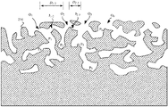
- FIG. 6 illustrates an exemplary electron microscope image of an etched part, in accordance with some embodiments.
- FIG. 6 illustrates a top-down image of an etched part 600 .
- the etched part 600 may correspond to the cleaned etched part 240 .
- the etched part 600 includes titanium and/or is formed from a titanium alloy.
- randomly-distributed openings e.g., O 1 , O 2 , O 3 —are formed throughout an external surface 602 of the etched part 600 .
- the openings are between about 1 micrometer to about 10 micrometers in diameter.
- FIG. 6 illustrates an exemplary electron microscope image of an etched part, in accordance with some embodiments.
- FIG. 6 illustrates a top-down image of an etched part 600 .
- the etched part 600 may correspond to the cleaned etched part 240 .
- the etched part 600 includes titanium and/or is formed from a titanium alloy.
- randomly-distributed openings e.g., O 1
- the external surface 602 is textured and etched such that different portions of the external surface 602 have different heights.
- the non-uniform and textured nature of the external surface 602 may promote greater bonding between the etched part 600 and a non-metal layer—e.g., the non-metal layer 252 .
- the external surface 602 is characterized as having a sponge-like network of channels on a scale of several microns (e.g., less than 10 micrometers in diameter). It should be noted that the openings—e.g., O 1 , O 2 , O 3 —of the external surface 602 of the etched part 600 are the result of an electrochemical etching process and not a blasting or slight roughening process.
- FIG. 7 illustrates an exemplary magnified electron microscope image of the region X of the etched part 600 , in accordance with some embodiments.
- the external surface 602 of the etched part 600 exhibits fine-scale (sub-micron) roughness and porosity of channels.
- the result is that the external surface 602 may be characterized as having a complex, three-dimensional labyrinth of openings that are interconnected to each other.
- FIG. 7 further illustrates an opening O 4 .
- FIG. 8 illustrates an exemplary cross-sectional view of an electron microscope image of a multi-layer part, in accordance with some embodiments.
- the multi-layer part 800 includes a metal part 802 that is bonded to a non-metal part 804 .
- the metal part 802 corresponds to a part that has been exposed to an electrochemical etching process, such as the cleaned etched part 240 .
- the metal part 802 includes openings that lead into channels. The channels are interconnected to each other.
- the walls 806 are etched to have textured surfaces with fine scale (sub-micron) roughness.
- the interconnected channels of the metal part 802 is of sufficient scale for penetration by protruding features of the non-metal part 804 .
- the channels may be referred to as interlocking structures due to the capability of the channels to enable interlocking between the metal part 802 and the non-metal part 804 .
- it is preferable that the channels are capable of exerting a significant amount of attachment strength onto the protruding features of the non-metal part 804 such as to prevent the non-metal part 804 from becoming forcefully pulled away from the metal part 802 .
- the non-metal part 804 includes protruding features 810 that extend through the openings of the metal part and fill in the channels. Subsequently, the penetration by the polymer material allows for mechanical interlocking between the metal part 802 and the non-metal part 804 .
- etching of the external surface of the metal part 802 may reduce the hardness of the metal part 802 , it should be noted that when the multi-layer part 800 is subjected to a pull strength test, that the non-metal material of the non-metal part 804 is more likely to fail first before the metal part 802 and the interface between the metal and non-metal parts 802 , 804 .
- any ranges cited herein are inclusive.
- the terms “substantially”, “generally,” and “about” used herein are used to describe and account for small fluctuations. For example, they can refer to less than or equal to ⁇ 5%, such as less than or equal to ⁇ 2%, such as less than or equal to ⁇ 1%, such as less than or equal to ⁇ 0.5%, such as less than or equal to ⁇ 0.1%.
- the various aspects, embodiments, implementations or features of the described embodiments can be used separately or in any combination.
- Various aspects of the described embodiments can be implemented by software, hardware or a combination of hardware and software.
- the described embodiments can also be embodied as computer readable code on a non-transitory computer readable medium.
- the non-transitory computer readable medium is any data storage device that can store data which can thereafter be read by a computer system. Examples of the non-transitory computer readable medium include read-only memory, random-access memory, CD-ROMs, HDDs, DVDs, magnetic tape, and optical data storage devices.
- the non-transitory computer readable medium can also be distributed over network-coupled computer systems so that the computer readable code is stored and executed in a distributed fashion.
Landscapes
- Chemical & Material Sciences (AREA)
- Engineering & Computer Science (AREA)
- Chemical Kinetics & Catalysis (AREA)
- Electrochemistry (AREA)
- Materials Engineering (AREA)
- Metallurgy (AREA)
- Organic Chemistry (AREA)
- ing And Chemical Polishing (AREA)
- Microelectronics & Electronic Packaging (AREA)
Abstract
Description
Claims (20)
Priority Applications (3)
| Application Number | Priority Date | Filing Date | Title |
|---|---|---|---|
| US16/867,200 US11511519B2 (en) | 2019-07-08 | 2020-05-05 | Titanium part having an etched surface |
| CN202311231378.8A CN117279249A (en) | 2019-07-08 | 2020-05-29 | Titanium parts with etched surfaces |
| CN202010471597.3A CN112203444A (en) | 2019-07-08 | 2020-05-29 | Titanium parts with etched surfaces |
Applications Claiming Priority (2)
| Application Number | Priority Date | Filing Date | Title |
|---|---|---|---|
| US201962871594P | 2019-07-08 | 2019-07-08 | |
| US16/867,200 US11511519B2 (en) | 2019-07-08 | 2020-05-05 | Titanium part having an etched surface |
Publications (2)
| Publication Number | Publication Date |
|---|---|
| US20210010151A1 US20210010151A1 (en) | 2021-01-14 |
| US11511519B2 true US11511519B2 (en) | 2022-11-29 |
Family
ID=74101945
Family Applications (1)
| Application Number | Title | Priority Date | Filing Date |
|---|---|---|---|
| US16/867,200 Active 2040-12-02 US11511519B2 (en) | 2019-07-08 | 2020-05-05 | Titanium part having an etched surface |
Country Status (1)
| Country | Link |
|---|---|
| US (1) | US11511519B2 (en) |
Families Citing this family (3)
| Publication number | Priority date | Publication date | Assignee | Title |
|---|---|---|---|---|
| CN110962280B (en) * | 2018-09-28 | 2021-09-03 | 比亚迪股份有限公司 | Metal-resin composite, preparation method thereof and electronic product shell |
| US11511519B2 (en) * | 2019-07-08 | 2022-11-29 | Apple Inc. | Titanium part having an etched surface |
| CN116837435A (en) * | 2022-03-23 | 2023-10-03 | 富联裕展科技(深圳)有限公司 | Electrochemical etching method for metal composite part |
Citations (18)
| Publication number | Priority date | Publication date | Assignee | Title |
|---|---|---|---|---|
| US20100272963A1 (en) * | 2009-04-27 | 2010-10-28 | Shenzhen Futaihong Precision Industry Co., Ltd. | Housing having woven appearance and manufacturing method thereof |
| US20110041553A1 (en) | 2009-08-18 | 2011-02-24 | Shenzhen Futaihong Precision Industry Co., Ltd. | Method for inlaying gold ornament and housing made by the method |
| US20110050055A1 (en) | 2009-08-28 | 2011-03-03 | Shenzhen Futaihong Precision Industry Co., Ltd. | Method for making device housing and device housing thereof |
| CN102480880A (en) | 2010-11-30 | 2012-05-30 | 深圳庆和胶粘制品有限公司 | Metal shell and preparation method and application thereof |
| CN102480879A (en) | 2010-11-26 | 2012-05-30 | 鸿富锦精密工业(深圳)有限公司 | Aluminum product and preparation method thereof |
| US20120229961A1 (en) | 2011-03-11 | 2012-09-13 | Fih (Hong Kong) Limited | Housing of electronic device and method for making the same |
| CN103068198A (en) | 2011-10-21 | 2013-04-24 | 深圳富泰宏精密工业有限公司 | Electronic device housing case and manufacturing method thereof |
| US20130108813A1 (en) | 2011-10-31 | 2013-05-02 | Fih (Hong Kong) Limited | Housing for electronic device and method of fabrication |
| CN104066283A (en) | 2013-03-21 | 2014-09-24 | 深圳富泰宏精密工业有限公司 | Housing and manufacture method thereof |
| CN105522684A (en) | 2014-12-25 | 2016-04-27 | 比亚迪股份有限公司 | Metal-resin composite as well as preparation method thereof and electronic product shell |
| CN105522682A (en) | 2014-12-25 | 2016-04-27 | 比亚迪股份有限公司 | Hyper-elastic nickel-titanium alloy-elastic resin composite, hyper-elastic nickel-titanium alloy substrate, preparation method for composite and electronic product shell |
| CN105522683A (en) | 2014-12-25 | 2016-04-27 | 比亚迪股份有限公司 | Nickel-titanium alloy substrate subjected to surface treatment, nickel-titanium alloy-resin composite, preparation method for composite and electronic product shell |
| US9746765B2 (en) | 2013-11-08 | 2017-08-29 | Lg Electronics Inc. | Exterior décor panel for home appliance and method of manufacturing the same |
| CN109023497A (en) | 2017-06-09 | 2018-12-18 | 深圳富泰宏精密工业有限公司 | The production method of shell and the shell |
| US20190069076A1 (en) | 2017-08-31 | 2019-02-28 | Apple Inc. | Micro speaker having a hermetically sealed acoustic chamber with increased volume |
| CN109475056A (en) | 2017-09-08 | 2019-03-15 | 苹果公司 | For polymer material to be bonded to the etching of anodized metal |
| US20190098785A1 (en) | 2017-09-08 | 2019-03-28 | Apple Inc. | Etching for bonding polymer material to a metal surface |
| US20210010151A1 (en) * | 2019-07-08 | 2021-01-14 | Apple Inc. | Titanium part having an etched surface |
-
2020
- 2020-05-05 US US16/867,200 patent/US11511519B2/en active Active
Patent Citations (26)
| Publication number | Priority date | Publication date | Assignee | Title |
|---|---|---|---|---|
| US20100272963A1 (en) * | 2009-04-27 | 2010-10-28 | Shenzhen Futaihong Precision Industry Co., Ltd. | Housing having woven appearance and manufacturing method thereof |
| US20110041553A1 (en) | 2009-08-18 | 2011-02-24 | Shenzhen Futaihong Precision Industry Co., Ltd. | Method for inlaying gold ornament and housing made by the method |
| CN101992651A (en) | 2009-08-18 | 2011-03-30 | 深圳富泰宏精密工业有限公司 | Gold inlaying method and gold-inlaid electronic device shell prepared thereby |
| US20110050055A1 (en) | 2009-08-28 | 2011-03-03 | Shenzhen Futaihong Precision Industry Co., Ltd. | Method for making device housing and device housing thereof |
| CN102006753A (en) | 2009-08-28 | 2011-04-06 | 深圳富泰宏精密工业有限公司 | Shell making method and shell made by same |
| CN102480879A (en) | 2010-11-26 | 2012-05-30 | 鸿富锦精密工业(深圳)有限公司 | Aluminum product and preparation method thereof |
| US20120135222A1 (en) | 2010-11-26 | 2012-05-31 | Hon Hai Precision Industry Co., Ltd. | Aluminum article and method for manufacturing same |
| CN102480880A (en) | 2010-11-30 | 2012-05-30 | 深圳庆和胶粘制品有限公司 | Metal shell and preparation method and application thereof |
| US20120229961A1 (en) | 2011-03-11 | 2012-09-13 | Fih (Hong Kong) Limited | Housing of electronic device and method for making the same |
| CN102686075A (en) | 2011-03-11 | 2012-09-19 | 深圳富泰宏精密工业有限公司 | Electronic device casing and manufacturing method thereof |
| CN103068198A (en) | 2011-10-21 | 2013-04-24 | 深圳富泰宏精密工业有限公司 | Electronic device housing case and manufacturing method thereof |
| US20130101765A1 (en) | 2011-10-21 | 2013-04-25 | Fih (Hong Kong) Limited | Device housing and method for making the same |
| US20130108813A1 (en) | 2011-10-31 | 2013-05-02 | Fih (Hong Kong) Limited | Housing for electronic device and method of fabrication |
| CN103096650A (en) | 2011-10-31 | 2013-05-08 | 深圳富泰宏精密工业有限公司 | Electronic device shell and manufacture method thereof |
| CN104066283A (en) | 2013-03-21 | 2014-09-24 | 深圳富泰宏精密工业有限公司 | Housing and manufacture method thereof |
| US20140284071A1 (en) | 2013-03-21 | 2014-09-25 | Fih (Hong Kong) Limited | Housing and method for manufacturing the same |
| US9746765B2 (en) | 2013-11-08 | 2017-08-29 | Lg Electronics Inc. | Exterior décor panel for home appliance and method of manufacturing the same |
| CN105522684A (en) | 2014-12-25 | 2016-04-27 | 比亚迪股份有限公司 | Metal-resin composite as well as preparation method thereof and electronic product shell |
| CN105522683A (en) | 2014-12-25 | 2016-04-27 | 比亚迪股份有限公司 | Nickel-titanium alloy substrate subjected to surface treatment, nickel-titanium alloy-resin composite, preparation method for composite and electronic product shell |
| CN105522682A (en) | 2014-12-25 | 2016-04-27 | 比亚迪股份有限公司 | Hyper-elastic nickel-titanium alloy-elastic resin composite, hyper-elastic nickel-titanium alloy substrate, preparation method for composite and electronic product shell |
| US20170282424A1 (en) | 2014-12-25 | 2017-10-05 | Byd Company Limited | Metal-resin composite and method of preparing the same and shell of electronic product |
| CN109023497A (en) | 2017-06-09 | 2018-12-18 | 深圳富泰宏精密工业有限公司 | The production method of shell and the shell |
| US20190069076A1 (en) | 2017-08-31 | 2019-02-28 | Apple Inc. | Micro speaker having a hermetically sealed acoustic chamber with increased volume |
| CN109475056A (en) | 2017-09-08 | 2019-03-15 | 苹果公司 | For polymer material to be bonded to the etching of anodized metal |
| US20190098785A1 (en) | 2017-09-08 | 2019-03-28 | Apple Inc. | Etching for bonding polymer material to a metal surface |
| US20210010151A1 (en) * | 2019-07-08 | 2021-01-14 | Apple Inc. | Titanium part having an etched surface |
Also Published As
| Publication number | Publication date |
|---|---|
| US20210010151A1 (en) | 2021-01-14 |
Similar Documents
| Publication | Publication Date | Title |
|---|---|---|
| US11511519B2 (en) | Titanium part having an etched surface | |
| JP6778724B2 (en) | Etching to bond polymer material to anodized metal | |
| US9152038B2 (en) | Photomasks and methods for using same | |
| KR102294459B1 (en) | Textured surface for titanium parts | |
| US11178781B2 (en) | Etching for bonding polymer material to a metal surface | |
| US20180086662A1 (en) | Process for forming textured glass component with high bending strength | |
| CN117279249A (en) | Titanium parts with etched surfaces | |
| JP2016510364A (en) | Method for improving adhesion of aluminum film | |
| TWI581330B (en) | A component having better plasma etch resistance and a method of improving the resistance of the component to plasma etching | |
| CN110528046B (en) | Method for forming metal surface texture, metal shell and electronic device | |
| CN206559776U (en) | The anodized substrate of white appearance and the housing for electronic equipment | |
| TWI418284B (en) | Shell of electronic device and method for manufacturing the same | |
| CN110886000A (en) | Corrosion resistance of anodized parts with convex features | |
| Calota et al. | Investigation of chemical/mechanical polishing of niobium | |
| CN114686948A (en) | Method for forming hole, metal workpiece and metal product | |
| JP2006114929A (en) | Polishing method | |
| JPS63166993A (en) | Production of substrate for magnetic disk |
Legal Events
| Date | Code | Title | Description |
|---|---|---|---|
| AS | Assignment |
Owner name: APPLE INC., CALIFORNIA Free format text: ASSIGNMENT OF ASSIGNORS INTEREST;ASSIGNORS:CURRAN, JAMES A.;MINTZ, TODD S.;YANG, ISABEL;REEL/FRAME:052575/0638 Effective date: 20200422 |
|
| FEPP | Fee payment procedure |
Free format text: ENTITY STATUS SET TO UNDISCOUNTED (ORIGINAL EVENT CODE: BIG.); ENTITY STATUS OF PATENT OWNER: LARGE ENTITY |
|
| STPP | Information on status: patent application and granting procedure in general |
Free format text: APPLICATION DISPATCHED FROM PREEXAM, NOT YET DOCKETED |
|
| STPP | Information on status: patent application and granting procedure in general |
Free format text: DOCKETED NEW CASE - READY FOR EXAMINATION |
|
| STPP | Information on status: patent application and granting procedure in general |
Free format text: NON FINAL ACTION MAILED |
|
| STPP | Information on status: patent application and granting procedure in general |
Free format text: RESPONSE TO NON-FINAL OFFICE ACTION ENTERED AND FORWARDED TO EXAMINER |
|
| STPP | Information on status: patent application and granting procedure in general |
Free format text: NOTICE OF ALLOWANCE MAILED -- APPLICATION RECEIVED IN OFFICE OF PUBLICATIONS |
|
| STPP | Information on status: patent application and granting procedure in general |
Free format text: PUBLICATIONS -- ISSUE FEE PAYMENT VERIFIED |
|
| STCF | Information on status: patent grant |
Free format text: PATENTED CASE |