US11500408B2 - Reference voltage circuit - Google Patents
Reference voltage circuit Download PDFInfo
- Publication number
- US11500408B2 US11500408B2 US17/158,379 US202117158379A US11500408B2 US 11500408 B2 US11500408 B2 US 11500408B2 US 202117158379 A US202117158379 A US 202117158379A US 11500408 B2 US11500408 B2 US 11500408B2
- Authority
- US
- United States
- Prior art keywords
- mos transistor
- terminal
- circuit
- voltage
- current
- Prior art date
- Legal status (The legal status is an assumption and is not a legal conclusion. Google has not performed a legal analysis and makes no representation as to the accuracy of the status listed.)
- Active, expires
Links
Images


Classifications
-
- G—PHYSICS
- G05—CONTROLLING; REGULATING
- G05F—SYSTEMS FOR REGULATING ELECTRIC OR MAGNETIC VARIABLES
- G05F1/00—Automatic systems in which deviations of an electric quantity from one or more predetermined values are detected at the output of the system and fed back to a device within the system to restore the detected quantity to its predetermined value or values, i.e. retroactive systems
- G05F1/10—Regulating voltage or current
- G05F1/46—Regulating voltage or current wherein the variable actually regulated by the final control device is dc
- G05F1/56—Regulating voltage or current wherein the variable actually regulated by the final control device is dc using semiconductor devices in series with the load as final control devices
- G05F1/565—Regulating voltage or current wherein the variable actually regulated by the final control device is dc using semiconductor devices in series with the load as final control devices sensing a condition of the system or its load in addition to means responsive to deviations in the output of the system, e.g. current, voltage, power factor
- G05F1/567—Regulating voltage or current wherein the variable actually regulated by the final control device is dc using semiconductor devices in series with the load as final control devices sensing a condition of the system or its load in addition to means responsive to deviations in the output of the system, e.g. current, voltage, power factor for temperature compensation
-
- G—PHYSICS
- G05—CONTROLLING; REGULATING
- G05F—SYSTEMS FOR REGULATING ELECTRIC OR MAGNETIC VARIABLES
- G05F3/00—Non-retroactive systems for regulating electric variables by using an uncontrolled element, or an uncontrolled combination of elements, such element or such combination having self-regulating properties
- G05F3/02—Regulating voltage or current
- G05F3/08—Regulating voltage or current wherein the variable is dc
- G05F3/10—Regulating voltage or current wherein the variable is dc using uncontrolled devices with non-linear characteristics
- G05F3/16—Regulating voltage or current wherein the variable is dc using uncontrolled devices with non-linear characteristics being semiconductor devices
- G05F3/20—Regulating voltage or current wherein the variable is dc using uncontrolled devices with non-linear characteristics being semiconductor devices using diode- transistor combinations
- G05F3/24—Regulating voltage or current wherein the variable is dc using uncontrolled devices with non-linear characteristics being semiconductor devices using diode- transistor combinations wherein the transistors are of the field-effect type only
- G05F3/242—Regulating voltage or current wherein the variable is dc using uncontrolled devices with non-linear characteristics being semiconductor devices using diode- transistor combinations wherein the transistors are of the field-effect type only with compensation for device parameters, e.g. channel width modulation, threshold voltage, processing, or external variations, e.g. temperature, loading, supply voltage
-
- G—PHYSICS
- G05—CONTROLLING; REGULATING
- G05F—SYSTEMS FOR REGULATING ELECTRIC OR MAGNETIC VARIABLES
- G05F3/00—Non-retroactive systems for regulating electric variables by using an uncontrolled element, or an uncontrolled combination of elements, such element or such combination having self-regulating properties
- G05F3/02—Regulating voltage or current
- G05F3/08—Regulating voltage or current wherein the variable is dc
- G05F3/10—Regulating voltage or current wherein the variable is dc using uncontrolled devices with non-linear characteristics
- G05F3/16—Regulating voltage or current wherein the variable is dc using uncontrolled devices with non-linear characteristics being semiconductor devices
- G05F3/20—Regulating voltage or current wherein the variable is dc using uncontrolled devices with non-linear characteristics being semiconductor devices using diode- transistor combinations
- G05F3/26—Current mirrors
- G05F3/262—Current mirrors using field-effect transistors only
-
- G—PHYSICS
- G05—CONTROLLING; REGULATING
- G05F—SYSTEMS FOR REGULATING ELECTRIC OR MAGNETIC VARIABLES
- G05F3/00—Non-retroactive systems for regulating electric variables by using an uncontrolled element, or an uncontrolled combination of elements, such element or such combination having self-regulating properties
- G05F3/02—Regulating voltage or current
- G05F3/08—Regulating voltage or current wherein the variable is dc
Definitions
- the present invention relates to a reference voltage circuit.
- a reference voltage circuit formed on a semiconductor chip is used, and is accordingly required to have an output voltage that is stable irrespective of fluctuations in ambient temperature and in power supply voltage, and to operate on minute power.
- a widely used reference voltage circuit is a band gap reference circuit (hereinafter referred to as “BGR circuit”).
- the BGR circuit utilizes characteristics in which a collector current is in proportion to an exponent of a base-emitter voltage and an area of the emitter, to thereby have an advantage of being able to generate a voltage at which a first-order temperature coefficient is zero.
- the BGR circuit is therefore widely used as a reference voltage circuit.
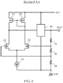
- a reference voltage circuit illustrated in FIG. 6 includes NMOS transistors 21 and 22 , PMOS transistors 23 and 24 , a current source circuit 25 , resistors 27 to 29 , and an output circuit 26 .
- the NMOS transistors 21 and 22 form a differential amplifier.
- the NMOS transistors 21 and 22 have different threshold values or the same threshold value and different channel width (W).
- This circuit generates a desired output voltage VOUT by adjusting, with a resultant input offset voltage of the differential amplifier, namely, a voltage between terminals of the resistor 28 , being used as a reference, the ratio of resistance values among the resistor 27 , the resistor 28 , and the resistor 29 (see Japanese Patent Application Laid-open No. Hei 3-180915, for example).
- a reference voltage circuit used in an IoT device or the like is required to operate on minute power and generate a voltage that is stable irrespective of fluctuations in ambient temperature and in power supply voltage.
- the reference voltage circuit of the present invention includes MOS transistors, operates on a minute current, and can generate a voltage that is as stable as that of a BGR circuit of the related art with respect to temperature fluctuations and fluctuations in power supply voltage.
- FIG. 1 is a circuit diagram for illustrating a configuration of a reference voltage circuit of a first embodiment of the present invention.
- FIG. 2 is a circuit diagram for illustrating a configuration of a reference voltage circuit of a second embodiment of the present invention.
- FIG. 3 is a circuit diagram for illustrating a configuration of a reference voltage circuit of a third embodiment of the present invention.
- FIG. 4 is a graph for showing characteristics of the reference voltage circuits of the first to third embodiments.
- FIG. 5 is a graph for showing characteristics of the reference voltage circuits of the first to third embodiments.
- FIG. 6 is a circuit diagram for illustrating a configuration of a reference voltage circuit of the related art.
- a reference voltage circuit of a first embodiment of the present invention is described with reference to FIG. 1 .
- the reference voltage circuit of the first embodiment includes NMOS transistors 1 to 3 , PMOS transistors 4 to 6 , resistors 7 and 8 , a current source circuit 9 , a capacitor 10 , a power supply terminal 13 , a GND terminal, and an output terminal 14 .
- a power supply voltage VDD is supplied through the power supply terminal 13 .
- the GND terminal is set to a GND potential.
- An output voltage V REF1 is output through the output terminal 14 .
- the NMOS transistor 1 has a drain terminal connected to a connection point n 1 , a gate terminal connected to a connection point n 3 , and a source terminal connected to a first terminal of the current source circuit 9 .
- the NMOS transistor 2 has a drain terminal connected to a connection point n 2 , a gate terminal connected to a connection point n 4 , and a source terminal connected to the first terminal of the current source circuit 9 .
- the current source circuit 9 has a second terminal connected to the GND terminal.
- the NMOS transistor 3 has a drain terminal and a gate terminal that are connected to the connection point n 4 , and a source terminal connected to the GND terminal.
- the NMOS transistors 1 to 3 each have a back gate terminal connected to the GND terminal.
- the PMOS transistor 4 has a source terminal connected to the power supply terminal 13 , and a gate terminal and a drain terminal that are connected to the connection point n 1 .
- the PMOS transistor 5 has a gate terminal connected to the connection point n 1 , a source terminal connected to the power supply terminal 13 , and a drain terminal connected to the connection point n 2 .
- the PMOS transistor 6 has a source terminal connected to the power supply terminal 13 , a gate terminal connected to the connection point n 2 , and a drain terminal connected to the output terminal 14 and to a first terminal of the resistor 8 .
- the PMOS transistors 4 to 6 each have a back gate terminal connected to the power supply terminal 13 .
- the resistor 7 has a first terminal connected to the connection point n 3 , and a second terminal connected to the connection point n 4 .
- the resistor 8 has a second terminal connected to the connection point n 3 .
- the capacitor 10 has a first terminal connected to the power supply terminal 13 and a second terminal connected to the connection point n 2 .
- the NMOS transistors 1 and 2 , the PMOS transistors 4 to 6 , the current source circuit 9 , and the capacitor 10 form a differential amplifier 12 .
- the NMOS transistors 1 and 2 are input transistors, and are driven by the current source circuit 9 in a weak inversion region.
- the NMOS transistors 1 and 2 are equal to each other in channel length (L), and are set to a channel width (W) ratio of 1:M.
- the capacitor 10 is a phase compensation capacitor for achieving a stable feedback loop.
- the PMOS transistors 4 to 6 form an output stage of the differential amplifier 12 .
- the PMOS transistors 4 to 6 are equal to one another in channel length (L) and channel width (W) both.
- the PMOS transistors 4 and 5 form a current minor circuit.
- the PMOS transistor 4 is diode-connected.
- a current I 1 flowing in the PMOS transistor 4 flows into the NMOS transistor 1 .
- a current I 2 is copied as a mirror of the current I 1 by the PMOS transistor 5 , and flows into the NMOS transistor 2 .
- a voltage between the gate terminal and source terminal of the NMOS transistor 1 is referred to as “voltage V gs1 ”, and a voltage between the gate terminal and source terminal of the NMOS transistor 2 is referred to as “voltage V gs2 ”.
- a voltage V n2 obtained by amplifying a voltage that is a difference between the voltage V gs1 and the voltage V gs2 is generated at the connection point n 2 .
- the PMOS transistor 6 converts the voltage V n2 into a current I 3 and outputs the current I 3 .
- the differential amplifier 12 operates as a transconductance amplifier configured to amplify the voltage that is a difference between the voltage V gs1 and the voltage V gs2 and convert the amplified voltage into the current I 3 .
- the current I 3 output from the differential amplifier 12 flows into the GND terminal via the resistor 8 , the resistor 7 , and the diode-connected NMOS transistor 3 .
- the current I 3 causes generation of a voltage V R1 between terminals of the resistor 7 and generation of a voltage V R2 between terminals of the resistor 8 .
- the connection point n 3 is connected to the gate terminal of the NMOS transistor 1
- the connection point n 4 is connected to the gate terminal of the NMOS transistor 2 .
- a feedback loop in which the current I 3 is converted at the resistor 7 into the voltage V R1 to be returned to input is formed.
- the current I 3 output from the differential amplifier 12 is fed back to input of the differential amplifier 12 .
- the reference voltage circuit of the first embodiment is stable when a voltage at the drain terminal of the NMOS transistor 1 and a voltage at the drain terminal of the NMOS transistor 2 are equal to each other, and the current I 1 , the current I 2 , and the current I 3 are equal to one another.
- the NMOS transistor 1 and the NMOS transistor 2 are driven by the current source circuit 9 to operate in a weak inversion region.
- a MOS transistor operating in a weak inversion region is expressed, as indicated by Expression (2), in a form in which a drain current I d is in proportion to an exponent of a gate-source voltage V gs .
- This relationship is known to be a characteristic close to the relationship of the collector current of a bipolar transistor to the base-emitter voltage which is used as a reference of the voltage in the BGR circuit of the related art. That is, this property can be utilized to generate, with the use of a MOS transistor, a reference voltage that is stable with respect to temperature changes as in a BGR circuit of the related art, without using a bipolar transistor.
- k represents the Boltzmann constant of 1.38E-23 [J/K]
- T the absolute temperature [K]
- n a slope factor (a constant, normally from about 1 to 2)
- I s represents a constant determined by process
- V gs represents the gate-source voltage
- V th represents a threshold voltage of the MOS transistor.
- the NMOS transistor 1 and the NMOS transistor 2 are equal to each other in threshold voltage V th and channel length (L).
- the channel width (W) of the NMOS transistor 1 is denoted by W 1 and the channel width (W) of the NMOS transistor 2 is denoted by W 2 .
- the ratio of the channel width W 1 and the channel width W 2 is 1:M.
- the current I 1 is a current which flows in the NMOS transistor 1 in the differential amplifier 12 .
- the current I 2 is a current which flows in the NMOS transistor 2 in the differential amplifier 12 .
- Each of the current I 1 and the current I 2 is expressed by Expression (3) and Expression (4) because the NMOS transistors 1 and 2 operate in a weak inversion region.
- V gs1 represents the gate-source voltage of the NMOS transistor 1 .
- V gs2 represents the gate-source voltage of the NMOS transistor 2 .
- V th represents a threshold voltage of the NMOS transistors 1 and 2 .
- the voltage V R1 between the terminals of the resistor 7 is a voltage that is a difference between the voltage V gs1 of the NMOS transistor 1 and the voltage V gs2 of the NMOS transistor 2 .
- Expression (5) which expresses the voltage V R1 , is derived from Expression (3) and Expression (4).
- the current I 3 is a current flowing in the resistor 7 and is expressed by Expression (6).
- R 1 represents the resistance value of the resistor 7 .
- the current I 3 is a proportional-to-absolute-temperature (PTAT) current, and is proportional to the absolute temperature T.
- PTAT proportional-to-absolute-temperature
- the current I 1 and the current I 2 start to change because the absolute temperature T is included in the right-hand side of each of Expression (3) as to the current I 1 and Expression (4) as to the current I 2 .
- the current I 3 is a PTAT current, and accordingly the voltage V R1 between the terminals of the resistor 7 in which the current I 3 flows changes, and the voltage V gs1 of the NMOS transistor 1 and the voltage V gs2 of the NMOS transistor 2 change.
- the current I 1 and the current I 2 consequently become equal to each other, and the sum of the current I 1 and the current I 2 settles to a current value set by the current source circuit 9 and is stabilized.
- the output voltage V REF1 of the reference voltage circuit of the first embodiment is the sum of a gate-source voltage V gs3 of the NMOS transistor 3 , the voltage V R1 between the terminals of the resistor 7 , and the voltage V R2 between the terminals of the resistor 8 , and is expressed by Expression (7).
- R 2 represents the resistance value of the resistor 8 .
- the gate-source voltage V gs3 which is the first term of Expression (7) is changed due to a temperature change generally by an amount that has a negative value of approximately ⁇ 0.5 mV/K to ⁇ 2 mV/K.
- the voltage V R1 between the terminals of the resistor 7 and the voltage V R2 between the terminals of the resistor 8 , each of which is the second term of Expression (7), have a positive temperature coefficient because the current I 3 is a PTAT current.
- a circuit constant may be appropriately adjusted so that a temperature-induced change of the gate-source voltage V gs3 of the NMOS transistor 3 is canceled out by temperature-induced changes of the voltage V R1 between the terminals of the resistor 7 and the voltage V R2 between the terminals of the resistor 8 .
- Expression (7) does not include a variable related to the power supply voltage VDD, and the output voltage V REF1 is accordingly stable with respect to fluctuations in power supply voltage as well.
- a condition for setting the first-order temperature coefficient of a temperature-induced fluctuation amount ⁇ V REF1 of the output voltage V REF1 from the reference voltage circuit of the first embodiment to zero becomes clear from Expression (8) obtained by differentiating Expression (7) by the absolute temperature T.
- ⁇ ⁇ V REF ⁇ 1 ⁇ V gs ⁇ 3 ⁇ T + n ⁇ R 1 + R 2 R 1 ⁇ k q ⁇ ln ⁇ ( M ) ( 8 )
- the condition for setting the first-order temperature coefficient of the temperature-induced fluctuation amount ⁇ V REF1 to zero may be obtained by adjusting the value of (R 1 +R 2 )/R 1 and the value of M to appropriate values so that the first term of Expression (8) is canceled out by the second term of Expression (8).
- the value of M is the ratio of the NMOS transistor 2 to the NMOS transistor 1 in channel width (W).
- the circuit current is determined by the current source circuit 9 .
- TC 1 represents a first-order temperature coefficient of the resistors.
- a curve 15 of FIG. 4 indicates temperature characteristics of the output voltage V REF1 that is observed in the reference voltage circuit of the first embodiment when the power supply voltage VDD is 3 V.
- a curve 18 of FIG. 5 indicates dependence of the output voltage V REF1 on the power supply voltage VDD that is observed in the reference voltage circuit of the first embodiment when the temperature is 25° C. (298 K).
- the output voltage V REF1 changes by 7.2 mV when the power supply voltage VDD changes from 1.2 V to 5 V.
- a reference voltage circuit of a second embodiment of the present invention is described with reference to FIG. 2 .
- the reference voltage circuit illustrated in FIG. 2 has a configuration in which the current source circuit 9 of the reference voltage circuit of the first embodiment is replaced with an NMOS transistor 11 .
- the NMOS transistor 11 has a drain terminal connected to the source terminal of the NMOS transistor 1 and the source terminal of the NMOS transistor 2 , a gate terminal connected to the gate terminal of the NMOS transistor 3 , and a source terminal and a back gate terminal that are connected to the GND terminal.
- the reference voltage circuit of the second embodiment is a circuit having a self-biased configuration that uses a current mirror circuit formed from the NMOS transistor 3 and the NMOS transistor 11 to feed the current I 3 on which the differential amplifier 12 itself is driven. Further, the current I 3 is supplied from the differential amplifier 12 and fed back as a current I 02 .
- the reference voltage circuit of the second embodiment outputs the output voltage V REF1 .
- the channel width (W) of the NMOS transistor 11 is set to twice the channel width (W) of the NMOS transistor 3 , and the current I 02 is accordingly twice larger than the current I 3 .
- a conditional expression for setting the first-order temperature coefficient of ⁇ V REF1 to zero in the reference voltage circuit of the second embodiment is the same as that in the reference voltage circuit of the first embodiment.
- the current source circuit 9 of the reference voltage circuit of the first embodiment has a constant current
- the current I 02 of the reference voltage circuit of the second embodiment is a current proportional to the absolute temperature because the current I 02 is a feedback current of the PTAT current I 3 that is fed back by the current mirror circuit formed from the NMOS transistor 3 and the NMOS transistor 11 .
- a circuit constant that sets the first-order temperature coefficient of the output voltage to zero therefore takes a value different from that in the circuit of the first embodiment as in an example described later.
- a curve 16 of FIG. 4 indicates temperature characteristics of the output voltage V REF1 that is observed in the reference voltage circuit of the second embodiment when the power supply voltage VDD is 3 V.
- the output voltage V REF1 is 1.148 V at 25° C., and a fluctuation range of the output voltage V REF1 in a temperature range of from ⁇ 20° C. to 100° C. is 7.10 mV.
- a curve 19 of FIG. 5 indicates dependence of the output voltage V REF1 on the power supply voltage VDD that is observed in the reference voltage circuit of the second embodiment when the temperature is 25° C. (298 K).
- the output voltage V REF1 changes by 6.8 mV when the power supply voltage VDD changes from 1.2 V to 5 V.
- a reference voltage circuit of a third embodiment of the present invention is described with reference to FIG. 3 .
- the reference voltage circuit of the third embodiment is a circuit obtained by changing a place in which the gate terminal of the NMOS transistor 3 in the reference voltage circuit of the second embodiment is connected.
- the difference from the reference voltage circuit of the second embodiment is that the gate terminal of the NMOS transistor 3 is connected to the connection point n 3 between the resistor 7 , the resistor 8 , and the gate terminal of the NMOS transistor 1 .
- the reference voltage circuit of the third embodiment outputs an output voltage V REF2 .
- the current source circuit illustrated in FIG. 3 as the current source circuit in the third embodiment has the same circuit configuration as that in the second embodiment, but may have the same circuit configuration as that in the first embodiment.
- An output voltage in that case differs from the output voltage of the current source circuit in the third embodiment has the same circuit configuration as that in the second embodiment as with the output voltage of the first embodiment and the output voltage of the second embodiment which differ from each other.
- the NMOS transistor 3 and the NMOS transistor 11 form a current mirror circuit in which, as in the second embodiment, the channel width (W) of the NMOS transistor 11 is set to twice the channel width (W) of the NMOS transistor 3 , and the current I 02 is accordingly twice larger than the current I 3 .
- a potential at the connection point n 3 is fixed to the gate-source voltage V gs3 of the NMOS transistor 3 , and the connection point n 3 is accordingly kept to a voltage that is lower than that in the reference voltage circuit of the second embodiment.
- the reference voltage circuit of the third embodiment is therefore required to adjust the channel length (L) and channel width (W) of the NMOS transistor 3 so that the gate-source voltage V gs3 of the NMOS transistor 3 is high enough for the NMOS transistor 1 , the NMOS transistor 2 , and the NMOS transistor 11 to operate well.
- the reference voltage circuit of the third embodiment controls the NMOS transistor 3 (and the NMOS transistor 11 ) to operate in a saturation region, and thus sets V gs3 of the NMOS transistor 3 to a voltage that is higher than the threshold voltage V th by about 0.3 V.
- the output voltage V REF2 of the reference voltage circuit of the third embodiment is a voltage that is the sum of the gate-source voltage V gs3 of the NMOS transistor 3 and the voltage V R2 between the terminals of the resistor 8 , and is expressed by Expression (9).
- a temperature-induced fluctuation amount ⁇ V REF2 of the output voltage V REF2 from the reference voltage circuit of the third embodiment is obtained by differentiating Expression (9) by the absolute temperature T.
- the temperature-induced fluctuation amount ⁇ V REF2 is expressed as Expression (10).
- ⁇ ⁇ V REF ⁇ 2 ⁇ V gs ⁇ 3 ⁇ T + n ⁇ R 2 R 1 ⁇ k q ⁇ ln ⁇ ( M ) ( 10 )
- the first term on the right-hand side of Expression (10), i.e., ( ⁇ V gs3 )/( ⁇ T) is a temperature-induced change amount of the gate-source voltage V gs3 of the NMOS transistor 3 .
- a first-order temperature coefficient of the output voltage V REF2 is set to zero by adjusting the value of (R 2 /R 1 ) and the value of M to appropriate values so that the first term of Expression (10) is canceled out by the second term of Expression (10).
- the value of M is the ratio of the NMOS transistor 2 to the NMOS transistor 1 in channel width (W). A reference voltage that is stable regardless of temperature fluctuations is thus obtained.
- a curve 17 of FIG. 4 indicates temperature characteristics of the output voltage V REF2 that is observed in the reference voltage circuit of the third embodiment when the power supply voltage VDD is 3 V.
- the output voltage V REF2 is 1.144 V at 25° C., and a fluctuation range of the output voltage V REF2 in a temperature range of from ⁇ 20° C. to 100° C. is 7.03 mV.
- a curve 20 of FIG. 5 indicates dependence of the output voltage V REF2 on the power supply voltage VDD that is observed in the reference voltage circuit of the third embodiment when the temperature is 25° C. (298 K).
- the output voltage V REF2 changes by 6.6 mV when the power supply voltage VDD changes from 1.2 V to 5 V.
- FIG. 4 is a graph for showing temperature characteristics of the output voltages V REF1 and V REF2 with the circuit configurations of the first to third embodiments when the power supply voltage VDD is 3 V.
- fluctuation ranges of the output voltages in a temperature range of from ⁇ 20° C. to 100° C. are equivalent to an output voltage fluctuation range in a BGR circuit of the related art, such as a BGR circuit including a bipolar transistor.
- FIG. 5 is a graph for showing characteristics of the output voltages V REF1 and V REF2 with respect to fluctuations of the power supply voltage VDD with the circuit configurations of the first to third embodiments at a temperature of 25° C.
- the circuit of any of the first to third embodiments has an output voltage that is substantially constant. This simulation result indicates that the circuits of the first to third embodiments keep output voltages stable and function as reference voltage circuits even when the power supply voltage VDD widely changes.
- the total current consumption is as small as 30 nA in the circuit of any of the first to third embodiments. Power consumed when the power supply voltage VDD is 1.5 V which is the voltage of a single dry-cell battery required to function as a reference voltage circuit is only 45 nW.
- the reference voltage circuits of the first to third embodiments operate on a minute current, and can generate a voltage that is as stable as that of a BGR circuit of the related art with respect to temperature fluctuations. That is, the reference voltage circuits of the first to third embodiments are reference voltage circuits that satisfy requirements of an IoT device at the same time.
- the channel widths (W) of the transistors may equivalently be varied by connecting a plurality of transistors in parallel and changing the number of transistors connected in parallel.
- the number of transistors connected in parallel can be changed by fabricating a large number of transistors in advance and removing some of the transistors by laser trimming or other methods.
- the operation has been described based on the circuits having a form in which the back gate of a MOS transistor is connected to the GND terminal or the power supply terminal 13 .
- the same characteristics are obtained even with a circuit having a form in which the back gate is connected to the drain of its own MOS transistor with the use of a special CMOS process that can separate the back gate from a substrate potential.
Abstract
Description
I 1 =I 2 I 3 (1)
Claims (6)
Applications Claiming Priority (3)
| Application Number | Priority Date | Filing Date | Title |
|---|---|---|---|
| JPJP2020-019709 | 2020-02-07 | ||
| JP2020-019709 | 2020-02-07 | ||
| JP2020019709A JP7325352B2 (en) | 2020-02-07 | 2020-02-07 | Reference voltage circuit |
Publications (2)
| Publication Number | Publication Date |
|---|---|
| US20210247794A1 US20210247794A1 (en) | 2021-08-12 |
| US11500408B2 true US11500408B2 (en) | 2022-11-15 |
Family
ID=77177973
Family Applications (1)
| Application Number | Title | Priority Date | Filing Date |
|---|---|---|---|
| US17/158,379 Active 2041-06-19 US11500408B2 (en) | 2020-02-07 | 2021-01-26 | Reference voltage circuit |
Country Status (3)
| Country | Link |
|---|---|
| US (1) | US11500408B2 (en) |
| JP (1) | JP7325352B2 (en) |
| CN (1) | CN113253788B (en) |
Families Citing this family (2)
| Publication number | Priority date | Publication date | Assignee | Title |
|---|---|---|---|---|
| CN112072900B (en) * | 2020-08-25 | 2021-07-09 | 苏州纳芯微电子股份有限公司 | Drive circuit of drive chip |
| CN114578891B (en) * | 2022-05-06 | 2022-07-12 | 苏州贝克微电子股份有限公司 | Circuit capable of reducing temperature influence |
Citations (4)
| Publication number | Priority date | Publication date | Assignee | Title |
|---|---|---|---|---|
| JPH03180915A (en) | 1989-12-08 | 1991-08-06 | Ricoh Co Ltd | Reference voltage generating circuit |
| US7135913B2 (en) * | 2003-10-29 | 2006-11-14 | Samsung Electronics Co., Ltd. | Reference voltage generating circuit for integrated circuit |
| US20100156386A1 (en) * | 2008-12-24 | 2010-06-24 | Takashi Imura | Reference voltage circuit |
| US10831228B2 (en) * | 2015-11-11 | 2020-11-10 | Apple Inc. | Apparatus and method for high voltage bandgap type reference circuit with flexible output setting |
Family Cites Families (8)
| Publication number | Priority date | Publication date | Assignee | Title |
|---|---|---|---|---|
| JPH03296118A (en) * | 1990-04-13 | 1991-12-26 | Oki Micro Design Miyazaki:Kk | Reference voltage generating circuit |
| KR100738964B1 (en) | 2006-02-28 | 2007-07-12 | 주식회사 하이닉스반도체 | Band-gap reference voltage generator |
| JP2007300760A (en) * | 2006-05-02 | 2007-11-15 | Rohm Co Ltd | Booster circuit and electric apparatus |
| JP2008004741A (en) * | 2006-06-22 | 2008-01-10 | Matsushita Electric Ind Co Ltd | Semiconductor integrated circuit, and information apparatus, communication apparatus, av apparatus and mobile unit comprising it |
| JP4746489B2 (en) * | 2006-06-28 | 2011-08-10 | 株式会社リコー | Semiconductor measuring equipment |
| JP2008152632A (en) | 2006-12-19 | 2008-07-03 | Ricoh Co Ltd | Reference voltage generation circuit |
| JP5203086B2 (en) * | 2007-08-10 | 2013-06-05 | セイコーインスツル株式会社 | Power supply voltage drop detection circuit |
| JP6320047B2 (en) | 2014-01-10 | 2018-05-09 | セイコーNpc株式会社 | Constant voltage source circuit |
-
2020
- 2020-02-07 JP JP2020019709A patent/JP7325352B2/en active Active
-
2021
- 2021-01-26 US US17/158,379 patent/US11500408B2/en active Active
- 2021-02-05 CN CN202110159762.6A patent/CN113253788B/en active Active
Patent Citations (4)
| Publication number | Priority date | Publication date | Assignee | Title |
|---|---|---|---|---|
| JPH03180915A (en) | 1989-12-08 | 1991-08-06 | Ricoh Co Ltd | Reference voltage generating circuit |
| US7135913B2 (en) * | 2003-10-29 | 2006-11-14 | Samsung Electronics Co., Ltd. | Reference voltage generating circuit for integrated circuit |
| US20100156386A1 (en) * | 2008-12-24 | 2010-06-24 | Takashi Imura | Reference voltage circuit |
| US10831228B2 (en) * | 2015-11-11 | 2020-11-10 | Apple Inc. | Apparatus and method for high voltage bandgap type reference circuit with flexible output setting |
Also Published As
| Publication number | Publication date |
|---|---|
| CN113253788A (en) | 2021-08-13 |
| JP7325352B2 (en) | 2023-08-14 |
| JP2021125091A (en) | 2021-08-30 |
| CN113253788B (en) | 2024-02-20 |
| US20210247794A1 (en) | 2021-08-12 |
Similar Documents
| Publication | Publication Date | Title |
|---|---|---|
| US7656145B2 (en) | Low power bandgap voltage reference circuit having multiple reference voltages with high power supply rejection ratio | |
| US9436195B2 (en) | Semiconductor device having voltage generation circuit | |
| US8013588B2 (en) | Reference voltage circuit | |
| US10296026B2 (en) | Low noise reference voltage generator and load regulator | |
| US8159206B2 (en) | Voltage reference circuit based on 3-transistor bandgap cell | |
| US7053694B2 (en) | Band-gap circuit with high power supply rejection ratio | |
| US20170248984A1 (en) | Current generation circuit, and bandgap reference circuit and semiconductor device including the same | |
| US20070080740A1 (en) | Reference circuit for providing a temperature independent reference voltage and current | |
| JP2008108009A (en) | Reference voltage generation circuit | |
| US9110485B2 (en) | Band-gap voltage reference circuit having multiple branches | |
| JPH07249949A (en) | Band-gap voltage generator and method for reduction of its sensitivity | |
| US20020079876A1 (en) | Bandgap reference circuit | |
| US6831504B1 (en) | Constant temperature coefficient self-regulating CMOS current source | |
| US11500408B2 (en) | Reference voltage circuit | |
| US20040095186A1 (en) | Low power bandgap voltage reference circuit | |
| US6680643B2 (en) | Bandgap type reference voltage source with low supply voltage | |
| US20160246317A1 (en) | Power and area efficient method for generating a bias reference | |
| US10379567B2 (en) | Bandgap reference circuitry | |
| US7872462B2 (en) | Bandgap reference circuits | |
| US20130106389A1 (en) | Low power high psrr pvt compensated bandgap and current reference with internal resistor with detection/monitoring circuits | |
| US20090058390A1 (en) | Semiconductor device with compensation current | |
| US10642304B1 (en) | Low voltage ultra-low power continuous time reverse bandgap reference circuit | |
| KR100915151B1 (en) | Reference Voltage Generating Circuits with Noise Immunity | |
| CN115185329B (en) | Band gap reference structure | |
| CN116301141A (en) | Voltage stabilizing source circuit and reference voltage source |
Legal Events
| Date | Code | Title | Description |
|---|---|---|---|
| AS | Assignment |
Owner name: ABLIC INC., JAPAN Free format text: ASSIGNMENT OF ASSIGNORS INTEREST;ASSIGNOR:TANAKA, TOSHIYUKI;REEL/FRAME:055034/0872 Effective date: 20210113 |
|
| FEPP | Fee payment procedure |
Free format text: ENTITY STATUS SET TO UNDISCOUNTED (ORIGINAL EVENT CODE: BIG.); ENTITY STATUS OF PATENT OWNER: LARGE ENTITY |
|
| STPP | Information on status: patent application and granting procedure in general |
Free format text: APPLICATION DISPATCHED FROM PREEXAM, NOT YET DOCKETED |
|
| STPP | Information on status: patent application and granting procedure in general |
Free format text: DOCKETED NEW CASE - READY FOR EXAMINATION |
|
| STPP | Information on status: patent application and granting procedure in general |
Free format text: NOTICE OF ALLOWANCE MAILED -- APPLICATION RECEIVED IN OFFICE OF PUBLICATIONS |
|
| STPP | Information on status: patent application and granting procedure in general |
Free format text: PUBLICATIONS -- ISSUE FEE PAYMENT RECEIVED |
|
| STCF | Information on status: patent grant |
Free format text: PATENTED CASE |
|
| AS | Assignment |
Owner name: ABLIC INC., JAPAN Free format text: CHANGE OF ADDRESS;ASSIGNOR:ABLIC INC.;REEL/FRAME:064021/0575 Effective date: 20230424 |