US11469352B2 - Display device and manufacturing method thereof - Google Patents
Display device and manufacturing method thereof Download PDFInfo
- Publication number
- US11469352B2 US11469352B2 US16/698,980 US201916698980A US11469352B2 US 11469352 B2 US11469352 B2 US 11469352B2 US 201916698980 A US201916698980 A US 201916698980A US 11469352 B2 US11469352 B2 US 11469352B2
- Authority
- US
- United States
- Prior art keywords
- light
- emitting diode
- white light
- display device
- substrate
- Prior art date
- Legal status (The legal status is an assumption and is not a legal conclusion. Google has not performed a legal analysis and makes no representation as to the accuracy of the status listed.)
- Active, expires
Links
Images


Classifications
-
- H—ELECTRICITY
- H10—SEMICONDUCTOR DEVICES; ELECTRIC SOLID-STATE DEVICES NOT OTHERWISE PROVIDED FOR
- H10H—INORGANIC LIGHT-EMITTING SEMICONDUCTOR DEVICES HAVING POTENTIAL BARRIERS
- H10H20/00—Individual inorganic light-emitting semiconductor devices having potential barriers, e.g. light-emitting diodes [LED]
- H10H20/80—Constructional details
- H10H20/85—Packages
- H10H20/851—Wavelength conversion means
- H10H20/8511—Wavelength conversion means characterised by their material, e.g. binder
- H10H20/8512—Wavelength conversion materials
- H10H20/8513—Wavelength conversion materials having two or more wavelength conversion materials
-
- H—ELECTRICITY
- H10—SEMICONDUCTOR DEVICES; ELECTRIC SOLID-STATE DEVICES NOT OTHERWISE PROVIDED FOR
- H10H—INORGANIC LIGHT-EMITTING SEMICONDUCTOR DEVICES HAVING POTENTIAL BARRIERS
- H10H29/00—Integrated devices, or assemblies of multiple devices, comprising at least one light-emitting semiconductor element covered by group H10H20/00
- H10H29/10—Integrated devices comprising at least one light-emitting semiconductor component covered by group H10H20/00
- H10H29/14—Integrated devices comprising at least one light-emitting semiconductor component covered by group H10H20/00 comprising multiple light-emitting semiconductor components
- H10H29/142—Two-dimensional arrangements, e.g. asymmetric LED layout
-
- H01L33/504—
-
- G—PHYSICS
- G09—EDUCATION; CRYPTOGRAPHY; DISPLAY; ADVERTISING; SEALS
- G09F—DISPLAYING; ADVERTISING; SIGNS; LABELS OR NAME-PLATES; SEALS
- G09F9/00—Indicating arrangements for variable information in which the information is built-up on a support by selection or combination of individual elements
- G09F9/30—Indicating arrangements for variable information in which the information is built-up on a support by selection or combination of individual elements in which the desired character or characters are formed by combining individual elements
- G09F9/33—Indicating arrangements for variable information in which the information is built-up on a support by selection or combination of individual elements in which the desired character or characters are formed by combining individual elements being semiconductor devices, e.g. diodes
-
- H01L25/0753—
-
- H01L33/0095—
-
- H01L33/06—
-
- H—ELECTRICITY
- H10—SEMICONDUCTOR DEVICES; ELECTRIC SOLID-STATE DEVICES NOT OTHERWISE PROVIDED FOR
- H10H—INORGANIC LIGHT-EMITTING SEMICONDUCTOR DEVICES HAVING POTENTIAL BARRIERS
- H10H20/00—Individual inorganic light-emitting semiconductor devices having potential barriers, e.g. light-emitting diodes [LED]
- H10H20/01—Manufacture or treatment
-
- H—ELECTRICITY
- H10—SEMICONDUCTOR DEVICES; ELECTRIC SOLID-STATE DEVICES NOT OTHERWISE PROVIDED FOR
- H10H—INORGANIC LIGHT-EMITTING SEMICONDUCTOR DEVICES HAVING POTENTIAL BARRIERS
- H10H20/00—Individual inorganic light-emitting semiconductor devices having potential barriers, e.g. light-emitting diodes [LED]
- H10H20/80—Constructional details
- H10H20/81—Bodies
- H10H20/811—Bodies having quantum effect structures or superlattices, e.g. tunnel junctions
- H10H20/812—Bodies having quantum effect structures or superlattices, e.g. tunnel junctions within the light-emitting regions, e.g. having quantum confinement structures
-
- H—ELECTRICITY
- H10—SEMICONDUCTOR DEVICES; ELECTRIC SOLID-STATE DEVICES NOT OTHERWISE PROVIDED FOR
- H10H—INORGANIC LIGHT-EMITTING SEMICONDUCTOR DEVICES HAVING POTENTIAL BARRIERS
- H10H20/00—Individual inorganic light-emitting semiconductor devices having potential barriers, e.g. light-emitting diodes [LED]
- H10H20/80—Constructional details
- H10H20/85—Packages
- H10H20/851—Wavelength conversion means
- H10H20/8514—Wavelength conversion means characterised by their shape, e.g. plate or foil
-
- H—ELECTRICITY
- H10—SEMICONDUCTOR DEVICES; ELECTRIC SOLID-STATE DEVICES NOT OTHERWISE PROVIDED FOR
- H10H—INORGANIC LIGHT-EMITTING SEMICONDUCTOR DEVICES HAVING POTENTIAL BARRIERS
- H10H20/00—Individual inorganic light-emitting semiconductor devices having potential barriers, e.g. light-emitting diodes [LED]
- H10H20/80—Constructional details
- H10H20/85—Packages
- H10H20/855—Optical field-shaping means, e.g. lenses
-
- H—ELECTRICITY
- H10—SEMICONDUCTOR DEVICES; ELECTRIC SOLID-STATE DEVICES NOT OTHERWISE PROVIDED FOR
- H10W—GENERIC PACKAGES, INTERCONNECTIONS, CONNECTORS OR OTHER CONSTRUCTIONAL DETAILS OF DEVICES COVERED BY CLASS H10
- H10W90/00—Package configurations
-
- H01L2933/0041—
-
- H—ELECTRICITY
- H10—SEMICONDUCTOR DEVICES; ELECTRIC SOLID-STATE DEVICES NOT OTHERWISE PROVIDED FOR
- H10H—INORGANIC LIGHT-EMITTING SEMICONDUCTOR DEVICES HAVING POTENTIAL BARRIERS
- H10H20/00—Individual inorganic light-emitting semiconductor devices having potential barriers, e.g. light-emitting diodes [LED]
- H10H20/01—Manufacture or treatment
- H10H20/036—Manufacture or treatment of packages
- H10H20/0361—Manufacture or treatment of packages of wavelength conversion means
-
- H—ELECTRICITY
- H10—SEMICONDUCTOR DEVICES; ELECTRIC SOLID-STATE DEVICES NOT OTHERWISE PROVIDED FOR
- H10H—INORGANIC LIGHT-EMITTING SEMICONDUCTOR DEVICES HAVING POTENTIAL BARRIERS
- H10H20/00—Individual inorganic light-emitting semiconductor devices having potential barriers, e.g. light-emitting diodes [LED]
- H10H20/01—Manufacture or treatment
- H10H20/036—Manufacture or treatment of packages
- H10H20/0363—Manufacture or treatment of packages of optical field-shaping means
Definitions
- the present disclosure relates to a display device and a method of manufacturing the display device.
- Light-emitting diodes are widely used in illuminating, backlights, and light-emitting diode displays because of their long life, low power consumption, and simple driving.
- a light-emitting diode display often uses a red, green, and blue light-emitting diode chips as a pixel, and the pixels are arranged to form a full-color light-emitting diode display.
- the disclosure relates in general to a display device and a manufacturing method thereof.
- the display device includes a substrate, a plurality of white light-emitting units, and a color filter layer.
- the white light-emitting units are arranged on the substrate at intervals, and the white light-emitting units are chip scale package (CSP).
- the color filter layer is above the white-light emitting units.
- Each of the white light-emitting units includes a light-emitting diode chip and a wavelength conversion film.
- the wavelength conversion film directly covers a top surface and side surfaces of the light-emitting diode chip, and the wavelength conversion film converts light emitted by the light-emitting diode chip into white light.
- the color filter layer includes a plurality of color resists, each of the color resists is a red color resist, a green color resist or a blue color resist, and the color resists respectively correspond to the white light-emitting units.
- the color filter layer further includes a black matrix between the color resists.
- the light-emitting diode chip emits blue light.
- the wavelength conversion film includes a plurality of first quantum dots and a plurality of second quantum dots, and a wavelength range of light excited from the first quantum dots are different from a wavelength range of light excited from the second quantum dots.
- the light-emitting diode chip is a light-emitting diode chip without substrate, and a thickness of the light-emitting diode chip is in a range from about 5 ⁇ m to about 10 ⁇ m.
- a thickness of the color filter layer is in a range from about 3 ⁇ m to about 100 ⁇ m.
- the method of manufacturing the display device includes: forming a plurality of chip-scale packaged white light-emitting units on a carrier; transferring any number of the chip-scale packaged white light-emitting units onto a substrate; and disposing a color filter layer over the chip-scale packaged white light-emitting units.
- forming the chip-scale packaged white light-emitting units on the carrier includes: disposing a plurality of light-emitting diode chips without substrate on the carrier in a flip-chip manner; and forming a plurality of wavelength conversion films over the carrier to cover a top surface and side surfaces of each of the light-emitting diode chips through lamination, such that the wavelength conversion films and the light-emitting diode chips have a same profile, in which the wavelength conversion films interconnects with each other between the light-emitting diode chips.
- transferring any number of the chip-scale packaged white light-emitting units onto the substrate includes: absorbing the chip-scale packaged white light-emitting units, such that the wavelength conversion films disconnect with each other between the light-emitting diode chips; and adhering the chip-scale packaged white light-emitting units onto the substrate.
- the wavelength conversion film directly covers the top surface and the side surfaces of the light-emitting diode chip to form a white light-emitting unit with chip scale package (CSP)
- CSP chip scale package
- an overall thickness of the display device can be reduced.
- the white light-emitting units are matched with the color filter layer to obtain light of various colors, which can improve the uniformity of illumination of the display device and solve the problem of electrical controlling difficulties.
- a usage amount of material of the wavelength conversion film can be reduced by directly disposing the chip-scale packaged white light-emitting units on the substrate, and hence reduces the production cost.
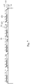
- FIG. 1 is a side view of a display device according to an embodiment of the present disclosure
- FIG. 2 is a side view of the white light-emitting unit shown in FIG. 1 ;
- FIG. 3 is a top view of the display device shown in FIG. 1 ;
- FIG. 4 is flow diagram of a method of manufacturing a display device according to an embodiment of the present disclosure.
- FIGS. 5-10 are cross-sectional views of a process at various stages of a method of manufacturing a display device according to an embodiment of the present disclosure.
- FIG. 1 is a side view of a display device 100 according to an embodiment of the present disclosure.
- FIG. 2 is a side view of the white light-emitting unit 120 shown in FIG. 1 .
- the display device 100 includes a substrate 110 , a plurality of white light-emitting units 120 , and a color filter layer 130 .
- the substrate 110 may be a substrate having conductive traces, such as a thin film transistor substrate, a glass substrate, a quartz substrate, or a silicon substrate, but the present disclosure is not limited in this regard.
- the white light-emitting units 120 are arranged on the substrate 110 at intervals, that is, gaps G are between the white light-emitting units 120 .
- the color filter layer 130 is disposed over the white light-emitting units 120 .
- each of the white light-emitting units 120 includes a light-emitting diode chip 122 and a wavelength conversion film 124 .
- the white light-emitting unit 120 is chip scale package (CSP), that is, the wavelength conversion film 124 directly covers a top surface 121 and side surfaces 123 of the light-emitting diode chip 122 .
- the light-emitting diode chip 122 is a light-emitting diode chip without substrate, for example, the light-emitting diode chip 122 has no sapphire substrate, such that an overall size of the white light-emitting unit 120 is reduced.
- a thickness H of the white light-emitting unit 120 including the light-emitting diode chip 122 without substrate is in a range from about 8 ⁇ m to about 110 ⁇ m, in which a thickness H 1 of the light-emitting diode chip 122 is in a range from about 5 ⁇ m to about 10 ⁇ m, and a thickness H 2 of the wavelength conversion film 124 is in a range from about 3 ⁇ m to about 100 ⁇ m. Since the white light-emitting unit 120 has a smaller size to be arranged in a high-density manner, the display device 100 is able to have a good uniformity of illumination.
- the light-emitting diode chip 122 includes an n-type semiconductor layer 122 a , a luminous layer 122 b , a p-type semiconductor layer 122 c , a protecting layer 122 d , a positive electrode 122 e , and a negative electrode 122 f .
- the luminous layer 122 b is between the n-type semiconductor layer 122 a and the p-type semiconductor layer 122 c , and the wavelength conversion film 124 covers a top surface 121 a and side surfaces 123 a of the n-type semiconductor layer 122 a , side surfaces 123 b of the luminous layer 122 b , and side surfaces 123 c of the p-type semiconductor layer 122 c .
- the n-type semiconductor layer 122 a is an n-type gallium nitride semiconductor layer
- the p-type semiconductor layer 122 c is a p-type gallium nitride semiconductor layer.
- a thickness H 3 of the n-type semiconductor layer 122 a is in a range from about 2.0 ⁇ m to about 3.5 ⁇ m, and a thickness H 5 of the p-type semiconductor layer 122 c is about 0.17 ⁇ m. Furthermore, a thickness H 4 of the luminous layer 122 b is in a range from about 0.05 ⁇ m to about 0.09 ⁇ m. Additionally, the positive electrode 122 e and the negative electrode 122 f may be made of a material including metal or alloy, but the present disclosure is not limited in this regard.
- the light-emitting diode chip 122 generates blue light
- the wavelength conversion film 124 converts the blue light generated by the light-emitting diode chip 122 into white light, such that the white light-emitting unit 120 can emit white light
- the wavelength conversion film 124 may include a plurality of first quantum dots 124 a and a plurality of second quantum dots 124 b .
- the first quantum dots 124 a convert the blue light generated by the light-emitting diode chip 122 into red light
- the second quantum dots 124 b convert the blue light generated by the light-emitting diode chip 122 into green light.
- each of the white-light emitting units 120 is a chip scale package (CSP), and each of the chip scale packages can emit white light.
- CSP chip scale package
- each of the white-light emitting units 120 can emit white light, electrical controlling problems can be avoided.
- the conventional display device includes a plurality of red, green, and blue light-emitting units, and since a voltage difference is between each of the light-emitting units, the electrical properties of the display device are not easily controlled.
- the display device 100 of the present disclosure directly includes a plurality of white light-emitting units 120 , such that the above-mentioned electrical controlling problems caused by the voltage difference are prevented.
- FIG. 3 is a top view of the display device 100 shown in FIG. 1 .
- the color filter layer 130 includes a plurality of color resists 132 , and each of the color resists 132 may be a red color resist 132 R, a green color resist 132 G, or a blue color resist 132 B.
- Each of the color resists 132 corresponds to a different white light-emitting unit 120 .
- each of the color resists 132 can convert the white light emitted by the corresponding white-light emitting unit 120 into light of a corresponding color, for example, red light, green light or blue light.
- the color resists 132 may be arranged in an array.
- the red color resist 132 R, the green color resist 132 G, and the blue color resist 132 B may be adjacently arranged to form a pixel unit.
- the arrangement of the color resists 132 is not limited in this regard, and may be determined as deemed necessary by designers.
- the color filter layer 130 further includes a black matrix 134 between the color resists 132 .
- the black matrix 134 has good light shielding properties to avoid light leakage between the color resists 132 or the pixel units, thereby improving the contrast presented by the display device 100 .
- the display device 100 obtain light of various colors through the combination of the white light-emitting units 120 and the color filter layer 130 , and each of the white-light emitting units 120 corresponds to one color resist 132 , distinct bright and dark areas are not easily produced regardless of the angle or manner in which the white light-emitting units 120 are arranged, thereby improving the uniformity of illumination of the display device 100 .
- the corresponding color light can be generated without affecting the color resolution by applying a high-resolution color filter layer 130 matching the different color resists 132 to the different white light-emitting units 120 .
- FIG. 4 is flow diagram of the method of manufacturing the display device 100 according to an embodiment of the present disclosure.
- the method of manufacturing the display device 100 includes the following steps.
- step S 10 a plurality of chip-scale packaged white light-emitting units are formed on a carrier.
- step S 20 any number of the white light-emitting units is transferred onto a substrate.
- step S 30 a color filter layer is disposed over the chip-scale packaged white light-emitting units.
- FIG. 5 is a cross-sectional view of a process at specific stages of the method of manufacturing the display device 100 according to an embodiment of the present disclosure.
- a substrate 150 e.g., a sapphire substrate
- the light-emitting diode chips 122 are arranged along an extending direction D of the substrate 150 , and gaps G 1 are between the light-emitting diode chips 122 .
- the light-emitting diode chips 122 with the substrate 150 are placed upside down and placed on a carrier 170 through an adhesive layer 160 .
- this step is to place the light-emitting diode chips 122 with the substrate 150 on the carrier 170 in a flip-chip manner.
- an n-type semiconductor layers 122 a of the light-emitting diode chips 122 are attached to the substrate 150 , and positive electrodes 122 e and negative electrodes 122 f of the light-emitting diode chips 122 are adhered to the carrier 170 through the adhesive layer 160 , such that the substrate 150 and the carrier 170 are located on opposite sides of the light-emitting diode chips 122 .
- FIG. 6 is a cross-sectional view of a process at specific stages of the method of manufacturing the display device 100 according to an embodiment of the present disclosure.
- the substrate 150 on the light-emitting diode chips 122 is subsequently removed.
- a plurality of light-emitting diode chips 122 without substrate are disposed on the carrier 170 .
- the substrate 150 can be removed through laser lift-off (LLO), but the present disclosure is not limited in this regard.
- LLO laser lift-off
- FIG. 7 is a cross-sectional view of a process at step S 10 of the method of manufacturing the display device 100 according to an embodiment of the present disclosure.
- the wavelength conversion films 124 are formed over the carrier 170 through lamination to cover the top surface 121 and the side surfaces 123 of each of the light-emitting diode chips 122 , such that the wavelength conversion films 124 and the light-emitting diode chips 122 have a same profile.
- the wavelength conversion films 124 are connected to each other between the light-emitting diode chips 122 , and the connected portions are adhered to the adhesive layer 160 .
- the wavelength conversion films 124 have a small thickness H 2 , the gaps G 1 between the adjacent light-emitting diode chips 122 are not filled with the wavelength conversion films 124 .
- the usage amount of material of the wavelength conversion films 124 can be reduced, thereby reducing the production cost and the overall size of the display device 100 .
- the wavelength conversion film 124 and the light-emitting diode chip 122 covered therein may be regarded as a chip-scale packaged white light-emitting unit 120 .
- a plurality of chip-scale packaged white light-emitting units 120 are disposed on the carrier 170 .
- FIG. 8 is a cross-sectional view of a process at step S 20 of the method of manufacturing the display device 100 according to an embodiment of the present disclosure.
- step S 20 any number of the white light-emitting units 120 on the carrier 170 is adsorbed, such that the wavelength conversion films 124 are disconnected from each other between the light-emitting diode chips 122 .
- the white light-emitting units 120 on the carrier 170 can be selectively adsorbed by transposition heads 180 (e.g., a poly(dimethyl siloxane) transposition head) through micro-transfer printing ( ⁇ TP).
- transposition heads 180 e.g., a poly(dimethyl siloxane) transposition head
- ⁇ TP micro-transfer printing
- the white light-emitting units 120 are adsorbed through the Van der Waals force between the transposition heads 180 and the wavelength conversion films 124 .
- FIG. 9 is a cross-sectional view of a process at step S 20 of the method of manufacturing the display device 100 according to an embodiment of the present disclosure.
- Step S 20 is continuously performed.
- the white light-emitting units 120 adsorbed to the transposition heads 180 are transferred to a corresponding position of the substrate 110 .
- the white light-emitting units 120 may be adhered to the substrate 110 by eutectic soldering.
- the white light-emitting units 120 may be adhered to the substrate 110 by solder paste reflowing.
- conductive features 190 can be formed to stick the white light-emitting units 120 to the substrate 110 .
- step S 20 the white light-emitting units 120 on the carrier 170 can be selectively adsorbed in accordance with the position on the substrate 110 where the white light-emitting units 120 are to be placed. In some embodiments, gaps G are between the white light-emitting units 120 .
- FIG. 10 is a cross-sectional view of a process at step S 30 of the method of manufacturing the display device 100 according to an embodiment of the present disclosure.
- the color filter layer 130 is disposed above the white light-emitting units 120 , and each of the color resists 132 of the color filter layer 130 is corresponded to a different white light-emitting unit 120 .
- the conductive features 190 are omitted in FIG. 10 for clarity.
- the white light-emitting units 120 including the wavelength conversion films 124 are directly disposed on the substrate 110 in step S 20 , there's no need for additionally providing other wavelength conversion layers between the color filter layer 130 and the white light-emitting units 120 , such that a distance D 1 between the color filter layer 130 and the white light-emitting units 120 is reduced, thereby reducing the overall size of the display device 100 .
- the wavelength conversion films directly cover the top surfaces and the side surfaces of the light-emitting diode chips to form the white light-emitting units with chip scale package, the overall thickness of the display device can be reduced.
- the white light-emitting units are matched with the color filter layer to obtain light of various colors, which can improve the uniformity of illumination of the display device and solve the problem of electrical controlling difficulties.
- the usage amount of the material of the wavelength conversion films can be reduced by directly disposing the chip-scale packaged white light-emitting units on the substrate, and hence reduces the production cost.
Landscapes
- Physics & Mathematics (AREA)
- General Physics & Mathematics (AREA)
- Engineering & Computer Science (AREA)
- Theoretical Computer Science (AREA)
- Led Device Packages (AREA)
Abstract
Description
Claims (7)
Priority Applications (2)
| Application Number | Priority Date | Filing Date | Title |
|---|---|---|---|
| US17/644,792 US12463077B2 (en) | 2019-10-31 | 2021-12-17 | Method of manufacturing display device |
| US19/377,021 US20260060035A1 (en) | 2019-10-31 | 2025-11-02 | Method of manufacturing display device |
Applications Claiming Priority (2)
| Application Number | Priority Date | Filing Date | Title |
|---|---|---|---|
| TW108139562A TW202119652A (en) | 2019-10-31 | 2019-10-31 | Display device and manufacturing method thereof |
| TW108139562 | 2019-10-31 |
Related Child Applications (1)
| Application Number | Title | Priority Date | Filing Date |
|---|---|---|---|
| US17/644,792 Continuation-In-Part US12463077B2 (en) | 2019-10-31 | 2021-12-17 | Method of manufacturing display device |
Publications (2)
| Publication Number | Publication Date |
|---|---|
| US20210135063A1 US20210135063A1 (en) | 2021-05-06 |
| US11469352B2 true US11469352B2 (en) | 2022-10-11 |
Family
ID=75645112
Family Applications (1)
| Application Number | Title | Priority Date | Filing Date |
|---|---|---|---|
| US16/698,980 Active 2040-01-27 US11469352B2 (en) | 2019-10-31 | 2019-11-28 | Display device and manufacturing method thereof |
Country Status (3)
| Country | Link |
|---|---|
| US (1) | US11469352B2 (en) |
| CN (1) | CN112750852B (en) |
| TW (1) | TW202119652A (en) |
Families Citing this family (4)
| Publication number | Priority date | Publication date | Assignee | Title |
|---|---|---|---|---|
| TW202119652A (en) | 2019-10-31 | 2021-05-16 | 隆達電子股份有限公司 | Display device and manufacturing method thereof |
| US12463077B2 (en) | 2019-10-31 | 2025-11-04 | Lextar Electronics Corporation | Method of manufacturing display device |
| TWI810725B (en) * | 2021-11-26 | 2023-08-01 | 鴻海精密工業股份有限公司 | Display panel and method for driving same |
| CN116189610A (en) | 2021-11-26 | 2023-05-30 | 鸿海精密工业股份有限公司 | Display panel and driving method thereof |
Citations (9)
| Publication number | Priority date | Publication date | Assignee | Title |
|---|---|---|---|---|
| KR20110111090A (en) | 2010-04-02 | 2011-10-10 | 엘지이노텍 주식회사 | Light emitting diode lens and liquid crystal display device including the same |
| US20140339495A1 (en) | 2013-05-14 | 2014-11-20 | LuxVue Technology Corporation | Micro led with wavelength conversion layer |
| US20170054053A1 (en) | 2015-08-21 | 2017-02-23 | Lg Electronics Inc. | Light emitting device package assembly and method of fabricating the same |
| US20170133357A1 (en) | 2015-11-05 | 2017-05-11 | Innolux Corporation | Display device |
| US20180190871A1 (en) | 2015-06-19 | 2018-07-05 | Seoul Viosys Co., Ltd. | Light-emitting element comprising a plurality of wavelength converters, and production method therefor |
| CN110024484A (en) | 2016-11-25 | 2019-07-16 | Lg电子株式会社 | Display device using semiconductor light-emitting device and method of manufacturing the same |
| US20190378873A1 (en) * | 2016-11-24 | 2019-12-12 | Lg Innotek Co., Ltd. | Semiconductor device and display device comprising same |
| US20200144460A1 (en) * | 2017-07-03 | 2020-05-07 | Sharp Kabushiki Kaisha | Light source device and light emitting device |
| TW202119652A (en) | 2019-10-31 | 2021-05-16 | 隆達電子股份有限公司 | Display device and manufacturing method thereof |
Family Cites Families (19)
| Publication number | Priority date | Publication date | Assignee | Title |
|---|---|---|---|---|
| US20040061810A1 (en) * | 2002-09-27 | 2004-04-01 | Lumileds Lighting, U.S., Llc | Backlight for a color LCD using wavelength-converted light emitting devices |
| KR20120063815A (en) * | 2010-12-08 | 2012-06-18 | 삼성엘이디 주식회사 | Light emitting diode package and manufaturing method thereof |
| US8957429B2 (en) * | 2012-02-07 | 2015-02-17 | Epistar Corporation | Light emitting diode with wavelength conversion layer |
| KR102043322B1 (en) * | 2013-02-12 | 2019-11-12 | 삼성디스플레이 주식회사 | Light emitting diode, display device including the same and method of manufacturing display device |
| KR20140133765A (en) * | 2013-05-09 | 2014-11-20 | 서울반도체 주식회사 | Light source module and backlight unit having the same |
| KR102144993B1 (en) * | 2013-10-02 | 2020-08-14 | 삼성전자주식회사 | Display device |
| CN204348757U (en) * | 2014-12-11 | 2015-05-20 | 北京中科天顺信息技术有限公司 | Fluorescence switch plant growth lamp unit, plant growth lamp components and plant growth lamp |
| KR101621820B1 (en) * | 2014-12-29 | 2016-05-17 | 삼성전자 주식회사 | Light source, back light unit and liquid crystal display including the light source |
| CN106531759B (en) * | 2015-09-09 | 2019-07-09 | 群创光电股份有限公司 | Display device |
| JP2017157724A (en) * | 2016-03-02 | 2017-09-07 | デクセリアルズ株式会社 | Display device and manufacturing method thereof, and light emitting device and manufacturing method thereof |
| CN106098697B (en) * | 2016-06-15 | 2019-04-02 | 深圳市华星光电技术有限公司 | Micro light-emitting diode display panel and manufacturing method thereof |
| CN106684109B (en) * | 2017-01-04 | 2020-04-28 | 京东方科技集团股份有限公司 | Light-emitting diode display panel and its manufacturing method, display |
| WO2018169243A1 (en) * | 2017-03-13 | 2018-09-20 | 서울반도체주식회사 | Method for manufacturing display device |
| CN107452851A (en) * | 2017-05-25 | 2017-12-08 | 凃中勇 | Light emitting diode packaging assembly and multiple color temperature lighting device |
| US10749086B2 (en) * | 2017-07-21 | 2020-08-18 | Maven Optronics Co., Ltd. | Asymmetrically shaped light-emitting device, backlight module using the same, and method for manufacturing the same |
| CN108962882A (en) * | 2018-07-04 | 2018-12-07 | 深圳世元吉科技发展有限公司 | A kind of UV LED encapsulating structure, production method and sterilizing unit |
| CN109103344A (en) * | 2018-07-25 | 2018-12-28 | 云谷(固安)科技有限公司 | A kind of white light OLED device and display device |
| CN110085618B (en) * | 2019-03-29 | 2021-06-08 | 成都辰显光电有限公司 | Display panel preparation method |
| CN110265531B (en) * | 2019-06-14 | 2021-02-26 | 深圳市华星光电半导体显示技术有限公司 | Micro LEDs and Display Panels |
-
2019
- 2019-10-31 TW TW108139562A patent/TW202119652A/en unknown
- 2019-11-08 CN CN201911089495.9A patent/CN112750852B/en active Active
- 2019-11-28 US US16/698,980 patent/US11469352B2/en active Active
Patent Citations (10)
| Publication number | Priority date | Publication date | Assignee | Title |
|---|---|---|---|---|
| KR20110111090A (en) | 2010-04-02 | 2011-10-10 | 엘지이노텍 주식회사 | Light emitting diode lens and liquid crystal display device including the same |
| US20140339495A1 (en) | 2013-05-14 | 2014-11-20 | LuxVue Technology Corporation | Micro led with wavelength conversion layer |
| US20180190871A1 (en) | 2015-06-19 | 2018-07-05 | Seoul Viosys Co., Ltd. | Light-emitting element comprising a plurality of wavelength converters, and production method therefor |
| US20170054053A1 (en) | 2015-08-21 | 2017-02-23 | Lg Electronics Inc. | Light emitting device package assembly and method of fabricating the same |
| US20170133357A1 (en) | 2015-11-05 | 2017-05-11 | Innolux Corporation | Display device |
| US20190237452A1 (en) * | 2015-11-05 | 2019-08-01 | Innolux Corporation | Display device having a plurality of bank structures |
| US20190378873A1 (en) * | 2016-11-24 | 2019-12-12 | Lg Innotek Co., Ltd. | Semiconductor device and display device comprising same |
| CN110024484A (en) | 2016-11-25 | 2019-07-16 | Lg电子株式会社 | Display device using semiconductor light-emitting device and method of manufacturing the same |
| US20200144460A1 (en) * | 2017-07-03 | 2020-05-07 | Sharp Kabushiki Kaisha | Light source device and light emitting device |
| TW202119652A (en) | 2019-10-31 | 2021-05-16 | 隆達電子股份有限公司 | Display device and manufacturing method thereof |
Non-Patent Citations (1)
| Title |
|---|
| "[High-industry research and analysis] Micro LED mass transfer technology route analysis", http://read01.com/yyODJMd.html#.YWjaTBpBxhE, Advanced Industry Research Institute, Feb. 6, 2019. |
Also Published As
| Publication number | Publication date |
|---|---|
| CN112750852A (en) | 2021-05-04 |
| TW202119652A (en) | 2021-05-16 |
| CN112750852B (en) | 2024-10-18 |
| US20210135063A1 (en) | 2021-05-06 |
Similar Documents
| Publication | Publication Date | Title |
|---|---|---|
| US12368145B2 (en) | Display apparatus and manufacturing method thereof | |
| US11469352B2 (en) | Display device and manufacturing method thereof | |
| US10886257B2 (en) | Micro LED display device and method for manufacturing same | |
| US10096647B2 (en) | Display apparatus having a plurality of reflective electrodes | |
| EP3439042B1 (en) | Display device and manufacturing method therefor | |
| US11233185B2 (en) | Display device and method of fabricating the same | |
| US9831387B2 (en) | Light engine array | |
| KR20130137985A (en) | Display device using semiconductor light emitting device | |
| TWI811680B (en) | Light-emitting diode micro display device | |
| KR102927912B1 (en) | Display device | |
| CN114762122A (en) | LED display device | |
| US10229896B2 (en) | Light emitting diode apparatus and method for manufacturing the same | |
| US12463077B2 (en) | Method of manufacturing display device | |
| Zeng et al. | Optical crosstalk among mini-LEDs packaged in a four-in-one integrated matrix device | |
| KR102900223B1 (en) | Micro led and display module having the same | |
| JP7507036B2 (en) | Display device | |
| US12575236B2 (en) | Pixel module and display apparatus having the same | |
| US12237458B2 (en) | Micro light emitting device display apparatus | |
| TWI781029B (en) | Display device and manufacturing method thereof | |
| US20230068483A1 (en) | Micro led display device | |
| US20250031498A1 (en) | Display Panel and Display Apparatus Including Same | |
| WO2023228918A1 (en) | Light-emitting device and method for producing light-emitting device | |
| CN118176582A (en) | Display module and method of manufacturing the same | |
| KR20240077614A (en) | Appratus for fabricating display panel | |
| CN119914841A (en) | Light source module |
Legal Events
| Date | Code | Title | Description |
|---|---|---|---|
| AS | Assignment |
Owner name: LEXTAR ELECTRONICS CORPORATION, TAIWAN Free format text: ASSIGNMENT OF ASSIGNORS INTEREST;ASSIGNORS:CHEN, FU-HSIN;LEE, YU-CHUN;TONG, HUNG-CHUN;AND OTHERS;SIGNING DATES FROM 20191113 TO 20191115;REEL/FRAME:051136/0961 |
|
| FEPP | Fee payment procedure |
Free format text: ENTITY STATUS SET TO UNDISCOUNTED (ORIGINAL EVENT CODE: BIG.); ENTITY STATUS OF PATENT OWNER: LARGE ENTITY |
|
| STPP | Information on status: patent application and granting procedure in general |
Free format text: NON FINAL ACTION MAILED |
|
| STPP | Information on status: patent application and granting procedure in general |
Free format text: RESPONSE TO NON-FINAL OFFICE ACTION ENTERED AND FORWARDED TO EXAMINER |
|
| STPP | Information on status: patent application and granting procedure in general |
Free format text: NOTICE OF ALLOWANCE MAILED -- APPLICATION RECEIVED IN OFFICE OF PUBLICATIONS |
|
| STPP | Information on status: patent application and granting procedure in general |
Free format text: AWAITING TC RESP, ISSUE FEE PAYMENT RECEIVED |
|
| STPP | Information on status: patent application and granting procedure in general |
Free format text: AWAITING TC RESP, ISSUE FEE PAYMENT VERIFIED |
|
| STPP | Information on status: patent application and granting procedure in general |
Free format text: RESPONSE TO NON-FINAL OFFICE ACTION ENTERED AND FORWARDED TO EXAMINER |
|
| STPP | Information on status: patent application and granting procedure in general |
Free format text: FINAL REJECTION MAILED |
|
| STPP | Information on status: patent application and granting procedure in general |
Free format text: DOCKETED NEW CASE - READY FOR EXAMINATION |
|
| STPP | Information on status: patent application and granting procedure in general |
Free format text: NOTICE OF ALLOWANCE MAILED -- APPLICATION RECEIVED IN OFFICE OF PUBLICATIONS |
|
| STPP | Information on status: patent application and granting procedure in general |
Free format text: PUBLICATIONS -- ISSUE FEE PAYMENT VERIFIED |
|
| STCF | Information on status: patent grant |
Free format text: PATENTED CASE |
|
| MAFP | Maintenance fee payment |
Free format text: PAYMENT OF MAINTENANCE FEE, 4TH YEAR, LARGE ENTITY (ORIGINAL EVENT CODE: M1551); ENTITY STATUS OF PATENT OWNER: LARGE ENTITY Year of fee payment: 4 |