US11460952B2 - Apparatus and method for automatically calibrating capacitance per channel - Google Patents
Apparatus and method for automatically calibrating capacitance per channel Download PDFInfo
- Publication number
- US11460952B2 US11460952B2 US16/840,833 US202016840833A US11460952B2 US 11460952 B2 US11460952 B2 US 11460952B2 US 202016840833 A US202016840833 A US 202016840833A US 11460952 B2 US11460952 B2 US 11460952B2
- Authority
- US
- United States
- Prior art keywords
- capacitance
- channel
- calibration
- parasitic
- parasitic capacitance
- Prior art date
- Legal status (The legal status is an assumption and is not a legal conclusion. Google has not performed a legal analysis and makes no representation as to the accuracy of the status listed.)
- Active, expires
Links
Images


Classifications
-
- G—PHYSICS
- G06—COMPUTING; CALCULATING OR COUNTING
- G06F—ELECTRIC DIGITAL DATA PROCESSING
- G06F3/00—Input arrangements for transferring data to be processed into a form capable of being handled by the computer; Output arrangements for transferring data from processing unit to output unit, e.g. interface arrangements
- G06F3/01—Input arrangements or combined input and output arrangements for interaction between user and computer
- G06F3/03—Arrangements for converting the position or the displacement of a member into a coded form
- G06F3/041—Digitisers, e.g. for touch screens or touch pads, characterised by the transducing means
- G06F3/0416—Control or interface arrangements specially adapted for digitisers
- G06F3/0418—Control or interface arrangements specially adapted for digitisers for error correction or compensation, e.g. based on parallax, calibration or alignment
-
- G—PHYSICS
- G01—MEASURING; TESTING
- G01R—MEASURING ELECTRIC VARIABLES; MEASURING MAGNETIC VARIABLES
- G01R27/00—Arrangements for measuring resistance, reactance, impedance, or electric characteristics derived therefrom
- G01R27/02—Measuring real or complex resistance, reactance, impedance, or other two-pole characteristics derived therefrom, e.g. time constant
- G01R27/26—Measuring inductance or capacitance; Measuring quality factor, e.g. by using the resonance method; Measuring loss factor; Measuring dielectric constants ; Measuring impedance or related variables
- G01R27/2605—Measuring capacitance
-
- G—PHYSICS
- G06—COMPUTING; CALCULATING OR COUNTING
- G06F—ELECTRIC DIGITAL DATA PROCESSING
- G06F3/00—Input arrangements for transferring data to be processed into a form capable of being handled by the computer; Output arrangements for transferring data from processing unit to output unit, e.g. interface arrangements
- G06F3/01—Input arrangements or combined input and output arrangements for interaction between user and computer
- G06F3/03—Arrangements for converting the position or the displacement of a member into a coded form
- G06F3/041—Digitisers, e.g. for touch screens or touch pads, characterised by the transducing means
- G06F3/044—Digitisers, e.g. for touch screens or touch pads, characterised by the transducing means by capacitive means
- G06F3/0447—Position sensing using the local deformation of sensor cells
-
- H—ELECTRICITY
- H03—ELECTRONIC CIRCUITRY
- H03K—PULSE TECHNIQUE
- H03K17/00—Electronic switching or gating, i.e. not by contact-making and –breaking
- H03K17/94—Electronic switching or gating, i.e. not by contact-making and –breaking characterised by the way in which the control signals are generated
- H03K17/96—Touch switches
- H03K17/962—Capacitive touch switches
Definitions
- the present disclosure relates to an apparatus and method for automatically calibrating capacitance per channel, and more particularly, to an apparatus and method for automatically calibrating capacitance per channel, for measuring parasitic capacitance values of respective channels due to a difference in a length of a wiring of each capacitance sensing channel when a circuit is designed and adding a unique calibration capacitance value of each channel such that all channels have the same reference capacitance value that is preset.
- FIG. 1 is a diagram for explaining formation of a parasitic capacitance depending on a length of a wiring for each capacitance sensing channel.
- a printed circuit board (PCB)
- channels are connected through wirings (trace or route) according to arrangement of touch sensor integrated circuits (ICs) and touch electrodes.
- the length of a wiring connected to the touch electrode from the touch sensor IC is changed according to arrangement of touch electrodes. That is, as shown in the drawing, arrangement positions of capacitance sensing patterns KEY1 and KEY2 on the PCB are inevitably designed with different distances from a touch sensor IC chip.
- a capacitance value with a surrounding ground (GND) pattern is formed in an electric wiring (trace or route), which is referred to as a parasitic capacitance C p .
- the touch electrodes may be a copper film pattern on the PCB and may also be assembled using a separate conductive device (metal gasket or spring pin).
- an entire parasitic capacitance (C) value based on a channel pin having the shortest wiring length is lowest (CS 0 and KEY0), and an entire parasitic capacitance value based on a channel pin having the longest wiring length is highest (CS 2 and KEY2).
- FIG. 2 is a diagram for explaining a value of sensitivity of a conventional capacitance sensing touch sensor.
- FIGS. 2A and 2B show a digital change value (delta or difference data) related to sensitivity measured by a touch sensor IC.
- FIG. 2A is a graph showing a value that is measured using touch sticks with a diameter of 5 mm, 8 mm, and 10 mm, which are sequentially used, over time with respect to a corresponding channel, and it may be seen that the sensitivity of a channel CS 0 (KEY0) with the lowest parasite C is measured to be higher than other channels.
- a ratio of sensitivity to a predetermined C value change may be changed depending on different parasitic capacitance (C) values for respective channels in a conventional touch sensor IC.
- the smallest parasite C value may be formed, the highest sensitivity value may be formed during touch.
- the largest parasite C value may be formed, and the lowest sensitivity value may be formed during touch. This is because a ratio of variation of capacitance formed in an electrode CS 0 by a touch stick to an originally formed parasite C value (total C P_CS0 ) is higher than other channels CS 1 and CS 2 .
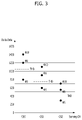
- FIG. 3 is a diagram for explaining setting of a threshold (THD) level based on the sensitivity of a conventional capacitance sensing touch sensor.
- TDD threshold
- a ratio of sensitivity to a predetermined C value change (finger capacitance (CF)) during an external touch is entirely changed depending on a parasite C value that is different for each channel in a conventional touch sensor IC.
- a threshold level is required.
- a target object needs not to be touched under a condition of a touch stick with a diameter of 5 ⁇ and needs to be pressed under a condition of a touch stick with a diameter of 10 ⁇ .
- a THD level may be formed at a diameter of about 7 ⁇ .
- a sensitivity value level of each channel is different, and thus, a THD level for each channel is differently set. This causes serious inconvenience because a sensitivity value needs to be checked and set for each channel during development related to sensitivity tuning.
- the present disclosure is directed to an apparatus and method for automatically calibrating capacitance per channel, for automatically calibrating a capacitance value of each channel to a preset reference capacitance value in order to simplify a sensitivity tuning development procedure due to a difference in a parasitic capacitance value due to a difference in a length of a wiring of each capacitance sensing channel when a circuit is designed.
- an apparatus for automatically calibrating a capacitance per channel includes a touch sensing device including a plurality of touch sensing regions, and a capacitance measurement and calibration device configured to measure parasitic capacitances of channels connected to the plurality of touch sensing regions, respectively, and to add a unique calibration capacitance of each channel to a corresponding channel to acquire a preset reference capacitance when each channel is connected to the parasitic capacitance.
- the capacitance measurement and calibration device may be connected in parallel to the parasitic capacitance.
- the capacitance measurement and calibration device may include a calibration controller configured to measure a parasitic capacitance of each channel, to compare the measured parasitic capacitance of each channel with the reference capacitance, and to generate a calibration control signal for each channel corresponding to a comparison result, and a capacitance calibration circuit including a plurality of capacitance calibration modules configured to add calibration capacitances for respective corresponding channels to the respective channels in response to the calibration control signal for each channel.
- a method of automatically calibrating a capacitance per channel performed by the apparatus for automatically calibrating capacitance per channel includes measuring a parasitic capacitance per channel, for measuring the parasitic capacitance for each channel of the touch sensing device, detecting a maximum parasitic capacitance, for detecting a largest parasitic capacitance of the measured parasitic capacitances for respective channels, generating a calibration control signal, for comparing the maximum parasitic capacitance with the parasitic capacitance of each channel and generating a calibration control signal for each channel in response to a difference in capacitance, and adding a calibration capacitance, for adding each calibration capacitance to a corresponding channel in response to a corresponding control signal of the calibration control signal, wherein the measuring the parasitic capacitance per channel, the detecting the maximum parasitic capacitance, and the generating the calibration control signal are performed by the capacitance measurement and calibration device, and wherein the adding the calibration capacitance is performed by the plurality of capacitance calibration modules.
- a method performed by the apparatus for automatically calibrating capacitance per channel includes measuring a parasitic capacitance per channel, for measuring the parasitic capacitance for each channel of the touch sensing device, detecting a maximum parasitic capacitance, for detecting a largest parasitic capacitance of the measured parasitic capacitances for respective channels, generating a calibration control signal, for comparing the maximum parasitic capacitance with the parasitic capacitance of each channel and generating a calibration control signal for each channel in response to a difference in capacitance, and adding a calibration capacitance, for adding each calibration capacitance to a corresponding channel in response to a corresponding control signal of the calibration control signal, wherein the measuring the parasitic capacitance per channel, the detecting the maximum parasitic capacitance, and the generating the calibration control signal are performed by the capacitance measurement and calibration device, and wherein the adding the calibration capacitance is performed by the plurality of capacitance calibration modules.
- FIG. 1 is a diagram for explaining formation of a parasitic capacitance depending on a length of a wiring for each capacitance sensing channel;
- FIGS. 2A and 2B are diagrams for explaining a value of sensitivity of a conventional capacitance sensing touch sensor
- FIG. 3 is a diagram for explaining setting of a threshold (THD) level based on the sensitivity of a conventional capacitance sensing touch sensor;
- FIG. 4 is a diagram showing a concept of an apparatus for automatically calibrating a capacitance per channel according to an embodiment of the present disclosure
- FIG. 5 is a diagram showing a concept of auto-calibration of a channel capacitance C according to an embodiment of the present disclosure
- FIGS. 6A and 6B are diagrams for explaining setting of a threshold (THD) level according to the present disclosure
- FIG. 7 is a diagram showing a configuration of a method of automatically calibrating a capacitance per channel according to an embodiment of the present disclosure
- FIG. 8 is a diagram for explaining an algorithm of a method of automatically calibrating a capacitance according to an embodiment of the present disclosure.
- FIG. 9 is a diagram showing a configuration of a method of automatically calibrating a capacitance per channel according to another embodiment of the present disclosure.
- FIG. 4 is a diagram showing a concept of an apparatus for automatically calibrating a capacitance per channel according to an embodiment of the present disclosure.
- FIG. 5 is a diagram showing a concept of auto-calibration of a channel capacitance C according to an embodiment of the present disclosure.
- the apparatus for automatically calibrating a capacitance per channel may include a touch sensing device 10 and a capacitance measurement and calibration device 20 , in which case basic connection and configuration states may be understood with reference to FIG. 1 together.
- the touch sensing device 10 may include a plurality of touch sensing regions. That is, the touch sensing device 10 may include a plurality of touch electrodes 11 , i.e., (N+1) touch electrodes 11 to ‘KEY N’ from ‘KEY 0 ’.
- the touch electrodes 11 may be formed as a copper film pattern on a printed circuit board (PCB) and may also be assembled using a separate conductive device such as a metal gasket or a spring pin. Positions of the touch electrodes 11 that correspond to a capacitance sensing pattern may has the same distance or different distances from the capacitance measurement and calibration device 20 . Thus, referring to FIG.
- parasitic capacitances C p_CS0 , C p_CS1 , and C p_CS2 may be inevitably different depending on the length of a wiring, and it may be seen that a parasitic capacitance of the touch electrode 11 that is farthest from the capacitance measurement and calibration device 20 is highest.
- the capacitance measurement and calibration device 20 may measure parasitic capacitances of channels that are connected to the plurality of touch electrodes 11 , respectively, and may add a unique calibration capacitance of each channel to a corresponding channel and may equalize the capacitances of the channels to acquire a preset reference capacitance when each channel is connected to the parasitic capacitance.
- the reference capacitance may be a maximum value, a minimum value, or a preset different value.
- the capacitance measurement and calibration device 20 may include a calibration controller 21 and a capacitance calibration circuit 22 .
- the calibration controller 21 may be connected to each of the touch electrodes 11 and may measure a parasitic capacitance of each connected channel.
- the calibration controller 21 may compare the reference capacitance with the measured parasitic capacitance of each channel. After comparison, a calibration control signal S 1 for each channel corresponding to the comparison result may be generated.
- the calibration control signal S 1 may be, for example, a control command for automatically calibrating capacitance values of different channels based on a channel reference value formed with the largest value to acquire the same value.
- the capacitance calibration circuit 22 may include a plurality of capacitance calibration modules for adding calibration capacitances for respective corresponding channels to the respective channels in response to the calibration control signal S 1 for each channel.
- a touch sensor IC that is the capacitance measurement and calibration device 20 may read all capacitance (C) values formed in respective channels and may calibrate internal capacitance values for the respective channels. That is, calibration capacitances for respective channels may be added to respective channels through the capacitance calibration circuit 22 according to the calibration control signal S 1 , and in this regard, based on a channel capacitance reference value formed with the largest value, capacitance values of other channels may be automatically calibrated. For example, all capacitance values may be equalized to 20 pF by calibrating CS 0 to add 16p F and calibrating CS 1 to add 10 pF based on 20 pF that is an entire capacitance value of CS 2 .
- the capacitance measurement and calibration device 20 may be connected in parallel to the parasitic capacitance. That is, the capacitance calibration module may be configured as a circuit including a plurality of capacitors that are each connected in parallel to the parasitic capacitance. For example, referring to FIG. 5 , parasitic capacitances ‘C p_CS0 ’, ‘C p_CS1 ’, and ‘C p_CS2 ’ may each be connected in parallel to 20 capacitors, an on/off switch may be connected to each capacitor, and each capacitor may have a capacitance of 1 pF.
- the on/off switch may be operated according to the calibration control signal S 1 , and with regard to the capacitors that are connected in parallel to each other, capacitance values of the connected capacitors may be summed.
- a parasitic capacitance value of 4 pF and a calibration capacitance value of 16 pF may be summed to automatically calibrate ‘CS 0 ’ to 20 pF while 16 on/off switches are connected.
- ‘CS 1 ’ may be automatically calibrated to 20 pF while 10 on/off switches are connected, and ‘CS 2 ’ may be maintained without connected switch.
- a capacitor that is connected in parallel to a parasitic capacitance may be configured to have a decimal point but not an integer, for example, 1.1, 1.2, 1.3, . . . to enable more precious calibration.
- FIG. 6 is a diagram for explaining setting of a threshold (THD) level according to the present disclosure.
- FIG. 6A shows sensitivity values for respective channels CS 0 , CS 1 , and CS 2 using a touch stick with a diameter of 5 ⁇ , 8 ⁇ , and 10 ⁇ and differently set THD levels for the respective channels in a conventional configuration illustrated in FIG. 1 .
- This causes serious inconvenience because a sensitivity value needs to be checked and set for each channel during development related to sensitivity tuning.
- FIG. 6B shows sensitivity values and THD levels that are measured through auto-calibration related to a C value of a touch sensor IC according to the present disclosure, and the configuration of FIG. 1 is applied without changes.
- the channels CS 0 , CS 1 , and CS 2 may have the same capacitance value through a capacitance value automatic calibration function, and thus, THD Levels may be managed as one level, as shown in FIG. 6B .
- THD Levels may be managed as one level, as shown in FIG. 6B .
- operations related thereto may also be easily performed.
- FIG. 7 is a diagram showing a configuration of a method of automatically calibrating a capacitance per channel according to an embodiment of the present disclosure.
- FIG. 8 is a diagram for explaining an algorithm of a method of automatically calibrating a capacitance according to an embodiment of the present disclosure. Basic configurations and states are understood with reference to the description of FIGS. 1 and 4 to 6 together.
- the method of automatically calibrating a capacitance per channel may be performed using the aforementioned apparatus for automatically calibrating capacitance per channel and may include measuring a parasitic capacitance per channel (S 10 ), detecting a maximum parasitic capacitance (S 20 ), generating a calibration control signal (S 30 ), and adding a calibration capacitance (S 40 ).
- the capacitance measurement and calibration device 20 may measure a parasitic capacitance of each channel of the touch sensing device 10 .
- the capacitance measurement and calibration device 20 may detect the largest parasitic capacitance of the measured parasitic capacitances for respective channels.
- the capacitance measurement and calibration device 20 may compare the maximum parasitic capacitance with the parasitic capacitance per channel and generate the calibration control signal S 1 for each channel in response to a difference in the capacitance.
- a plurality of calibration modules may add each calibration capacitance to a corresponding channel in response to a corresponding control signal of the calibration control signal S 1 , and the adding the calibration capacitance (S 40 ) may be performed by the aforementioned plurality of capacitance calibration modules.
- FIG. 8 The algorithm of a method of automatically calibrating a capacitance per channel according to an embodiment is illustrated in FIG. 8 , and referring to FIG. 8 , a first touch sensing channel may be checked. Parasite parasitic capacitance values of respective sensed channels may be measured. A channel of the largest parasitic capacitance value among the measured parasitic capacitance values may be recognized. Then, like in the description of FIG. 5 , capacitance values of all touch sensing channels may be adjusted to the largest parasitic capacitance value and then a THD level may be set based on the adjusted value and touch sensing may be performed as shown in FIG. 6B .
- FIG. 9 is a diagram showing a configuration of a method of automatically calibrating a capacitance per channel according to another embodiment of the present disclosure, and the present embodiment will be described with reference to the drawing.
- the method of automatically calibrating a capacitance per channel may be performed by the aforementioned apparatus for automatically calibrating capacitance per channel and may include measuring a parasitic capacitance per channel (S 10 ), generating a calibration control signal (S 30 ), and adding a calibration capacitance (S 40 ).
- the capacitance measurement and calibration device 20 may measure a parasitic capacitance of each channel of the touch sensing device 10 .
- the capacitance measurement and calibration device 20 may compare the measured parasitic capacitance of each channel with a preset reference capacitance and may generate the calibration control signal S 1 for each channel in response to a difference in the capacitance.
- a plurality of calibration modules may add each calibration capacitance to a corresponding channel in response to a corresponding control signal of the calibration control signal S 1 , and the adding the calibration capacitance (S 40 ) may be performed by the aforementioned plurality of capacitance calibration modules.
- a preset reference capacitance value may be used instead of the largest parasitic capacitance value as a reference.
- the reference capacitance value may be a minimum value or may be another capacitance values that is set depending on an operation environment.
- all channels may have the same capacitance value by automatically calibrating capacitance values for respective channels irrespective of a difference in parasitic capacitance values depending on a length of a wiring between channels, and thus, as well as a THD level setting operation, operations related thereto may also be easily performed.
- the aforementioned apparatus and method for automatically calibrating capacitance per channel according to the present disclosure may have the following effects.
- Parasite Parasitic capacitances of respective channels connected to a plurality of touch sensing regions may be measured, and a C value-related auto-calibration function of adding a unique calibration capacitance of each channel to a corresponding channel to acquire a preset reference capacitance when each channel is connected to the parasitic capacitance may be used, and thus, the same sensitivity value may be formed for the channels irrespective of touch sensors having wirings with different lengths and the same single THD level is set.
- a procedure of developing sensitivity tuning may be simplified, sensitivity tuning may be easily developed, and a development period thereof may be reduced.
Landscapes
- Engineering & Computer Science (AREA)
- General Engineering & Computer Science (AREA)
- Theoretical Computer Science (AREA)
- Physics & Mathematics (AREA)
- General Physics & Mathematics (AREA)
- Human Computer Interaction (AREA)
- Electronic Switches (AREA)
- Measurement Of Resistance Or Impedance (AREA)
- Investigating Or Analyzing Materials By The Use Of Electric Means (AREA)
Applications Claiming Priority (2)
| Application Number | Priority Date | Filing Date | Title |
|---|---|---|---|
| KR1020190059827A KR102302879B1 (ko) | 2019-05-22 | 2019-05-22 | 채널별 정전용량 자동 보정 장치 및 방법 |
| KR10-2019-0059827 | 2019-05-22 |
Publications (2)
| Publication Number | Publication Date |
|---|---|
| US20200371144A1 US20200371144A1 (en) | 2020-11-26 |
| US11460952B2 true US11460952B2 (en) | 2022-10-04 |
Family
ID=70277215
Family Applications (1)
| Application Number | Title | Priority Date | Filing Date |
|---|---|---|---|
| US16/840,833 Active 2041-02-17 US11460952B2 (en) | 2019-05-22 | 2020-04-06 | Apparatus and method for automatically calibrating capacitance per channel |
Country Status (4)
| Country | Link |
|---|---|
| US (1) | US11460952B2 (ko) |
| EP (1) | EP3742266B1 (ko) |
| KR (1) | KR102302879B1 (ko) |
| CN (1) | CN111984143A (ko) |
Families Citing this family (3)
| Publication number | Priority date | Publication date | Assignee | Title |
|---|---|---|---|---|
| CN112649777B (zh) * | 2020-11-27 | 2022-12-16 | 杨新芳 | 一种动态校准方法、设备及计算机可读存储介质 |
| WO2022170590A1 (zh) * | 2021-02-10 | 2022-08-18 | 深圳市汇顶科技股份有限公司 | 一种确定电容基准的方法、电容基准的确定装置和设备 |
| CN115328338A (zh) * | 2021-05-10 | 2022-11-11 | 法雷奥汽车内部控制(深圳)有限公司 | 用于方向盘触摸检测的方法和装置 |
Citations (8)
| Publication number | Priority date | Publication date | Assignee | Title |
|---|---|---|---|---|
| US20090153152A1 (en) | 2007-12-14 | 2009-06-18 | Cypress Semiconductor Corporation | Compensation circuit for a tx-rx capacitive sensor |
| KR100974637B1 (ko) | 2008-04-07 | 2010-08-06 | 서울대학교산학협력단 | 정전용량 검출 장치 및 이를 포함하는 정전용량 센서 |
| KR20110091380A (ko) | 2010-02-05 | 2011-08-11 | 삼성전자주식회사 | 터치 패널의 노이즈 보상 방법 및 장치 |
| KR20140141111A (ko) | 2013-05-31 | 2014-12-10 | 엘지디스플레이 주식회사 | 터치 스크린 구동 장치 |
| US9019220B1 (en) | 2012-03-14 | 2015-04-28 | Cypress Semiconductor Corporation | Baseline charge compensation |
| US20180173366A1 (en) | 2016-05-30 | 2018-06-21 | Boe Technology Group Co., Ltd. | Apparatus and method for capacitance calibration, and touch display screen |
| WO2018157595A1 (zh) | 2017-03-02 | 2018-09-07 | 京东方科技集团股份有限公司 | 触摸屏频点校准装置及方法、触摸屏和显示装置 |
| US10719182B2 (en) * | 2018-02-27 | 2020-07-21 | Kabushiki Kaisha Tokai Rika Denki Seisakusho | Touch sensor device and capacitance calibration method |
Family Cites Families (10)
| Publication number | Priority date | Publication date | Assignee | Title |
|---|---|---|---|---|
| US7777501B2 (en) | 2005-06-03 | 2010-08-17 | Synaptics Incorporated | Methods and systems for sigma delta capacitance measuring using shared component |
| KR20110112128A (ko) * | 2010-04-06 | 2011-10-12 | 삼성전자주식회사 | 터치 패널의 기생 커패시턴스 보상 방법 및 장치 |
| KR101885815B1 (ko) * | 2012-05-25 | 2018-08-08 | 엘지디스플레이 주식회사 | 터치 센싱 장치와 이를 이용한 표시장치 |
| CN103235672B (zh) * | 2013-04-11 | 2016-05-11 | 深圳市天微电子股份有限公司 | 电容触摸屏自动校准方法与系统 |
| CN103633984B (zh) * | 2013-12-13 | 2017-09-26 | 深圳芯邦科技股份有限公司 | 一种触摸按键芯片及其灵敏度校准方法及电子设备 |
| JP2015141556A (ja) * | 2014-01-29 | 2015-08-03 | シナプティクス・ディスプレイ・デバイス合同会社 | タッチ検出回路及びそれを備える半導体集積回路 |
| EP2902888B1 (en) * | 2014-02-04 | 2022-10-05 | Semtech Corporation | Touch panel calibration system |
| JP6223233B2 (ja) | 2014-03-04 | 2017-11-01 | 三菱電機株式会社 | 静電容量式検出装置及び静電容量式検出プログラム |
| KR20150109890A (ko) * | 2014-03-21 | 2015-10-02 | 크루셜텍 (주) | 기생 정전용량 보상 회로를 갖는 터치 검출 가능 입체 영상 표시 장치 |
| CN109495100A (zh) * | 2018-11-15 | 2019-03-19 | 西安中颖电子有限公司 | 一种自适应按键触摸检测系统及方法 |
-
2019
- 2019-05-22 KR KR1020190059827A patent/KR102302879B1/ko active IP Right Grant
-
2020
- 2020-04-06 US US16/840,833 patent/US11460952B2/en active Active
- 2020-04-08 EP EP20168761.3A patent/EP3742266B1/en active Active
- 2020-04-20 CN CN202010313908.3A patent/CN111984143A/zh active Pending
Patent Citations (8)
| Publication number | Priority date | Publication date | Assignee | Title |
|---|---|---|---|---|
| US20090153152A1 (en) | 2007-12-14 | 2009-06-18 | Cypress Semiconductor Corporation | Compensation circuit for a tx-rx capacitive sensor |
| KR100974637B1 (ko) | 2008-04-07 | 2010-08-06 | 서울대학교산학협력단 | 정전용량 검출 장치 및 이를 포함하는 정전용량 센서 |
| KR20110091380A (ko) | 2010-02-05 | 2011-08-11 | 삼성전자주식회사 | 터치 패널의 노이즈 보상 방법 및 장치 |
| US9019220B1 (en) | 2012-03-14 | 2015-04-28 | Cypress Semiconductor Corporation | Baseline charge compensation |
| KR20140141111A (ko) | 2013-05-31 | 2014-12-10 | 엘지디스플레이 주식회사 | 터치 스크린 구동 장치 |
| US20180173366A1 (en) | 2016-05-30 | 2018-06-21 | Boe Technology Group Co., Ltd. | Apparatus and method for capacitance calibration, and touch display screen |
| WO2018157595A1 (zh) | 2017-03-02 | 2018-09-07 | 京东方科技集团股份有限公司 | 触摸屏频点校准装置及方法、触摸屏和显示装置 |
| US10719182B2 (en) * | 2018-02-27 | 2020-07-21 | Kabushiki Kaisha Tokai Rika Denki Seisakusho | Touch sensor device and capacitance calibration method |
Non-Patent Citations (2)
| Title |
|---|
| European Search Report dated Sep. 30, 2020 issued in Application No. 20168761.3. |
| Korean Office Action dated Aug. 19, 2020 issued in Application No. 10-2019-0059827. |
Also Published As
| Publication number | Publication date |
|---|---|
| EP3742266B1 (en) | 2024-05-01 |
| US20200371144A1 (en) | 2020-11-26 |
| KR20200134416A (ko) | 2020-12-02 |
| KR102302879B1 (ko) | 2021-09-17 |
| CN111984143A (zh) | 2020-11-24 |
| EP3742266A1 (en) | 2020-11-25 |
Similar Documents
| Publication | Publication Date | Title |
|---|---|---|
| US11460952B2 (en) | Apparatus and method for automatically calibrating capacitance per channel | |
| US9495038B2 (en) | Detection of a conductive object during an initialization process of a touch-sensing device | |
| KR101473186B1 (ko) | 터치 검출 장치 및 방법 | |
| TWI730035B (zh) | 具有感測參考電位提供電路系統之指紋感測系統 | |
| US20080047764A1 (en) | Temperature compensation method for capacitive sensors | |
| US8704586B2 (en) | Capacitance detecting apparatus and capacitive touch control system using the same | |
| KR102016932B1 (ko) | 지문센서모듈 및 이를 갖는 지문인식장치 | |
| US10884152B2 (en) | Grip sensing method and apparatus | |
| KR101829647B1 (ko) | 터치 패널 교정 시스템 | |
| US10962426B2 (en) | Calibration circuit for pressure sensing device | |
| US7190173B2 (en) | Impedance calibration circuit and method thereof | |
| US8170822B2 (en) | Compensation method for touch sensor system | |
| JP7290404B2 (ja) | 静電容量スイッチコントローラ、静電容量スイッチ、電子機器 | |
| US8053687B2 (en) | Semiconductor device and touch sensor device | |
| KR102052697B1 (ko) | 정전용량식 지문인식유닛, 지문센서의 정전용량 측정회로 및 이를 갖는 지문인식장치 | |
| KR20210012132A (ko) | 고감도 터치 센서 | |
| KR20140045378A (ko) | 다수의 물체들을 검출하기 위한 용량성 센서 및 방법 | |
| US11847854B2 (en) | Optical fingerprint sensing system with common mode compensation | |
| US9989432B2 (en) | Impedance sensor and electronic apparatus using the same | |
| US6157045A (en) | Semiconductor device evaluation pattern and evaluation method | |
| US20230349730A1 (en) | Capacitive sensor device with drift compensation | |
| US11500504B1 (en) | Touch controlling mechanism capable of calibrating variations of sensor cells of touch sensor array | |
| CN117288233A (zh) | 电容式传感器设备 | |
| KR20070006501A (ko) | 입력 오차를 보정하는 전기식 스위치 | |
| US20190057235A1 (en) | Biometric identification apparatus having multiple electrodes |
Legal Events
| Date | Code | Title | Description |
|---|---|---|---|
| AS | Assignment |
Owner name: ABOV SEMICONDUCTOR CO., LTD., KOREA, REPUBLIC OF Free format text: ASSIGNMENT OF ASSIGNORS INTEREST;ASSIGNORS:SEO, YOUNG JIN;HEO, YOUNG GUN;SIGNING DATES FROM 20200302 TO 20200309;REEL/FRAME:052320/0410 |
|
| FEPP | Fee payment procedure |
Free format text: ENTITY STATUS SET TO UNDISCOUNTED (ORIGINAL EVENT CODE: BIG.); ENTITY STATUS OF PATENT OWNER: SMALL ENTITY |
|
| FEPP | Fee payment procedure |
Free format text: ENTITY STATUS SET TO SMALL (ORIGINAL EVENT CODE: SMAL); ENTITY STATUS OF PATENT OWNER: SMALL ENTITY |
|
| STPP | Information on status: patent application and granting procedure in general |
Free format text: DOCKETED NEW CASE - READY FOR EXAMINATION |
|
| STPP | Information on status: patent application and granting procedure in general |
Free format text: NON FINAL ACTION MAILED |
|
| STPP | Information on status: patent application and granting procedure in general |
Free format text: NOTICE OF ALLOWANCE MAILED -- APPLICATION RECEIVED IN OFFICE OF PUBLICATIONS |
|
| STPP | Information on status: patent application and granting procedure in general |
Free format text: PUBLICATIONS -- ISSUE FEE PAYMENT VERIFIED |
|
| STCF | Information on status: patent grant |
Free format text: PATENTED CASE |