US11412113B2 - Image pickup apparatus, endoscope, and manufacturing method of image pickup apparatus - Google Patents
Image pickup apparatus, endoscope, and manufacturing method of image pickup apparatus Download PDFInfo
- Publication number
- US11412113B2 US11412113B2 US17/079,628 US202017079628A US11412113B2 US 11412113 B2 US11412113 B2 US 11412113B2 US 202017079628 A US202017079628 A US 202017079628A US 11412113 B2 US11412113 B2 US 11412113B2
- Authority
- US
- United States
- Prior art keywords
- image pickup
- hole
- main surface
- pickup apparatus
- spacer
- Prior art date
- Legal status (The legal status is an assumption and is not a legal conclusion. Google has not performed a legal analysis and makes no representation as to the accuracy of the status listed.)
- Active
Links
Images


Classifications
-
- A—HUMAN NECESSITIES
- A61—MEDICAL OR VETERINARY SCIENCE; HYGIENE
- A61B—DIAGNOSIS; SURGERY; IDENTIFICATION
- A61B1/00—Instruments for performing medical examinations of the interior of cavities or tubes of the body by visual or photographical inspection, e.g. endoscopes; Illuminating arrangements therefor
- A61B1/04—Instruments for performing medical examinations of the interior of cavities or tubes of the body by visual or photographical inspection, e.g. endoscopes; Illuminating arrangements therefor combined with photographic or television appliances
- A61B1/05—Instruments for performing medical examinations of the interior of cavities or tubes of the body by visual or photographical inspection, e.g. endoscopes; Illuminating arrangements therefor combined with photographic or television appliances characterised by the image sensor, e.g. camera, being in the distal end portion
- A61B1/051—Details of CCD assembly
-
- H04N5/2253—
-
- H—ELECTRICITY
- H04—ELECTRIC COMMUNICATION TECHNIQUE
- H04N—PICTORIAL COMMUNICATION, e.g. TELEVISION
- H04N23/00—Cameras or camera modules comprising electronic image sensors; Control thereof
- H04N23/50—Constructional details
- H04N23/54—Mounting of pick-up tubes, electronic image sensors, deviation or focusing coils
-
- A—HUMAN NECESSITIES
- A61—MEDICAL OR VETERINARY SCIENCE; HYGIENE
- A61B—DIAGNOSIS; SURGERY; IDENTIFICATION
- A61B1/00—Instruments for performing medical examinations of the interior of cavities or tubes of the body by visual or photographical inspection, e.g. endoscopes; Illuminating arrangements therefor
- A61B1/00064—Constructional details of the endoscope body
- A61B1/0011—Manufacturing of endoscope parts
-
- G—PHYSICS
- G02—OPTICS
- G02B—OPTICAL ELEMENTS, SYSTEMS OR APPARATUS
- G02B13/00—Optical objectives specially designed for the purposes specified below
- G02B13/001—Miniaturised objectives for electronic devices, e.g. portable telephones, webcams, PDAs, small digital cameras
- G02B13/0085—Miniaturised objectives for electronic devices, e.g. portable telephones, webcams, PDAs, small digital cameras employing wafer level optics
-
- G—PHYSICS
- G02—OPTICS
- G02B—OPTICAL ELEMENTS, SYSTEMS OR APPARATUS
- G02B23/00—Telescopes, e.g. binoculars; Periscopes; Instruments for viewing the inside of hollow bodies; Viewfinders; Optical aiming or sighting devices
- G02B23/24—Instruments or systems for viewing the inside of hollow bodies, e.g. fibrescopes
- G02B23/2407—Optical details
- G02B23/2423—Optical details of the distal end
- G02B23/243—Objectives for endoscopes
-
- G—PHYSICS
- G02—OPTICS
- G02B—OPTICAL ELEMENTS, SYSTEMS OR APPARATUS
- G02B7/00—Mountings, adjusting means, or light-tight connections, for optical elements
- G02B7/02—Mountings, adjusting means, or light-tight connections, for optical elements for lenses
-
- G—PHYSICS
- G03—PHOTOGRAPHY; CINEMATOGRAPHY; ANALOGOUS TECHNIQUES USING WAVES OTHER THAN OPTICAL WAVES; ELECTROGRAPHY; HOLOGRAPHY
- G03B—APPARATUS OR ARRANGEMENTS FOR TAKING PHOTOGRAPHS OR FOR PROJECTING OR VIEWING THEM; APPARATUS OR ARRANGEMENTS EMPLOYING ANALOGOUS TECHNIQUES USING WAVES OTHER THAN OPTICAL WAVES; ACCESSORIES THEREFOR
- G03B17/00—Details of cameras or camera bodies; Accessories therefor
- G03B17/02—Bodies
-
- H01L27/14618—
-
- H01L27/14683—
-
- H—ELECTRICITY
- H04—ELECTRIC COMMUNICATION TECHNIQUE
- H04N—PICTORIAL COMMUNICATION, e.g. TELEVISION
- H04N23/00—Cameras or camera modules comprising electronic image sensors; Control thereof
- H04N23/50—Constructional details
- H04N23/55—Optical parts specially adapted for electronic image sensors; Mounting thereof
-
- H04N5/2254—
-
- H—ELECTRICITY
- H10—SEMICONDUCTOR DEVICES; ELECTRIC SOLID-STATE DEVICES NOT OTHERWISE PROVIDED FOR
- H10F—INORGANIC SEMICONDUCTOR DEVICES SENSITIVE TO INFRARED RADIATION, LIGHT, ELECTROMAGNETIC RADIATION OF SHORTER WAVELENGTH OR CORPUSCULAR RADIATION
- H10F39/00—Integrated devices, or assemblies of multiple devices, comprising at least one element covered by group H10F30/00, e.g. radiation detectors comprising photodiode arrays
- H10F39/011—Manufacture or treatment of image sensors covered by group H10F39/12
-
- H—ELECTRICITY
- H10—SEMICONDUCTOR DEVICES; ELECTRIC SOLID-STATE DEVICES NOT OTHERWISE PROVIDED FOR
- H10F—INORGANIC SEMICONDUCTOR DEVICES SENSITIVE TO INFRARED RADIATION, LIGHT, ELECTROMAGNETIC RADIATION OF SHORTER WAVELENGTH OR CORPUSCULAR RADIATION
- H10F39/00—Integrated devices, or assemblies of multiple devices, comprising at least one element covered by group H10F30/00, e.g. radiation detectors comprising photodiode arrays
- H10F39/80—Constructional details of image sensors
- H10F39/804—Containers or encapsulations
-
- H04N2005/2255—
-
- H—ELECTRICITY
- H04—ELECTRIC COMMUNICATION TECHNIQUE
- H04N—PICTORIAL COMMUNICATION, e.g. TELEVISION
- H04N23/00—Cameras or camera modules comprising electronic image sensors; Control thereof
- H04N23/50—Constructional details
- H04N23/555—Constructional details for picking-up images in sites, inaccessible due to their dimensions or hazardous conditions, e.g. endoscopes or borescopes
Definitions
- the present invention relates to an image pickup apparatus provided with a laminated optical portion, an image pickup unit, and a holding portion, an endoscope including an image pickup apparatus provided with a laminated optical portion, an image pickup unit, and a holding portion, and a manufacturing method of an image pickup apparatus provided with a laminated optical portion, an image pickup unit, and a holding portion.
- Japanese Patent Application Laid-Open Publication No. 2013-37244 discloses an image pickup apparatus that accommodates, in a light shielding holder, a lens unit obtained by bonding and then cutting a lens wafer and a light shielding plate wafer and an image pickup device unit.
- Diameters of endoscopes have been reduced to achieve minimal invasiveness.
- endoscopes with ultrasmall diameters are needed.
- the image pickup apparatus configured of a wafer level laminated body.
- the image pickup apparatus is manufactured by bonding a plurality of optical device wafers and an image pickup device wafer, then disposing a light shielding layer, and cutting the bonded optical device wafers and the image pickup device wafer on which the light shielding layer is disposed.
- manufactured image pickup apparatuses include defective products. Therefore, it is preferable to cut image pickup device wafers on which inspection has been conducted and to produce image pickup apparatuses using only non-defective products.
- image pickup apparatuses for endoscopes it is preferable to manufacture a plurality of image pickup apparatuses provided with image pickup devices with different specifications at the same time since many models of endoscopes are to be manufactured in small quantities.
- An image pickup apparatus includes: a first member including an incident surface and an emission surface on an opposite side of the incident surface, in which a plurality of optical members are laminated; a second member including a front surface and a back surface on an opposite side of the front surface and including an image pickup device to which a cover glass is glued, and a third member including a spacer that includes a first main surface and a second main surface on an opposite side of the first main surface and a frame that includes a third main surface and a fourth main surface on an opposite side of the third main surface such that the third main surface faces the second main surface.
- a first through-hole that penetrates through the spacer and a second through-hole that has a larger sectional area in a direction that perpendicularly intersects an optical axis than a sectional area of the first through-hole and that penetrates through the frame are provided in the third member, the first main surface of the third member is glued to the emission surface of the first member, the second member is disposed such that at least a part of the second member is inserted into the second through-hole, and the front surface abuts on the second main surface of the spacer, and the frame is a frame body that shields light that is incident on the second through-hole from an image pickup side surface that is a side surface of the second member.
- An endoscope includes: an image pickup apparatus, in which the image pickup apparatus includes a first member including an incident surface and an emission surface on an opposite side of the incident surface, in which a plurality of optical members are laminated, a second member including a front surface and a back surface on an opposite side of the front surface and including an image pickup device to which a cover glass is glued, and a third member including a spacer that includes a first main surface and a second main surface on an opposite side of the first main surface and a frame that includes a third main surface and a fourth main surface on an opposite side of the third main surface such that the third main surface faces the second main surface.
- a first through-hole that penetrates through the spacer and a second through-hole that has a larger sectional area in a direction that perpendicularly intersects an optical axis than a sectional area of the first through-hole and that penetrates through the frame are provided in the third member, the first main surface of the third member is glued to the emission surface of the first member, the second member is disposed such that at least a part of the second member is inserted into the second through-hole, and the front surface abuts on the second main surface of the spacer, and the frame is a frame body that shields light that is incident on the second through-hole from an image pickup side surface that is a side surface of the second member.
- a manufacturing method of an image pickup apparatus includes: producing a laminated optical wafer, in which a plurality of first members are disposed in an array shape, each of the plurality of first members includes an incident surface and an emission surface on an opposite side of the incident surface, and a plurality of optical members are laminated; producing a holding wafer, in which a plurality of third members are disposed in an array shape, each of the plurality of third members includes a spacer including a first main surface and a second main surface on an opposite side of the first main surface and a frame including a third main surface and a fourth main surface on an opposite side of the third main surface such that the third main surface faces the second main surface, and a first through-hole that penetrates through the spacer and a second through-hole that has a larger sectional area in a direction that perpendicularly intersects an optical axis than a sectional area of the first through-hole and that penetrates through the frame are provided; producing a holding wafer with optical portions, in which the first main
- FIG. 1 is a perspective view of an endoscope system including an endoscope according to an embodiment
- FIG. 2 is a perspective view of an image pickup apparatus according to a first embodiment
- FIG. 3 is a sectional view of the image pickup apparatus according to the first embodiment along the line II-II in FIG. 2 ;
- FIG. 4 is a sectional perspective exploded view of the image pickup apparatus according to the first embodiment
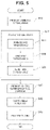
- FIG. 5 is a flowchart of a manufacturing method of the image pickup apparatus according to the first embodiment
- FIG. 6 is a sectional view for explaining the manufacturing method of the image pickup apparatus according to the first embodiment
- FIG. 7 is a sectional view for explaining the manufacturing method of the image pickup apparatus according to the first embodiment
- FIG. 8 is a sectional view for explaining the manufacturing method of the image pickup apparatus according to the first embodiment
- FIG. 9 is a sectional view for explaining the manufacturing method of the image pickup apparatus according to the first embodiment.
- FIG. 10 is a sectional view for explaining the manufacturing method of the image pickup apparatus according to the first embodiment
- FIG. 11 is a sectional view for explaining the manufacturing method of the image pickup apparatus according to the first embodiment
- FIG. 12 is a perspective exploded view for explaining the manufacturing method of the image pickup apparatus according to the first embodiment
- FIG. 13 is a sectional view for explaining the manufacturing method of the image pickup apparatus according to the first embodiment
- FIG. 14 is a sectional view of a holding portion of an image pickup apparatus according to a first modification of the first embodiment
- FIG. 15 is a sectional view of a holding portion of an image pickup apparatus according to a second modification of the first embodiment
- FIG. 16 is a sectional view of an image pickup apparatus according to a second embodiment
- FIG. 17 is a sectional view of an image pickup apparatus according to a third embodiment.
- FIG. 18 is a perspective view of an image pickup apparatus according to a fourth embodiment.
- an endoscope system 8 including an endoscope 9 is provided with the endoscope 9 , a processor 80 , a light source device 81 , and a monitor 82 .
- the endoscope 9 includes an insertion portion 90 , an operation portion 91 , and a universal cord 92 .
- the endoscope 9 is adapted such that an insertion portion 90 is inserted into a body cavity of a subject to photograph an image inside the body of the subject and output an image signal.
- the insertion portion 90 is configured of a distal end portion 90 A at which an image pickup apparatus 1 is disposed, a bending portion 90 B that is continuously provided at a proximal end portion of the distal end portion 90 A to be bendable, and a flexible portion 90 C that is continuously provided at a proximal end portion of the bending portion 90 B.
- the bending portion 90 B is bent in response to an operation of the operation portion 91 .
- the endoscope 9 is a flexible endoscope for medical use, the endoscope 9 may be a rigid endoscope, may be an endoscope for industrial use, or may be an endoscope of a capsule type.
- the operation portion 91 in which various buttons for operating the endoscope 9 are provided is disposed at a proximal end portion of the insertion portion 90 of the endoscope 9 .
- the light source device 81 includes, for example, a white LED. Illumination light that the light source device 81 emits is guided to the distal end portion 90 A by passing through a light guide (not illustrated) that allows insertion of the universal cord 92 and the insertion portion 90 to illuminate the subject.
- the endoscope 9 transmits an image pickup signal that the image pickup apparatus 1 disposed at the distal end portion 90 A of the insertion portion 90 outputs via a signal cable 94 that allows insertion of the insertion portion 90 .
- the image pickup apparatus 1 for an endoscope has an ultrasmall size, and the distal end portion 90 A of the insertion portion 90 thus has a diameter of less than 3 mm, for example, the endoscope 9 is minimally invasive.
- the image pickup apparatus 1 As illustrated in FIGS. 2 to 4 , the image pickup apparatus 1 according to the embodiment is provided with a laminated optical portion (first member) 10 , an image pickup unit (second member) 30 , and a holding portion (third member: holder) 20 .
- the laminated optical portion 10 in which a plurality of optical members 11 to 16 are laminated is an optical part that includes an incident surface (front surface) 10 SA on which light is incident and an emission surface (back surface) 10 SB on the opposite side of the incident surface 10 SA.
- the optical members 11 and 14 are lens members.
- the optical member 16 is a parallel flat plate filter made of an infrared cutting material that removes infrared rays.
- the optical members 13 and 15 are spacers in which portions that serve as optical paths are through-holes.
- the laminated optical portion 10 that is a wafer level laminated body has a rectangular parallelepiped shape that has, as a cut surface, an optical side surface 10 SS that is a side surface.
- the image pickup unit 30 that includes a cover glass 31 and an image pickup device 32 includes a front surface 30 SA (cover glass front surface 31 SA) and a back surface 30 SB on the opposite side of the front surface 30 SA, and a plurality of external electrodes 30 P are disposed on the back surface 30 SB (image pickup device back surface 32 SB).
- the image pickup device 32 includes a light receiving portion 32 A that is configured of a CCD or CMOS image pickup unit, and the light receiving portion 32 A is connected to a penetrating wiring (not illustrated).
- the image pickup device 32 may be either a front surface irradiation-type image sensor or a back surface irradiation-type image sensor.
- the light receiving portion 32 A is connected to the external electrodes 30 P on the back surface 30 SB via the penetrating wiring. Although not illustrated, the external electrodes 30 P are electrically connected to the signal cable 94 .
- the image pickup unit 30 that is a wafer level laminated body has a rectangular parallelepiped shape that has, as a cut surface, an image pickup side surface 30 SS that is a side surface.
- the holding portion 20 is made of Silicon on Insulator (SOI) including a spacer 21 , a frame 23 , and a silicon oxide layer 22 that is an intermediate layer.
- the spacer 21 made of silicon has a first main surface 21 SA and a second main surface 21 SB on an opposite side of the first main surface 21 SA.
- the frame 23 made of silicon has a third main surface 23 SA and a fourth main surface 23 SB on an opposite side of the third main surface 23 SA.
- the silicon oxide layer 22 that is an insulating layer bonds the second main surface 21 SB and the third main surface 23 SA In other words, the third main surface 23 SA and the second main surface 21 SB face each other.
- the holding portion 20 produced from an SOT wafer has a rectangular parallelepiped shape that has, as a cut surface, a holding side surface 20 SS that is a side surface.
- the holding portion 20 is a frame body in which a first through-hole H 21 that penetrates through the spacer 21 , a second through-hole H 23 that penetrates through the frame 23 , and a third through-hole H 22 that penetrates through the silicon oxide layer 22 .
- a through-hole H 20 that penetrates through the holding portion 20 is configured by the first through-hole H 21 , the second through-hole H 23 , and the third through-hole 122 .
- the first through-hole H 21 , the second through-hole H 23 , and the third through-hole H 22 communicate with each other, and these form an optical path between the laminated optical portion 10 and the image pickup unit 30 .
- the diameter of the first through-hole H 21 is substantially the same as the outer dimension of the light receiving portion 32 A.
- the inner dimension of the second through-hole H 23 is slightly larger than the outer dimension of the image pickup unit 30 .
- the second through-hole H 23 and the third through-hole H 22 have larger sectional areas in a direction that perpendicularly intersects an optical axis than the sectional area of the first through-hole H 21 .
- the first through-hole H 21 has a circular section in the direction that perpendicularly intersects the optical axis, and the second through-hole H 23 and the third through-hole H 22 have rectangular sections.
- a first main surface 20 SA ( 21 SA) of the holding portion 20 is glued to the emission surface 10 SB of the laminated optical portion 10 with an adhesive layer 50 .
- the image pickup unit 30 is disposed in the second through-hole H 23 and the third through-hole H 2 , and the front surface 30 SA of the image pickup unit 30 abuts on the second main surface 21 SB of the spacer 21 .
- An adhesive 40 is disposed between the image pickup side surface 30 SS and a wall surface 20 HSS of the second through-hole H 23 while no adhesive 40 is disposed between the front surface 30 SA and the second main surface 21 SB.
- the front surface 30 SA and the second main surface 21 SB are in direct surface contact with each other with no other member interposed between the front surface 30 SA and the second main surface 21 SB.
- the image pickup apparatus 1 has a square sectional shape that perpendicularly intersects an optical axis O, for example, and the dimension (outer dimension) is as ultrasmall as 1 mm square or less.
- the dimension (outer dimension) of the image pickup unit 30 in the direction that perpendicularly intersects the optical axis is, for example, 0.5 mm square or less. Therefore, it is not easy to dispose the image pickup unit 30 directly on the emission surface 10 SB of the laminated optical portion 10 . On the other hand, it is easy to insert the image pickup unit 30 into the second through-hole H 23 of the holding portion 20 even if the size of the image pickup unit 30 is small. Further, positioning of the image pickup unit 30 in an in-plane direction (XY direction: see FIG. 4 ) that perpendicularly intersects the optical axis is automatically performed by inserting the image pickup unit 30 into the second through-hole H 23 .
- the position of the light receiving portion 32 A (light receiving surface 32 SA) of the image pickup unit 30 in the direction of the optical axis O (Z direction: see FIG. 4 ) is preferably positioned with precision of an error of 1 ⁇ m or less, for example, relative to the focal position of the laminated optical portion 10 in order to obtain a satisfactory image.
- the distance from the emission surface 10 SB of the laminated optical portion 10 to the light receiving portion 32 A is defined by the thickness of the adhesive layer 50 and the thickness of the spacer 21 . It is possible to easily realize the production of the adhesive layer 50 and the spacer 21 with thicknesses with precision of an error of 1 ⁇ m or less using a known spin coating technique for the adhesive layer 50 or a known polishing technique for the spacer 21 .
- the position of the light receiving portion 32 A (light receiving surface 32 SA) in the direction of the optical axis is positioned with precision of an error of 1 ⁇ m or less, for example, relative to the focal position of the laminated optical portion 10 by the front surface 30 SA of the image pickup unit 30 abutting on the second main surface 21 SB of the spacer 21 in the image pickup apparatus 1 . Therefore, the image pickup apparatus 1 has high performance.
- the frame 23 made of silicon has a light shielding function of shielding unnecessary light that is incident on an optical path (second through-hole H 23 ) from the image pickup side surface 30 SS of the image pickup unit 30 .
- the image pickup apparatus 1 is not affected by external light and stray light and thus has high performance.
- the back surface 30 SB of the image pickup unit 30 may project from the second through-bole 23 as long as a part of the image pickup device 32 is accommodated in the second through-hole H 23 .
- the image pickup unit 30 it is only necessary for the image pickup unit 30 to be disposed such that at least a part of the image pickup unit 30 is inserted into the second through-hole H 23 .
- the thickness (the dimension in the direction of the optical axis: the depth of the second through-hole) of the frame 23 may be smaller than the thickness of the image pickup unit 30 . It is a matter of course that the entire image pickup unit 30 may be fully accommodated in the second through-hole H 23 .
- the image pickup apparatus 1 has a ultrasmall size and high performance and can easily be manufactured, and the endoscope 9 including the image pickup apparatus 1 is minimally invasive, has high performance, and can easily be manufactured.
- As a material of the spacer and the frame glass, resin, metal, or the like may be used instead of silicon.
- a manufacturing method of the image pickup apparatus will be described in accordance with the flowchart in FIG. 5 .
- Step S 10 Laminated Optical Wafer Production Process (First Process)
- Optical wafers 11 W to 16 W in which the plurality of optical members 11 to 16 are formed, respectively, are produced (see FIG. 12 ).
- the optical wafers 11 W and 14 W are lens wafers formed through resin molding.
- the optical wafers 11 W and 14 W may be hybrid lens wafers in each of which a plurality of resin lenses are disposed on a glass substrate.
- the optical wafer 16 W is a parallel flat plate filter wafer made of an infrared cutting material that removes infrared rays.
- As the filter wafer a transparent wafer in which a bandpass filter that transmits only light with a predetermined wavelength and cuts light with unnecessary wavelengths is disposed on the surface may be used.
- the optical wafers 13 W and 15 W are spacer wafers in which portions that serve as optical paths are through-holes.
- the optical wafers 11 W to 16 W are glued to each other with a transparent adhesive or are bonded directly to each other, thereby producing the laminated optical wafer 10 W with a thickness of 3000 ⁇ m, for example.
- types, materials, shapes (circular shapes, rectangular shapes), thicknesses, the number of laminations, and the order of laminations of the plurality of optical wafers can appropriately be changed.
- Step S 20 Holding Wafer Production Process (Second Process)
- a holding wafer 20 W in which a plurality of the holding portions 20 are disposed in an array shape (two-dimensional matrix shape) is produced.
- the second process includes a process (Step S 21 ) of forming the second through-hole H 23 , a process (Step S 22 ) of forming the first through-hole H 21 , and a process (Step S 23 ) of forming the third through-hole 122 .
- the holding wafer 20 W is produced through etching of an SOI wafer 20 WA including a silicon layer (active layer) 21 W, a silicon oxide layer 22 W, and a silicon substrate 23 W.
- Step S 21 Second Through-Hole Formation Process
- an etching mask 25 made of silicon oxide or photoresist is disposed on a second main surface 20 SB of the SOI wafer WA.
- the second through-hole H 23 with a rectangular section that penetrates through the silicon substrate 23 W is formed as illustrated in FIG. 7 by successively repeating a protective film formation process in which protective film formation gas is introduced and an etching process in which etching gas is introduced.
- the protective film formation gas is C 4 F 8
- etching gas is SF 6 . Since the silicon oxide layer 22 W serves as an etching stop layer, the formed second through-hole H 23 uses the silicon oxide layer 22 W as a bottom surface.
- Step S 22 First Through-Hole Formation Process
- a support plate 28 W including an adhesive layer 27 is glued to the second main surface 20 SB of the SOI wafer 20 WA. Then, an etching mask 26 made of silicon oxide or photoresist is disposed on the first main surface 20 SA of the SOI wafer 20 WA.
- the first through-hole H 21 with a circular section is formed in the silicon layer 21 W.
- the formed first through-hole H 21 uses the silicon oxide layer 22 W as a bottom surface.
- the support plate 28 W is detached from the SOI wafer 20 WA.
- the adhesive layer 27 loses an adhesive force through irradiation with ultraviolet rays, heating, or immersion in a solvent.
- the silicon oxide layer 22 W at the bottom surface of the first through-hole H 21 (the bottom surface of the second through-hole H 23 ) is removed, and the third through-hole H 22 is formed, thereby forming the through-hole H 20 in the holding portion 20 .
- the holding wafer 20 W is produced by removing the silicon oxide layer 22 W at the bottom surface using a hydrofluoric acid solution that has a higher etching rate for silicon oxide than an etching rate for silicon.
- the third through-hole H 22 has the same shape and the same size as the shape and the size of the second through-hole H 23 .
- the second through-hole formation process (S 21 ) may be performed after the first through-hole formation process (S 22 ).
- the etching masks 25 and 26 may be removed in the third through-hole formation process (S 23 ).
- the laminated optical wafer production process (first process) may be performed after the holding wafer production process (second process).
- Step S 30 Production of Holding Wafer with Optical Portions (Third Process)
- the holding wafer 29 W with the optical portion is produced by gluing the emission surface 10 SB of the laminated optical wafer OW and the first main surface 20 SA of the holding wafer 20 W to each other with the adhesive layer 50 .
- the respective wafers illustrated in FIG. 12 have circular shapes, at least some of the wafers may have rectangular shapes, for example.
- a thickness error of the adhesive layer 50 is 0.1 ⁇ m or less.
- a through hole is preferably formed in advance in the optical path region in the adhesive layer 50 .
- the adhesive layer 50 is pattern-applied by an ink jet method or a metal mask method, or the adhesive layer 50 is glued using a resin containing a photoresist as the adhesive layer 50 , and the adhesive layer 50 in the optical path region is then removed.
- Step S 40 Image Pickup Unit Disposition Process (Fourth Process)
- the image pickup unit 30 is produced by cutting a glass wafer, an image pickup device wafer, and an image pickup wafer.
- the image pickup device wafer in which a plurality of the light receiving portions 32 A are disposed is produced using a known semiconductor manufacturing technique for a silicon wafer.
- a peripheral circuit that performs primary processing on signals outputted from the light receiving portions 32 A or performs processing on drive control signals may be formed in the image pickup device wafer.
- a penetrating wiring connected to the light receiving portions 32 A and the external electrodes 30 P on the back surface 30 SB are formed in the image pickup wafer.
- the image pickup unit 30 is produced by cutting the image pickup wafer. Therefore, four side surfaces (image pickup side surfaces 30 SS) of the image pickup unit 30 are cut surfaces.
- each image pickup unit 30 is disposed in the respective through-holes H 20 in the holding wafer 29 W with the optical portion.
- the outer dimension of each image pickup unit 30 (the section size in the direction that perpendicularly intersects the optical axis) is smaller than the second through-hole H 23 (third through-hole H 22 ) in the frame 23 and is larger than the first through-hole H 21 in the spacer 21 . Therefore, the front surface 30 SA of the image pickup unit 30 abuts on the second main surface 21 SB of the spacer 21 .
- each image pickup unit 30 is as ultrasmall as 0.5 mm square or less, for example, it is easy to dispose the image pickup unit 30 at a predetermined position in the in-plane direction (XY direction) of the holding wafer 29 W with the optical portion since the second through-hole H 23 is provided.
- the ultraviolet curable adhesive 40 for example, is disposed between the image pickup side surface 30 SS and the wall surface 20 HSS of the second through-hole H 23 , and curing processing using irradiation with ultraviolet rays is performed.
- the adhesive 40 may be a thermosetting adhesive or may be an adhesive that is cured through irradiation with ultraviolet rays and heating, or two types, namely the ultraviolet curable adhesive and the thermosetting adhesive may be used in combination.
- the section of the first through-hole H 21 may have a rectangular shape.
- the section of the first through-hole H 21 preferably has a circular shape for easiness of widening the area of an abutting surface between the front surface 30 SA of the image pickup unit 30 and the second main surface 21 SB of the spacer 21 .
- the first through-hole H 21 of the spacer 21 has a circular shape with a diameter of 0.50 mm, for example, it is possible to cause the front surface 30 S of the image pickup unit 30 with a square shape with a side of 0.50 mm to abut on the second main surface 21 SB of the spacer 21 .
- positioning of the image pickup unit 30 in the in-plane direction that perpendicularly intersects the optical axis can be defined merely by disposing the image pickup unit 30 in the second through-hole H 23 . If the image pickup side surface 30 SS of the parallelepiped shape and the wall surface 20 HSS of the second through-hole H 23 with a rectangular section are separated from each other by 5 ⁇ m, for example, positioning with precision of 2.5 ⁇ m is automatically performed. Therefore, the section of the second through-hole H 23 preferably has a rectangular shape.
- the position of the image pickup unit 30 inserted into the second through-hole H 23 is finely adjusted, and then adhesion is performed.
- the thickness of the silicon layer 21 W that serves as the spacer 21 is set on the basis of the focal position of the laminated optical portion 10 .
- the focal position is located at 50 ⁇ m from the emission surface 10 SB, and the thickness of the adhesive layer 50 is 1 ⁇ m, for example, the thickness of the silicon layer 21 W is set to 49 ⁇ m.
- Step S 15 a measurement process of measuring the focal position of the laminated optical portion 10 after the production of the laminated optical wafer 10 W
- a polishing process Step S 16 ) of working the silicon layer 21 W that serves as the spacer 21 of the holding wafer 20 W into a predetermined thickness on the basis of the measured focal position.
- the polishing process is preferably performed prior to the process (S 20 ) of forming the through-hole H 20 in the SOI wafer 20 WA.
- the focal position of the laminated optical portion 10 is located at 45 ⁇ m from the emission surface 10 SB, and the thickness of the adhesive layer 50 is 1 ⁇ m, for example, the silicon layer 21 W with the thickness of 49 ⁇ m is polished to have a thickness of 44 ⁇ m.
- a plurality of image pickup units with different specifications may be disposed in one holding wafer 29 W with the optical portion.
- a plurality of second through-holes with different sizes may be formed in the holding wafer.
- a plurality of the image pickup apparatuses 1 are produced by cutting the holding wafer 29 W with optical portions on which the plurality of image pickup units 30 are disposed using a dicing blade 75 .
- the laminated optical portion 10 and the holding portion 20 are cut in the same cutting process. Therefore, the optical side surface 10 SS that is a side surface of the laminated optical portion 10 and the holding side surface 20 SS that is a side surface of the holding portion 20 are in the same plane. Further, since the optical side surface 10 SS and the holding side surface 20 SS are cut surfaces, continuous cut marks are included in both the optical side surface 10 SS and the holding side surface 20 SS. The cut marks are minute linear irregularities generated on the cut surfaces in the dicing.
- the silicon oxide layer 22 is also cut at the same time with the laminated optical portion 10 and the holding portion 20 . Therefore, the side surface of the silicon oxide layer 22 is in the same plane as the optical side surface 10 SS and the holding side surface 20 SS and includes a continuous cut mark.
- the manufacturing method of the image pickup apparatus 1 it is possible to easily manufacture the ultrasmall image pickup apparatus 1 .
- a notch (recession) N 23 is provided at an outer peripheral edge of an opening of the second through-hole H 23 in the third main surface 23 SA of the frame 23 .
- the notch N 23 that is a cut portion is an overetched region formed when the second through-hole H 23 is formed.
- the notch N 23 can effectively prevent the adhesive 40 from entering the abutting surface between the front surface 30 SA and the second main surface 21 SB when the uncured adhesive 40 is poured between the image pickup side surface 30 SS and the wall surface 20 HSS of the second through-hole H 23 . In other words, since the excessive adhesive 40 is accommodated in the notch N 23 and does not spread on the abutting surface.
- a notch N 20 that is parallel to the optical axis is provided in the wall surface 20 HSS of the second through-hole H 23 in the frame 23 .
- the notch N 20 is a groove in the wall surface 20 HSS extending from the fourth main surface 23 SB of the frame 23 to the second main surface 21 SB of the spacer 21 .
- the second through-hole H 23 and the image pickup unit 30 have substantially the same sizes, there may be a case in which it is not easy to dispose the adhesive 40 in the gap. However, it is easy to secure the image pickup unit 30 to the second through-hole H 23 by pouring the adhesive 40 into the notch N 20 . Note that it is not necessary for the portion between the second through-hole H 23 and the image pickup unit 30 to be filled with the adhesive 40 with no gap, and it is possible to secure the image pickup unit 30 to the second through-hole H 23 as long as the adhesive 40 is disposed at least in a part of the notch N 20 .
- a small amount of ultraviolet curable resin may be disposed in the notch N 20 to temporarily secure the image pickup unit 30 to the second through-hole H 23 after the image pickup unit 30 is inserted into the second through-hole H 23 and positioning in the in-plane direction is performed.
- the adhesive 40 may be disposed after all the image pickup units 30 are temporarily secured to the holding wafer 29 W with optical portions.
- the holding portion 20 may include at least one notch N 20 in the wall surface 20 HSS, a plurality of notches N 20 may be provided.
- the shape of the notch N 20 is not limited to the shape in the illustrated example and may be a curved shape or the like.
- image pickup apparatuses 1 A to 1 C are similar to the image pickup apparatus 1 and have similar advantages, the same reference signs will be applied to components with the same functions, and description will be omitted.
- the image pickup apparatus 1 A illustrated in FIG. 16 includes no silicon oxide layer between a spacer 21 and a frame 23 of a holding portion 20 A.
- a holding wafer 20 W is produced through bonding of two silicon wafers.
- a first silicon wafer in which a first through-hole H 21 is formed and a second silicon wafer in which a second through-hole H 23 is formed are bonded directly to each other, thereby producing the holding wafer 20 W.
- the silicon oxide layer is not an essential component of the holding wafer 20 W (holding portion 20 ).
- the holding portion it is only necessary for the holding portion to include the spacer 21 and the frame 23 .
- the image pickup apparatus 1 B illustrated in FIG. 17 further includes a laminated semiconductor 39 bonded to a back surface 30 SB of an image pickup unit 30 .
- the laminated semiconductor 39 in which a plurality of semiconductor devices 33 to 35 are laminated is disposed in a second through-hole H 23 .
- the semiconductor devices 33 to 35 perform primary processing on image pickup signals outputted from an image pickup device 32 and perform processing on control signals for controlling the image pickup device 32 .
- the semiconductor devices 33 to 35 include an AD conversion circuit, a memory, a transmission output circuit, a filter circuit, a capacitor, a resistor, or an inductor.
- the number of semiconductor devices included in the laminated semiconductor 39 is, for example, equal to or greater than one and equal to or less than ten.
- Each of the plurality of semiconductor devices 33 to 35 is electrically connected via a penetrating wiring (not illustrated).
- a manufacturing method of the image pickup apparatus 1 B a plurality of device wafers, in each of which the plurality of semiconductor devices 33 to 35 are formed, are produced. Then, the plurality of device wafers are laminated, thereby producing the laminated device wafer.
- the image pickup unit 30 to which the laminated semiconductor 39 is bonded is produced by bonding and then cutting the image pickup wafer and the laminated device wafer.
- the image pickup apparatus 1 B has high mechanical strength against a stress in the direction that perpendicularly intersects the optical axis since the image pickup unit 30 and the laminated semiconductor 39 are disposed in the second through-hole H 23 .
- the frame 23 has a reinforcing function for improving the mechanical strength of the laminated semiconductor 39 . It is a matter of course that the image pickup apparatus 1 B has higher performance than the image pickup apparatuses 1 and 1 A since the image pickup apparatus 1 B has the laminated semiconductor 39 .
- the laminated semiconductor 39 it is not necessary for the entire laminated semiconductor 39 to be fully accommodated in the second through-hole H 23 , and for example, a part of the semiconductor device 35 located at the backmost surface may project from the second through-hole H 23 . In other words, it is only necessary for the laminated semiconductor 39 to be disposed such that at least a part of the laminated semiconductor 39 is inserted into the second through-hole H 23 .
- the image pickup apparatus 1 B is provided with a light shielding layer 70 that covers an optical side surface 10 SS and a holding side surface 20 SS.
- the light shielding layer 70 is disposed by filling a groove formed by a known step cut dicing method, for example, with a light shielding resin.
- the groove is formed along a cut line using a first dicing blade with a cutting margin of a first width in a process (S 50 ) of cutting the holding wafer 29 W with optical portions in which the plurality of image pickup units 30 are disposed. Then, the groove is filled with a resin containing a light shielding material such as carbon particles, for example. Then, cutting is performed using a second dicing blade with a cutting margin that is narrower than the first width, thereby producing the image pickup apparatus 1 B with the light shielding layer 70 provided on the side surface.
- the direction in which the groove is formed using the first dicing blade may be opposite.
- the light shielding layer 70 may be a metal layer disposed in the groove by a plating method or a sputtering method and may be disposed after the cutting process (S 50 ).
- the image pickup apparatus 1 B provided with the light shielding layer 70 is not affected by external light and thus has high performance.
- the image pickup apparatuses 1 and 1 A also have the same advantages as the advantages of the image pickup apparatus 1 B as long as the image pickup apparatuses 1 and 1 A also include light shielding layers 70 that cover the optical side surfaces 10 SS and the holding side surfaces 20 SS similarly to the image pickup apparatus 1 B.
- outer shapes of a laminated optical portion 10 and a holding portion 20 are hexagonal columns.
- Outer shapes of the laminated optical portion and the holding portion corresponding to a wafer level laminated body are hexagonal columns obtained by chamfering corners of sides of quadrangular columns. Note that quadrangular columns may be chamfered into curved surface shapes, thereby obtaining cylindrical shapes.
- the image pickup apparatus 1 C in which the outer shapes of the laminated optical portion and the holding portion are hexagonal columns that are polygonal columns can be disposed in a space that is narrower than a space for the image pickup apparatus 1 , the image pickup apparatus 1 C is effective for reducing the diameter (reducing invasiveness) of the endoscope.
- the outer shapes of the laminated optical portions 10 and the holding portions 20 in the image pickup apparatuses 1 , 1 A, and 1 B are also not limited to the rectangular parallelepiped shapes.
- the endoscopes that include the image pickup apparatuses 1 A to 1 C have the effects of the endoscope 9 that includes the image pickup apparatus 1 and further have the effects of the image pickup apparatuses 1 A to 1 C.
Landscapes
- Physics & Mathematics (AREA)
- Engineering & Computer Science (AREA)
- Optics & Photonics (AREA)
- Health & Medical Sciences (AREA)
- Life Sciences & Earth Sciences (AREA)
- General Physics & Mathematics (AREA)
- Surgery (AREA)
- Multimedia (AREA)
- Signal Processing (AREA)
- Radiology & Medical Imaging (AREA)
- Animal Behavior & Ethology (AREA)
- Pathology (AREA)
- Biophysics (AREA)
- Astronomy & Astrophysics (AREA)
- Biomedical Technology (AREA)
- Heart & Thoracic Surgery (AREA)
- Medical Informatics (AREA)
- Molecular Biology (AREA)
- Nuclear Medicine, Radiotherapy & Molecular Imaging (AREA)
- General Health & Medical Sciences (AREA)
- Public Health (AREA)
- Veterinary Medicine (AREA)
- Manufacturing & Machinery (AREA)
- Endoscopes (AREA)
- Solid State Image Pick-Up Elements (AREA)
- Transforming Light Signals Into Electric Signals (AREA)
Abstract
Description
Claims (12)
Applications Claiming Priority (1)
| Application Number | Priority Date | Filing Date | Title |
|---|---|---|---|
| PCT/JP2018/017096 WO2019207739A1 (en) | 2018-04-26 | 2018-04-26 | Imaging device, endoscope, and method for manufacturing imaging device |
Related Parent Applications (1)
| Application Number | Title | Priority Date | Filing Date |
|---|---|---|---|
| PCT/JP2018/017096 Continuation WO2019207739A1 (en) | 2018-04-26 | 2018-04-26 | Imaging device, endoscope, and method for manufacturing imaging device |
Publications (2)
| Publication Number | Publication Date |
|---|---|
| US20210099620A1 US20210099620A1 (en) | 2021-04-01 |
| US11412113B2 true US11412113B2 (en) | 2022-08-09 |
Family
ID=68295118
Family Applications (1)
| Application Number | Title | Priority Date | Filing Date |
|---|---|---|---|
| US17/079,628 Active US11412113B2 (en) | 2018-04-26 | 2020-10-26 | Image pickup apparatus, endoscope, and manufacturing method of image pickup apparatus |
Country Status (3)
| Country | Link |
|---|---|
| US (1) | US11412113B2 (en) |
| CN (1) | CN112041721B (en) |
| WO (1) | WO2019207739A1 (en) |
Families Citing this family (2)
| Publication number | Priority date | Publication date | Assignee | Title |
|---|---|---|---|---|
| WO2020129185A1 (en) * | 2018-12-19 | 2020-06-25 | オリンパス株式会社 | Imaging device and method for manufacturing imaging device |
| WO2022167512A1 (en) * | 2021-02-05 | 2022-08-11 | Richard Wolf Gmbh | Endoscopic instrument |
Citations (9)
| Publication number | Priority date | Publication date | Assignee | Title |
|---|---|---|---|---|
| WO2010033211A1 (en) | 2008-09-18 | 2010-03-25 | Tessera North America, Inc. | Recessed optical surfaces |
| WO2010101009A1 (en) | 2009-03-02 | 2010-09-10 | コニカミノルタオプト株式会社 | Lens unit, method for aligning lens unit and sensor, image pickup device, method for manufacturing image pickup device, and wafer lens unit |
| WO2010140395A1 (en) | 2009-06-05 | 2010-12-09 | コニカミノルタオプト株式会社 | Imaging device and method of producing imaging device |
| JP2011085625A (en) | 2009-10-13 | 2011-04-28 | Toppan Printing Co Ltd | Camera module and method for manufacturing the same |
| JP2013037244A (en) | 2011-08-09 | 2013-02-21 | Sharp Corp | Lens device and electronic apparatus |
| US20170027421A1 (en) * | 2015-01-27 | 2017-02-02 | Olympus Corporation | Endoscope |
| WO2017203593A1 (en) | 2016-05-24 | 2017-11-30 | オリンパス株式会社 | Method for manufacturing endoscope optical unit, endoscope optical unit, and endoscope |
| US20170374252A1 (en) | 2016-06-25 | 2017-12-28 | Omnivision Technologies, Inc. | Bezels For Die Level Packaging Of Camera Modules, And Associated Camera Modules And Methods |
| US20190373147A1 (en) * | 2017-01-26 | 2019-12-05 | Sony Semiconductor Solutions Corporation | Camera module, method of producing the same, and electronic device |
Family Cites Families (4)
| Publication number | Priority date | Publication date | Assignee | Title |
|---|---|---|---|---|
| EP2698094B1 (en) * | 2012-03-06 | 2015-09-02 | Olympus Medical Systems Corp. | Image pickup unit for endoscope |
| DE102014208652A1 (en) * | 2014-05-08 | 2015-11-12 | Olympus Winter & Ibe Gmbh | Videoscope |
| WO2016139841A1 (en) * | 2015-03-04 | 2016-09-09 | オリンパス株式会社 | Suction power adjusting device for ultrasound observation and ultrasound endoscope |
| US9829698B2 (en) * | 2015-08-31 | 2017-11-28 | Panasonic Corporation | Endoscope |
-
2018
- 2018-04-26 CN CN201880092644.4A patent/CN112041721B/en active Active
- 2018-04-26 WO PCT/JP2018/017096 patent/WO2019207739A1/en not_active Ceased
-
2020
- 2020-10-26 US US17/079,628 patent/US11412113B2/en active Active
Patent Citations (11)
| Publication number | Priority date | Publication date | Assignee | Title |
|---|---|---|---|---|
| WO2010033211A1 (en) | 2008-09-18 | 2010-03-25 | Tessera North America, Inc. | Recessed optical surfaces |
| US20120229908A1 (en) | 2008-09-18 | 2012-09-13 | Digitaloptics Corporation East | Recessed optical surfaces |
| WO2010101009A1 (en) | 2009-03-02 | 2010-09-10 | コニカミノルタオプト株式会社 | Lens unit, method for aligning lens unit and sensor, image pickup device, method for manufacturing image pickup device, and wafer lens unit |
| WO2010140395A1 (en) | 2009-06-05 | 2010-12-09 | コニカミノルタオプト株式会社 | Imaging device and method of producing imaging device |
| JP2011085625A (en) | 2009-10-13 | 2011-04-28 | Toppan Printing Co Ltd | Camera module and method for manufacturing the same |
| JP2013037244A (en) | 2011-08-09 | 2013-02-21 | Sharp Corp | Lens device and electronic apparatus |
| JP5474890B2 (en) | 2011-08-09 | 2014-04-16 | シャープ株式会社 | LENS DEVICE AND ELECTRONIC DEVICE |
| US20170027421A1 (en) * | 2015-01-27 | 2017-02-02 | Olympus Corporation | Endoscope |
| WO2017203593A1 (en) | 2016-05-24 | 2017-11-30 | オリンパス株式会社 | Method for manufacturing endoscope optical unit, endoscope optical unit, and endoscope |
| US20170374252A1 (en) | 2016-06-25 | 2017-12-28 | Omnivision Technologies, Inc. | Bezels For Die Level Packaging Of Camera Modules, And Associated Camera Modules And Methods |
| US20190373147A1 (en) * | 2017-01-26 | 2019-12-05 | Sony Semiconductor Solutions Corporation | Camera module, method of producing the same, and electronic device |
Non-Patent Citations (1)
| Title |
|---|
| International Search Report dated Aug. 7, 2018 issued in PCT/JP2018/017096. |
Also Published As
| Publication number | Publication date |
|---|---|
| WO2019207739A1 (en) | 2019-10-31 |
| CN112041721A (en) | 2020-12-04 |
| CN112041721B (en) | 2022-05-06 |
| US20210099620A1 (en) | 2021-04-01 |
Similar Documents
| Publication | Publication Date | Title |
|---|---|---|
| JP6640341B2 (en) | Manufacturing method of optical unit for endoscope, optical unit for endoscope, and endoscope | |
| US12015045B2 (en) | Manufacturing method of image pickup apparatus for endoscope, image pickup apparatus for endoscope, and endoscope | |
| WO2020148860A1 (en) | Manufacturing method of imaging device for endoscope, imaging device for endoscope, and endoscope | |
| WO2016117120A1 (en) | Image pickup device and endoscope | |
| US11412113B2 (en) | Image pickup apparatus, endoscope, and manufacturing method of image pickup apparatus | |
| WO2018198266A1 (en) | Endoscope, imaging module, and method for manufacturing imaging module | |
| WO2019138440A1 (en) | Imaging device, endoscope, and manufacturing method for imaging device | |
| JP2018050769A (en) | An optical element, an endoscope optical unit, an endoscope, and a method of manufacturing an endoscope optical unit. | |
| WO2021176512A1 (en) | Endoscope, optical laiminate, and method for manufacturing optical laminate | |
| JPWO2017179144A1 (en) | Method of manufacturing optical unit for endoscope and endoscope | |
| WO2015141577A1 (en) | Optical fiber holding member, endoscope and method for producing optical fiber holding member | |
| US12416799B2 (en) | Endoscope lens unit, endoscope, and manufacturing method of endoscope lens unit | |
| US12495199B2 (en) | Image pickup unit, endoscope, and method for manufacturing image pickup unit | |
| JP7627764B2 (en) | Imaging device and endoscope | |
| WO2020230261A1 (en) | Method for manufacturing endoscope imaging device, endoscope imaging device, and endoscope | |
| US20210137372A1 (en) | Image pickup apparatus for endoscope and endoscope | |
| WO2019171460A1 (en) | Endoscope imaging device, endoscope, and method of manufacturing endoscope imaging device | |
| US12487444B2 (en) | Optical unit, manufacturing method for optical unit, and endoscope | |
| CN116529886A (en) | Laminated lens, optical unit, endoscope, and method for manufacturing optical unit | |
| JP7456072B2 (en) | Lens unit manufacturing method, lens unit, imaging device, and endoscope | |
| US20230225585A1 (en) | Image pickup unit, endoscope, and method for manufacturing image pickup unit | |
| US11287641B2 (en) | Image pickup apparatus, endoscope, and method for manufacturing image pickup apparatus | |
| WO2019138463A1 (en) | Method for manufacturing optical unit, optical unit, and endoscope | |
| JP2019153698A (en) | Endoscope imaging apparatus, endoscope, and manufacturing method of endoscope imaging apparatus |
Legal Events
| Date | Code | Title | Description |
|---|---|---|---|
| FEPP | Fee payment procedure |
Free format text: ENTITY STATUS SET TO UNDISCOUNTED (ORIGINAL EVENT CODE: BIG.); ENTITY STATUS OF PATENT OWNER: LARGE ENTITY |
|
| AS | Assignment |
Owner name: OLYMPUS CORPORATION, JAPAN Free format text: ASSIGNMENT OF ASSIGNORS INTEREST;ASSIGNOR:IGARASHI, TAKATOSHI;REEL/FRAME:054705/0049 Effective date: 20201126 |
|
| STPP | Information on status: patent application and granting procedure in general |
Free format text: APPLICATION DISPATCHED FROM PREEXAM, NOT YET DOCKETED |
|
| STPP | Information on status: patent application and granting procedure in general |
Free format text: DOCKETED NEW CASE - READY FOR EXAMINATION |
|
| STPP | Information on status: patent application and granting procedure in general |
Free format text: NON FINAL ACTION MAILED |
|
| STPP | Information on status: patent application and granting procedure in general |
Free format text: RESPONSE TO NON-FINAL OFFICE ACTION ENTERED AND FORWARDED TO EXAMINER |
|
| STPP | Information on status: patent application and granting procedure in general |
Free format text: NOTICE OF ALLOWANCE MAILED -- APPLICATION RECEIVED IN OFFICE OF PUBLICATIONS |
|
| STCF | Information on status: patent grant |
Free format text: PATENTED CASE |
|
| MAFP | Maintenance fee payment |
Free format text: PAYMENT OF MAINTENANCE FEE, 4TH YEAR, LARGE ENTITY (ORIGINAL EVENT CODE: M1551); ENTITY STATUS OF PATENT OWNER: LARGE ENTITY Year of fee payment: 4 |