US11398564B2 - Semiconductor device - Google Patents
Semiconductor device Download PDFInfo
- Publication number
- US11398564B2 US11398564B2 US17/198,050 US202117198050A US11398564B2 US 11398564 B2 US11398564 B2 US 11398564B2 US 202117198050 A US202117198050 A US 202117198050A US 11398564 B2 US11398564 B2 US 11398564B2
- Authority
- US
- United States
- Prior art keywords
- semiconductor region
- electrode
- metal member
- semiconductor
- type semiconductor
- Prior art date
- Legal status (The legal status is an assumption and is not a legal conclusion. Google has not performed a legal analysis and makes no representation as to the accuracy of the status listed.)
- Active
Links
Images


Classifications
-
- H—ELECTRICITY
- H10—SEMICONDUCTOR DEVICES; ELECTRIC SOLID-STATE DEVICES NOT OTHERWISE PROVIDED FOR
- H10D—INORGANIC ELECTRIC SEMICONDUCTOR DEVICES
- H10D12/00—Bipolar devices controlled by the field effect, e.g. insulated-gate bipolar transistors [IGBT]
- H10D12/411—Insulated-gate bipolar transistors [IGBT]
- H10D12/441—Vertical IGBTs
- H10D12/461—Vertical IGBTs having non-planar surfaces, e.g. having trenches, recesses or pillars in the surfaces of the emitter, base or collector regions
- H10D12/481—Vertical IGBTs having non-planar surfaces, e.g. having trenches, recesses or pillars in the surfaces of the emitter, base or collector regions having gate structures on slanted surfaces, on vertical surfaces, or in grooves, e.g. trench gate IGBTs
-
- H—ELECTRICITY
- H10—SEMICONDUCTOR DEVICES; ELECTRIC SOLID-STATE DEVICES NOT OTHERWISE PROVIDED FOR
- H10D—INORGANIC ELECTRIC SEMICONDUCTOR DEVICES
- H10D30/00—Field-effect transistors [FET]
- H10D30/60—Insulated-gate field-effect transistors [IGFET]
- H10D30/64—Double-diffused metal-oxide semiconductor [DMOS] FETs
- H10D30/66—Vertical DMOS [VDMOS] FETs
- H10D30/665—Vertical DMOS [VDMOS] FETs having edge termination structures
-
- H01L29/7397—
-
- H01L23/49562—
-
- H01L29/7813—
-
- H—ELECTRICITY
- H10—SEMICONDUCTOR DEVICES; ELECTRIC SOLID-STATE DEVICES NOT OTHERWISE PROVIDED FOR
- H10D—INORGANIC ELECTRIC SEMICONDUCTOR DEVICES
- H10D12/00—Bipolar devices controlled by the field effect, e.g. insulated-gate bipolar transistors [IGBT]
- H10D12/411—Insulated-gate bipolar transistors [IGBT]
- H10D12/441—Vertical IGBTs
-
- H—ELECTRICITY
- H10—SEMICONDUCTOR DEVICES; ELECTRIC SOLID-STATE DEVICES NOT OTHERWISE PROVIDED FOR
- H10D—INORGANIC ELECTRIC SEMICONDUCTOR DEVICES
- H10D30/00—Field-effect transistors [FET]
- H10D30/60—Insulated-gate field-effect transistors [IGFET]
- H10D30/64—Double-diffused metal-oxide semiconductor [DMOS] FETs
- H10D30/66—Vertical DMOS [VDMOS] FETs
- H10D30/668—Vertical DMOS [VDMOS] FETs having trench gate electrodes, e.g. UMOS transistors
-
- H—ELECTRICITY
- H10—SEMICONDUCTOR DEVICES; ELECTRIC SOLID-STATE DEVICES NOT OTHERWISE PROVIDED FOR
- H10D—INORGANIC ELECTRIC SEMICONDUCTOR DEVICES
- H10D62/00—Semiconductor bodies, or regions thereof, of devices having potential barriers
- H10D62/10—Shapes, relative sizes or dispositions of the regions of the semiconductor bodies; Shapes of the semiconductor bodies
- H10D62/102—Constructional design considerations for preventing surface leakage or controlling electric field concentration
- H10D62/103—Constructional design considerations for preventing surface leakage or controlling electric field concentration for increasing or controlling the breakdown voltage of reverse-biased devices
- H10D62/105—Constructional design considerations for preventing surface leakage or controlling electric field concentration for increasing or controlling the breakdown voltage of reverse-biased devices by having particular doping profiles, shapes or arrangements of PN junctions; by having supplementary regions, e.g. junction termination extension [JTE]
- H10D62/106—Constructional design considerations for preventing surface leakage or controlling electric field concentration for increasing or controlling the breakdown voltage of reverse-biased devices by having particular doping profiles, shapes or arrangements of PN junctions; by having supplementary regions, e.g. junction termination extension [JTE] having supplementary regions doped oppositely to or in rectifying contact with regions of the semiconductor bodies, e.g. guard rings with PN or Schottky junctions
-
- H—ELECTRICITY
- H10—SEMICONDUCTOR DEVICES; ELECTRIC SOLID-STATE DEVICES NOT OTHERWISE PROVIDED FOR
- H10D—INORGANIC ELECTRIC SEMICONDUCTOR DEVICES
- H10D62/00—Semiconductor bodies, or regions thereof, of devices having potential barriers
- H10D62/10—Shapes, relative sizes or dispositions of the regions of the semiconductor bodies; Shapes of the semiconductor bodies
- H10D62/124—Shapes, relative sizes or dispositions of the regions of semiconductor bodies or of junctions between the regions
-
- H—ELECTRICITY
- H10—SEMICONDUCTOR DEVICES; ELECTRIC SOLID-STATE DEVICES NOT OTHERWISE PROVIDED FOR
- H10D—INORGANIC ELECTRIC SEMICONDUCTOR DEVICES
- H10D64/00—Electrodes of devices having potential barriers
- H10D64/20—Electrodes characterised by their shapes, relative sizes or dispositions
- H10D64/27—Electrodes not carrying the current to be rectified, amplified, oscillated or switched, e.g. gates
- H10D64/311—Gate electrodes for field-effect devices
- H10D64/411—Gate electrodes for field-effect devices for FETs
- H10D64/511—Gate electrodes for field-effect devices for FETs for IGFETs
- H10D64/517—Gate electrodes for field-effect devices for FETs for IGFETs characterised by the conducting layers
- H10D64/519—Gate electrodes for field-effect devices for FETs for IGFETs characterised by the conducting layers characterised by their top-view geometrical layouts
-
- H—ELECTRICITY
- H10—SEMICONDUCTOR DEVICES; ELECTRIC SOLID-STATE DEVICES NOT OTHERWISE PROVIDED FOR
- H10W—GENERIC PACKAGES, INTERCONNECTIONS, CONNECTORS OR OTHER CONSTRUCTIONAL DETAILS OF DEVICES COVERED BY CLASS H10
- H10W40/00—Arrangements for thermal protection or thermal control
- H10W40/70—Fillings or auxiliary members in containers or in encapsulations for thermal protection or control
- H10W40/77—Auxiliary members characterised by their shape
- H10W40/778—Auxiliary members characterised by their shape in encapsulations
-
- H—ELECTRICITY
- H10—SEMICONDUCTOR DEVICES; ELECTRIC SOLID-STATE DEVICES NOT OTHERWISE PROVIDED FOR
- H10W—GENERIC PACKAGES, INTERCONNECTIONS, CONNECTORS OR OTHER CONSTRUCTIONAL DETAILS OF DEVICES COVERED BY CLASS H10
- H10W70/00—Package substrates; Interposers; Redistribution layers [RDL]
- H10W70/40—Leadframes
- H10W70/464—Additional interconnections in combination with leadframes
- H10W70/466—Tape carriers or flat leads
-
- H—ELECTRICITY
- H10—SEMICONDUCTOR DEVICES; ELECTRIC SOLID-STATE DEVICES NOT OTHERWISE PROVIDED FOR
- H10W—GENERIC PACKAGES, INTERCONNECTIONS, CONNECTORS OR OTHER CONSTRUCTIONAL DETAILS OF DEVICES COVERED BY CLASS H10
- H10W70/00—Package substrates; Interposers; Redistribution layers [RDL]
- H10W70/40—Leadframes
- H10W70/481—Leadframes for devices being provided for in groups H10D8/00 - H10D48/00
-
- H—ELECTRICITY
- H10—SEMICONDUCTOR DEVICES; ELECTRIC SOLID-STATE DEVICES NOT OTHERWISE PROVIDED FOR
- H10D—INORGANIC ELECTRIC SEMICONDUCTOR DEVICES
- H10D62/00—Semiconductor bodies, or regions thereof, of devices having potential barriers
- H10D62/10—Shapes, relative sizes or dispositions of the regions of the semiconductor bodies; Shapes of the semiconductor bodies
- H10D62/17—Semiconductor regions connected to electrodes not carrying current to be rectified, amplified or switched, e.g. channel regions
- H10D62/393—Body regions of DMOS transistors or IGBTs
-
- H—ELECTRICITY
- H10—SEMICONDUCTOR DEVICES; ELECTRIC SOLID-STATE DEVICES NOT OTHERWISE PROVIDED FOR
- H10D—INORGANIC ELECTRIC SEMICONDUCTOR DEVICES
- H10D64/00—Electrodes of devices having potential barriers
- H10D64/111—Field plates
- H10D64/117—Recessed field plates, e.g. trench field plates or buried field plates
-
- H—ELECTRICITY
- H10—SEMICONDUCTOR DEVICES; ELECTRIC SOLID-STATE DEVICES NOT OTHERWISE PROVIDED FOR
- H10D—INORGANIC ELECTRIC SEMICONDUCTOR DEVICES
- H10D64/00—Electrodes of devices having potential barriers
- H10D64/20—Electrodes characterised by their shapes, relative sizes or dispositions
- H10D64/23—Electrodes carrying the current to be rectified, amplified, oscillated or switched, e.g. sources, drains, anodes or cathodes
- H10D64/251—Source or drain electrodes for field-effect devices
- H10D64/252—Source or drain electrodes for field-effect devices for vertical or pseudo-vertical devices
- H10D64/2527—Source or drain electrodes for field-effect devices for vertical or pseudo-vertical devices for vertical devices wherein the source or drain electrodes are recessed in semiconductor bodies
-
- H—ELECTRICITY
- H10—SEMICONDUCTOR DEVICES; ELECTRIC SOLID-STATE DEVICES NOT OTHERWISE PROVIDED FOR
- H10W—GENERIC PACKAGES, INTERCONNECTIONS, CONNECTORS OR OTHER CONSTRUCTIONAL DETAILS OF DEVICES COVERED BY CLASS H10
- H10W70/00—Package substrates; Interposers; Redistribution layers [RDL]
- H10W70/40—Leadframes
- H10W70/411—Chip-supporting parts, e.g. die pads
- H10W70/417—Bonding materials between chips and die pads
-
- H—ELECTRICITY
- H10—SEMICONDUCTOR DEVICES; ELECTRIC SOLID-STATE DEVICES NOT OTHERWISE PROVIDED FOR
- H10W—GENERIC PACKAGES, INTERCONNECTIONS, CONNECTORS OR OTHER CONSTRUCTIONAL DETAILS OF DEVICES COVERED BY CLASS H10
- H10W72/00—Interconnections or connectors in packages
- H10W72/90—Bond pads, in general
- H10W72/921—Structures or relative sizes of bond pads
- H10W72/926—Multiple bond pads having different sizes
-
- H—ELECTRICITY
- H10—SEMICONDUCTOR DEVICES; ELECTRIC SOLID-STATE DEVICES NOT OTHERWISE PROVIDED FOR
- H10W—GENERIC PACKAGES, INTERCONNECTIONS, CONNECTORS OR OTHER CONSTRUCTIONAL DETAILS OF DEVICES COVERED BY CLASS H10
- H10W90/00—Package configurations
- H10W90/701—Package configurations characterised by the relative positions of pads or connectors relative to package parts
- H10W90/761—Package configurations characterised by the relative positions of pads or connectors relative to package parts of strap connectors
- H10W90/766—Package configurations characterised by the relative positions of pads or connectors relative to package parts of strap connectors between a chip and a stacked lead frame, conducting package substrate or heat sink
Definitions
- Embodiments described herein relate generally to a semiconductor device.
- a semiconductor device such as a metal-oxide-semiconductor field-effect transistor (MOSFET) or an insulated gate bipolar transistor (IGBT) is used in electric power conversion and the like.
- MOSFET metal-oxide-semiconductor field-effect transistor
- IGBT insulated gate bipolar transistor
- FIG. 1 is a plan view illustrating a semiconductor device according to a first embodiment
- FIG. 2 is a cross-sectional view taken along II-II of FIG. 1 ;
- FIG. 3 is a cross-sectional view taken along of FIG.
- FIG. 4 is a plan view illustrating a semiconductor device according to the first embodiment
- FIG. 5 is a cross-sectional view taken along V-V in FIG. 4 ;
- FIG. 6 is a plan view illustrating portion VI of FIG. 4 ;
- FIG. 7 is a cross-sectional view illustrating a portion of a semiconductor device according to a modification of the embodiment
- FIG. 8 is a cross-sectional view illustrating a portion of a semiconductor device according to a modification of the embodiment
- FIG. 9 is a cross-sectional view illustrating a portion of a semiconductor device according to a modification of the embodiment.
- FIG. 10 is a cross-sectional view illustrating a portion of a semiconductor device according to a second embodiment.
- a semiconductor device includes a first metal member, a semiconductor element, and a second metal member.
- the first metal member is electrically connected to a first terminal.
- the semiconductor element includes a first electrode, a first semiconductor region of a first conductivity type, a second semiconductor region of a second conductivity type, a third semiconductor region of the first conductivity type, a gate electrode, and a second electrode.
- the first electrode is provided on the first metal member and electrically connected to the first metal member.
- the first semiconductor region is provided on the first electrode.
- the second semiconductor region is provided on the first semiconductor region.
- the third semiconductor region is provided on the second semiconductor region.
- the gate electrode faces a portion of the first semiconductor region, the second semiconductor region, and the third semiconductor region via a gate insulating layer in a second direction perpendicular to a first direction.
- the first direction is from the first metal member toward the first electrode.
- the second electrode is provided on the second semiconductor region and the third semiconductor region, and electrically connected to the second semiconductor region and the third semiconductor region.
- a plurality of the second semiconductor regions, a plurality of the third semiconductor regions, and a plurality of the gate electrodes are provided in the second direction in the semiconductor element.
- the second metal member is provided on the second electrode.
- the second metal member is electrically connected to the second electrode and electrically connected to a second terminal.
- the semiconductor element includes a first portion where the second electrode is provided that overlaps the second metal member in the first direction, and a second portion where the second electrode is provided that does not overlap the second metal member in the first direction.
- a length in the second direction of the first semiconductor region between an adjacent pair of the gate electrodes in the second portion is greater than a length in the second direction of the first semiconductor region between an adjacent pair of the gate electrodes in the first portion.
- n + , n ⁇ and p + , p represent relative high and low concentration of impurities. That is, the notation with “+” shows that the impurity concentration is relatively higher than the concentration of the notation without any of “+” and “ ⁇ ”, and the notation with “ ⁇ ” shows that the impurity concentration is relatively lower than the concentration of the notation without any of them.
- These notations represent relative high and low concentration of net impurities after compensation of the impurities, when both of p-type impurity and n-type impurity are included in respective regions.
- the embodiments may be executed by inverting the p-type and the n-type in respective semiconductor regions.
- FIG. 1 is a plan view illustrating a semiconductor device according to a first embodiment.
- FIG. 2 is a cross-sectional view taken along II-II of FIG. 1 .
- FIG. 3 is a cross-sectional view taken along of FIG. 1 .
- a semiconductor device 100 includes a first metal member 1 , a second metal member 2 , a third metal member 3 , a sealing portion 5 , and a semiconductor element 10 .
- the sealing portion 5 is omitted.
- the semiconductor element 10 includes a first electrode 11 , a second electrode 12 , a third electrode 13 , and a semiconductor layer 20 .
- the embodiments will be described using an XYZ orthogonal coordinate system.
- the direction from the first metal member 1 toward the first electrode 11 is defined as the Z-direction (first direction).
- the two directions perpendicular to the Z-direction and orthogonal to one another are defined as the X-direction (second direction) and the Y-direction (third direction).
- the direction from the first metal member 1 toward the first electrode 11 is referred to as “up”, and the opposite direction is referred to as “down”. These directions are based on the relative positional relationship between the first metal member 1 and the first electrode 11 and have no connection to the direction of gravity.
- the first metal member 1 is provided at the lower surface of the semiconductor device 100 .
- the first metal member 1 is electrically connected to a first terminal 1 a .
- the first terminal 1 a is integrally formed with the first metal member 1 .
- the first metal member 1 and the first terminal 1 a may be formed of separate members.
- a plurality of the first terminals 1 a may be provided in the X-direction, with each first terminal 1 a extending in the Y-direction.
- the semiconductor element 10 is, for example, a MOSFET.
- the first electrode 11 is provided on the first metal member 1 and is electrically connected to the first metal member 1 .
- the semiconductor layer 20 is provided on the first electrode 11 .
- the second electrode 12 and the third electrode 13 are provided on the semiconductor layer 20 .
- the third electrode 13 is provided separated from the second electrode 12 and is electrically separated from the second electrode 12 .
- the second metal member 2 is provided on the second electrode 12 and is electrically connected to the second electrode 12 .
- the second metal member 2 is electrically connected to a second terminal 2 a .
- a plurality of the second terminals 2 a may be provided in the X-direction, with each second terminal 2 a extending in the Y-direction.
- the third metal member 3 is provided on the third electrode 13 and electrically connected to the third electrode 13 .
- the third metal member 3 is electrically connected to a third terminal 3 a.
- the first electrode 11 to third electrode 13 are electrically connected to the first metal member 1 to the third metal member 3 via join portion 51 to join portion 53 , respectively.
- the second metal member 2 and the third metal member 3 are electrically connected to the second terminal 2 a and the third terminal 3 a via join portions 54 and 55 , respectively.
- the invention is not limited to this example, and two members may be in contact without a connection portion.
- the second metal member 2 may be integrally formed with the second terminal 2 a .
- the third metal member 3 may be integrally formed with the third terminal 3 a.
- the shapes of the first metal member 1 , the second metal member 2 , and the third metal member 3 are not limited to that illustrated in the example and may be changed as appropriate depending on the application of the semiconductor device 100 . Also, the number and shape of the first terminal 1 a , the second terminal 2 a , and the third terminal 3 a may be changed as appropriate.
- the sealing portion 5 covers the upper surface and side surface of the first metal member 1 , the lower surface and the side surface of the second metal member 2 , the third metal member 3 , and the semiconductor element 10 and seals the semiconductor element 10 .
- the sealing portion 5 may further cover the upper surface of the second metal member 2 .
- a portion of the first terminal 1 a , the second terminal 2 a , and the third terminal 3 a may be not covered by the sealing portion 5 and be exposed to the outside.
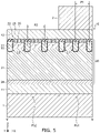
- FIG. 4 is a plan view illustrating a semiconductor device according to the first embodiment.
- FIG. 5 is a cross-sectional view taken along V-V in FIG. 4 .
- the semiconductor element 10 includes a first portion Po 1 and a second portion Po 2 .
- the second electrode 12 is provided in the first portion Po 1 and the second portion Po 2 .
- the first portion Po 1 overlaps the second metal member 2 in the Z-direction.
- the first portion Po 1 is in contact with the second metal member 2 via the join portion 52 .
- the second portion Po 2 does not overlap the second metal member 2 in the Z-direction.
- the second portion Po 2 is located around the first portion Po 1 in the X-Y plane.
- the semiconductor layer 20 includes a n ⁇ -type (first conductivity type) semiconductor region 21 (first semiconductor region), a p-type (second conductivity type) semiconductor region 22 (second semiconductor region), an n + -type semiconductor region 23 (third semiconductor region), an n + -type semiconductor region 24 , a p + -type semiconductor region 25 , and a gate electrode 30 .
- the n + -type semiconductor region 24 is provided on the first electrode 11 and electrically connected to the first electrode 11 .
- the n ⁇ -type semiconductor region 21 is provided on the n + -type semiconductor region 24 .
- the n ⁇ -type semiconductor region 21 is electrically connected to the first electrode 11 via the n + -type semiconductor region 24 .
- the n-type impurity concentration in the n ⁇ -type semiconductor region 21 is lower than the n-type impurity concentration in the n + -type semiconductor region 24 .
- the p-type semiconductor region 22 is provided on the n ⁇ -type semiconductor region 21 .
- the n + -type semiconductor region 23 and the n + -type semiconductor region 25 are provided on the p-type semiconductor region 22 .
- the p-type impurity concentration in the p + -type semiconductor region 25 is higher than the p-type impurity concentration in the p-type semiconductor region 22 .
- the gate electrode 30 faces a portion of the n ⁇ -type semiconductor region 21 , the p-type semiconductor region 22 , and the n + -type semiconductor region 23 via a gate insulating layer 31 in the X-direction.
- the gate electrode 30 is electrically connected to the third electrode 13 .
- a plurality of the p-type semiconductor regions 22 , a plurality of the n + -type semiconductor regions 23 , a plurality of the n + -type semiconductor regions 24 , a plurality of the p + -type semiconductor regions 25 , and a plurality of the gate electrodes 30 are provided in the X-direction.
- a plurality of the p-type semiconductor regions 22 , a plurality of the n + -type semiconductor regions 23 , a plurality of the n + -type semiconductor regions 24 , a plurality of the p + -type semiconductor regions 25 , and a plurality of the gate electrodes 30 are provided.
- Each p-type semiconductor region 22 , each n + -type semiconductor region 23 , each n + -type semiconductor region 24 , each p + -type semiconductor region 25 , and each gate electrodes 30 extend in the Y-direction.
- the second electrode 12 is electrically connected to the plurality of p-type semiconductor regions 22 and the plurality of n + -type semiconductor regions 23 in the first portion Po 1 and the second portion Po 2 .
- a length L 1 illustrated in FIG. 5 is the length in the X-direction of the n ⁇ -type semiconductor region 21 between a pair of gate electrodes 30 adjacent in the X-direction in the first portion Po 1 .
- a length L 2 is the length in the X-direction of the n ⁇ -type semiconductor region 21 between a pair of gate electrodes 30 adjacent in the X-direction in the second portion Po 2 .
- the length L 2 is greater than the length L 1 .
- a pitch P 2 in the X-direction of the plurality of gate electrodes 30 in the second portion Po 2 is greater than a pitch P 1 in the X-direction of the plurality of gate electrodes 30 in the first portion Po 1 .
- the pitch corresponds to the distance between a pair of center points in the X-direction of adjacent gate electrodes 30 .
- FIG. 6 is a plan view illustrating portion VI of FIG. 4 .
- the second metal member 2 , the sealing portion 5 , the second electrode 12 , the p-type semiconductor region 22 , the n + -type semiconductor region 23 , and the p + -type semiconductor region 25 are omitted.
- the gate electrodes 30 provided in the second portion Po 2 are electrically connected to the third electrode 13 via a not-illustrated gate wiring provided at the outer periphery of the semiconductor element 10 .
- a connection portion 30 c that extends in the X-direction is provided in the semiconductor layer 20 .
- the gate electrodes 30 provided in the first portion Po 1 are electrically connected to the gate electrodes 30 provided in the second portion Po 2 via the connection portion 30 c.
- a voltage that is positive with respect to the second electrode 12 is applied to the first electrode 11 , a voltage that is equal to or greater than a threshold is applied to the gate electrode 30 via the third electrode 13 . Accordingly, a channel (inversion layer) is formed in the p-type semiconductor region 22 , and the semiconductor element 10 is put in the on state. Electrons flow from the second electrode 12 to the first electrode 11 through the channel. In other words, current flows from the first electrode 11 to the second electrode 12 . Thereafter, when the voltage applied to the gate electrode 30 is less than the threshold, the channel in the p-type semiconductor region 22 disappears, and the semiconductor element 10 is put in the off state.
- the first metal member 1 , the second metal member 2 , the third metal member 3 , the first terminal 1 a , the second terminal 2 a , and the third terminal 3 a include a metal such as copper.
- the first electrode 11 , the second electrode 12 , and the third electrode 13 include a metal such as aluminum.
- the n ⁇ -type semiconductor region 21 , the p-type semiconductor region 22 , the n + -type semiconductor region 23 , n + -type semiconductor region 24 , and the p + -type semiconductor region 25 include as a semiconductor material silicon, silicon carbide, gallium nitride, or gallium arsenide.
- the gate electrode 30 includes a conductive material such as polysilicon. Impurities may be added to the conductive material.
- the gate insulating layer 31 includes an insulating material such as silicon oxide.
- the join portions 51 to 55 include a metal, such as tin, antimony, silver, or copper.
- the semiconductor element 10 includes the first portion Po 1 and the second portion Po 2 .
- the first portion Po 1 overlaps the second metal member 2 in the Z-direction.
- the second portion Po 2 does not overlap the second metal member 2 in the Z-direction.
- the heat generated in the second portion Po 2 is not as easily discharged to the second metal member 2 compared to the heat generated in the first portion Po 1 .
- the semiconductor element 10 is active, the temperature of the second portion Po 2 increases above the temperature of the first portion Po 1 .
- the semiconductor element 10 When the semiconductor element 10 is in the on state and current is excessively concentrated in one or more channels, the semiconductor element 10 may fail.
- the temperature of the second portion Po 2 is greater than the temperature of the first portion Po 1 , the electrical resistance of the semiconductor region in the second portion Po 2 is less than the electrical resistance of the semiconductor region in the first portion Po 1 .
- This difference in electrical resistance causes the current density flowing through the second portion Po 2 to be greater than the current density flowing through the first portion Po 1 .
- the area of the second portion Po 2 is less than the area of the first portion Po 1 .
- the current concentration in the second portion Po 2 causes the temperature of the second portion Po 2 to increase, which may cause the semiconductor element 10 to fail.
- the length L 2 of the n ⁇ -type semiconductor region 21 between the gate electrodes 30 in the second portion Po 2 is greater than the length L 1 of the n ⁇ -type semiconductor region 21 between the gate electrodes 30 in the first portion Po 1 .
- the pitch P 2 of the gate electrodes 30 in the second portion Po 2 is greater than the pitch P 1 of the gate electrodes 30 in the first portion Po 1 .
- the number of gate electrodes 30 per unit area in the second portion Po 2 is less than the number of gate electrodes 30 per unit area in the first portion Po 1 .
- the electrical resistance per unit area in the second portion Po 2 is higher than the electrical resistance per unit area in the first portion Po 1 .
- An increase in the electrical resistance of the second portion Po 2 makes the current less likely to concentrate in the second portion Po 2 when the semiconductor element 10 is in the on state.
- the current may be divided between the first portion Po 1 and the second portion Po 2 .
- the current may flow mainly in the first portion Po 1 . According to this embodiment, by concentrating the current in the second portion Po 2 , the likelihood of the semiconductor element 10 failing can be reduced.
- the safe operating area (SOA) of the semiconductor element 10 can be enhanced.
- the area of the first portion Po 1 in the X-Y plane is greater than the area of the second portion Po 2 in the X-Y plane. Accordingly, even in a case where the current mainly flows in the first portion Po 1 , current concentration can be suppressed more than in a case where the current flows mainly in the second portion Po 2 .
- two reference examples will be given as semiconductor device capable of suppressing current concentration in the second portion Po 2 .
- the n + -type semiconductor region 23 and the gate electrode 30 are not provided.
- the plurality of gate electrodes 30 are provided at the same pitch, and in the second portion Po 2 , one or more gate electrodes 30 are electrically connected to the second electrode 12 .
- the semiconductor device when the semiconductor element 10 is in the on state, a current does not flow in the second portion Po 2 . Thus, the on-resistance of the semiconductor element 10 is increased. According to the first embodiment, the likelihood of the semiconductor element 10 failing can be suppressed, and the on-resistance of the semiconductor device can be reduced compared to the first reference example.
- the on-resistance of the semiconductor element 10 can be reduced compared to the first reference example.
- the width (length in the X-direction) of the n ⁇ -type semiconductor region 21 between adjacent gate electrodes 30 is less than in the first embodiment. Because the width of the n ⁇ -type semiconductor region 21 is less, the width of the current path is decreased. Thus, the on-resistance of the semiconductor device is increased.
- the length L 2 of the n ⁇ -type semiconductor region 21 in the second portion Po 2 is greater than the length L 1 of the n ⁇ -type semiconductor region 21 in the first portion Po 1 . Because the length L 2 is greater than the length L 1 , the width of the current path between adjacent gate electrodes 30 is increased. Thus, according to the first embodiment, the likelihood of the semiconductor element 10 failing can be suppressed, and the on-resistance of the semiconductor device can be reduced compared to the second reference example.
- FIGS. 7 to 9 are cross-sectional views illustrating a portion of semiconductor devices according to modifications of the embodiment.
- the semiconductor layer 20 includes a conductive portion 35 .
- the conductive portion 35 is provided in the n ⁇ -type semiconductor region 21 via an insulating layer 35 a .
- the gate electrode 30 is provided on the conductive portion 35 via an insulating layer 35 b.
- an electrical connection EC is provided between the second electrode 12 and the conductive portion 35 .
- the electric potential of the conductive portion 35 is the same as the electric potential of the second electrode 12 .
- a plurality of the conductive portions 35 are provided in the X-direction. Each conductive portion 35 extends in the Y-direction. For, the end portions of the conductive portions 35 in the Y-direction extend upward and are in contact with the second electrode 12 .
- the conductive portion 35 may be electrically connected to the gate electrode 30 , and the electric potential of the conductive portion 35 may be the same as the electric potential of the gate electrode 30 .
- the insulating layer 35 b is not provided, and the conductive portion 35 is in contact with the gate electrode 30 .
- a voltage that is positive with respect to the second electrode 12 applied to the first electrode 11 increases.
- This increase in positive voltage causes a depletion layer to expand from the interface between the n ⁇ -type semiconductor region 21 and the p-type semiconductor region 22 .
- a depletion layer expands from the interface between the n ⁇ -type semiconductor region 21 and the insulating layer 35 a toward the n ⁇ -type semiconductor region 21 .
- the breakdown voltage of the semiconductor device 110 can be increased by the depletion layer expanding in the manner of the latter. Also, the breakdown voltage of the semiconductor device 110 can be maintained, the n-type impurity concentration in the n ⁇ -type semiconductor region 21 can be increased, and the on-resistance of the semiconductor device 110 can be reduced.
- the length L 2 is greater than the length 1 _ 1 .
- a depletion region is less likely to form in the n ⁇ -type semiconductor region 21 between adjacent conductive portions 35 in the second portion Po 2 than in the n ⁇ -type semiconductor region 21 between adjacent conductive portions 35 in the first portion Po 1 .
- the n-type impurity concentration of the n ⁇ -type semiconductor region 21 in the second portion Po 2 may be less than the n-type impurity concentration of the n ⁇ -type semiconductor region 21 in the first portion Po 1 .
- the breakdown voltage of the semiconductor device 110 can be maintained, and the n-type impurity concentration in the n ⁇ -type semiconductor region 21 can be increased.
- the on-resistance of a semiconductor element 10 a can be reduced.
- the amount of heat generated is reduced.
- the current flowing to the semiconductor device 110 can be increased.
- the current is increased, when a temperature difference between the first portion Po 1 and the second portion Po 2 occurs, the current further tends to concentrate in the second portion Po 2 .
- the conductive portion 35 even when the conductive portion 35 is provided, current concentration in the second portion Po 2 can be effectively suppressed, and the likelihood of the semiconductor element 10 a failing can be reduced.
- the second electrode 12 in contrast to the semiconductor device 110 , includes a contact portion 12 a .
- the contact portion 12 a protrudes toward the p-type semiconductor region 22 .
- a pair of n + -type semiconductor regions 23 are provided on one p-type semiconductor region 22 .
- the contact portion 12 a is located between the pair of n + -type semiconductor region 23 in the X-direction.
- the p + -type semiconductor region 25 is provided between the p-type semiconductor region 22 and the bottom portion of the contact portion 12 a.
- the contact area between the second electrode 12 and the p + -type semiconductor region 25 is increased.
- the electric potential of the p-type semiconductor region 22 can be further stabilized.
- a fluctuation in the electric potential of the p-type semiconductor region 22 can be suppressed.
- Parasitic transistor effects can be suppressed, and the likelihood of a semiconductor element 10 b failing can be further reduced.
- a semiconductor device 130 illustrated in FIG. 9 includes a p + -type semiconductor region 26 and a n-type semiconductor region 27 instead of the n + -type semiconductor region 24 .
- the p + -type semiconductor region 26 is provided between the first electrode 11 and the n ⁇ -type semiconductor region 21 and is electrically connected to the first electrode 11 .
- the n-type semiconductor region 27 is provided between the p + -type semiconductor region 26 and the n ⁇ -type semiconductor region 21 .
- the n-type impurity concentration in the n-type semiconductor region 27 is higher than the n-type impurity concentration in the n ⁇ -type semiconductor region 21 .
- a semiconductor element 10 c is an IGBT.
- a voltage that is positive with respect to the second electrode 12 is applied to the first electrode 11 , a voltage that is equal to or greater than a threshold is applied to the gate electrode 30 .
- a channel is formed in the p-type semiconductor region 22 . Electrons are injected from the second electrode 12 to the n ⁇ -type semiconductor region 21 via the channel. Holes are injected from the p + -type semiconductor region 25 to the n ⁇ -type semiconductor region 21 . This puts the semiconductor device 130 in the on state. In the n ⁇ -type semiconductor region 21 , the injected electrons and holes cause conductivity modulation, which reduces the electrical resistance of the n ⁇ -type semiconductor region 21 .
- the length L 2 of the n ⁇ -type semiconductor region 21 in the second portion Po 2 is greater than the length L 1 of the n ⁇ -type semiconductor region 21 in the first portion Po 1 .
- the pitch P 2 of the gate electrodes 30 in the second portion Po 2 is greater than the pitch P 1 of the gate electrodes 30 in the first portion Po 1 .
- FIG. 10 is a cross-sectional view illustrating a portion of a semiconductor device according to the second embodiment.
- a semiconductor device 200 according to the second embodiment is different from the semiconductor device 100 in that it includes a semiconductor element 10 d instead of the semiconductor element 10 a .
- the semiconductor element 10 d is a MOSFET.
- the number of units per area of the n + -type semiconductor region 23 in the second portion Po 2 is less than the number of units per area of the n + -type semiconductor region 23 in the first portion Po 1 .
- a pair of n + -type semiconductor regions 23 are provided on one p-type semiconductor region 22 .
- one n + -type semiconductor region 23 is provided on a part of one p-type semiconductor region 22 .
- Another part of the one p-type semiconductor region 22 is arranged with the one n + -type semiconductor region 23 in the X-direction.
- the one n + -type semiconductor region 23 contacts one gate insulating layer 31 .
- the other part of the one p-type semiconductor region 22 contacts another one gate insulating layer 31 . In the region where no n + -type semiconductor region 23 is provided, even when voltage is applied to the gate electrode 30 , current does not flow.
- the electrical resistance of the semiconductor region in the second portion Po 2 is higher than the electrical resistance of the semiconductor region in the first portion Po 1 . Accordingly, when the semiconductor element 10 d is in the on state, current concentration in the second portion Po 2 can be suppressed. As a result, by concentrating the current in the second portion Po 2 , the likelihood of the semiconductor element 10 d failing can be reduced.
- the length L 2 of the n ⁇ -type semiconductor region 21 in the second portion Po 2 is equal to the length L 1 of the n ⁇ -type semiconductor region 21 in the first portion Po 1 .
- the pitch P 2 of the gate electrodes 30 in the second portion Po 2 is equal to the pitch P 1 of the gate electrodes 30 in the first portion Po 1 .
- the length L 2 may be greater than the length L 1 .
- the pitch P 2 may also be greater than the pitch P 1 . Accordingly, current concentration in the second portion Po 2 can be further suppressed.
- the width of the p + -type semiconductor region 25 provided in the second portion Po 2 may be greater than the width of the p + -type semiconductor region 25 provided in the first portion Po 1 .
- one side surface of the p + -type semiconductor region 25 may be in contact with the gate insulating layer 31 . This further suppresses fluctuation in the electric potential of the p-type semiconductor region 22 in the second portion Po 2 .
- the structure of the semiconductor device according to the modifications of the first embodiment may be applied to the semiconductor device 200 according to the second embodiment.
- the conductive portion 35 may be provided in the semiconductor layer 20 .
- the second electrode 12 may include the contact portion 12 a .
- the semiconductor element 10 d may be a IGBT and may include the p + -type semiconductor region 26 and the n-type semiconductor region 27 instead of the n + -type semiconductor region 24 .
Landscapes
- Electrodes Of Semiconductors (AREA)
Abstract
Description
Claims (8)
Applications Claiming Priority (3)
| Application Number | Priority Date | Filing Date | Title |
|---|---|---|---|
| JPJP2020-153274 | 2020-09-11 | ||
| JP2020153274A JP7339933B2 (en) | 2020-09-11 | 2020-09-11 | semiconductor equipment |
| JP2020-153274 | 2020-09-11 |
Publications (2)
| Publication Number | Publication Date |
|---|---|
| US20220085191A1 US20220085191A1 (en) | 2022-03-17 |
| US11398564B2 true US11398564B2 (en) | 2022-07-26 |
Family
ID=80627124
Family Applications (1)
| Application Number | Title | Priority Date | Filing Date |
|---|---|---|---|
| US17/198,050 Active US11398564B2 (en) | 2020-09-11 | 2021-03-10 | Semiconductor device |
Country Status (3)
| Country | Link |
|---|---|
| US (1) | US11398564B2 (en) |
| JP (1) | JP7339933B2 (en) |
| CN (1) | CN114256326B (en) |
Citations (8)
| Publication number | Priority date | Publication date | Assignee | Title |
|---|---|---|---|---|
| US20080265386A1 (en) * | 2007-04-27 | 2008-10-30 | Kuniharu Muto | Semiconductor device |
| US20090152697A1 (en) * | 2007-12-14 | 2009-06-18 | Renesas Technology Corp. | Semiconductor device and manufacturing method of the same |
| US20090189264A1 (en) * | 2008-01-28 | 2009-07-30 | Renesas Technology Corp. | Semiconductor device and manufacturing method of the same |
| US20170194294A1 (en) * | 2016-01-06 | 2017-07-06 | Ubiq Semiconductor Corp. | Semiconductor device and portable apparatus using the same |
| JP2018019045A (en) | 2016-07-29 | 2018-02-01 | 富士電機株式会社 | Silicon carbide semiconductor device and silicon carbide semiconductor device manufacturing method |
| US20190103479A1 (en) * | 2017-09-29 | 2019-04-04 | Mitsubishi Electric Corporation | Semiconductor apparatus and method of manufacturing the same |
| JP2019160901A (en) | 2018-03-09 | 2019-09-19 | 国立研究開発法人産業技術総合研究所 | Semiconductor device |
| JP2020013923A (en) | 2018-07-19 | 2020-01-23 | 株式会社デンソー | Semiconductor device |
Family Cites Families (8)
| Publication number | Priority date | Publication date | Assignee | Title |
|---|---|---|---|---|
| JP2798023B2 (en) * | 1994-11-25 | 1998-09-17 | 富士電機株式会社 | Semiconductor device |
| JP4090747B2 (en) * | 2002-01-31 | 2008-05-28 | 三菱電機株式会社 | Insulated gate semiconductor device |
| US8362547B2 (en) * | 2005-02-11 | 2013-01-29 | Alpha & Omega Semiconductor Limited | MOS device with Schottky barrier controlling layer |
| US9466711B2 (en) * | 2008-01-29 | 2016-10-11 | Fuji Electric Co., Ltd. | Semiconductor device |
| JP2015146368A (en) * | 2014-02-03 | 2015-08-13 | 株式会社東芝 | semiconductor device |
| JP6639365B2 (en) * | 2016-09-16 | 2020-02-05 | 株式会社東芝 | Semiconductor device |
| US11637184B2 (en) * | 2017-03-06 | 2023-04-25 | Mitsubishi Electric Corporation | Silicon carbide semiconductor device, power converter, method of manufacturing silicon carbide semiconductor device, and method of manufacturing power converter |
| US10923572B2 (en) * | 2018-09-28 | 2021-02-16 | Taiwan Semiconductor Manufacturing Company Ltd. | Heat sink layout designs for advanced FinFET integrated circuits |
-
2020
- 2020-09-11 JP JP2020153274A patent/JP7339933B2/en active Active
-
2021
- 2021-02-03 CN CN202110147277.7A patent/CN114256326B/en active Active
- 2021-03-10 US US17/198,050 patent/US11398564B2/en active Active
Patent Citations (9)
| Publication number | Priority date | Publication date | Assignee | Title |
|---|---|---|---|---|
| US20080265386A1 (en) * | 2007-04-27 | 2008-10-30 | Kuniharu Muto | Semiconductor device |
| US20090152697A1 (en) * | 2007-12-14 | 2009-06-18 | Renesas Technology Corp. | Semiconductor device and manufacturing method of the same |
| US20090189264A1 (en) * | 2008-01-28 | 2009-07-30 | Renesas Technology Corp. | Semiconductor device and manufacturing method of the same |
| US20170194294A1 (en) * | 2016-01-06 | 2017-07-06 | Ubiq Semiconductor Corp. | Semiconductor device and portable apparatus using the same |
| JP2018019045A (en) | 2016-07-29 | 2018-02-01 | 富士電機株式会社 | Silicon carbide semiconductor device and silicon carbide semiconductor device manufacturing method |
| US10236372B2 (en) | 2016-07-29 | 2019-03-19 | Fuji Electric Co., Ltd. | Silicon carbide semiconductor device and method of manufacturing silicon carbide semiconductor device |
| US20190103479A1 (en) * | 2017-09-29 | 2019-04-04 | Mitsubishi Electric Corporation | Semiconductor apparatus and method of manufacturing the same |
| JP2019160901A (en) | 2018-03-09 | 2019-09-19 | 国立研究開発法人産業技術総合研究所 | Semiconductor device |
| JP2020013923A (en) | 2018-07-19 | 2020-01-23 | 株式会社デンソー | Semiconductor device |
Also Published As
| Publication number | Publication date |
|---|---|
| JP7339933B2 (en) | 2023-09-06 |
| CN114256326B (en) | 2025-11-07 |
| US20220085191A1 (en) | 2022-03-17 |
| JP2022047386A (en) | 2022-03-24 |
| CN114256326A (en) | 2022-03-29 |
Similar Documents
| Publication | Publication Date | Title |
|---|---|---|
| US11749675B2 (en) | Semiconductor device | |
| US10573732B2 (en) | Semiconductor device | |
| CN103515438B (en) | Semiconductor device | |
| US20160268181A1 (en) | Semiconductor device | |
| JP7256771B2 (en) | semiconductor equipment | |
| JP7629262B2 (en) | Semiconductor Device | |
| US20130221402A1 (en) | Insulated gate bipolar transistor | |
| US12513959B2 (en) | Semiconductor device | |
| US11398564B2 (en) | Semiconductor device | |
| US20240162297A1 (en) | Silicon carbide semiconductor device | |
| JP7352360B2 (en) | semiconductor equipment | |
| TW201635474A (en) | Semiconductor device | |
| US11322581B2 (en) | Semiconductor device | |
| US11257937B2 (en) | Semiconductor device | |
| US12543332B2 (en) | Semiconductor device | |
| US12302593B2 (en) | Semiconductor device | |
| US20180286955A1 (en) | Semiconductor device | |
| US20240321862A1 (en) | Semiconductor device | |
| US20250081548A1 (en) | Semiconductor device | |
| US20250107142A1 (en) | Semiconductor device | |
| US20240313107A1 (en) | Semiconductor device | |
| US20250107182A1 (en) | Semiconductor device | |
| US20240096966A1 (en) | Semiconductor device | |
| US20250107141A1 (en) | Semiconductor device | |
| US20250311372A1 (en) | Semiconductor device |
Legal Events
| Date | Code | Title | Description |
|---|---|---|---|
| FEPP | Fee payment procedure |
Free format text: ENTITY STATUS SET TO UNDISCOUNTED (ORIGINAL EVENT CODE: BIG.); ENTITY STATUS OF PATENT OWNER: LARGE ENTITY |
|
| AS | Assignment |
Owner name: TOSHIBA ELECTRONIC DEVICES & STORAGE CORPORATION, JAPAN Free format text: ASSIGNMENT OF ASSIGNORS INTEREST;ASSIGNOR:ARAI, MASATOSHI;REEL/FRAME:055963/0849 Effective date: 20210409 Owner name: KABUSHIKI KAISHA TOSHIBA, JAPAN Free format text: ASSIGNMENT OF ASSIGNORS INTEREST;ASSIGNOR:ARAI, MASATOSHI;REEL/FRAME:055963/0849 Effective date: 20210409 |
|
| STPP | Information on status: patent application and granting procedure in general |
Free format text: DOCKETED NEW CASE - READY FOR EXAMINATION |
|
| STPP | Information on status: patent application and granting procedure in general |
Free format text: NOTICE OF ALLOWANCE MAILED -- APPLICATION RECEIVED IN OFFICE OF PUBLICATIONS |
|
| STPP | Information on status: patent application and granting procedure in general |
Free format text: PUBLICATIONS -- ISSUE FEE PAYMENT VERIFIED |
|
| STCF | Information on status: patent grant |
Free format text: PATENTED CASE |
|
| MAFP | Maintenance fee payment |
Free format text: PAYMENT OF MAINTENANCE FEE, 4TH YEAR, LARGE ENTITY (ORIGINAL EVENT CODE: M1551); ENTITY STATUS OF PATENT OWNER: LARGE ENTITY Year of fee payment: 4 |