US11335630B2 - Semiconductor package substrate, electronic package and methods for fabricating the same - Google Patents
Semiconductor package substrate, electronic package and methods for fabricating the same Download PDFInfo
- Publication number
- US11335630B2 US11335630B2 US16/832,084 US202016832084A US11335630B2 US 11335630 B2 US11335630 B2 US 11335630B2 US 202016832084 A US202016832084 A US 202016832084A US 11335630 B2 US11335630 B2 US 11335630B2
- Authority
- US
- United States
- Prior art keywords
- solder
- circuit
- layer
- holes
- circuit structure
- Prior art date
- Legal status (The legal status is an assumption and is not a legal conclusion. Google has not performed a legal analysis and makes no representation as to the accuracy of the status listed.)
- Active
Links
Images


Classifications
-
- H—ELECTRICITY
- H01—ELECTRIC ELEMENTS
- H01L—SEMICONDUCTOR DEVICES NOT COVERED BY CLASS H10
- H01L23/00—Details of semiconductor or other solid state devices
- H01L23/48—Arrangements for conducting electric current to or from the solid state body in operation, e.g. leads, terminal arrangements ; Selection of materials therefor
- H01L23/488—Arrangements for conducting electric current to or from the solid state body in operation, e.g. leads, terminal arrangements ; Selection of materials therefor consisting of soldered or bonded constructions
- H01L23/498—Leads, i.e. metallisations or lead-frames on insulating substrates, e.g. chip carriers
- H01L23/49811—Additional leads joined to the metallisation on the insulating substrate, e.g. pins, bumps, wires, flat leads
- H01L23/49816—Spherical bumps on the substrate for external connection, e.g. ball grid arrays [BGA]
-
- H—ELECTRICITY
- H01—ELECTRIC ELEMENTS
- H01L—SEMICONDUCTOR DEVICES NOT COVERED BY CLASS H10
- H01L21/00—Processes or apparatus adapted for the manufacture or treatment of semiconductor or solid state devices or of parts thereof
- H01L21/02—Manufacture or treatment of semiconductor devices or of parts thereof
- H01L21/04—Manufacture or treatment of semiconductor devices or of parts thereof the devices having potential barriers, e.g. a PN junction, depletion layer or carrier concentration layer
- H01L21/48—Manufacture or treatment of parts, e.g. containers, prior to assembly of the devices, using processes not provided for in a single one of the groups H01L21/18 - H01L21/326 or H10D48/04 - H10D48/07
- H01L21/4814—Conductive parts
- H01L21/4846—Leads on or in insulating or insulated substrates, e.g. metallisation
- H01L21/4853—Connection or disconnection of other leads to or from a metallisation, e.g. pins, wires, bumps
-
- H—ELECTRICITY
- H01—ELECTRIC ELEMENTS
- H01L—SEMICONDUCTOR DEVICES NOT COVERED BY CLASS H10
- H01L23/00—Details of semiconductor or other solid state devices
- H01L23/48—Arrangements for conducting electric current to or from the solid state body in operation, e.g. leads, terminal arrangements ; Selection of materials therefor
- H01L23/488—Arrangements for conducting electric current to or from the solid state body in operation, e.g. leads, terminal arrangements ; Selection of materials therefor consisting of soldered or bonded constructions
- H01L23/498—Leads, i.e. metallisations or lead-frames on insulating substrates, e.g. chip carriers
- H01L23/49838—Geometry or layout
-
- H10W70/093—
-
- H10W70/65—
-
- H10W90/701—
-
- H10W70/635—
-
- H10W74/15—
-
- H10W90/724—
-
- H10W90/734—
Definitions
- the present disclosure relates to packaging substrates, and, more particularly, to a semiconductor packaging substrate and an electronic package that improve product reliability.
- AI artificial intelligence
- high-end wafers high-end wafers
- stacked wafers such as 3D or 2.5D IC processes
- AI artificial intelligence
- an electronic device 1 comprises a circuit board 18 , a packaging substrate 1 a disposed on the circuit board 18 , and a semiconductor chip 19 bonded onto the packaging substrate 1 a .
- the packaging substrate 1 a comprises a core layer 10 , a circuit built-up portion 11 disposed on the core layer 10 , and solder resist layers 12 a and 12 b formed on the circuit built-up portion 11 , with the solder resist layers 12 a and 12 b exposed from the outermost circuit layer of the circuit built-up portion 11 to act as contacts (i.e., I/O) 11 a and 11 b , respectively.
- a semiconductor chip 19 is mounted on a top side (e.g., a chip mounting side shown in FIG. 1C ) via solder tin bumps 13 a
- a circuit board 18 is mounted on a bottom side (e.g., a ball planting side or BGA shown in FIG. 1D ) via solder tin balls 13 b , to fabricate an electronic package product.
- a substrate composed of fiber glass and epoxy resin, such as bismaleimide triazine (BT), flame retardant 4 (FR4) and flame retardant 5 (FR5), is provided.
- a via forming process such as a mechanically drilling process, laser drilling process and a bipyramid-shaped via process, is performed on the substrate to form a via, and the via is electroplated with a conductive material and a plugin.
- the build-up method of the circuit built-up portion 11 uses Ajinomoto build-up film (ABF) as a dielectric layer.
- the solder resist layers 12 a and 12 b are made of solder mask or solder resist.
- the metal contact surface of the solder tin ball 13 b with the contact 11 b is merely a single surface (e.g., a top surface of the contact 11 b ). Since the metal contact surface is very small, the solder tin ball 13 b is likely broken at the contact 11 b , or even fell off from the top surface of the solder tin ball 13 ′′ due to the poor bonding force.
- the packaging substrate 1 a in the packaging process of the conventional electronic device 1 , when the packaging substrate 1 a is applied to a large size, the packaging substrate 1 a does not have enough rigidity. Therefore, during a high temperature packaging process, the packaging substrate 1 a is likely to have warpage due to the mismatched coefficient of thermal expansion (CTE) of materials between each layer, and is in poor connection with the semiconductor chip 19 (e.g., the solder tin material 13 ′ is not bonded), or in poor connection with the circuit board 18 during soldering (e.g., the solder tin ball 13 ′′ is not bonded). Even worse, the semiconductor chip 19 may be malfunction electrically or broken due to the stress.
- CTE mismatched coefficient of thermal expansion
- the core layer 10 becomes thicker in order to improve the rigidity and reduce the warpage of the packaging substrate 1 a .
- the thicker core layer 10 would run against the compact-size and low-profile requirements for modern packaging designs, and would increase the cost.
- the present disclosure provides a semiconductor packaging substrate, comprising: a circuit structure having a circuit layer; a solder resist structure disposed on the circuit structure and having at least a hole formed therein, with a portion of the circuit layer exposed from the hole; and at least a solder stand being in a cup-shaped structure, formed via electroplating, and extending from an exposed surface of the circuit layer to a hole wall of the hole, wherein the solder stand and the circuit layer are made of same material.
- the solder stand and the circuit layer are made of copper.
- the present disclosure also provides a method for fabricating a semiconductor packaging substrate, comprising: providing a circuit structure having a circuit layer; forming on the circuit structure a solder resist structure having at least a hole, with the circuit layer exposed from the hole; and forming in the hole at least a solder stand being in a cup-shaped structure, formed via electroplating, and extending from an exposed surface of the circuit layer to a hole wall of the hole, wherein the solder stand and the circuit layer are made of same material.
- the solder resist structure is a single insulating layer.
- the solder stand is in a cup-shaped structure, is formed via electroplating, and extends from an exposed surface of the circuit layer to a hole wall of the hole.
- the solder stand and the circuit layer are made of the same material, such as copper.
- the solder resist structure further comprises a metal support layer bonded via a bonding material to the circuit structure and an insulating layer encapsulating the metal support layer.
- the semiconductor packaging substrate further comprises a conductive element disposed on the solder stand, wherein the conductive element is a solder tin ball.
- the semiconductor packaging substrate further comprises a conductively connecting block disposed on the solder stand, wherein the conductively connecting block is a solder tin ball, and the hole is not completely filled with the solder tin ball.
- the semiconductor packaging substrate further comprises a bump bottom portion having an appropriate thickness and formed at a contact portion of the solder stand and the circuit layer, wherein the appropriate thickness is greater than half a depth of the hole and less than the depth of the hole.
- the present disclosure further provides an electronic package, comprising: the semiconductor packaging substrate, wherein the circuit layer is formed on a first side and a second side opposing the first side of the circuit structure, and the solder resist structure is disposed on the second side of the circuit structure; and an electronic component disposed on the first side of the circuit structure and electrically connected to the circuit layer on the first side of the circuit structure.
- the present disclosure further provides a method for fabricating an electronic package, comprising: providing the semiconductor packaging substrate, wherein the circuit layer is formed on a first side and a second side opposing the first side of the circuit structure, and the solder resist structure is disposed on the second side of the circuit structure; and placing an electronic component on the first side of the circuit structure, and electrically connecting the electronic component to the circuit layer on the first side of the circuit structure.
- the electronic package further comprises an encapsulating layer formed on the semiconductor packaging substrate and bonded to the electronic component and the semiconductor packaging substrate.
- the electronic component is disposed on the first side of the circuit structure via a plurality of conductive bumps.
- the solder stand is formed on the exposed circuit layer and the hole wall of the hole of the solder resist structure. Therefore, the conductive element has a metal contact area increased, and a bonding force between the conductive element (solder tin ball) and the solder stand is increased accordingly. Compared with the prior art, the present disclosure can protect the conductive element from being broken or fell off.
- FIG. 1A is a cross-sectional view of an electronic device according to the prior art
- FIG. 1B is a cross-sectional view of a flip-chip packaging substrate according to the prior art
- FIG. 1C is a top view of FIG. 1B ;
- FIG. 1D is a bottom view of FIG. 1B ;
- FIGS. 2A and 2B are cross-sectional views illustrating a method for fabricating a semiconductor packaging substrate of a first embodiment according to the present disclosure
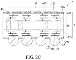
- FIG. 2C is a cross-sectional view of an electronic package of the first embodiment according to the present disclosure.
- FIGS. 3A to 3C are cross-sectional views illustrating a method for fabricating a semiconductor packaging substrate of a second embodiment according to the present disclosure
- FIG. 3A ′ is another aspect of FIG. 3A ;
- FIGS. 3C ′ and 3 C′′ are other aspects of FIG. 3C ;
- FIG. 3D is a cross-sectional view of an electronic package of the second embodiment according to the present disclosure.
- FIG. 3D ′ is another aspect of FIG. 3D .
- FIGS. 2A and 2B are cross-sectional views illustrating a method for fabricating a semiconductor packaging substrate 2 of a first embodiment according to the present disclosure.
- a circuit structure 2 a is provided.
- the circuit structure 2 a comprises a first side 20 a and a second side 20 b opposing the first side 20 a , onto both of which an electronic component (e.g., a semiconductor chip, a passive element, etc.) can be mounted.
- An externally connected side for a semiconductor chip to be mounted thereonto is called a chip-mounting side.
- the first side 20 a acts as the chip-mounting side.
- the circuit structure 2 a has a core layer 20 , in which a plurality of conductive portions 200 are formed.
- the core layer 20 is formed by a substrate composed of glass fiber and an organic resin, such as bismaleimide triazine (BT), FR4 and FR5.
- the core layer 20 is formed by a highly rigid organic substrate having a filler (e.g., SiO2), without glass fiber.
- a via forming process such as a mechanically drilling process and a laser drilling process, is performed on the core layer 20 to form a hole, and a conductive material is formed in the hole.
- the core layer 20 is formed of an organic insulating material, such as Ajinomoto build-up film (ABF), prepreg with or without glass fiber, and molding compound, such as epoxy molding compound (EMC).
- ABS Ajinomoto build-up film
- EMC epoxy molding compound
- the conductive portions 200 can be constituted by a single conductive pillar or a plurality of conductive pillars stacked on one another.
- the circuit structure 2 a comprises a built-up portion 21 disposed on the core layer 20 .
- the built-up portion 21 comprises at least one dielectric layer 210 and a plurality of circuit layers 211 bonded to the dielectric layer 210 .
- the dielectric layer 210 is a liquid epoxy resin, an ABF film, a prepreg, EMC or a photosensitive resin.
- the number of the circuit layers 211 can be adjusted on demands.
- solder resist structures 22 a and 22 b are made of graphene, solder resist, solder mask, ABF, non-photosensitive dielectric material (e.g., EMC) or other suitable materials.
- the core layer 20 is a silicon substrate, the built-up portion 21 is disposed on the silicon substrate, and the circuit structure 2 a becomes a silicon interposer.
- the circuit structure 2 a is in the form of a coreless layer.
- solder stands 23 are formed on the solder pads 212 on the second side 20 b of the circuit structure 2 a and on the hole walls of the holes 220 of the solder resist structure 22 b.
- the solder stands 23 and the solder pads 212 are made of the same material, such as copper.
- copper is electroplated on the exposed surface of the solder pads 212 of the circuit layer 211 and extends onto the hole walls of the holes 220 .
- At least one electronic component 40 is disposed on the exposed solder pads 212 on the first side 20 a of the circuit structure 2 a , an encapsulating layer 41 is formed on the first side 20 a of the circuit structure 2 a and bonded to the electronic component 40 , and a conductive element 42 , such as a solder tin ball, is mounted onto the solder stand 23 on the second side 20 b of the circuit structure 2 a , for a circuit board (not shown) to be bonded thereto.
- a conductive element 42 such as a solder tin ball
- the electronic component 40 is an active element, such as a semiconductor chip, a passive element, such as a resistor, a capacitor or an inductor, or a combination thereof.
- the electronic component 40 is a semiconductor chip, and is electrically connected to the solder pads 212 via a plurality of conductive bumps 400 containing solder tin in a flip-chip manner.
- the electronic component 40 is electrically connected to the solder pads 212 via a plurality of solder wires (not shown) in a wire bonding manner.
- the electronic component 40 can be electrically connected to the semiconductor packaging substrate 2 in other manners.
- the electronic component 40 is disposed on the second side 20 b of the circuit structure 2 a or embedded in the built-up portion 21 .
- the encapsulating layer 41 is an underfill, and is formed between the first side 20 a of the circuit structure 2 a and the electronic component 40 to encapsulate the conductive bumps 400 .
- the encapsulating layer 41 is a thin film used in a compressing process, an encapsulating resin used in a molding process, or a resin material used in a printing process to encapsulate the electronic component 40 and the conductive bumps 400 .
- the encapsulating layer 41 is formed by polyimide (PI), epoxy resin, or a packaging material for mold sealing.
- PI polyimide
- the electronic component 40 can be packaged in other manners.
- the conductive element 42 is formed on the solder stands 23 .
- the conductive element 42 comprises a solder tin material, such as a solder tin ball.
- a copper layer i.e., the solder stands 23
- the solder pads 212 is electroplated on the solder pads 212 on the ball planting side (the second side 20 b of the circuit structure 2 a ) and on the hole walls of the holes 220 of the solder resist structure 22 b .
- the conductive element 42 (a solder tin ball) will be in contact with the bottom surface and lateral wall of the solder stand 23 , a metal contact area between the conductive element 42 and the solder stand 23 is increased, and the bonding force between the conductive element 42 (a solder tin ball) and the solder stand 23 is increased.
- the present disclosure ensures that the conductive element 42 will not be broken or fell off from the solder stand 23 .
- FIGS. 3A to 3C are cross-sectional views illustrating a method for fabricating a semiconductor packaging substrate 3 of a second embodiment according to the present disclosure.
- the second embodiment differs from the first embodiment in the solder resist structure, which will be described in the following paragraphs.
- a metal support layer 33 is bonded via a bonding material 34 to the second side 20 b of the circuit structure 2 a , a plurality of first holes 330 are formed on the metal support layer 33 and extend through the bonding material 34 , and the solder pads 212 are exposed from the first holes 330 .
- An insulating layer 32 is formed on the solder pads 212 and the metal support layer 33 and in the first holes 330 .
- the metal support layer 33 is a steel plate or a nickel alloy (an alloy 42 ) piece
- the bonding material 34 is an adhesive resin
- the insulating layer 32 is made of graphene, solder resist, solder mask, ABF, non-photosensitive dielectric material (e.g., EMC), or other suitable materials.
- the insulating layer 32 is formed along the lateral walls of the first holes 330 . In another embodiment, the insulating layer 32 fills the first holes 330 completely, as shown in FIG. 3A ′.
- the insulating layer 32 is also formed on the first side 20 a of the circuit structure 2 a.
- a plurality of second holes 320 are formed on the insulating layer 32 on the second side 20 b of the circuit structure 2 a , the solder pads 212 are exposed from the second holes 320 , the insulating layer 32 and the metal support layer 33 act as the solder resist structure 32 a , and the insulating layer 32 encapsulates the metal support layer 33 .
- the solder stands 36 are formed on the solder pads 212 on the second side 20 b of the circuit structure 2 a and on the hole walls of the second holes 320 of the solder resist structure 32 b , to increase bonding contact area with the conductive element 42 and the bonding force therebetween.
- a conductively connecting block 37 is further formed on the cup-shaped solder stand 36 on demands.
- the conductively connecting block 37 is made of tin or other metal. As shown in FIG. 3C ′, a solder tin ball less than the second holes 320 in volume is mounted onto the cup-shaped solder stand 36 to form the conductively connecting block 37 . Therefore, the size of the conductive element 42 subsequently mounted is decreased effectively (referring to FIG. 3D ) to meet the requirement of fine spacing package.
- a bump bottom portion 361 ′ having an appropriate thickness is electroplated on the solder pads 212 in the second holes 320 , and extends to the remaining hole walls of the second holes 320 , thereby forming a cup-shaped solder stand 36 ′ having the bump bottom portion 361 ′ (which is made of the same material as the circuit layer 211 and the solder pads 212 , e.g., copper). Therefore, the size of the conductive element 42 subsequently mounted can be reduced effectively (referring to FIG. 3D ′), the requirement of a fine spacing package can be met, and the electric quality can be further optimized (by replacing a portion of the conductive element 42 made of tin with the bump bottom portion 361 ′ made of copper having good electric quality).
- the electronic package 4 ′ shown in FIG. 3D will be formed.
- the electronic component 40 is disposed on the exposed solder pads 212 on the first side 20 a of the circuit structure 2 a , the encapsulating layer 41 is formed on the first side 20 a and bonded to the electronic component 40 , and the conductive elements 42 are mounted on the solder stands 36 having the conductively connecting block 37 on the second side 20 b of the semiconductor packaging substrate 3 .
- the semiconductor packaging substrate 3 of FIG. 3C ′′ is adopted, the electronic package 4 ′′ shown in FIG. 3D ′ will be formed.
- the conductive elements 42 are mounted on the solder stand 36 ′ having the bump bottom portion 361 ′.
- a copper layer i.e., forming the cup-shaped solder stands 36 and 36 ′
- a copper layer is electroplated on the solder pads 212 on the ball planting side (the second side 20 b of the circuit structure 2 a ) and the hole walls of the second holes 320 of the solder resist structure 32 b , allowing the conductive element 42 (a solder tin ball) to be in contact with the bottom surface and lateral wall of the solder stands 36 and 36 ′ during the subsequent ball planting process, to thereby increase the metal contact area and the bonding force between the conductive element 42 (solder tin ball) and the solder stands 36 and 36 ′.
- the present disclosure increases the bonding force between the conductive element 42 and the solder stands 36 and 36 ′, and ensures that the conductive element 42 will not be broken or fell off from the solder stands 36 and 36 ′.
- the installation of the metal support layer 33 on the second side 20 b of the circuit structure 2 a improves the rigidity of the semiconductor packaging substrate 3 .
- the semiconductor packaging substrate 3 according to the present disclosure when applied to a large-sized package, can still have high enough rigidity, even if being thinned. Therefore, during the subsequent high temperature process or the use of the product, the electronic package 4 ′, 4 ′′ does not suffer from warpage, and can be well connected with the electronic component 40 or the circuit board.
- the circuit structure 2 a may have warpage to any extent.
- the rigidity of the semiconductor packaging substrate 3 can be controlled by adjusting the thickness of the metal support layer 33 or by the material of the metal support layer 33 . Therefore, the core layer 20 needs not be thickened, but can be thinned, or be omitted, and the warpage problem of the semiconductor packaging substrate 3 can still be solved.
- the size and material of the conductive element 42 can be reduced effectively, the requirement of a fine spacing package can be met, and the electric quality of the semiconductor packaging substrate 3 can be optimized (by replacing a portion of the conductive element 42 made of tin with the bump bottom portion 361 ′ made of copper having good electric quality).
- the design of the solder stands 23 , 36 and 36 ′ increase the contact area of the conductive element 42 with metal, and increase the bonding force between the conductive element 42 (solder tin ball) and the solder stands 23 , 36 and 36 ′. Therefore, the present disclosure can prevent the conductive element 42 from being broken or fell off from the solder stands 23 , 36 and 36 ′.
Landscapes
- Engineering & Computer Science (AREA)
- Physics & Mathematics (AREA)
- Condensed Matter Physics & Semiconductors (AREA)
- General Physics & Mathematics (AREA)
- Computer Hardware Design (AREA)
- Microelectronics & Electronic Packaging (AREA)
- Power Engineering (AREA)
- Electric Connection Of Electric Components To Printed Circuits (AREA)
- Ceramic Engineering (AREA)
- Manufacturing & Machinery (AREA)
- Geometry (AREA)
- Wire Bonding (AREA)
Abstract
Description
Claims (10)
Applications Claiming Priority (2)
| Application Number | Priority Date | Filing Date | Title |
|---|---|---|---|
| TW108110749 | 2019-03-27 | ||
| TW108110749A TWI762777B (en) | 2019-03-27 | 2019-03-27 | Semiconductor package substrate and manufacturing method thereof and electronic package and manufacturing method thereof |
Publications (2)
| Publication Number | Publication Date |
|---|---|
| US20200312756A1 US20200312756A1 (en) | 2020-10-01 |
| US11335630B2 true US11335630B2 (en) | 2022-05-17 |
Family
ID=72604696
Family Applications (1)
| Application Number | Title | Priority Date | Filing Date |
|---|---|---|---|
| US16/832,084 Active US11335630B2 (en) | 2019-03-27 | 2020-03-27 | Semiconductor package substrate, electronic package and methods for fabricating the same |
Country Status (2)
| Country | Link |
|---|---|
| US (1) | US11335630B2 (en) |
| TW (1) | TWI762777B (en) |
Families Citing this family (1)
| Publication number | Priority date | Publication date | Assignee | Title |
|---|---|---|---|---|
| TWI759120B (en) * | 2021-03-04 | 2022-03-21 | 恆勁科技股份有限公司 | Intermediate substrate and manufacturing method thereof |
Citations (4)
| Publication number | Priority date | Publication date | Assignee | Title |
|---|---|---|---|---|
| US6930032B2 (en) * | 2002-05-14 | 2005-08-16 | Freescale Semiconductor, Inc. | Under bump metallurgy structural design for high reliability bumped packages |
| US7875805B2 (en) * | 2007-03-02 | 2011-01-25 | Unimicron Technology Corp. | Warpage-proof circuit board structure |
| US7968446B2 (en) * | 2008-10-06 | 2011-06-28 | Wan-Ling Yu | Metallic bump structure without under bump metallurgy and manufacturing method thereof |
| US8058568B2 (en) * | 2007-08-08 | 2011-11-15 | Unimicron Technology Corp. | Circuit board and method for fabricating the same |
Family Cites Families (6)
| Publication number | Priority date | Publication date | Assignee | Title |
|---|---|---|---|---|
| TWI368302B (en) * | 2006-09-19 | 2012-07-11 | Surface structure of package substrate and method of manufacturing the same | |
| TWI418269B (en) * | 2010-12-14 | 2013-12-01 | 欣興電子股份有限公司 | Package substrate with embedded perforation interposer and preparation method thereof |
| TWI483360B (en) * | 2011-12-08 | 2015-05-01 | Unimicron Technology Corp | Method for manufacturing package substrate |
| TWI424545B (en) * | 2011-12-08 | 2014-01-21 | 欣興電子股份有限公司 | Method of manufacturing package substrate |
| TWM462947U (en) * | 2012-06-08 | 2013-10-01 | Unimicron Technology Corp | Package substrate |
| CN103906370B (en) * | 2012-12-27 | 2017-01-11 | 碁鼎科技秦皇岛有限公司 | Chip packaging structure, circuit board having embedded component and manufacturing method thereof |
-
2019
- 2019-03-27 TW TW108110749A patent/TWI762777B/en active
-
2020
- 2020-03-27 US US16/832,084 patent/US11335630B2/en active Active
Patent Citations (4)
| Publication number | Priority date | Publication date | Assignee | Title |
|---|---|---|---|---|
| US6930032B2 (en) * | 2002-05-14 | 2005-08-16 | Freescale Semiconductor, Inc. | Under bump metallurgy structural design for high reliability bumped packages |
| US7875805B2 (en) * | 2007-03-02 | 2011-01-25 | Unimicron Technology Corp. | Warpage-proof circuit board structure |
| US8058568B2 (en) * | 2007-08-08 | 2011-11-15 | Unimicron Technology Corp. | Circuit board and method for fabricating the same |
| US7968446B2 (en) * | 2008-10-06 | 2011-06-28 | Wan-Ling Yu | Metallic bump structure without under bump metallurgy and manufacturing method thereof |
Also Published As
| Publication number | Publication date |
|---|---|
| TWI762777B (en) | 2022-05-01 |
| TW202036821A (en) | 2020-10-01 |
| US20200312756A1 (en) | 2020-10-01 |
Similar Documents
| Publication | Publication Date | Title |
|---|---|---|
| US12362263B2 (en) | Electronic package and method of fabricating the same | |
| US11508639B2 (en) | System in package (SiP) semiconductor package | |
| US10410968B2 (en) | Semiconductor package and method of manufacturing the same | |
| EP2798675B1 (en) | Method for a substrate core layer | |
| US8067832B2 (en) | Embedded integrated circuit package system and method of manufacture thereof | |
| US8580608B2 (en) | Fabrication method of package structure having embedded semiconductor component | |
| US11183447B2 (en) | Flip-chip package substrate and method for fabricating the same | |
| US12255182B2 (en) | Electronic package and manufacturing method thereof | |
| US11450597B2 (en) | Semiconductor package substrate having heat dissipating metal sheet on solder pads, method for fabricating the same, and electronic package having the same | |
| US20070020812A1 (en) | Circuit board structure integrated with semiconductor chip and method of fabricating the same | |
| CN111755409A (en) | Semiconductor packaging substrate and its manufacturing method and electronic package and its manufacturing method | |
| US11335630B2 (en) | Semiconductor package substrate, electronic package and methods for fabricating the same | |
| US20160104652A1 (en) | Package structure and method of fabricating the same | |
| US10515883B2 (en) | 3D system-level packaging methods and structures | |
| US12255165B2 (en) | Electronic package and carrier thereof and method for manufacturing the same | |
| US20240243048A1 (en) | Electronic package, package substrate and manufacturing method thereof | |
| US20250336739A1 (en) | Electronic package and manufacturing method thereof | |
| US20110101510A1 (en) | Board on chip package substrate and manufacturing method thereof | |
| US11903145B2 (en) | Wiring board and semiconductor module including the same | |
| US20240096721A1 (en) | Electronic package and manufacturing method thereof | |
| KR20240164225A (en) | Semiconductor package | |
| KR20240171423A (en) | Semiconductor package | |
| KR20240164247A (en) | Semiconductor package | |
| KR20240164743A (en) | Semiconductor device and method of making a dual-side molded system-in-package with fine-pitched interconnects | |
| TW202403995A (en) | Semiconductor device and method of forming thin heat sink using e-bar substrate |
Legal Events
| Date | Code | Title | Description |
|---|---|---|---|
| AS | Assignment |
Owner name: PHOENIX PIONEER TECHNOLOGY CO., LTD., TAIWAN Free format text: ASSIGNMENT OF ASSIGNORS INTEREST;ASSIGNORS:CHOU, PAO-HUNG;YU, CHUN-HSIEN;HSU, SHIH-PING;REEL/FRAME:052243/0035 Effective date: 20200316 |
|
| FEPP | Fee payment procedure |
Free format text: ENTITY STATUS SET TO UNDISCOUNTED (ORIGINAL EVENT CODE: BIG.); ENTITY STATUS OF PATENT OWNER: SMALL ENTITY |
|
| FEPP | Fee payment procedure |
Free format text: ENTITY STATUS SET TO SMALL (ORIGINAL EVENT CODE: SMAL); ENTITY STATUS OF PATENT OWNER: SMALL ENTITY |
|
| STPP | Information on status: patent application and granting procedure in general |
Free format text: DOCKETED NEW CASE - READY FOR EXAMINATION |
|
| STPP | Information on status: patent application and granting procedure in general |
Free format text: NON FINAL ACTION MAILED |
|
| STPP | Information on status: patent application and granting procedure in general |
Free format text: RESPONSE TO NON-FINAL OFFICE ACTION ENTERED AND FORWARDED TO EXAMINER |
|
| STPP | Information on status: patent application and granting procedure in general |
Free format text: NOTICE OF ALLOWANCE MAILED -- APPLICATION RECEIVED IN OFFICE OF PUBLICATIONS |
|
| STPP | Information on status: patent application and granting procedure in general |
Free format text: PUBLICATIONS -- ISSUE FEE PAYMENT VERIFIED |
|
| STCF | Information on status: patent grant |
Free format text: PATENTED CASE |
|
| MAFP | Maintenance fee payment |
Free format text: PAYMENT OF MAINTENANCE FEE, 4TH YR, SMALL ENTITY (ORIGINAL EVENT CODE: M2551); ENTITY STATUS OF PATENT OWNER: SMALL ENTITY Year of fee payment: 4 |