US11326255B2 - ALD reactor for coating porous substrates - Google Patents
ALD reactor for coating porous substrates Download PDFInfo
- Publication number
- US11326255B2 US11326255B2 US14/175,396 US201414175396A US11326255B2 US 11326255 B2 US11326255 B2 US 11326255B2 US 201414175396 A US201414175396 A US 201414175396A US 11326255 B2 US11326255 B2 US 11326255B2
- Authority
- US
- United States
- Prior art keywords
- showerhead
- plate
- substrate
- showerhead plate
- holes
- Prior art date
- Legal status (The legal status is an assumption and is not a legal conclusion. Google has not performed a legal analysis and makes no representation as to the accuracy of the status listed.)
- Active, expires
Links
Images


Classifications
-
- C—CHEMISTRY; METALLURGY
- C23—COATING METALLIC MATERIAL; COATING MATERIAL WITH METALLIC MATERIAL; CHEMICAL SURFACE TREATMENT; DIFFUSION TREATMENT OF METALLIC MATERIAL; COATING BY VACUUM EVAPORATION, BY SPUTTERING, BY ION IMPLANTATION OR BY CHEMICAL VAPOUR DEPOSITION, IN GENERAL; INHIBITING CORROSION OF METALLIC MATERIAL OR INCRUSTATION IN GENERAL
- C23C—COATING METALLIC MATERIAL; COATING MATERIAL WITH METALLIC MATERIAL; SURFACE TREATMENT OF METALLIC MATERIAL BY DIFFUSION INTO THE SURFACE, BY CHEMICAL CONVERSION OR SUBSTITUTION; COATING BY VACUUM EVAPORATION, BY SPUTTERING, BY ION IMPLANTATION OR BY CHEMICAL VAPOUR DEPOSITION, IN GENERAL
- C23C16/00—Chemical coating by decomposition of gaseous compounds, without leaving reaction products of surface material in the coating, i.e. chemical vapour deposition [CVD] processes
- C23C16/44—Chemical coating by decomposition of gaseous compounds, without leaving reaction products of surface material in the coating, i.e. chemical vapour deposition [CVD] processes characterised by the method of coating
- C23C16/455—Chemical coating by decomposition of gaseous compounds, without leaving reaction products of surface material in the coating, i.e. chemical vapour deposition [CVD] processes characterised by the method of coating characterised by the method used for introducing gases into reaction chamber or for modifying gas flows in reaction chamber
- C23C16/45563—Gas nozzles
- C23C16/45565—Shower nozzles
-
- C—CHEMISTRY; METALLURGY
- C04—CEMENTS; CONCRETE; ARTIFICIAL STONE; CERAMICS; REFRACTORIES
- C04B—LIME, MAGNESIA; SLAG; CEMENTS; COMPOSITIONS THEREOF, e.g. MORTARS, CONCRETE OR LIKE BUILDING MATERIALS; ARTIFICIAL STONE; CERAMICS; REFRACTORIES; TREATMENT OF NATURAL STONE
- C04B38/00—Porous mortars, concrete, artificial stone or ceramic ware; Preparation thereof
- C04B38/0093—Other features
- C04B38/0096—Pores with coated inner walls
-
- C—CHEMISTRY; METALLURGY
- C23—COATING METALLIC MATERIAL; COATING MATERIAL WITH METALLIC MATERIAL; CHEMICAL SURFACE TREATMENT; DIFFUSION TREATMENT OF METALLIC MATERIAL; COATING BY VACUUM EVAPORATION, BY SPUTTERING, BY ION IMPLANTATION OR BY CHEMICAL VAPOUR DEPOSITION, IN GENERAL; INHIBITING CORROSION OF METALLIC MATERIAL OR INCRUSTATION IN GENERAL
- C23C—COATING METALLIC MATERIAL; COATING MATERIAL WITH METALLIC MATERIAL; SURFACE TREATMENT OF METALLIC MATERIAL BY DIFFUSION INTO THE SURFACE, BY CHEMICAL CONVERSION OR SUBSTITUTION; COATING BY VACUUM EVAPORATION, BY SPUTTERING, BY ION IMPLANTATION OR BY CHEMICAL VAPOUR DEPOSITION, IN GENERAL
- C23C16/00—Chemical coating by decomposition of gaseous compounds, without leaving reaction products of surface material in the coating, i.e. chemical vapour deposition [CVD] processes
- C23C16/04—Coating on selected surface areas, e.g. using masks
- C23C16/045—Coating cavities or hollow spaces, e.g. interior of tubes; Infiltration of porous substrates
-
- C—CHEMISTRY; METALLURGY
- C23—COATING METALLIC MATERIAL; COATING MATERIAL WITH METALLIC MATERIAL; CHEMICAL SURFACE TREATMENT; DIFFUSION TREATMENT OF METALLIC MATERIAL; COATING BY VACUUM EVAPORATION, BY SPUTTERING, BY ION IMPLANTATION OR BY CHEMICAL VAPOUR DEPOSITION, IN GENERAL; INHIBITING CORROSION OF METALLIC MATERIAL OR INCRUSTATION IN GENERAL
- C23C—COATING METALLIC MATERIAL; COATING MATERIAL WITH METALLIC MATERIAL; SURFACE TREATMENT OF METALLIC MATERIAL BY DIFFUSION INTO THE SURFACE, BY CHEMICAL CONVERSION OR SUBSTITUTION; COATING BY VACUUM EVAPORATION, BY SPUTTERING, BY ION IMPLANTATION OR BY CHEMICAL VAPOUR DEPOSITION, IN GENERAL
- C23C16/00—Chemical coating by decomposition of gaseous compounds, without leaving reaction products of surface material in the coating, i.e. chemical vapour deposition [CVD] processes
- C23C16/44—Chemical coating by decomposition of gaseous compounds, without leaving reaction products of surface material in the coating, i.e. chemical vapour deposition [CVD] processes characterised by the method of coating
- C23C16/455—Chemical coating by decomposition of gaseous compounds, without leaving reaction products of surface material in the coating, i.e. chemical vapour deposition [CVD] processes characterised by the method of coating characterised by the method used for introducing gases into reaction chamber or for modifying gas flows in reaction chamber
- C23C16/45523—Pulsed gas flow or change of composition over time
- C23C16/45525—Atomic layer deposition [ALD]
- C23C16/45544—Atomic layer deposition [ALD] characterized by the apparatus
-
- H—ELECTRICITY
- H01—ELECTRIC ELEMENTS
- H01J—ELECTRIC DISCHARGE TUBES OR DISCHARGE LAMPS
- H01J43/00—Secondary-emission tubes; Electron-multiplier tubes
- H01J43/04—Electron multipliers
- H01J43/06—Electrode arrangements
- H01J43/18—Electrode arrangements using essentially more than one dynode
- H01J43/24—Dynodes having potential gradient along their surfaces
- H01J43/246—Microchannel plates [MCP]
-
- H—ELECTRICITY
- H01—ELECTRIC ELEMENTS
- H01J—ELECTRIC DISCHARGE TUBES OR DISCHARGE LAMPS
- H01J2231/00—Cathode ray tubes or electron beam tubes
- H01J2231/50—Imaging and conversion tubes
- H01J2231/501—Imaging and conversion tubes including multiplication stage
- H01J2231/5013—Imaging and conversion tubes including multiplication stage with secondary emission electrodes
- H01J2231/5016—Michrochannel plates [MCP]
Definitions
- This invention relates to an improved system and method for ALD/CVD deposition for coating porous substrates. More particularly, the invention relates to a system and method for coating porous substrates, such as capillary glass arrays, using an ALD reactor having a showerhead inlet section which provides a uniform flux of precursor reactants across a surface of the porous substrate, substrate fixturing to provide a flow-through geometry in which precursor reactants and carrier gas are forced to flow-through pores of the porous substrate, and a showerhead outlet section to ensure that the flow remains perpendicular to the porous substrate throughout the coating process, to minimize deposition nonuniformities and enhance the efficiency of precursor purging.
- ALD reactor having a showerhead inlet section which provides a uniform flux of precursor reactants across a surface of the porous substrate, substrate fixturing to provide a flow-through geometry in which precursor reactants and carrier gas are forced to flow-through pores of the porous substrate, and a showerhead outlet section to ensure that the flow remains perpendicular to the porous substrate throughout
- ALD atomic layer deposition
- the upstream portion of the substrate will always experience a larger precursor flux while the downstream portion of the substrate will experience a larger flux of the reaction byproducts.
- Non-idealities in the ALD process coupled with these non-uniform fluxes, can produce non-uniform hereinafter (“NU”) coatings along the flow axis.
- NU non-uniform hereinafter
- the non-uniform consumption of precursor across the surface of the substrate in the direction perpendicular to the flow can be another source of NU in cross-flow reactors.
- porous substrates molecules such as H 2 O which physisorb strongly to surfaces can continue to outgas for long periods of time.
- H 2 O precursor or the H 2 O is a reaction product in a porous substrate the H 2 O must diffuse out of the pore in order to become entrained in the purge gas. Because the purge gas flow is normal to the axis of the pores, there is a high probabliltiy that the H 2 O will diffuse back into a downstream pore and again physisorb.
- An improved ALD reactor for coating substrates, particularly porous substrates having an aspect ratio, defined as pore length divided by pore diameter, of greater than about 10-1000, and a high surface area by virtue of the porosity.
- the system includes at least a showerhead style structure for use as a precursor inlet to provide a uniform precursor flux across the entire surface of the substrate.
- the porous substrate is also preferably positioned relative to the showerhead structure in a fixture that forces a flow-through geometry wherein the precursor flux and a carrier gas are required to flow through the pores of the porous substrate.
- the flow-through reactor system includes a second showerhead style structure located downstream of the porous substrate to maintain a uniform flow that is everywhere parallel to the axis of the substrate pores.
- porous substrates can be disposed between the dual showerheads to enable deposition of material on multiple substrates.
- FIG. 1 a shows a top view schematic of a conventional ALD cross-flow reactor; and FIG. 1 b shows an elevation view of the reactor of FIG. 1 a;
- FIG. 2 a shows a commercial ALD reactor
- FIG. 2 b shows a view of a reaction chamber of the reactor of FIG. 2 a
- FIG. 2 c shows placement of a cross-flow reaction chamber suitable for 300 mm substrates in the reactor;
- FIG. 3 a shows an as received 8′′ ⁇ 8′′ capillary glass array mounted in a stainless steel frame
- FIG. 3 b shows the capillary glass array after ALD functionalization with a nanocomposite of Mo:Al 2 O 3 to produce a microchannel plate (MCP)
- FIG. 3 c shows a 33 mm diameter MCP after the same ALD functionalization in FIG. 3 b;
- FIG. 4 a shows the cross-flow reaction chamber of FIGS. 2 b and 2 c with a 300 mm Si wafer before Al 2 O 3 ALD deposition
- FIG. 4 b shows the 300 mm Si wafer after ALD deposition of an Al 2 O 3 coating with Trimethyl Aluminum (“TMA”) and water (H 2 O) vapour precursors;
- TMA Trimethyl Aluminum
- H 2 O water
- FIG. 5 shows a thickness contour plot of the ALD Al 2 O 3 coating across the 300 mm Si wafer after the ALD deposition of FIG. 4 b for 1000 ALD cycles of TMA-N 2 purge-H 2 O—N 2 purge;
- FIGS. 6 a -6 c show a cross-flow reaction chamber for the scale up of the ALD deposition process of FIG. 4 b with FIG. 6 a being an overview, FIG. 6 b a close-up of the inside view of the cross-flow reaction chamber and FIG. 6 c shows a 1′′ ⁇ 1′′ to 12′′ ⁇ 12′′ plane glass substrate with ITO (indium tin oxide) coating deposited by ALD in the cross-flow reaction chamber of FIGS. 6 a and 6 b;
- ITO indium tin oxide
- FIG. 7 shows a plot of resistivity measured at different locations across a 300 mm Si wafer for a Chem-2 (Mo—Al 2 O 3 ) coating done with the system of FIGS. 6 a - 6 c;
- FIG. 8 shows a photograph of a 300 mm Si wafer after Al 2 O 3 ALD performed in the presence of an 8′′ ⁇ 8′′ capillary glass array using the system of FIGS. 2 c and 4 a;
- FIG. 9 shows the thickness profiles, expressed as the growth rate versus the position across 300 mm wafers, following the ALD deposition of Al 2 O 3 in the cross-flow reaction chamber system of FIGS. 2 c and 4 a both with and without the presence of an 8′′ ⁇ 8′′ capillary glass array using a variety of deposition conditions;
- FIG. 10 shows the thickness profiles, expressed as the growth rate versus the position across 300 mm wafers, following the ALD deposition of MgO using bis-cyclopentadienyl magnesium (MgCp2) and H 2 O precursors in the cross-flow reaction chamber of system of FIGS. 2 c and 4 a in the presence of an 8′′ ⁇ 8′′ capillary glass array using a variety of deposition conditions.
- MgCp2 bis-cyclopentadienyl magnesium
- H 2 O precursors in the cross-flow reaction chamber of system of FIGS. 2 c and 4 a in the presence of an 8′′ ⁇ 8′′ capillary glass array using a variety of deposition conditions.
- the solid data points and line indicate the MgO growth rate measurements performed under identical conditions but with the capillary glass array removed;
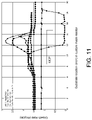
- FIG. 11 shows thickness trend for MgO ALD deposited without the capillary glass array (black dots) and with the capillary glass array (colored dots) using different Mg(Cp) 2 dose times performed using the cross-flow reaction chamber of FIGS. 6 a and 6 b.
- FIG. 12 shows Mo growth rate versus distance across a 300 mm Si wafer for Mo ALD deposited with and without the capillary glass array under different dose and purge times with deposition performed at 200° C. using MoF 6 and Si 2 H 6 precursors in the cross-flow reaction chamber of FIGS. 2 c and 4 a;
- FIG. 13 a shows a schematic side view of one embodiment of a through-flow (or flow-through) system for an ALD/CVD reactor with a single porous substrate
- FIG. 13 b shows a schematic side view of another embodiment of a through-flow system with multiple porous substrates;
- FIG. 14 a shows a side view cross section of the reactor of FIG. 13 a ; and FIG. 14 b shows a top view of the top showerhead portion of FIG. 14 a;
- FIG. 15 a shows a photograph of a flow-through reactor with dual showerheads; and FIG. 15 b shows another view of the embodiment of FIG. 15 a;
- FIG. 16 a shows Al 2 O 3 deposition profiles using various conditions (with and without capillary glass arrays) for the system of FIG. 13 a ;
- FIG. 16 b shows MgO deposition growth rate with the Si coupons placed below the MCP;
- FIG. 17 a shows thickness and refractive index of W:Al 2 O 3 , (chem-1) on Si (100) coupons using the system of FIG. 13 a with deposition for an 8′′ ⁇ 8′′ capillary glass array disposed on top at 150° C. using WF 6 and Si 2 H 6 for W and with TMA and H 2 O for Al 2 O 3 ;
- FIG. 17 b shows further results for deposition of W:Al 2 O 3 , (chem-1) on an 8′′ ⁇ 8′′ MCP (no Si) using the system of FIG. 13 a ;
- FIG. 17 c shows X-ray fluorescence analysis of the relative W concentration from front and back sides of the MCP versus location on the MCP, deposited uniformly and done at 150° C. using WF 6 and Si 2 H 6 for W and TMA and H 2 O for Al 2 O 3 .
- FIGS. 18A-B illustrate one embodiment of a 8′′ ⁇ 8′′ porous capillary glass array substrate (MCP) placement inside the dual showerhead ALD reaction chamber: FIG. 18A MCP placed on bottom showerhead elevated with ceramic beads (side view); FIG. 18B MCP placement with monitor Si witness coupons on the bottom showerhead (view from top)
- MCP capillary glass array substrate
- FIGS. 19A-B illustrate one embodiment of a 8′′ ⁇ 8′′ porous capillary glass array substrate (MCP) placement with side pieces of similar porous substrate inside the dual showerhead ALD reaction chamber (monitor silicon pieces are positioned below the MCP);
- FIG. 19A illustrates a MCP substrate holder with side cut pieces of similar type of MCP;
- FIG. 19B illustrates a MCP placed with side pieces (view from top).
- MCP capillary glass array substrate
- FIG. 20A Growth rate of Al 2 O 3 with and without side pieces of MCP in the dual showerhead ALD reaction chamber during coating of 8′′ ⁇ 8′′ MCP for different reaction chamber configurations;
- FIG. 20B Growth rate of Al 2 O 3 with side pieces of similar MCP in the dual showerhead ALD reaction chamber;
- FIG. 20C illustrates measurement of the growth rate of Al 2 O 3 along the diagonal of the 8′′ ⁇ 8′′ MCP with side pieces of similar type of MCP in the dual showerhead ALD reaction chamber.
- FIG. 21 illustrates a 8′′ ⁇ 8′′ porous capillary glass array substrate (MCP) with side pieces of similar type of MCP cut to surround the 8′′ ⁇ 8′′ MCP.
- MCP capillary glass array substrate
- FIG. 22 illustrates growth rate of Al 2 O 3 with side pieces of similar MCP in the dual showerhead ALD reaction chamber configured as in FIG. 21 .
- Prior art systems consist of an ALD cross-flow reactor 10 wherein a precursor and carrier are input through precursor inlets 20 disposed within a flow distributor plate 30 .
- the reactor 10 further includes a precursor distributor 40 , a precursor outlet 50 disposed within a second flow distributor plate 60 and a planar substrate 70 .
- precursor/carrier gas 110 flows from the precursor inlets 20 , flow across the planar substrate 70 , and out the precursor outlet 50 .
- example data from performance of this conventional prior art reactor 10 show how such systems suffer from a number of deficiencies, including irregular layer thickness across the substrate.
- FIGS. 2 a -2 c illustrate various views of a commercial Beneq ALD deposition system 11 .
- a chamber 185 has subchamber 190 for carrying out conventional cross-flow ALD deposition.
- certain ALD functionalities can be performed, such as the scale-up of substrate size for 33 mm MCP disks 170 (see FIG. 3 c ) up to 300 mm MCP.
- FIG. 3 a shows an 8′′ ⁇ 8:capillary glass array (MCP) 200 before deposition and FIG. 3 b after ALD functionalization with a nanocomposite of Mo:Al 2 O 3 layer 210 and FIG.
- MCP capillary glass array
- FIGS. 4 a and 4 b show photographs of 300 mm silicon wafer 201 and 211 before and after ALD functionalization in the subchamber 190 (see FIG. 4 a ).
- FIG. 5 shows a schematic of precursor input and output with a topograph of Al 2 O 3 layer thickness across the 300 mm Si wafer 211 after ALD deposition for 1000 cycles.
- the referenced Si wafer is for monitoring the reaction and providing a compariable between embodiments with the MCP installed and without the MCP installed.
- the layer thickness is uniform on the 300 mm Si wafer coated in the cross-flow reactor without the MCP installed as evidenced by the coating thickness variation of ⁇ 1% across the wafer.
- FIGS. 6 a -6 c show a scale-up of a conventional reactor with FIG. 6 a being a photograph of a closed cross-flow reaction chamber 230 for depositing an ALD coating on substrates with up to 12′′ ⁇ 18′′ dimensions.
- FIG. 6 b shows an inside view of the cross-flow reaction chamber 230 .
- FIG. 6 c shows photographs of a 1′′ ⁇ 1′′ scale-up to a 12′′ ⁇ 12′′ glass substrate with an ALD indium tin oxide coating that is uniform in thickness within 5%.
- the ITO coatings on these planar substrates 240 and 250 are very uniform in thickness in the absence of a porous substrate
- the system of FIGS. 2 c and 4 a was used to carry out the ALD cross-flow deposition.
- the resistivity of the chem-2 coatings are extremely sensitive to the composition of the film, with the resistivity decreasing exponentially with increasing Mo content.
- the very uniform resistivity of the chem-2 film across the 300 mm Si wafer is evidence that the composition of the chem-2 coatings is very uniform in the conventional cross-flow reactor without the MCP installed.
- FIG. 8 shows a photograph of a 300 mm Si (100) wafer after Al 2 O 3 deposition with a capillary glass array substrate (MCP) placed in close proximity to the wafer (note the precursor inlet and outlet) throughout the coating process.
- MCP capillary glass array substrate
- the thickness of the coating was measured at various points by spectroscopic ellipsometry, and the thickness values are indicated on FIG. 8 .
- the data shows substantial non-uniformity of the ALD coating.
- the coating thickness varies by 300% (from 50 nm to 150 nm) with the MCP installed, in comparison to the ⁇ 1% thickness variation obtained in the absence of the MCP as shown in FIG. 5 .
- These depositions were performed at 200C using (Trimethyl Aluminum) “TMA” and H 2 O precursor.
- FIG. 9 shows detailed plots of ALD Al 2 O 3 layer growth rate versus distance across 300 mm Si wafer substrates coated using the cross-flow system of FIGS. 2 c and 4 a.
- the plot labeled 1421x3-5-1 FR has no capillary glass array substrate (MCP) installed, whereas all others do.
- MCP capillary glass array substrate
- Deposition conditions were as for FIG. 8 .
- the presence of the MCP resulted in highly non-uniform layer thickness across the Si wafer, regardless of the many changes in process conditions made in an effort to obtain a uniform layer thickness.
- the MCP is referenced as an example, similar porous substrates will produce the same non-uniform coatings, for instance substrates manufactured by sintering glass beads.
- porous substrates may be comprised of aerogels, xerogels, microfiber plates, nanotube-based mesh or cloth, and 3D-printed materials. Further, the holes need not be a regular array of holes, in certain embodiments the array will be irregular and the pores will be tortuous. These porous substrates may be intended for use in catalysis, separations, or electron multipliers.
- FIG. 10 shows growth rate versus location on a Si wafer for MgO coatings prepared by ALD with and without an MCP installed, and deposited using MgCp 2 and H 2 O precursors with precursor inlet located on the left side at location “0”.
- depositions used the cross-flow system of FIGS. 2 c and 4 a.
- the conditions were varied in an attempt to obtain a uniform MgO coating with the MCP installed. For instance, deposition was performed with flow restrictors installed, precursor was supplied under both flow-boost conditions and constant N 2 flow conditions.
- the baseline trace shows the MgO thickness without the MCP installed. Again, the MgO layer thickness is highly non-uniform with the MCP installed, as for the Al 2 O 3 in FIG.
- FIG. 11 likewise shows non-uniform thickness for MgO deposition using the reactor system in FIGS. 6 a and 6 b with the MCP substrate installed, regardless of process conditions, whereas the thickness is uniform in the absence of the MCP.
- FIG. 12 is shows the variation in Mo growth rate across a 300 mm Si wafer using the cross-flow system of FIGS. 2 c and 4 a .
- the thickness is highly non-uniform for ALD performed with the MCP substrate installed regardless of process conditions. But again, the Mo thickness is uniform in the absence of the MCP. Depositions were carried out at 200C using MoF 6 and Si 2 H 6 precursors.
- a dual showerhead flow-through reactor 120 includes a top showerhead (or first plate) 130 , a porous substrate 145 , a bottom showerhead (or second plate) 140 with a central precursor injection port 150 for a precursor and the carrier gas 110 .
- the top showerhead 130 and bottom showerhead 140 can be made out of any metal, alloy, or ceramic compatible with the process temperatures and chemical precursors for the intended ALD or CVD growth.
- Each of the top shower head 130 and bottom shower head 140 have a plurality of holes. The hole size and the density of the holes is selected for the desired delivery of the precursor flux.
- the top showerhead 130 includes smaller diameter holes than the bottom shower head 140 .
- the ratio of the hole diameters between the top showerhead 130 and the bottom showerhead 140 can be adjusted to adjust the relative conductance. Likewise the overall thickness of the holes (the showerhead thickness) for the showerheads 130 , 140 dictates the conductance of the holes.
- the top showerhead 130 and the bottom showerhead 140 are sealed to or integral with a side of the reactor 120 such that precursor cannot flow “around” the shower head but must flow-through the showerhead 130 , 140 .
- the precursor injection portion 150 is preferably spaced sufficiently from the top showerhead 130 to allow for uniform distribution of the precursor with respect to the top showerhead 130 prior to passing through the holes in the showerhead.
- the precursor supply arrangement comprised of the precursor injection 150 , the precursors 120 , and the inert purge gas 110 can be connected only above the top showerhead 130 as shown in FIG. 13 a , or can be connected both above the top showerhead 130 and below the bottom showerheads 140 .
- the exhaust portion 155 can be connected only below the bottom showerhead 140 as shown in FIG. 13 a , or can be connected both below the bottom showerhead 140 and above the top showerhead 130 .
- the reactor 120 further includes showerhead spacers 160 separating the top showerhead 130 and the bottom showerhead 140 and an exhaust port 155 .
- the spacers provide a spacing of up to 3-5 mm.
- the showerhead spacers are preferably positioned about the periphery to allow an internal space defined by the showerhead spacers and the top showerhead 130 and bottom showerhead 140 in which the MCP 145 can be placed.
- the MCP 145 is positioned on ceramic supports 180 (see FIG. 15 b ) and also disposed between the top showerhead 130 and the bottom showerhead 140 .
- the exhaust port 155 is in communication with a pump to assist in evacuating the reactor and in moving the precursor through the showheads 130 , 140 .
- a conical output section 185 of the reactor 120 provides improved pumping.
- a plurality of flow-through substrates 145 can be used in the flow-through reactor 120 .
- the gap between the top showerhead 130 and the porous substrate 145 (G) should be minimized to ensure that the carrier gas sweep is effective, and that the overall residence time of the precursors in the showerhead reactor is short.
- the gap between the precursor inlet tube 155 and the top showerhead 130 (H) should be minimized to reduce the overall residence time of the precursors in the showerhead reactor.
- FIGS. 14 a and 14 b Further details of the reactor 120 are shown in FIGS. 14 a and 14 b .
- the top view of the top showerhead 130 there is a matrix of through holes 185 which enable controlled flow-through of the precursor/carrier gas 155 to impact on the intervening MCP 145 for deposition of material.
- FIGS. 16 a and 16 b are shown example data with FIG. 16 a showing ALD deposition of Al 2 O 3 , with and without the MCP 145 .
- FIG. 16 b shows MgO ALD deposition under various conditions with and without MCP 145 .
- FIG. 17 a -17 c further show ALD deposition of W:Al 2 O 3 (Chem-1) with various system features with and without MCP 145 .
- FIG. 17 a shows thickness and refractive index of W:Al 2 O 3 , on Si (100) using the system of FIGS. 15 a , 15 b with deposition for an 8′′ ⁇ 8′′ MCP disposed on top at 150° C. using WF 6 and Si 2 H 6 for W and with TMA and H 2 O for Al 2 O 3 ;
- FIG. 17 b shows further results for deposition of W:Al 2 O 3 , (Chem_1) on an 8′′ ⁇ 8′′ MCP (no Si) using the system of FIGS.
- FIG. 17 c shows X-ray fluorescence analysis from the front and back sides of the MCP versus location on the MCP, deposited uniformly and done at 150° C. using WF 6 and Si 2 H 6 for W and TMA and H 2 O for Al 2 O 3 .
- the cross-flow reaction chambers consistently produce non-uniform coatings regardless of the process conditions.
- the dual-showerhead flow-through reaction chamber gives uniform coatings of these materials even in the presence of the porous, high surface area substrates such as the MCP.
- the porous substrate 145 is placed on the bottom shower head 140 .
- the porous substrate 145 is elevated from the bottom shower head 140 by spacer elements 143 .
- the spacer elements may comprise, for example ceramic beads or cylinders.
- the spacer elements 143 physically space the porous substrate from the shower head 140 .
- the spacer elements may be intergral with the bottom shower head 140 .
- the spacer elements 143 may be separate components from the bottom shower head 140 .
- the porous substrate 145 has a different size and/or shape from one or both of the bottom shower head 140 and the upper shower head 130 .
- the porous substrate 145 may be placed inside the reactor 120 with side pieces 147 of the same porous substrate material selected so as to essentially fill the cross-sectional area of the reactor with the porous substrate material.
- the substrate, combined with the side pieces 147 should have the same size and shape as the showerheads 130 and 140 .
- the side pieces 147 can be comprised of the same material as the substrate, or of a different porous material having the same surface area and conductance. That is to say that the side pieces 147 should consume the precursors at the same rate as the substrate, but also maintain the same gas flow as the substrate.
- the silicon monitor is placed below the plane of the porous substrate 145 .
- FIG. 20A illustrates the growth rate (in Angstrom per cycle) under a number of conditions (see legend).
- FIG. 20A illustrates GR data with and without side pieces 147 .
- a 300 mm round MCP is presented which comprises a 8 ′′ ⁇ 8 ′′ square MCP surrounded with arc-shaped pieces of MCP which make in total an MCP size of 300 mm diameter.
- the this data point is marked in circle and 300 mm MCP.
- the ALD Al 2 O 3 growth rate is higher at the edge of the porous substrate 145 .
- side pieces 147 of porous substrate were added.
- the gap between the side pieces 147 and the MCP is minimized, for example less than about 0.1 mm. In one embodiment, this gap is minimized by making exact size cut pieces with the edges polished so as to minimize the gap.
- FIGS. 20 b - c illustrate the growth rate with side pieces 147 .
- the measurements across the diagonal of FIG. 19 b is show in FIG. 20 c .
- the extra growth rate is not observed at the 5 and 25 cm locations but rather is associated with the edge between the porous substrate plate and the side pieces 147 .
- FIG. 21 illustrates a further embodiment where the border between the porous substrate plate and the side pieces 147 is sealed.
- one side is sealed using tape 149 .
- the seal indicates the advantage of minimizing the gap.
- a polyimide film such as KaptonTM (poly(4,4′-oxydiphenylene-pyromellitimide) can be utilized. Where a seal is provided between the porous substrate 145 and the side pieces 147 , appreciable additional growth rate was not observed.
- FIG. 22 is a growth rate graph indicating the relative growth rates of baseline samples and a sample with poly(4,4′-oxydiphenylene-pyromellitimide tape applied at the 25 cm border of the porous substrate and adjacent side piece. When the MCP gap is sealed with KaptonTM tape at one edge of the MCP, there was no thickness bump. All three other sides shows thickness bump, i.e. increased growth rate.
- the MCP plate may be placed on top of the side pieces 147 such that there is about 1-2 mm overlap at the edges of the MCP plate.
Landscapes
- Chemical & Material Sciences (AREA)
- Engineering & Computer Science (AREA)
- Materials Engineering (AREA)
- Organic Chemistry (AREA)
- General Chemical & Material Sciences (AREA)
- Chemical Kinetics & Catalysis (AREA)
- Mechanical Engineering (AREA)
- Metallurgy (AREA)
- Ceramic Engineering (AREA)
- Structural Engineering (AREA)
- Chemical Vapour Deposition (AREA)
Abstract
Description
Claims (14)
Priority Applications (1)
| Application Number | Priority Date | Filing Date | Title |
|---|---|---|---|
| US14/175,396 US11326255B2 (en) | 2013-02-07 | 2014-02-07 | ALD reactor for coating porous substrates |
Applications Claiming Priority (2)
| Application Number | Priority Date | Filing Date | Title |
|---|---|---|---|
| US201361761988P | 2013-02-07 | 2013-02-07 | |
| US14/175,396 US11326255B2 (en) | 2013-02-07 | 2014-02-07 | ALD reactor for coating porous substrates |
Publications (2)
| Publication Number | Publication Date |
|---|---|
| US20140220244A1 US20140220244A1 (en) | 2014-08-07 |
| US11326255B2 true US11326255B2 (en) | 2022-05-10 |
Family
ID=51259430
Family Applications (1)
| Application Number | Title | Priority Date | Filing Date |
|---|---|---|---|
| US14/175,396 Active 2034-12-02 US11326255B2 (en) | 2013-02-07 | 2014-02-07 | ALD reactor for coating porous substrates |
Country Status (1)
| Country | Link |
|---|---|
| US (1) | US11326255B2 (en) |
Families Citing this family (12)
| Publication number | Priority date | Publication date | Assignee | Title |
|---|---|---|---|---|
| CN105441904B (en) * | 2014-06-18 | 2018-06-26 | 中微半导体设备(上海)有限公司 | Gas shower device, chemical vapor deposition unit and method |
| US10340117B2 (en) * | 2014-09-29 | 2019-07-02 | Hitachi, Ltd. | Ion beam device and sample observation method |
| CN105349967B (en) * | 2015-12-09 | 2018-02-27 | 北京北方华创微电子装备有限公司 | A kind of gas distributor applied to film deposition techniques |
| US11251019B2 (en) * | 2016-12-15 | 2022-02-15 | Toyota Jidosha Kabushiki Kaisha | Plasma device |
| KR102218855B1 (en) * | 2017-07-12 | 2021-02-23 | 주식회사 엘지화학 | Apparatus and method for coating surface of porous substrate |
| JP6863199B2 (en) | 2017-09-25 | 2021-04-21 | トヨタ自動車株式会社 | Plasma processing equipment |
| CN110468390B (en) * | 2019-08-02 | 2021-06-29 | 北方夜视技术股份有限公司 | Method for preparing functional film on inner wall of microchannel plate channel with super-large length-diameter ratio |
| US11111578B1 (en) | 2020-02-13 | 2021-09-07 | Uchicago Argonne, Llc | Atomic layer deposition of fluoride thin films |
| US11414756B2 (en) * | 2020-09-30 | 2022-08-16 | Uchicago Argonne, Llc | Method of creating structure for particle detection in time projection chambers and photodetectors |
| US12065738B2 (en) | 2021-10-22 | 2024-08-20 | Uchicago Argonne, Llc | Method of making thin films of sodium fluorides and their derivatives by ALD |
| US11901169B2 (en) | 2022-02-14 | 2024-02-13 | Uchicago Argonne, Llc | Barrier coatings |
| CN119465089B (en) * | 2024-10-14 | 2025-11-04 | 浙江大学绍兴研究院 | An air intake assembly for an atomic layer deposition apparatus |
Citations (159)
| Publication number | Priority date | Publication date | Assignee | Title |
|---|---|---|---|---|
| US3233014A (en) * | 1959-07-02 | 1966-02-01 | Atomic Energy Authority Uk | Method of forming fibrous carbon articles |
| US3238054A (en) * | 1959-07-02 | 1966-03-01 | Atomic Energy Authority Uk | Method for producing a composite carbon article and articles produced thereby |
| US3369920A (en) * | 1964-11-24 | 1968-02-20 | Union Carbide Corp | Process for producing coatings on carbon and graphite filaments |
| GB1163979A (en) * | 1967-03-07 | 1969-09-10 | Ducommmun Inc | Reinforced Composite Materials |
| US3520667A (en) * | 1967-08-15 | 1970-07-14 | Carborundum Co | Silicon carbide coated diamond abrasive grains |
| US3537426A (en) * | 1969-01-02 | 1970-11-03 | Ransburg Electro Coating Corp | Electrostatic coating apparatus |
| US3673051A (en) * | 1969-03-20 | 1972-06-27 | Gen Electric | Pyrolytic graphite |
| US3673457A (en) | 1969-11-25 | 1972-06-27 | Corning Glass Works | High gain storage target |
| US3739216A (en) * | 1971-07-30 | 1973-06-12 | Zenith Radio Corp | Secondary electron multipliers with single layer cermet coatings |
| US3895084A (en) * | 1972-03-28 | 1975-07-15 | Ducommun Inc | Fiber reinforced composite product |
| US3991248A (en) * | 1972-03-28 | 1976-11-09 | Ducommun Incorporated | Fiber reinforced composite product |
| US4051403A (en) | 1976-08-10 | 1977-09-27 | The United States Of America As Represented By The Secretary Of The Army | Channel plate multiplier having higher secondary emission coefficient near input |
| US4341592A (en) * | 1975-08-04 | 1982-07-27 | Texas Instruments Incorporated | Method for removing photoresist layer from substrate by ozone treatment |
| US4569805A (en) * | 1984-09-28 | 1986-02-11 | The Gray Engineering Group Inc. | Apparatus for the submerged introduction of a fluid into a body of liquid |
| US4625106A (en) | 1984-06-29 | 1986-11-25 | The United States Of America As Represented By The Secretary Of The Army | Nonlinear gain microchannel plate image intensifier tube |
| US4757229A (en) | 1986-11-19 | 1988-07-12 | K And M Electronics, Inc. | Channel electron multiplier |
| US4823734A (en) * | 1986-02-10 | 1989-04-25 | Societe Europeenne De Propulsion | Installation for the chemical vapor infiltration of a refractory material other than carbon |
| US4853020A (en) * | 1985-09-30 | 1989-08-01 | Itt Electro Optical Products, A Division Of Itt Corporation | Method of making a channel type electron multiplier |
| US4894160A (en) * | 1987-09-04 | 1990-01-16 | Ngk Insulators, Ltd. | Honeycomb structure for fluid filtration |
| US4912314A (en) * | 1985-09-30 | 1990-03-27 | Itt Corporation | Channel type electron multiplier with support rod structure |
| US4963393A (en) * | 1989-09-07 | 1990-10-16 | Cvd Incorporated | Method to prevent backside growth on substrates in a vapor deposition system |
| US5039357A (en) * | 1990-06-15 | 1991-08-13 | Dynamic Metal Treating, Inc. | Method for nitriding and nitrocarburizing rifle barrels in a fluidized bed furnace |
| US5048807A (en) * | 1989-07-11 | 1991-09-17 | Societe Europeenne De Propulsion | Clamping tool for carrying out a chemical vapor infiltration of a material within a fibrous preform during the manufacture of composite parts |
| US5068634A (en) | 1988-01-11 | 1991-11-26 | Electromer Corporation | Overvoltage protection device and material |
| US5086248A (en) | 1989-08-18 | 1992-02-04 | Galileo Electro-Optics Corporation | Microchannel electron multipliers |
| US5126249A (en) | 1989-05-09 | 1992-06-30 | Eli Lilly And Company | Enzymatic removal of a protein amino-terminal sequence |
| US5141775A (en) * | 1989-12-01 | 1992-08-25 | Societe Europeenne De Propulsion | Method for the manufacture of a composite material part |
| US5154948A (en) * | 1990-03-26 | 1992-10-13 | Societe Europeene De Propulsion | Method for shaping a fibrous reinforcement texture used in the manufacture of a composite material part |
| US5160544A (en) * | 1990-03-20 | 1992-11-03 | Diamonex Incorporated | Hot filament chemical vapor deposition reactor |
| US5177878A (en) * | 1989-05-08 | 1993-01-12 | U.S. Philips Corporation | Apparatus and method for treating flat substrate under reduced pressure in the manufacture of electronic devices |
| US5202158A (en) * | 1989-05-31 | 1993-04-13 | Sumitomo Electric Industries, Ltd. | Apparatus for and method of producing high density fiber reinforced composite material |
| US5216249A (en) | 1990-10-05 | 1993-06-01 | De Beers Industrial Diamond Division (Proprietary) Limited | Diamond neutron detector |
| US5334840A (en) * | 1992-07-31 | 1994-08-02 | Aerotest Operations | Neutron detector and method |
| US5350480A (en) * | 1993-07-23 | 1994-09-27 | Aspect International, Inc. | Surface cleaning and conditioning using hot neutral gas beam array |
| US5378960A (en) * | 1989-08-18 | 1995-01-03 | Galileo Electro-Optics Corporation | Thin film continuous dynodes for electron multiplication |
| US5402034A (en) | 1992-07-24 | 1995-03-28 | Itt Corporation | Conductive coating for an image intensifier tube microchannel plate |
| US5472650A (en) * | 1993-01-11 | 1995-12-05 | Northwestern University | Method of making chemical vapor infiltrated composites |
| US5480678A (en) * | 1994-11-16 | 1996-01-02 | The B. F. Goodrich Company | Apparatus for use with CVI/CVD processes |
| US5529950A (en) * | 1994-02-07 | 1996-06-25 | Siemens Aktiengesellschaft | Method for manufacturing a cubically integrated circuit arrangement |
| US5738908A (en) * | 1993-12-16 | 1998-04-14 | Societe Europeenne De Propulsion | Method of densifying porous substrates by chemical vapor infiltration of silicon carbide |
| US5820686A (en) * | 1993-01-21 | 1998-10-13 | Moore Epitaxial, Inc. | Multi-layer susceptor for rapid thermal process reactors |
| US5904957A (en) * | 1995-04-18 | 1999-05-18 | Societe Europeenne De Propulsion | Vapour phase chemical infiltration process for densifying porous substrates disposed in annular stacks |
| US5914278A (en) * | 1997-01-23 | 1999-06-22 | Gasonics International | Backside etch process chamber and method |
| US5916633A (en) * | 1995-05-19 | 1999-06-29 | Georgia Tech Research Corporation | Fabrication of carbon/carbon composites by forced flow-thermal gradient chemical vapor infiltration |
| US5945177A (en) * | 1996-12-17 | 1999-08-31 | Schott Glaswerke | Process for coating an exterior portion of a lamp |
| US5964320A (en) * | 1996-09-10 | 1999-10-12 | Kabushiki Kaisha Toshiba | Brake shoe for elevator emergency stop |
| US5997713A (en) * | 1997-05-08 | 1999-12-07 | Nanosciences Corporation | Silicon etching process for making microchannel plates |
| JP2000182979A (en) * | 1998-12-11 | 2000-06-30 | Tokyo Electron Ltd | Workpiece support |
| US6197374B1 (en) * | 1996-11-08 | 2001-03-06 | Sintec Keramik Gmbh & Co Kg | Method for chemical vapor infiltration of refractory substances, especially carbon and silicon carbide |
| US6200893B1 (en) | 1999-03-11 | 2001-03-13 | Genus, Inc | Radical-assisted sequential CVD |
| US20010000104A1 (en) * | 1998-12-28 | 2001-04-05 | Lumin Li | Perforated plasma confinement ring in plasma reactors |
| JP2001247970A (en) * | 2000-03-06 | 2001-09-14 | Japan Fine Ceramics Center | Method for producing porous composite material |
| US6300640B1 (en) * | 1997-11-28 | 2001-10-09 | Nanocrystal Imaging Corporation | Composite nanophosphor screen for detecting radiation having optically reflective coatings |
| US6311001B1 (en) * | 1998-10-16 | 2001-10-30 | Ltt Manufacturing Enterprises | Microchannel plate having microchannels with funneled openings and method for manufacturing same |
| US20010037761A1 (en) * | 2000-05-08 | 2001-11-08 | Ries Michael J. | Epitaxial silicon wafer free from autodoping and backside halo and a method and apparatus for the preparation thereof |
| US20020021064A1 (en) * | 1997-08-08 | 2002-02-21 | Itt Manufacturing Enterprises, Inc. | Microchannel plates (MCPs) having micron and submicron apertures |
| US20020042344A1 (en) * | 2000-09-29 | 2002-04-11 | Tosiharu Kondo | Ceramic catalyst body and ceramic carrier |
| US20020067789A1 (en) * | 2000-09-22 | 2002-06-06 | Wallace Steven A. | Neutron detector utilizing sol-gel absorber and activation disk |
| US20020076491A1 (en) * | 2000-12-19 | 2002-06-20 | Snecma Moteurs | Densifying hollow porous substrates by chemical vapor infiltration |
| US20020088714A1 (en) * | 2000-10-06 | 2002-07-11 | Taiko Motoi | Channel plate and manufacturing method thereof |
| US6420279B1 (en) | 2001-06-28 | 2002-07-16 | Sharp Laboratories Of America, Inc. | Methods of using atomic layer deposition to deposit a high dielectric constant material on a substrate |
| US6479826B1 (en) | 2000-11-22 | 2002-11-12 | The United States Of America As Represented By The United States Department Of Energy | Coated semiconductor devices for neutron detection |
| US6495837B2 (en) | 2001-03-14 | 2002-12-17 | Computalog U.S.A, Inc. | Geometrically optimized fast neutron detector |
| US6503330B1 (en) | 1999-12-22 | 2003-01-07 | Genus, Inc. | Apparatus and method to achieve continuous interface and ultrathin film during atomic layer deposition |
| US20030054149A1 (en) * | 2001-09-20 | 2003-03-20 | Pan Alfred I-Tsung | Porously coated open-structure substrate and method of manufacture thereof |
| US6545281B1 (en) | 2001-07-06 | 2003-04-08 | The United States Of America As Represented By The United States Department Of Energy | Pocked surface neutron detector |
| US20030091788A1 (en) * | 2001-11-14 | 2003-05-15 | Schroder Mark Stewart | Monolithic ceramic attachment bushing incorporated into a ceramic matrix composite component and related method |
| US6572371B1 (en) * | 2002-05-06 | 2003-06-03 | Messier-Bugatti | Gas preheater and process for controlling distribution of preheated reactive gas in a CVI furnace for densification of porous annular substrates |
| US20030118728A1 (en) * | 2001-12-26 | 2003-06-26 | Eric Sion | Method and installation for densifying porous substrates by chemical vapour infiltration |
| US6585823B1 (en) | 2000-07-07 | 2003-07-01 | Asm International, N.V. | Atomic layer deposition |
| US20030138560A1 (en) * | 2002-01-24 | 2003-07-24 | Applied Materials, Inc. | Apparatus and method for heating substrates |
| US6613383B1 (en) * | 1999-06-21 | 2003-09-02 | Regents Of The University Of Colorado | Atomic layer controlled deposition on particle surfaces |
| US6669988B2 (en) * | 2001-08-20 | 2003-12-30 | Goodrich Corporation | Hardware assembly for CVI/CVD processes |
| US20040028813A1 (en) * | 2001-11-06 | 2004-02-12 | Jacques Thebault | Method for producing a continuous coating at the surface of a component |
| US20040045932A1 (en) * | 2002-06-04 | 2004-03-11 | Lake Shore Cryotronics, Inc. | Method of manufacturing a spectral filter for green and shorter wavelengths |
| US6713177B2 (en) * | 2000-06-21 | 2004-03-30 | Regents Of The University Of Colorado | Insulating and functionalizing fine metal-containing particles with conformal ultra-thin films |
| US20040087168A1 (en) * | 1996-07-08 | 2004-05-06 | Granneman Ernst Hendrik August | Method and apparatus for supporting a semiconductor wafer during processing |
| US20040083967A1 (en) * | 1999-11-10 | 2004-05-06 | Nec Corporation | Plasma CVD apparatus for large area CVD film |
| US20040134879A1 (en) * | 2002-10-16 | 2004-07-15 | Lake Shore Cryotronics, Inc. | Method of manufacturing a spectral filter for green and longer wavelengths |
| US20040253377A1 (en) * | 2002-10-24 | 2004-12-16 | Bok Lowell D. | Batch and continuous CVI densification furnace |
| US20040255843A1 (en) * | 2001-11-30 | 2004-12-23 | Tomosuke Yoshida | Susceptor gaseous phase growing device, device and method for manufacturing epitaxial wafer, and epitaxial wafer |
| US20050082007A1 (en) * | 2003-10-21 | 2005-04-21 | Applied Materials, Inc. | Mask etch processing apparatus |
| US20050133166A1 (en) * | 2003-12-19 | 2005-06-23 | Applied Materials, Inc. | Tuned potential pedestal for mask etch processing apparatus |
| JP2005306625A (en) * | 2004-04-16 | 2005-11-04 | Denso Corp | Ceramic porous plate and method and apparatus for manufacturing the same |
| US20060046059A1 (en) * | 2004-08-26 | 2006-03-02 | Arico Alan A | Chemical vapor deposition apparatus and method |
| US20060062910A1 (en) * | 2004-03-01 | 2006-03-23 | Meiere Scott H | Low zirconium, hafnium-containing compositions, processes for the preparation thereof and methods of use thereof |
| US20060096911A1 (en) * | 2004-11-08 | 2006-05-11 | Brey Larry A | Particle-containing fibrous web |
| US20060263525A1 (en) * | 2003-04-28 | 2006-11-23 | Eric Sion | Controlling or modeling a chemical vapor infiltration process for densifying porous substrates with carbon |
| US7164138B2 (en) | 2002-10-29 | 2007-01-16 | The Regents Of The University Of Michigan | High-efficiency neutron detectors and methods of making same |
| US20070031609A1 (en) * | 2005-07-29 | 2007-02-08 | Ajay Kumar | Chemical vapor deposition chamber with dual frequency bias and method for manufacturing a photomask using the same |
| US20070131849A1 (en) * | 2005-09-16 | 2007-06-14 | Arradiance, Inc. | Microchannel amplifier with tailored pore resistance |
| US7233007B2 (en) | 2004-03-01 | 2007-06-19 | Nova Scientific, Inc. | Radiation detectors and methods of detecting radiation |
| US20070217119A1 (en) * | 2006-03-17 | 2007-09-20 | David Johnson | Apparatus and Method for Carrying Substrates |
| JP2007277105A (en) | 2006-04-03 | 2007-10-25 | Nissan Motor Co Ltd | Method for producing porous metal complex, porous metal complex, adsorbent, separation material, gas adsorbent and hydrogen adsorbent |
| US20070259130A1 (en) * | 2004-06-08 | 2007-11-08 | Hans Von Kaenel | System for Low-Energy Plasma-Enhanced Chemical Vapor Deposition |
| US20070264840A1 (en) * | 2004-10-15 | 2007-11-15 | Hitachi Kokusai Electric Inc. | Substrate Processing Apparatus and Method of Manufacturing Semiconductor Device |
| US7335594B1 (en) | 2005-04-27 | 2008-02-26 | Spansion Llc | Method for manufacturing a memory device having a nanocrystal charge storage region |
| US20080069951A1 (en) * | 2006-09-15 | 2008-03-20 | Juan Chacin | Wafer processing hardware for epitaxial deposition with reduced auto-doping and backside defects |
| US20080066684A1 (en) * | 2006-09-15 | 2008-03-20 | Applied Materials, Inc. | Wafer processing hardware for epitaxial deposition with reduced backside deposition and defects |
| US20080093341A1 (en) * | 2000-04-26 | 2008-04-24 | Unaxis Balzers Aktiengesellschaft | RF Plasma Reactor Having a Distribution Chamber with at Least One Grid |
| US20080113097A1 (en) * | 2006-11-14 | 2008-05-15 | Maitreyee Mahajani | LOW TEMPERATURE ALD SiO2 |
| US20080124462A1 (en) * | 2006-11-29 | 2008-05-29 | Akshay Waghray | Pressure swing CVI/CVD |
| US20080223795A1 (en) * | 2005-08-24 | 2008-09-18 | Lawrence Livermore National Security, Llc | Membranes For Nanometer-Scale Mass Fast Transport |
| US20080237919A1 (en) * | 2007-03-29 | 2008-10-02 | Wei Liu | Method and apparatus for membrane deposition |
| US20080241503A1 (en) * | 2007-03-28 | 2008-10-02 | 3M Innovative Properties Company | Process for forming microporous membranes |
| US20080286448A1 (en) * | 2007-05-16 | 2008-11-20 | Elam Jeffrey W | Synthesis of transparent conducting oxide coatings |
| WO2009045752A2 (en) * | 2007-10-01 | 2009-04-09 | 3M Innovative Properties Company | Orthodontic composition with polymeric fillers |
| US20090137043A1 (en) * | 2007-11-27 | 2009-05-28 | North Carolina State University | Methods for modification of polymers, fibers and textile media |
| US7557229B2 (en) | 2002-11-15 | 2009-07-07 | President And Fellows Of Harvard College | Atomic layer deposition using metal amidinates |
| US20090197014A1 (en) * | 2008-02-04 | 2009-08-06 | Atomic Energy Council - Institute Of Nuclear Energy Research | Apparatus and method for coating diamond on work pieces via hot filament chemical vapor deposition |
| US20090194233A1 (en) * | 2005-06-23 | 2009-08-06 | Tokyo Electron Limited | Component for semicondutor processing apparatus and manufacturing method thereof |
| US20090206057A1 (en) * | 2008-02-14 | 2009-08-20 | Taiwan Semiconductor Manufacturing Company, Ltd. | Method To Improve Mask Critical Dimension Uniformity (CDU) |
| US20090212680A1 (en) * | 2008-02-27 | 2009-08-27 | Arradiance, Inc. | Microchannel Plate Devices With Multiple Emissive Layers |
| US20090215211A1 (en) * | 2008-02-27 | 2009-08-27 | Arradiance, Inc. | Method Of Fabricating Microchannel Plate Devices With Multiple Emissive Layers |
| US7595270B2 (en) | 2007-01-26 | 2009-09-29 | Asm America, Inc. | Passivated stoichiometric metal nitride films |
| US20090277776A1 (en) * | 2005-09-12 | 2009-11-12 | Tonen Chemcial Corporation | Method and apparatus for plasma-treating porous body |
| US20090315443A1 (en) * | 2008-06-20 | 2009-12-24 | Arradiance, Inc. | Microchannel plate devices with tunable resistive films |
| US20090324829A1 (en) | 2006-04-05 | 2009-12-31 | Dalton Jeremie J | Method and apparatus for providing uniform gas delivery to a reactor |
| US20100044577A1 (en) * | 2008-06-20 | 2010-02-25 | Arradiance, Inc. | Microchannel plate devices with tunable resistive films |
| US20100068132A1 (en) * | 2002-04-23 | 2010-03-18 | Vencill Thomas R | Array of planar membrane modules for producing hydrogen |
| US20100075560A1 (en) * | 2008-09-19 | 2010-03-25 | Kannan Seshadri | Ligand Graft Functionalized Substrates |
| US20100075445A1 (en) * | 2008-09-20 | 2010-03-25 | Arradiance, Inc. | Silicon Microchannel Plate Devices With Smooth Pores And Precise Dimensions |
| US20100080841A1 (en) * | 2007-04-23 | 2010-04-01 | Porbeni Francis E | Fibrous articles with one or more polyelectrolyte layers thereon and methods for making the same |
| US20100093527A1 (en) * | 2007-03-19 | 2010-04-15 | Wolfgang Hasselmann | Method for introducing a catalytic coating into the pores of a ceramic honeycomb flow body |
| US20100178468A1 (en) * | 2006-02-13 | 2010-07-15 | Jiang Ying-Bing | Ultra-thin microporous/hybrid materials |
| US20100189900A1 (en) * | 2006-03-26 | 2010-07-29 | Lotus Applied Technology, Llc | Atomic layer deposition system and method utilizing multiple precursor zones for coating flexible substrates |
| US7892646B1 (en) * | 2007-04-04 | 2011-02-22 | Goodrich Corporation | Pressure gradient CVI/CVD process |
| WO2011037798A1 (en) * | 2009-09-22 | 2011-03-31 | 3M Innovative Properties Company | Method of applying atomic layer deposition coatings onto porous non-ceramic substrates |
| US20110135842A1 (en) | 2005-11-18 | 2011-06-09 | Tokyo Electron Limited | Method and system for performing different deposition processes within a single chamber |
| US7972569B2 (en) | 2008-01-29 | 2011-07-05 | Uchicago Argonne, Llc | Catalyst and systems incorporating the catalyst |
| US7977617B2 (en) * | 2008-04-10 | 2011-07-12 | Arradiance, Inc. | Image intensifying device having a microchannel plate with a resistive film for suppressing the generation of ions |
| US20110220802A1 (en) * | 2010-03-09 | 2011-09-15 | Henry Frisch | Use of flat panel microchannel photomultipliers in sampling calorimeters with timing |
| WO2011122059A1 (en) * | 2010-03-31 | 2011-10-06 | 日本碍子株式会社 | Carbon membrane structure and method for producing same |
| US20110250354A1 (en) * | 2010-04-07 | 2011-10-13 | American Air Liquide, Inc. | Titanium-containing precursors for vapor deposition |
| US20110268624A1 (en) * | 2010-01-04 | 2011-11-03 | Johnson Matthey Public Limited Company | Coating a monolith substrate with catalyst component |
| US20120000886A1 (en) * | 2010-07-05 | 2012-01-05 | Tokyo Electron Limited | Substrate processing apparatus and substrate processing method |
| US8101480B1 (en) | 2010-09-03 | 2012-01-24 | Samsung Electronics Co., Ltd. | Methods of forming transistors and CMOS semiconductor devices using an SMT technique |
| US20120070794A1 (en) * | 2010-09-16 | 2012-03-22 | 3M Innovative Properties Company | Functionalized adhesive coated orthodontic appliances |
| US20120187305A1 (en) * | 2011-01-21 | 2012-07-26 | Uchicago Argonne Llc | Microchannel plate detector and methods for their fabrication |
| US20120269968A1 (en) * | 2011-04-21 | 2012-10-25 | Kurt J. Lesker Company | Atomic Layer Deposition Apparatus and Process |
| US20120308739A1 (en) | 2011-05-30 | 2012-12-06 | L'air Liquide Societe Anonyme Pour I'etude Et I'exploitation Des Procedes Georges Claude | Methods for deposition of alkaline earth metal fluoride films |
| US8344241B1 (en) * | 2005-08-22 | 2013-01-01 | Q1 Nanosystems Corporation | Nanostructure and photovoltaic cell implementing same |
| US20130025538A1 (en) * | 2011-07-27 | 2013-01-31 | Applied Materials, Inc. | Methods and apparatus for deposition processes |
| US20130048629A1 (en) * | 2011-08-26 | 2013-02-28 | Yu Jin KANG | Susceptor |
| FR2980486A1 (en) * | 2011-09-28 | 2013-03-29 | Snecma Propulsion Solide | LOADING DEVICE FOR DENSIFICATION BY DIRECT FLOW STEAM CHEMICAL INFILTRATION OF THREE-DIMENSIONAL POROUS SUBSTRATES |
| WO2013066749A1 (en) * | 2011-10-31 | 2013-05-10 | 3M Innovative Properties Company | Methods for applying a coating to a substrate in rolled form |
| US20130164456A1 (en) * | 2010-08-24 | 2013-06-27 | Wayne State University | Thermally stable volatile precursors |
| WO2013140021A1 (en) * | 2012-03-23 | 2013-09-26 | Picosun Oy | Atomic layer deposition method and apparatuses |
| US20130263776A1 (en) * | 2012-04-10 | 2013-10-10 | Memc Electronic Materials, Inc. | Methods For Fabricating A Semiconductor Wafer Processing Device |
| US20130280546A1 (en) | 2011-01-21 | 2013-10-24 | Uchicago Argonne Llc | Tunable resistance coatings |
| WO2013171360A1 (en) * | 2012-05-14 | 2013-11-21 | Picosun Oy | Powder particle coating using atomic layer deposition cartridge |
| US20130335190A1 (en) * | 2011-01-21 | 2013-12-19 | Uchicago Argonne Llc | Tunable resistance coatings |
| US20140106070A1 (en) * | 2012-10-12 | 2014-04-17 | Asm Ip Holding B.V. | VAPOR DEPOSITION OF LiF THIN FILMS |
| US20140225091A1 (en) * | 2013-02-13 | 2014-08-14 | Rutgers, The State University Of New Jersey | Organic optoelectronic devices incorporating plasmonic electrodes |
| US9704900B1 (en) * | 2016-04-13 | 2017-07-11 | Uchicago Argonne, Llc | Systems and methods for forming microchannel plate (MCP) photodetector assemblies |
| US20180094352A1 (en) * | 2016-09-30 | 2018-04-05 | Uchicago Argonne, Llc | Systems and methods for metal layer adhesion |
| US20180273550A1 (en) | 2017-03-27 | 2018-09-27 | President And Fellows Of Harvard College | Metal bicyclic amidinates |
| US10497530B2 (en) | 2015-04-10 | 2019-12-03 | The Government Of The United States Of America, As Represented By The Secretary Of The Navy | Thermionic tungsten/scandate cathodes and methods of making the same |
| US10515798B2 (en) | 2017-09-04 | 2019-12-24 | Samsung Electronics Co., Ltd. | Method of fabricating device including two-dimensional material |
-
2014
- 2014-02-07 US US14/175,396 patent/US11326255B2/en active Active
Patent Citations (190)
| Publication number | Priority date | Publication date | Assignee | Title |
|---|---|---|---|---|
| US3233014A (en) * | 1959-07-02 | 1966-02-01 | Atomic Energy Authority Uk | Method of forming fibrous carbon articles |
| US3238054A (en) * | 1959-07-02 | 1966-03-01 | Atomic Energy Authority Uk | Method for producing a composite carbon article and articles produced thereby |
| US3369920A (en) * | 1964-11-24 | 1968-02-20 | Union Carbide Corp | Process for producing coatings on carbon and graphite filaments |
| GB1163979A (en) * | 1967-03-07 | 1969-09-10 | Ducommmun Inc | Reinforced Composite Materials |
| US3520667A (en) * | 1967-08-15 | 1970-07-14 | Carborundum Co | Silicon carbide coated diamond abrasive grains |
| US3537426A (en) * | 1969-01-02 | 1970-11-03 | Ransburg Electro Coating Corp | Electrostatic coating apparatus |
| US3673051A (en) * | 1969-03-20 | 1972-06-27 | Gen Electric | Pyrolytic graphite |
| US3673457A (en) | 1969-11-25 | 1972-06-27 | Corning Glass Works | High gain storage target |
| US3739216A (en) * | 1971-07-30 | 1973-06-12 | Zenith Radio Corp | Secondary electron multipliers with single layer cermet coatings |
| US3895084A (en) * | 1972-03-28 | 1975-07-15 | Ducommun Inc | Fiber reinforced composite product |
| US3991248A (en) * | 1972-03-28 | 1976-11-09 | Ducommun Incorporated | Fiber reinforced composite product |
| US4341592A (en) * | 1975-08-04 | 1982-07-27 | Texas Instruments Incorporated | Method for removing photoresist layer from substrate by ozone treatment |
| US4051403A (en) | 1976-08-10 | 1977-09-27 | The United States Of America As Represented By The Secretary Of The Army | Channel plate multiplier having higher secondary emission coefficient near input |
| US4625106A (en) | 1984-06-29 | 1986-11-25 | The United States Of America As Represented By The Secretary Of The Army | Nonlinear gain microchannel plate image intensifier tube |
| US4569805A (en) * | 1984-09-28 | 1986-02-11 | The Gray Engineering Group Inc. | Apparatus for the submerged introduction of a fluid into a body of liquid |
| US4853020A (en) * | 1985-09-30 | 1989-08-01 | Itt Electro Optical Products, A Division Of Itt Corporation | Method of making a channel type electron multiplier |
| US4912314A (en) * | 1985-09-30 | 1990-03-27 | Itt Corporation | Channel type electron multiplier with support rod structure |
| US4823734A (en) * | 1986-02-10 | 1989-04-25 | Societe Europeenne De Propulsion | Installation for the chemical vapor infiltration of a refractory material other than carbon |
| EP0256073B1 (en) * | 1986-02-10 | 1990-09-12 | Societe Europeenne De Propulsion | Plant for the chemical infiltration in vapor phase of a refractory material other than carbon |
| US4757229A (en) | 1986-11-19 | 1988-07-12 | K And M Electronics, Inc. | Channel electron multiplier |
| US4894160A (en) * | 1987-09-04 | 1990-01-16 | Ngk Insulators, Ltd. | Honeycomb structure for fluid filtration |
| US5068634A (en) | 1988-01-11 | 1991-11-26 | Electromer Corporation | Overvoltage protection device and material |
| US5177878A (en) * | 1989-05-08 | 1993-01-12 | U.S. Philips Corporation | Apparatus and method for treating flat substrate under reduced pressure in the manufacture of electronic devices |
| US5126249A (en) | 1989-05-09 | 1992-06-30 | Eli Lilly And Company | Enzymatic removal of a protein amino-terminal sequence |
| US5202158A (en) * | 1989-05-31 | 1993-04-13 | Sumitomo Electric Industries, Ltd. | Apparatus for and method of producing high density fiber reinforced composite material |
| US5048807A (en) * | 1989-07-11 | 1991-09-17 | Societe Europeenne De Propulsion | Clamping tool for carrying out a chemical vapor infiltration of a material within a fibrous preform during the manufacture of composite parts |
| US5378960A (en) * | 1989-08-18 | 1995-01-03 | Galileo Electro-Optics Corporation | Thin film continuous dynodes for electron multiplication |
| US5086248A (en) | 1989-08-18 | 1992-02-04 | Galileo Electro-Optics Corporation | Microchannel electron multipliers |
| US5726076A (en) | 1989-08-18 | 1998-03-10 | Center For Advanced Fiberoptic Applications | Method of making thin-film continuous dynodes for electron multiplication |
| US4963393A (en) * | 1989-09-07 | 1990-10-16 | Cvd Incorporated | Method to prevent backside growth on substrates in a vapor deposition system |
| US5141775A (en) * | 1989-12-01 | 1992-08-25 | Societe Europeenne De Propulsion | Method for the manufacture of a composite material part |
| US5160544A (en) * | 1990-03-20 | 1992-11-03 | Diamonex Incorporated | Hot filament chemical vapor deposition reactor |
| US5154948A (en) * | 1990-03-26 | 1992-10-13 | Societe Europeene De Propulsion | Method for shaping a fibrous reinforcement texture used in the manufacture of a composite material part |
| US5039357A (en) * | 1990-06-15 | 1991-08-13 | Dynamic Metal Treating, Inc. | Method for nitriding and nitrocarburizing rifle barrels in a fluidized bed furnace |
| US5216249A (en) | 1990-10-05 | 1993-06-01 | De Beers Industrial Diamond Division (Proprietary) Limited | Diamond neutron detector |
| US5402034A (en) | 1992-07-24 | 1995-03-28 | Itt Corporation | Conductive coating for an image intensifier tube microchannel plate |
| US5334840A (en) * | 1992-07-31 | 1994-08-02 | Aerotest Operations | Neutron detector and method |
| US5472650A (en) * | 1993-01-11 | 1995-12-05 | Northwestern University | Method of making chemical vapor infiltrated composites |
| US5820686A (en) * | 1993-01-21 | 1998-10-13 | Moore Epitaxial, Inc. | Multi-layer susceptor for rapid thermal process reactors |
| US5350480A (en) * | 1993-07-23 | 1994-09-27 | Aspect International, Inc. | Surface cleaning and conditioning using hot neutral gas beam array |
| US5738908A (en) * | 1993-12-16 | 1998-04-14 | Societe Europeenne De Propulsion | Method of densifying porous substrates by chemical vapor infiltration of silicon carbide |
| US5529950A (en) * | 1994-02-07 | 1996-06-25 | Siemens Aktiengesellschaft | Method for manufacturing a cubically integrated circuit arrangement |
| US5480678A (en) * | 1994-11-16 | 1996-01-02 | The B. F. Goodrich Company | Apparatus for use with CVI/CVD processes |
| US5904957A (en) * | 1995-04-18 | 1999-05-18 | Societe Europeenne De Propulsion | Vapour phase chemical infiltration process for densifying porous substrates disposed in annular stacks |
| US5916633A (en) * | 1995-05-19 | 1999-06-29 | Georgia Tech Research Corporation | Fabrication of carbon/carbon composites by forced flow-thermal gradient chemical vapor infiltration |
| US20040087168A1 (en) * | 1996-07-08 | 2004-05-06 | Granneman Ernst Hendrik August | Method and apparatus for supporting a semiconductor wafer during processing |
| US5964320A (en) * | 1996-09-10 | 1999-10-12 | Kabushiki Kaisha Toshiba | Brake shoe for elevator emergency stop |
| US6197374B1 (en) * | 1996-11-08 | 2001-03-06 | Sintec Keramik Gmbh & Co Kg | Method for chemical vapor infiltration of refractory substances, especially carbon and silicon carbide |
| US5945177A (en) * | 1996-12-17 | 1999-08-31 | Schott Glaswerke | Process for coating an exterior portion of a lamp |
| US5914278A (en) * | 1997-01-23 | 1999-06-22 | Gasonics International | Backside etch process chamber and method |
| US5997713A (en) * | 1997-05-08 | 1999-12-07 | Nanosciences Corporation | Silicon etching process for making microchannel plates |
| US20020021064A1 (en) * | 1997-08-08 | 2002-02-21 | Itt Manufacturing Enterprises, Inc. | Microchannel plates (MCPs) having micron and submicron apertures |
| US6300640B1 (en) * | 1997-11-28 | 2001-10-09 | Nanocrystal Imaging Corporation | Composite nanophosphor screen for detecting radiation having optically reflective coatings |
| US6311001B1 (en) * | 1998-10-16 | 2001-10-30 | Ltt Manufacturing Enterprises | Microchannel plate having microchannels with funneled openings and method for manufacturing same |
| JP2000182979A (en) * | 1998-12-11 | 2000-06-30 | Tokyo Electron Ltd | Workpiece support |
| US20010000104A1 (en) * | 1998-12-28 | 2001-04-05 | Lumin Li | Perforated plasma confinement ring in plasma reactors |
| US6200893B1 (en) | 1999-03-11 | 2001-03-13 | Genus, Inc | Radical-assisted sequential CVD |
| US6613383B1 (en) * | 1999-06-21 | 2003-09-02 | Regents Of The University Of Colorado | Atomic layer controlled deposition on particle surfaces |
| US20040083967A1 (en) * | 1999-11-10 | 2004-05-06 | Nec Corporation | Plasma CVD apparatus for large area CVD film |
| US6503330B1 (en) | 1999-12-22 | 2003-01-07 | Genus, Inc. | Apparatus and method to achieve continuous interface and ultrathin film during atomic layer deposition |
| JP2001247970A (en) * | 2000-03-06 | 2001-09-14 | Japan Fine Ceramics Center | Method for producing porous composite material |
| US20080093341A1 (en) * | 2000-04-26 | 2008-04-24 | Unaxis Balzers Aktiengesellschaft | RF Plasma Reactor Having a Distribution Chamber with at Least One Grid |
| US20010037761A1 (en) * | 2000-05-08 | 2001-11-08 | Ries Michael J. | Epitaxial silicon wafer free from autodoping and backside halo and a method and apparatus for the preparation thereof |
| US6713177B2 (en) * | 2000-06-21 | 2004-03-30 | Regents Of The University Of Colorado | Insulating and functionalizing fine metal-containing particles with conformal ultra-thin films |
| US6913827B2 (en) * | 2000-06-21 | 2005-07-05 | The Regents Of The University Of Colorado | Nanocoated primary particles and method for their manufacture |
| US6585823B1 (en) | 2000-07-07 | 2003-07-01 | Asm International, N.V. | Atomic layer deposition |
| US20020067789A1 (en) * | 2000-09-22 | 2002-06-06 | Wallace Steven A. | Neutron detector utilizing sol-gel absorber and activation disk |
| US6876711B2 (en) | 2000-09-22 | 2005-04-05 | Steven A. Wallace | Neutron detector utilizing sol-gel absorber and activation disk |
| US20020042344A1 (en) * | 2000-09-29 | 2002-04-11 | Tosiharu Kondo | Ceramic catalyst body and ceramic carrier |
| US20020088714A1 (en) * | 2000-10-06 | 2002-07-11 | Taiko Motoi | Channel plate and manufacturing method thereof |
| US6479826B1 (en) | 2000-11-22 | 2002-11-12 | The United States Of America As Represented By The United States Department Of Energy | Coated semiconductor devices for neutron detection |
| US20020076491A1 (en) * | 2000-12-19 | 2002-06-20 | Snecma Moteurs | Densifying hollow porous substrates by chemical vapor infiltration |
| US6495837B2 (en) | 2001-03-14 | 2002-12-17 | Computalog U.S.A, Inc. | Geometrically optimized fast neutron detector |
| US6420279B1 (en) | 2001-06-28 | 2002-07-16 | Sharp Laboratories Of America, Inc. | Methods of using atomic layer deposition to deposit a high dielectric constant material on a substrate |
| US6545281B1 (en) | 2001-07-06 | 2003-04-08 | The United States Of America As Represented By The United States Department Of Energy | Pocked surface neutron detector |
| US6669988B2 (en) * | 2001-08-20 | 2003-12-30 | Goodrich Corporation | Hardware assembly for CVI/CVD processes |
| US20030054149A1 (en) * | 2001-09-20 | 2003-03-20 | Pan Alfred I-Tsung | Porously coated open-structure substrate and method of manufacture thereof |
| US20040028813A1 (en) * | 2001-11-06 | 2004-02-12 | Jacques Thebault | Method for producing a continuous coating at the surface of a component |
| US20030091788A1 (en) * | 2001-11-14 | 2003-05-15 | Schroder Mark Stewart | Monolithic ceramic attachment bushing incorporated into a ceramic matrix composite component and related method |
| US20040255843A1 (en) * | 2001-11-30 | 2004-12-23 | Tomosuke Yoshida | Susceptor gaseous phase growing device, device and method for manufacturing epitaxial wafer, and epitaxial wafer |
| US20030118728A1 (en) * | 2001-12-26 | 2003-06-26 | Eric Sion | Method and installation for densifying porous substrates by chemical vapour infiltration |
| US20030205203A1 (en) * | 2001-12-26 | 2003-11-06 | Eric Sion | Method and installation for densifying porous substrates by chemical vapour infiltration |
| US20030138560A1 (en) * | 2002-01-24 | 2003-07-24 | Applied Materials, Inc. | Apparatus and method for heating substrates |
| US20100068132A1 (en) * | 2002-04-23 | 2010-03-18 | Vencill Thomas R | Array of planar membrane modules for producing hydrogen |
| US6572371B1 (en) * | 2002-05-06 | 2003-06-03 | Messier-Bugatti | Gas preheater and process for controlling distribution of preheated reactive gas in a CVI furnace for densification of porous annular substrates |
| US20040045932A1 (en) * | 2002-06-04 | 2004-03-11 | Lake Shore Cryotronics, Inc. | Method of manufacturing a spectral filter for green and shorter wavelengths |
| US20040134879A1 (en) * | 2002-10-16 | 2004-07-15 | Lake Shore Cryotronics, Inc. | Method of manufacturing a spectral filter for green and longer wavelengths |
| US20040253377A1 (en) * | 2002-10-24 | 2004-12-16 | Bok Lowell D. | Batch and continuous CVI densification furnace |
| US7164138B2 (en) | 2002-10-29 | 2007-01-16 | The Regents Of The University Of Michigan | High-efficiency neutron detectors and methods of making same |
| US7557229B2 (en) | 2002-11-15 | 2009-07-07 | President And Fellows Of Harvard College | Atomic layer deposition using metal amidinates |
| US20060263525A1 (en) * | 2003-04-28 | 2006-11-23 | Eric Sion | Controlling or modeling a chemical vapor infiltration process for densifying porous substrates with carbon |
| US20050082007A1 (en) * | 2003-10-21 | 2005-04-21 | Applied Materials, Inc. | Mask etch processing apparatus |
| US20050133166A1 (en) * | 2003-12-19 | 2005-06-23 | Applied Materials, Inc. | Tuned potential pedestal for mask etch processing apparatus |
| US7233007B2 (en) | 2004-03-01 | 2007-06-19 | Nova Scientific, Inc. | Radiation detectors and methods of detecting radiation |
| US20060193979A1 (en) | 2004-03-01 | 2006-08-31 | Meiere Scott H | Low zirconium, hafnium-containing compositions, processes for the preparation thereof and methods of use thereof |
| US20060062910A1 (en) * | 2004-03-01 | 2006-03-23 | Meiere Scott H | Low zirconium, hafnium-containing compositions, processes for the preparation thereof and methods of use thereof |
| JP2005306625A (en) * | 2004-04-16 | 2005-11-04 | Denso Corp | Ceramic porous plate and method and apparatus for manufacturing the same |
| US20070259130A1 (en) * | 2004-06-08 | 2007-11-08 | Hans Von Kaenel | System for Low-Energy Plasma-Enhanced Chemical Vapor Deposition |
| US20060046059A1 (en) * | 2004-08-26 | 2006-03-02 | Arico Alan A | Chemical vapor deposition apparatus and method |
| US20070264840A1 (en) * | 2004-10-15 | 2007-11-15 | Hitachi Kokusai Electric Inc. | Substrate Processing Apparatus and Method of Manufacturing Semiconductor Device |
| US20060096911A1 (en) * | 2004-11-08 | 2006-05-11 | Brey Larry A | Particle-containing fibrous web |
| US7335594B1 (en) | 2005-04-27 | 2008-02-26 | Spansion Llc | Method for manufacturing a memory device having a nanocrystal charge storage region |
| US20090194233A1 (en) * | 2005-06-23 | 2009-08-06 | Tokyo Electron Limited | Component for semicondutor processing apparatus and manufacturing method thereof |
| US20070031609A1 (en) * | 2005-07-29 | 2007-02-08 | Ajay Kumar | Chemical vapor deposition chamber with dual frequency bias and method for manufacturing a photomask using the same |
| US8344241B1 (en) * | 2005-08-22 | 2013-01-01 | Q1 Nanosystems Corporation | Nanostructure and photovoltaic cell implementing same |
| US20130189810A1 (en) * | 2005-08-22 | 2013-07-25 | The Regents Of The University Of California | Nanostructure and Photovoltaic Cell Implementing Same |
| US20130014799A1 (en) * | 2005-08-22 | 2013-01-17 | Ruxandra Vidu | Nanostructure and photovoltaic cell implementing same |
| US20130186452A1 (en) * | 2005-08-22 | 2013-07-25 | The Regents Of The University Of California | Nanostructure and Photovoltaic Cell Implementing Same |
| US20080223795A1 (en) * | 2005-08-24 | 2008-09-18 | Lawrence Livermore National Security, Llc | Membranes For Nanometer-Scale Mass Fast Transport |
| US20090277776A1 (en) * | 2005-09-12 | 2009-11-12 | Tonen Chemcial Corporation | Method and apparatus for plasma-treating porous body |
| US20070131849A1 (en) * | 2005-09-16 | 2007-06-14 | Arradiance, Inc. | Microchannel amplifier with tailored pore resistance |
| US20110135842A1 (en) | 2005-11-18 | 2011-06-09 | Tokyo Electron Limited | Method and system for performing different deposition processes within a single chamber |
| US20100178468A1 (en) * | 2006-02-13 | 2010-07-15 | Jiang Ying-Bing | Ultra-thin microporous/hybrid materials |
| US20070217119A1 (en) * | 2006-03-17 | 2007-09-20 | David Johnson | Apparatus and Method for Carrying Substrates |
| US20100189900A1 (en) * | 2006-03-26 | 2010-07-29 | Lotus Applied Technology, Llc | Atomic layer deposition system and method utilizing multiple precursor zones for coating flexible substrates |
| JP2007277105A (en) | 2006-04-03 | 2007-10-25 | Nissan Motor Co Ltd | Method for producing porous metal complex, porous metal complex, adsorbent, separation material, gas adsorbent and hydrogen adsorbent |
| US20110253046A1 (en) | 2006-04-05 | 2011-10-20 | Dalton Jeremie J | Apparatus for providing uniform gas delivery to a reactor |
| US20090324829A1 (en) | 2006-04-05 | 2009-12-31 | Dalton Jeremie J | Method and apparatus for providing uniform gas delivery to a reactor |
| US7981472B2 (en) | 2006-04-05 | 2011-07-19 | Aixtron, Inc. | Methods of providing uniform gas delivery to a reactor |
| US20080069951A1 (en) * | 2006-09-15 | 2008-03-20 | Juan Chacin | Wafer processing hardware for epitaxial deposition with reduced auto-doping and backside defects |
| US20080066684A1 (en) * | 2006-09-15 | 2008-03-20 | Applied Materials, Inc. | Wafer processing hardware for epitaxial deposition with reduced backside deposition and defects |
| US20080113097A1 (en) * | 2006-11-14 | 2008-05-15 | Maitreyee Mahajani | LOW TEMPERATURE ALD SiO2 |
| US20080124462A1 (en) * | 2006-11-29 | 2008-05-29 | Akshay Waghray | Pressure swing CVI/CVD |
| US7595270B2 (en) | 2007-01-26 | 2009-09-29 | Asm America, Inc. | Passivated stoichiometric metal nitride films |
| US20100093527A1 (en) * | 2007-03-19 | 2010-04-15 | Wolfgang Hasselmann | Method for introducing a catalytic coating into the pores of a ceramic honeycomb flow body |
| US7842214B2 (en) * | 2007-03-28 | 2010-11-30 | 3M Innovative Properties Company | Process for forming microporous membranes |
| US20080241503A1 (en) * | 2007-03-28 | 2008-10-02 | 3M Innovative Properties Company | Process for forming microporous membranes |
| US20080237919A1 (en) * | 2007-03-29 | 2008-10-02 | Wei Liu | Method and apparatus for membrane deposition |
| US7892646B1 (en) * | 2007-04-04 | 2011-02-22 | Goodrich Corporation | Pressure gradient CVI/CVD process |
| US20100080841A1 (en) * | 2007-04-23 | 2010-04-01 | Porbeni Francis E | Fibrous articles with one or more polyelectrolyte layers thereon and methods for making the same |
| US20080286448A1 (en) * | 2007-05-16 | 2008-11-20 | Elam Jeffrey W | Synthesis of transparent conducting oxide coatings |
| US20110229838A1 (en) * | 2007-10-01 | 2011-09-22 | Kalgutkar Rajdeep S | Orthodontic composition with polymeric fillers |
| WO2009045752A2 (en) * | 2007-10-01 | 2009-04-09 | 3M Innovative Properties Company | Orthodontic composition with polymeric fillers |
| US20090137043A1 (en) * | 2007-11-27 | 2009-05-28 | North Carolina State University | Methods for modification of polymers, fibers and textile media |
| US7972569B2 (en) | 2008-01-29 | 2011-07-05 | Uchicago Argonne, Llc | Catalyst and systems incorporating the catalyst |
| US20090197014A1 (en) * | 2008-02-04 | 2009-08-06 | Atomic Energy Council - Institute Of Nuclear Energy Research | Apparatus and method for coating diamond on work pieces via hot filament chemical vapor deposition |
| US20090206057A1 (en) * | 2008-02-14 | 2009-08-20 | Taiwan Semiconductor Manufacturing Company, Ltd. | Method To Improve Mask Critical Dimension Uniformity (CDU) |
| US20090215211A1 (en) * | 2008-02-27 | 2009-08-27 | Arradiance, Inc. | Method Of Fabricating Microchannel Plate Devices With Multiple Emissive Layers |
| US8052884B2 (en) | 2008-02-27 | 2011-11-08 | Arradiance, Inc. | Method of fabricating microchannel plate devices with multiple emissive layers |
| US20090212680A1 (en) * | 2008-02-27 | 2009-08-27 | Arradiance, Inc. | Microchannel Plate Devices With Multiple Emissive Layers |
| US7977617B2 (en) * | 2008-04-10 | 2011-07-12 | Arradiance, Inc. | Image intensifying device having a microchannel plate with a resistive film for suppressing the generation of ions |
| US20090315443A1 (en) * | 2008-06-20 | 2009-12-24 | Arradiance, Inc. | Microchannel plate devices with tunable resistive films |
| US20100044577A1 (en) * | 2008-06-20 | 2010-02-25 | Arradiance, Inc. | Microchannel plate devices with tunable resistive films |
| US20100075131A1 (en) * | 2008-09-19 | 2010-03-25 | Etzel Mark R | Ligand Graft Functionalized Substrates |
| US20100075560A1 (en) * | 2008-09-19 | 2010-03-25 | Kannan Seshadri | Ligand Graft Functionalized Substrates |
| US20100075445A1 (en) * | 2008-09-20 | 2010-03-25 | Arradiance, Inc. | Silicon Microchannel Plate Devices With Smooth Pores And Precise Dimensions |
| US7759138B2 (en) | 2008-09-20 | 2010-07-20 | Arradiance, Inc. | Silicon microchannel plate devices with smooth pores and precise dimensions |
| US20120171376A1 (en) * | 2009-09-22 | 2012-07-05 | Dodge Bill H | Method of applying atomic layer deposition coatings onto porous non-ceramic substrates |
| WO2011037831A2 (en) * | 2009-09-22 | 2011-03-31 | 3M Innovative Properties Company | Articles including a porous substrate having a conformal layer thereon |
| WO2011037798A1 (en) * | 2009-09-22 | 2011-03-31 | 3M Innovative Properties Company | Method of applying atomic layer deposition coatings onto porous non-ceramic substrates |
| US20120171403A1 (en) * | 2009-09-22 | 2012-07-05 | Dodge Bill H | Articles including a porous substrate having a conformal layer thereon |
| US20110268624A1 (en) * | 2010-01-04 | 2011-11-03 | Johnson Matthey Public Limited Company | Coating a monolith substrate with catalyst component |
| US8604440B2 (en) | 2010-03-09 | 2013-12-10 | The University Of Chicago | Use of flat panel microchannel photomultipliers in sampling calorimeters with timing |
| US20110220802A1 (en) * | 2010-03-09 | 2011-09-15 | Henry Frisch | Use of flat panel microchannel photomultipliers in sampling calorimeters with timing |
| US20130001156A1 (en) * | 2010-03-31 | 2013-01-03 | Ngk Insulators, Ltd. | Carbon membrane structure and method for producing same |
| WO2011122059A1 (en) * | 2010-03-31 | 2011-10-06 | 日本碍子株式会社 | Carbon membrane structure and method for producing same |
| US8404878B2 (en) | 2010-04-07 | 2013-03-26 | American Air Liquide, Inc. | Titanium-containing precursors for vapor deposition |
| US20110250354A1 (en) * | 2010-04-07 | 2011-10-13 | American Air Liquide, Inc. | Titanium-containing precursors for vapor deposition |
| US20120000886A1 (en) * | 2010-07-05 | 2012-01-05 | Tokyo Electron Limited | Substrate processing apparatus and substrate processing method |
| US9255327B2 (en) | 2010-08-24 | 2016-02-09 | Wayne State University | Thermally stable volatile precursors |
| US20130164456A1 (en) * | 2010-08-24 | 2013-06-27 | Wayne State University | Thermally stable volatile precursors |
| US8101480B1 (en) | 2010-09-03 | 2012-01-24 | Samsung Electronics Co., Ltd. | Methods of forming transistors and CMOS semiconductor devices using an SMT technique |
| US20120070794A1 (en) * | 2010-09-16 | 2012-03-22 | 3M Innovative Properties Company | Functionalized adhesive coated orthodontic appliances |
| US20130335190A1 (en) * | 2011-01-21 | 2013-12-19 | Uchicago Argonne Llc | Tunable resistance coatings |
| US20120187305A1 (en) * | 2011-01-21 | 2012-07-26 | Uchicago Argonne Llc | Microchannel plate detector and methods for their fabrication |
| US20130280546A1 (en) | 2011-01-21 | 2013-10-24 | Uchicago Argonne Llc | Tunable resistance coatings |
| US8969823B2 (en) * | 2011-01-21 | 2015-03-03 | Uchicago Argonne, Llc | Microchannel plate detector and methods for their fabrication |
| WO2012099658A2 (en) | 2011-01-21 | 2012-07-26 | Uchicago Argonne, Llc | Microchannel plate detector and methods for their fabrication |
| US20120269968A1 (en) * | 2011-04-21 | 2012-10-25 | Kurt J. Lesker Company | Atomic Layer Deposition Apparatus and Process |
| US20120308739A1 (en) | 2011-05-30 | 2012-12-06 | L'air Liquide Societe Anonyme Pour I'etude Et I'exploitation Des Procedes Georges Claude | Methods for deposition of alkaline earth metal fluoride films |
| US20130025538A1 (en) * | 2011-07-27 | 2013-01-31 | Applied Materials, Inc. | Methods and apparatus for deposition processes |
| US20130048629A1 (en) * | 2011-08-26 | 2013-02-28 | Yu Jin KANG | Susceptor |
| WO2013045788A1 (en) * | 2011-09-28 | 2013-04-04 | Herakles | Loading device for densification via chemical infiltration in steam phase in directed flow of three-dimensional porous substrates |
| FR2980486A1 (en) * | 2011-09-28 | 2013-03-29 | Snecma Propulsion Solide | LOADING DEVICE FOR DENSIFICATION BY DIRECT FLOW STEAM CHEMICAL INFILTRATION OF THREE-DIMENSIONAL POROUS SUBSTRATES |
| US20140272432A1 (en) * | 2011-10-31 | 2014-09-18 | 3M Innovative Properties Company | Methods for applying a coating to a substrate in rolled form |
| WO2013066749A1 (en) * | 2011-10-31 | 2013-05-10 | 3M Innovative Properties Company | Methods for applying a coating to a substrate in rolled form |
| WO2013140021A1 (en) * | 2012-03-23 | 2013-09-26 | Picosun Oy | Atomic layer deposition method and apparatuses |
| US20150307989A1 (en) * | 2012-03-23 | 2015-10-29 | Picosun Oy | Atomic layer deposition method and apparatuses |
| US20130263776A1 (en) * | 2012-04-10 | 2013-10-10 | Memc Electronic Materials, Inc. | Methods For Fabricating A Semiconductor Wafer Processing Device |
| WO2013171360A1 (en) * | 2012-05-14 | 2013-11-21 | Picosun Oy | Powder particle coating using atomic layer deposition cartridge |
| US20150125599A1 (en) * | 2012-05-14 | 2015-05-07 | Picocun Oy | Powder particle coating using atomic layer deposition cartridge |
| US9382615B2 (en) | 2012-10-12 | 2016-07-05 | Asm Ip Holding B.V. | Vapor deposition of LiF thin films |
| US20140106070A1 (en) * | 2012-10-12 | 2014-04-17 | Asm Ip Holding B.V. | VAPOR DEPOSITION OF LiF THIN FILMS |
| US9263689B2 (en) | 2013-02-13 | 2016-02-16 | Rutgers, The State University Of New Jersey | Organic optoelectronic devices incorporating plasmonic electrodes |
| US20140225091A1 (en) * | 2013-02-13 | 2014-08-14 | Rutgers, The State University Of New Jersey | Organic optoelectronic devices incorporating plasmonic electrodes |
| US10497530B2 (en) | 2015-04-10 | 2019-12-03 | The Government Of The United States Of America, As Represented By The Secretary Of The Navy | Thermionic tungsten/scandate cathodes and methods of making the same |
| US9704900B1 (en) * | 2016-04-13 | 2017-07-11 | Uchicago Argonne, Llc | Systems and methods for forming microchannel plate (MCP) photodetector assemblies |
| US20180094352A1 (en) * | 2016-09-30 | 2018-04-05 | Uchicago Argonne, Llc | Systems and methods for metal layer adhesion |
| US20180273550A1 (en) | 2017-03-27 | 2018-09-27 | President And Fellows Of Harvard College | Metal bicyclic amidinates |
| US10515798B2 (en) | 2017-09-04 | 2019-12-24 | Samsung Electronics Co., Ltd. | Method of fabricating device including two-dimensional material |
Non-Patent Citations (59)
| Title |
|---|
| "Anopore® Inorganic Membranes" in Whatman® Product Catalog. 2009. pp. 67-69. Whatman PLC, United Kingdom. (Year: 2009). * |
| Andrey Elagin. "SORMA West 2012: Performance of Microchannel Plates." IEEE Symposium on Radiation Measurements and Applications. (May 17, 2012). Slides 01-15. Available online at: http://lappddocs.uchicago.edu/documents/186/sendit. (Year: 2012). * |
| Anil U. Mane et al. "A Novel Atomic Layer Deposition Method to Fabricate Economical and Robust Large Area Microchannel Plates." Proc. SPIE. 8031 [80312H] (2011). doi: 10.1117/12.882885. (Year: 2011). * |
| Anil U. Mane et al. "An Atomic Layer Deposition Method to Fabricate Economical and Robust Large Area Microchannel Plates for Photodetectors." Physics Procedia 37 (2012). pp. 722-732. (with preprint & TIPP 2011 slides 01-28 {2011}). doi: 10.1016/j.phpro.2012.03.720. (Year: 2011). * |
| Anil U. Mane et al. "An Atomic Layer Deposition Method to Fabricate Economical and Robust Large Area Microchannel Plates for Photodetectors." TIPP 2011 (2011). Slides 01-28. https://indico.cern.ch/event/102998/contributions/17033/attachments/10453/15306/Tipp_457-Anil_Mane_06-11-2011.pdf (Year: 2011). * |
| Binions, et al., "Aerosol-assisted chemical vapour deposition of sodium fluoride thin films," Thin Solid Films 469-470, pp. 416-419 (2004). |
| Bjorck & Andersson, "GenX: an extensible X-ray reflectivity refinement program utilizing differential evolution," Journal of Applied Crystallography 40(6), pp. 1174-1178 (2007). |
| Bob Wagner. "Development of a Lower Cost Large Area Microchannel Plate Photodetector." LIGHT 11: Workshop on the Latest Developments of Photon Detectors. Tagungsstaette Schloss Ringberg, Germany. Oct. 31-Nov. 4, 2011. Slides 1-24. http://lappddocs.uchicago.edu/documents/205. (Year: 2011). * |
| Brown, et al., "Improved flexibility with grayscale fabrication of calcium fluoride homogenizers," Proceedings of SPIE 8326, 11 pages (2012). |
| E. Oberla, et al. "A 4-Channel Waveform Sampling ASIC in 0.13 μm CMOS for Front-end Readout of Large-area Micro-Channel Plate Detectors." Physics Procedia. 37 (2012). pp. 1690-1698. (with TIPP 2011 slides 01-30{2011}). doi: 10.1016/j.phpro.2012.03.752. (Year: 2011). * |
| Elam et al., "Conformal Coating on Ultrahigh-Aspect-Ratio Nanopores of Anodic Alumina by Atomic Layer Deposition", American Chemical Society, 2003, pp. 3507-3517. |
| Elam, et al., "Viscous Flow Reactor with Quartz Crystal Microbalance for Thin Film Growth by Atomic Layer Deposition," Review of Scientific Instruments 73(8), pp. 2981-2987 (2002). |
| Elam, et al., "ZnO/Al2O3 nanolaminates fabricated by atomic layer deposition: growth and surface roughness measurements," Thin Solid Films 414(1), pp. 43-55 (2002). |
| Faubert, et al., "Activation and charactterization of Fe-based catalysts for the reduction of oxygen in polymer electrolyte fuel cells," Electrochimica Acta 43(14-15), pp. 1969-1984 (1998). |
| George, "Atomic layer deposition: an overview," Chemical Reviews 110(1), pp. 111-131 (2010). |
| George,"Fabrication and Properties of Nanolaminates Using Self-Limiting Surface Chemistry Techniques," University of Colorado Department of Chemistry and Biochemistry, ADA415471, 21 pages (2003). |
| International Search Report & Written Opinion for PCT/US2011/064593 dated Jul. 11, 2012, 10 pages. |
| Iwahori, et al., "Optical properties of fluoride thin films deposited by RF magnetron sputtering," Applied Optics 45(19), pp. 4598-4602 (2006). |
| Jaouen, et al., "Cross-Laboratory Experimental Study of Non-Noble-Metal Electrocatalysts for the Oxygen Reduction Reaction", Applied Materials and Interfaces 1(8), pp. 1623-1639 (2009). |
| Jokela, et al., "Secondary Electron Yield of Emissive Materials for Large-Area Micro-Channel Plate Detectors: Surface Composition and Film Thickness Dependencies," Physics Procedia 37, pp. 740-747 (2012). |
| Karen Byrum. "Development of Large Area Fast Microchannel Plate Photodetectors." SPIE 2011 Defense Security+Sensing (Apr. 28, 2011). Slides 01-35. Available online at: http://lappddocs.uchicago.edu/documents/189/sendit. (Year: 2011). * |
| Klaus Attenkofer, et al. "A New Approach to Photocathode Development: From the Recipe to Theory Inspired Design." 6th Int'l Conference on New Developments in Photon Detection (NDIP2011). (Jul. 4-8, 2011). Slides 01-15. Available online at: http://lappddocs.uchicago.edu/documents/200/sendit. (Year: 2011). * |
| Knisley, et al., "Precursors and chemistry for the atomic layer deposition of metallic first row transition metal films," Coordination Chemistry Reviews 257(23-24), pp. 3222-3231 (2013). |
| Lefevre & Dodelet, "Fe-based catyalysts for the reduction of oxygen in polymer electrolyte membrane fuel cell conditions: determination of the amount of peroxide released during electroreduction and its influence on the stablity of the catalysts", Electrochimica Acta 48(19), pp. 2749-2760 (2003). |
| Lefevre, et al., "Iron-Based Catalysts with Imporved Oxygen Reduction Activity in Polymer Electrolyte Fuel Cells", Science 324(5923), pp. 71-74 (2009). |
| Lingg, et al., "Sodium fluoride thin films by chemical vapor deposition," Thin Solid Films 209(1), pp. 9-16 (1992). |
| Ma, et al., "Cobalt Imidazolate Framework as Precursor for Oxygen Reduction Reaction Electroatalysts," Chemistry: A European Journal 17(7), pp. 2063-2067 (2011). |
| Mahurin et al., "Atomic Layer Deposition of TiO2 on Mesoporous Silica", Journal of Non-Crystalline Solids, 2006, pp. 379-384. |
| Mane & Elam, "Atomic Layer Deposition of W:Al2O3 Nanocomposite Films with Tunable Resistivity," Chemical Vapor Deposition 19(4-6), pp. 186-193 (2013). |
| Mane & Elam, et al., "Nanostructured composite thin films with tailored resistivity by atomic layer deposition," Proceedings of SPIE 8818, 8 pages (2013). |
| Mane, et al., "A novel atomic layer deposition method to fabricate economical and robust large area microchannel plates," SPIE Proceedings 8031, Micro- and Nanotechnology Sensors, Systems, and Applications III, 80312H, 7 pages (2011). |
| Matthew J. Wetstein, et al. "Systems-Level Characterization of Microchannel Plate Detector Assemblies, Using a Pulsed sub-Picosecond Laser." Physics Procedia. 37 (2012). pp. 748-756. (with TIPP2011 preprint {2011}). doi: 10.1016/j.phpro.2012.03.717. (Year: 2011). * |
| Meng, et al., "Emerging Applications of Atomic Layer Deposition for Lithium-Ion Battery Studies," Advanced Materials 24(27), pp. 3589-3615 (2012). |
| Meng, et al., "SWCNT-Supported Amorphous Gallium Sulfide as a New High-Performance Anode for Lithium-Ion Batteries," 223rd Electrochemical Society Meeting, Abstract #388, 1 page (2013). |
| Mikko Ritala, et al. "Rapid Coating of Through-Porous Substrates by Atomic Layer Deposition." Chem. Vap. Deposition. 12 (2006). pp. 655-658. (Year: 2006). * |
| Mironova & Gradusova, "Measurements of the refractometric characteristics of optical materials in the 248-5000-nm spectral region," Journal of Optical Technology 79(2), pp. 112-115 (2012). |
| Necas & Klapetek, "Gwyddion: an open-source software for SPM data analysis," Open Physics 10(1), pp. 181-188 (2012). |
| O. H. W. Siegmund et al. "Advances in Microchannel Plates and Photocathodes for Ultraviolet Photon Counting Detectors." Proc. SPIE. 8145 [81450J] (2011). (with slides 01-17). doi: 10.1117/12.894374. (Year: 2011). * |
| O. H. W. Siegmund et al. "Atomic Layer Deposited Borosilicate Glass Microchannel Plates for Large Area Event Counting Detectors." 6th Int'l Conf. on New Developments in Photon Detection (NDIP2011). (Jul. 4-8, 2011). Slides 01-15. http://lappddocs.uchicago.edu/documents/199/sendit. (Year: 2011). * |
| O. H. W. Siegmund et al. "Development of Large Area Photon Counting Detectors Optimized for Cherenkov Light Imaging with High Temporal & Sub-mm Spatial Resolution." 2011 IEEE Nuclear Science Symposium Conference (IEEE NSS-MIC). pp. 2063-2070. http://lappddocs.uchicago.edu/documents/202/sendit. (Year: 2011). * |
| O. H. W. Siegmund, et al. "Advances in Microchannel Plates for Sealed Tube Detectors." LIGHT 11: Workshop on the Latest Developments of Photon Detectors. Tagungsstaette Schloss Ringberg, Germany. Oct. 31-Nov. 4, 2011. Slides 1-17. http://lappddocs.uchicago.edu/documents/201/sendit. (Year: 2011). * |
| O. H. W. Siegmund, et al. "Atomic Layer Deposited Borosilicate Glass Microchannel Plates for Large Area Event Counting Detectors." Nuclear Instruments & Methods in Physics Research Section A. (2011). pp. 1-4. doi: 10.1016/j.nima.2011.11.022. (Year: 2011). * |
| Oswald Siegmund. "Large Area Photodetector Development Project at Space Sciences Laboratory (SSL)." SLAC National Accelerator Laboratory. (Dec. 9, 2009). Slides 01-28. Available online at: http://lappddocs.uchicago.edu/documents/195/sendit. (Year: 2009). * |
| Oswald Siegmund. "Ultrafast Large Area Vacuum Detectors—Part I." III Seminario Nazionale Rivelatori Innovativ. Sezione INFN di Firenze (Jun. 5, 2012). Slides 01-37. Available online at: https://agenda.infn.it/event/4542/contributions/53649/attachments/38415/45172/Siegmund.INFN-1.pdf. (Year: 2012). * |
| Oswald Siegmund. "Ultrafast Large Area Vacuum Detectors—Part II." III Seminario Nazionale Rivelatori Innovativ. Sezione INFN di Firenze (Jun. 5, 2012). Slides 01-43. Available online at: https://agenda.infn.it/event/4542/contributions/53652/attachments/38399/45156/Siegmund.INFN-2.pdf. (Year: 2012). * |
| Pham et al., "Improved Hydrothermal Stability of Niobia-Supported Pd Catalysts", Applied Catalysis A: General, 2011, pp. 153-162. |
| Pilvi, et al., "Atomic layer deposition process with TiF4 as a precursor for depositing metal fluoride thin films," Applied Optics 47(13), pp. C271-C274 (2008). |
| Pilvi, et al., "Novel ALD Process for Depositing CaF2 Thin Films," Chemistry of Materials 19(14), pp. 3387-3392 (2007). |
| Putkonen, et al., "Atomic layer deposition of metal fluorides through oxide chemistry," Journal of Materials Chemistry 21 (38), pp. 14461-14465 (2011). |
| Ritala et al., "Rapid Coating of Through-Porous Substrates by Atomic Layer Deposition" Chem. Vap. Deposition, 2006, pp. 655-658. |
| Samuels, et al., "Chemical Vapor Deposition of Metal Fluorides Using Sodium and Zirconium Fluoroalkoxides," Chemistry of Materials 6(1), pp. 1684-1692 (1994). |
| Schroeder, et al., "Epitaxial growth of laminar crystalline silicon on CaF2," Applied Physics Letters 77(9), 1289-1291 (2000). |
| Siegmund, et al., "Microchannel plate detector technology potential for LUVOIR and HabEx," Proceedings of SPIE 10397, 14 pages (2017). |
| Sumiya, et al., "Initial growth stages of CaF2 on Si(111) investigated by scanning tunneling microscopy," Applied Surface Science 156(1-4), pp. 85-96 (2000). |
| Tong, et al., "Nanoclusters of MoO3-x embedded in an Al2O3 matrix engineered for customizable mesoscale resistivity and high dielectric strength," Applied Physics Letters 102, 252901, 5 pages (2013). |
| Valentin Ivanov et al. "Simulation of Gain and Timing Resolution in Saturated Pores." Nuclear Instruments and Methods in Physics Research A. 639 (2011). pp. 158-161. (Year: 2011). * |
| Wind, et al., "Nucleation period, surface roughness, and oscillations in mass gain per cycle during W atomic layer deposition on Al2O3," Journal of Applied Physics 105, 074309, 13 pages (2009). |
| Wu, et al., "High-Performance Electrocatalysts for Oxygen Reduction Derived from Polyaniline, Iron, and Cobalt," Science 332(6028), pp. 443-447 (2011). |
| Ylilammi & Ranta-Aho, "Metal Fluoride Thin Films Prepared by Atomic Layer Deposition," Journal of the Electrochemical Society 141(5), pp. 1278-1284 (1994). |
Also Published As
| Publication number | Publication date |
|---|---|
| US20140220244A1 (en) | 2014-08-07 |
Similar Documents
| Publication | Publication Date | Title |
|---|---|---|
| US11326255B2 (en) | ALD reactor for coating porous substrates | |
| JP4399452B2 (en) | Substrate processing apparatus and semiconductor device manufacturing method | |
| CN103194737B (en) | A gas distributor for atomic layer deposition equipment | |
| US10858737B2 (en) | Showerhead assembly and components thereof | |
| EP2980271B1 (en) | Delivery device for thin film deposition | |
| CN102325921B (en) | Metalorganic Compound Chemical Vapor Deposition Reactor with Cylindrical Inlet Mechanism | |
| US6079353A (en) | Chamber for reducing contamination during chemical vapor deposition | |
| JP6359567B2 (en) | Equipment and process confinement for spatially separated atomic layer deposition | |
| KR101613743B1 (en) | Solid precursor sublimator | |
| US20210187521A1 (en) | Showerhead for ald precursor delivery | |
| US20120269968A1 (en) | Atomic Layer Deposition Apparatus and Process | |
| JP2015512471A (en) | Atomic layer deposition method and apparatus | |
| CN1611636A (en) | Method and apparatus for the delivery of precursor materials | |
| US20190106786A1 (en) | Apparatus for selective gas injection and extraction | |
| US8758511B2 (en) | Film forming apparatus and vaporizer | |
| JP7796637B2 (en) | Gas inlet device for atomic layer deposition (ALD) process and substrate processing apparatus using the same | |
| CN103194736A (en) | A gas distributor and atomic layer deposition equipment | |
| US20150275365A1 (en) | Atomic Layer Deposition Using Injector Module Arrays | |
| US10260147B2 (en) | Device for depositing nanotubes | |
| US10252940B2 (en) | Roll processing of film | |
| Mishra et al. | Uniform coating of Ta2O5 on vertically aligned substrate: A prelude to forced flow atomic layer deposition | |
| US12006570B2 (en) | Atomic layer deposition for continuous, high-speed thin films | |
| KR102810422B1 (en) | Ald device for large area substrate | |
| KR101679903B1 (en) | Atomic layer deposition apparatus and method using Xenon flash lamp | |
| CN215976034U (en) | ALD deposition system |
Legal Events
| Date | Code | Title | Description |
|---|---|---|---|
| AS | Assignment |
Owner name: UCHICAGO ARGONNE, LLC, ILLINOIS Free format text: ASSIGNMENT OF ASSIGNORS INTEREST;ASSIGNORS:ELAM, JEFFREY W.;MANE, ANIL U.;LIBERA, JOSEPH A.;REEL/FRAME:033386/0817 Effective date: 20140620 |
|
| AS | Assignment |
Owner name: ENERGY, UNITED STATES DEPARTMENT OF, DISTRICT OF COLUMBIA Free format text: CONFIRMATORY LICENSE;ASSIGNOR:UCHICAGO ARGONNE, LLC;REEL/FRAME:034416/0574 Effective date: 20140616 Owner name: ENERGY, UNITED STATES DEPARTMENT OF, DISTRICT OF C Free format text: CONFIRMATORY LICENSE;ASSIGNOR:UCHICAGO ARGONNE, LLC;REEL/FRAME:034416/0574 Effective date: 20140616 |
|
| STPP | Information on status: patent application and granting procedure in general |
Free format text: FINAL REJECTION MAILED |
|
| STPP | Information on status: patent application and granting procedure in general |
Free format text: DOCKETED NEW CASE - READY FOR EXAMINATION |
|
| STPP | Information on status: patent application and granting procedure in general |
Free format text: NON FINAL ACTION MAILED |
|
| STPP | Information on status: patent application and granting procedure in general |
Free format text: RESPONSE TO NON-FINAL OFFICE ACTION ENTERED AND FORWARDED TO EXAMINER |
|
| STPP | Information on status: patent application and granting procedure in general |
Free format text: FINAL REJECTION MAILED |
|
| STPP | Information on status: patent application and granting procedure in general |
Free format text: DOCKETED NEW CASE - READY FOR EXAMINATION |
|
| STPP | Information on status: patent application and granting procedure in general |
Free format text: NOTICE OF ALLOWANCE MAILED -- APPLICATION RECEIVED IN OFFICE OF PUBLICATIONS |
|
| STPP | Information on status: patent application and granting procedure in general |
Free format text: NOTICE OF ALLOWANCE MAILED -- APPLICATION RECEIVED IN OFFICE OF PUBLICATIONS |
|
| STPP | Information on status: patent application and granting procedure in general |
Free format text: PUBLICATIONS -- ISSUE FEE PAYMENT VERIFIED |
|
| STCF | Information on status: patent grant |
Free format text: PATENTED CASE |
|
| MAFP | Maintenance fee payment |
Free format text: PAYMENT OF MAINTENANCE FEE, 4TH YR, SMALL ENTITY (ORIGINAL EVENT CODE: M2551); ENTITY STATUS OF PATENT OWNER: SMALL ENTITY Year of fee payment: 4 |