US11278979B2 - Solder member mounting method and system - Google Patents
Solder member mounting method and system Download PDFInfo
- Publication number
- US11278979B2 US11278979B2 US16/381,171 US201916381171A US11278979B2 US 11278979 B2 US11278979 B2 US 11278979B2 US 201916381171 A US201916381171 A US 201916381171A US 11278979 B2 US11278979 B2 US 11278979B2
- Authority
- US
- United States
- Prior art keywords
- solder
- bonding pads
- flux
- substrate
- solder member
- Prior art date
- Legal status (The legal status is an assumption and is not a legal conclusion. Google has not performed a legal analysis and makes no representation as to the accuracy of the status listed.)
- Active, expires
Links
Images


Classifications
-
- H—ELECTRICITY
- H05—ELECTRIC TECHNIQUES NOT OTHERWISE PROVIDED FOR
- H05K—PRINTED CIRCUITS; CASINGS OR CONSTRUCTIONAL DETAILS OF ELECTRIC APPARATUS; MANUFACTURE OF ASSEMBLAGES OF ELECTRICAL COMPONENTS
- H05K3/00—Apparatus or processes for manufacturing printed circuits
- H05K3/30—Assembling printed circuits with electric components, e.g. with resistor
- H05K3/32—Assembling printed circuits with electric components, e.g. with resistor electrically connecting electric components or wires to printed circuits
- H05K3/34—Assembling printed circuits with electric components, e.g. with resistor electrically connecting electric components or wires to printed circuits by soldering
- H05K3/341—Surface mounted components
-
- B—PERFORMING OPERATIONS; TRANSPORTING
- B23—MACHINE TOOLS; METAL-WORKING NOT OTHERWISE PROVIDED FOR
- B23K—SOLDERING OR UNSOLDERING; WELDING; CLADDING OR PLATING BY SOLDERING OR WELDING; CUTTING BY APPLYING HEAT LOCALLY, e.g. FLAME CUTTING; WORKING BY LASER BEAM
- B23K3/00—Tools, devices, or special appurtenances for soldering, e.g. brazing, or unsoldering, not specially adapted for particular methods
- B23K3/06—Solder feeding devices; Solder melting pans
- B23K3/0607—Solder feeding devices
- B23K3/0623—Solder feeding devices for shaped solder piece feeding, e.g. preforms, bumps, balls, pellets, droplets
-
- B—PERFORMING OPERATIONS; TRANSPORTING
- B23—MACHINE TOOLS; METAL-WORKING NOT OTHERWISE PROVIDED FOR
- B23K—SOLDERING OR UNSOLDERING; WELDING; CLADDING OR PLATING BY SOLDERING OR WELDING; CUTTING BY APPLYING HEAT LOCALLY, e.g. FLAME CUTTING; WORKING BY LASER BEAM
- B23K1/00—Soldering, e.g. brazing, or unsoldering
- B23K1/0008—Soldering, e.g. brazing, or unsoldering specially adapted for particular articles or work
- B23K1/0016—Brazing of electronic components
-
- B—PERFORMING OPERATIONS; TRANSPORTING
- B23—MACHINE TOOLS; METAL-WORKING NOT OTHERWISE PROVIDED FOR
- B23K—SOLDERING OR UNSOLDERING; WELDING; CLADDING OR PLATING BY SOLDERING OR WELDING; CUTTING BY APPLYING HEAT LOCALLY, e.g. FLAME CUTTING; WORKING BY LASER BEAM
- B23K1/00—Soldering, e.g. brazing, or unsoldering
- B23K1/008—Soldering within a furnace
-
- B—PERFORMING OPERATIONS; TRANSPORTING
- B23—MACHINE TOOLS; METAL-WORKING NOT OTHERWISE PROVIDED FOR
- B23K—SOLDERING OR UNSOLDERING; WELDING; CLADDING OR PLATING BY SOLDERING OR WELDING; CUTTING BY APPLYING HEAT LOCALLY, e.g. FLAME CUTTING; WORKING BY LASER BEAM
- B23K3/00—Tools, devices, or special appurtenances for soldering, e.g. brazing, or unsoldering, not specially adapted for particular methods
- B23K3/06—Solder feeding devices; Solder melting pans
- B23K3/0607—Solder feeding devices
-
- H—ELECTRICITY
- H01—ELECTRIC ELEMENTS
- H01L—SEMICONDUCTOR DEVICES NOT COVERED BY CLASS H10
- H01L21/00—Processes or apparatus adapted for the manufacture or treatment of semiconductor or solid state devices or of parts thereof
- H01L21/02—Manufacture or treatment of semiconductor devices or of parts thereof
- H01L21/04—Manufacture or treatment of semiconductor devices or of parts thereof the devices having potential barriers, e.g. a PN junction, depletion layer or carrier concentration layer
- H01L21/48—Manufacture or treatment of parts, e.g. containers, prior to assembly of the devices, using processes not provided for in a single one of the groups H01L21/18 - H01L21/326 or H10D48/04 - H10D48/07
- H01L21/4814—Conductive parts
- H01L21/4846—Leads on or in insulating or insulated substrates, e.g. metallisation
- H01L21/4853—Connection or disconnection of other leads to or from a metallisation, e.g. pins, wires, bumps
-
- H—ELECTRICITY
- H01—ELECTRIC ELEMENTS
- H01L—SEMICONDUCTOR DEVICES NOT COVERED BY CLASS H10
- H01L24/00—Arrangements for connecting or disconnecting semiconductor or solid-state bodies; Methods or apparatus related thereto
- H01L24/74—Apparatus for manufacturing arrangements for connecting or disconnecting semiconductor or solid-state bodies
- H01L24/75—Apparatus for connecting with bump connectors or layer connectors
-
- H—ELECTRICITY
- H01—ELECTRIC ELEMENTS
- H01L—SEMICONDUCTOR DEVICES NOT COVERED BY CLASS H10
- H01L24/00—Arrangements for connecting or disconnecting semiconductor or solid-state bodies; Methods or apparatus related thereto
- H01L24/80—Methods for connecting semiconductor or other solid state bodies using means for bonding being attached to, or being formed on, the surface to be connected
- H01L24/81—Methods for connecting semiconductor or other solid state bodies using means for bonding being attached to, or being formed on, the surface to be connected using a bump connector
-
- H—ELECTRICITY
- H05—ELECTRIC TECHNIQUES NOT OTHERWISE PROVIDED FOR
- H05K—PRINTED CIRCUITS; CASINGS OR CONSTRUCTIONAL DETAILS OF ELECTRIC APPARATUS; MANUFACTURE OF ASSEMBLAGES OF ELECTRICAL COMPONENTS
- H05K1/00—Printed circuits
- H05K1/02—Details
- H05K1/11—Printed elements for providing electric connections to or between printed circuits
- H05K1/111—Pads for surface mounting, e.g. lay-out
-
- H—ELECTRICITY
- H05—ELECTRIC TECHNIQUES NOT OTHERWISE PROVIDED FOR
- H05K—PRINTED CIRCUITS; CASINGS OR CONSTRUCTIONAL DETAILS OF ELECTRIC APPARATUS; MANUFACTURE OF ASSEMBLAGES OF ELECTRICAL COMPONENTS
- H05K3/00—Apparatus or processes for manufacturing printed circuits
- H05K3/30—Assembling printed circuits with electric components, e.g. with resistor
- H05K3/32—Assembling printed circuits with electric components, e.g. with resistor electrically connecting electric components or wires to printed circuits
- H05K3/34—Assembling printed circuits with electric components, e.g. with resistor electrically connecting electric components or wires to printed circuits by soldering
- H05K3/341—Surface mounted components
- H05K3/3431—Leadless components
- H05K3/3436—Leadless components having an array of bottom contacts, e.g. pad grid array or ball grid array components
-
- H—ELECTRICITY
- H05—ELECTRIC TECHNIQUES NOT OTHERWISE PROVIDED FOR
- H05K—PRINTED CIRCUITS; CASINGS OR CONSTRUCTIONAL DETAILS OF ELECTRIC APPARATUS; MANUFACTURE OF ASSEMBLAGES OF ELECTRICAL COMPONENTS
- H05K3/00—Apparatus or processes for manufacturing printed circuits
- H05K3/30—Assembling printed circuits with electric components, e.g. with resistor
- H05K3/32—Assembling printed circuits with electric components, e.g. with resistor electrically connecting electric components or wires to printed circuits
- H05K3/34—Assembling printed circuits with electric components, e.g. with resistor electrically connecting electric components or wires to printed circuits by soldering
- H05K3/3457—Solder materials or compositions; Methods of application thereof
- H05K3/3478—Applying solder preforms; Transferring prefabricated solder patterns
-
- H—ELECTRICITY
- H05—ELECTRIC TECHNIQUES NOT OTHERWISE PROVIDED FOR
- H05K—PRINTED CIRCUITS; CASINGS OR CONSTRUCTIONAL DETAILS OF ELECTRIC APPARATUS; MANUFACTURE OF ASSEMBLAGES OF ELECTRICAL COMPONENTS
- H05K3/00—Apparatus or processes for manufacturing printed circuits
- H05K3/30—Assembling printed circuits with electric components, e.g. with resistor
- H05K3/32—Assembling printed circuits with electric components, e.g. with resistor electrically connecting electric components or wires to printed circuits
- H05K3/34—Assembling printed circuits with electric components, e.g. with resistor electrically connecting electric components or wires to printed circuits by soldering
- H05K3/3494—Heating methods for reflowing of solder
-
- H—ELECTRICITY
- H05—ELECTRIC TECHNIQUES NOT OTHERWISE PROVIDED FOR
- H05K—PRINTED CIRCUITS; CASINGS OR CONSTRUCTIONAL DETAILS OF ELECTRIC APPARATUS; MANUFACTURE OF ASSEMBLAGES OF ELECTRICAL COMPONENTS
- H05K3/00—Apparatus or processes for manufacturing printed circuits
- H05K3/40—Forming printed elements for providing electric connections to or between printed circuits
- H05K3/4007—Surface contacts, e.g. bumps
-
- H10W70/093—
-
- H10W72/0112—
-
- B—PERFORMING OPERATIONS; TRANSPORTING
- B23—MACHINE TOOLS; METAL-WORKING NOT OTHERWISE PROVIDED FOR
- B23K—SOLDERING OR UNSOLDERING; WELDING; CLADDING OR PLATING BY SOLDERING OR WELDING; CUTTING BY APPLYING HEAT LOCALLY, e.g. FLAME CUTTING; WORKING BY LASER BEAM
- B23K2101/00—Articles made by soldering, welding or cutting
- B23K2101/36—Electric or electronic devices
- B23K2101/40—Semiconductor devices
-
- H—ELECTRICITY
- H01—ELECTRIC ELEMENTS
- H01L—SEMICONDUCTOR DEVICES NOT COVERED BY CLASS H10
- H01L2224/00—Indexing scheme for arrangements for connecting or disconnecting semiconductor or solid-state bodies and methods related thereto as covered by H01L24/00
- H01L2224/74—Apparatus for manufacturing arrangements for connecting or disconnecting semiconductor or solid-state bodies and for methods related thereto
- H01L2224/75—Apparatus for connecting with bump connectors or layer connectors
- H01L2224/756—Means for supplying the connector to be connected in the bonding apparatus
- H01L2224/75621—Holding means
-
- H—ELECTRICITY
- H01—ELECTRIC ELEMENTS
- H01L—SEMICONDUCTOR DEVICES NOT COVERED BY CLASS H10
- H01L2224/00—Indexing scheme for arrangements for connecting or disconnecting semiconductor or solid-state bodies and methods related thereto as covered by H01L24/00
- H01L2224/80—Methods for connecting semiconductor or other solid state bodies using means for bonding being attached to, or being formed on, the surface to be connected
- H01L2224/81—Methods for connecting semiconductor or other solid state bodies using means for bonding being attached to, or being formed on, the surface to be connected using a bump connector
- H01L2224/81009—Pre-treatment of the bump connector or the bonding area
- H01L2224/81024—Applying flux to the bonding area
-
- H—ELECTRICITY
- H01—ELECTRIC ELEMENTS
- H01L—SEMICONDUCTOR DEVICES NOT COVERED BY CLASS H10
- H01L2224/00—Indexing scheme for arrangements for connecting or disconnecting semiconductor or solid-state bodies and methods related thereto as covered by H01L24/00
- H01L2224/80—Methods for connecting semiconductor or other solid state bodies using means for bonding being attached to, or being formed on, the surface to be connected
- H01L2224/81—Methods for connecting semiconductor or other solid state bodies using means for bonding being attached to, or being formed on, the surface to be connected using a bump connector
- H01L2224/8112—Aligning
- H01L2224/81136—Aligning involving guiding structures, e.g. spacers or supporting members
-
- H—ELECTRICITY
- H01—ELECTRIC ELEMENTS
- H01L—SEMICONDUCTOR DEVICES NOT COVERED BY CLASS H10
- H01L2224/00—Indexing scheme for arrangements for connecting or disconnecting semiconductor or solid-state bodies and methods related thereto as covered by H01L24/00
- H01L2224/80—Methods for connecting semiconductor or other solid state bodies using means for bonding being attached to, or being formed on, the surface to be connected
- H01L2224/81—Methods for connecting semiconductor or other solid state bodies using means for bonding being attached to, or being formed on, the surface to be connected using a bump connector
- H01L2224/818—Bonding techniques
- H01L2224/81801—Soldering or alloying
- H01L2224/81815—Reflow soldering
-
- H—ELECTRICITY
- H05—ELECTRIC TECHNIQUES NOT OTHERWISE PROVIDED FOR
- H05K—PRINTED CIRCUITS; CASINGS OR CONSTRUCTIONAL DETAILS OF ELECTRIC APPARATUS; MANUFACTURE OF ASSEMBLAGES OF ELECTRICAL COMPONENTS
- H05K2201/00—Indexing scheme relating to printed circuits covered by H05K1/00
- H05K2201/10—Details of components or other objects attached to or integrated in a printed circuit board
- H05K2201/10613—Details of electrical connections of non-printed components, e.g. special leads
- H05K2201/10621—Components characterised by their electrical contacts
- H05K2201/10734—Ball grid array [BGA]; Bump grid array
-
- H—ELECTRICITY
- H05—ELECTRIC TECHNIQUES NOT OTHERWISE PROVIDED FOR
- H05K—PRINTED CIRCUITS; CASINGS OR CONSTRUCTIONAL DETAILS OF ELECTRIC APPARATUS; MANUFACTURE OF ASSEMBLAGES OF ELECTRICAL COMPONENTS
- H05K2203/00—Indexing scheme relating to apparatus or processes for manufacturing printed circuits covered by H05K3/00
- H05K2203/04—Soldering or other types of metallurgic bonding
-
- H—ELECTRICITY
- H05—ELECTRIC TECHNIQUES NOT OTHERWISE PROVIDED FOR
- H05K—PRINTED CIRCUITS; CASINGS OR CONSTRUCTIONAL DETAILS OF ELECTRIC APPARATUS; MANUFACTURE OF ASSEMBLAGES OF ELECTRICAL COMPONENTS
- H05K2203/00—Indexing scheme relating to apparatus or processes for manufacturing printed circuits covered by H05K3/00
- H05K2203/08—Treatments involving gases
- H05K2203/085—Using vacuum or low pressure
-
- H—ELECTRICITY
- H05—ELECTRIC TECHNIQUES NOT OTHERWISE PROVIDED FOR
- H05K—PRINTED CIRCUITS; CASINGS OR CONSTRUCTIONAL DETAILS OF ELECTRIC APPARATUS; MANUFACTURE OF ASSEMBLAGES OF ELECTRICAL COMPONENTS
- H05K2203/00—Indexing scheme relating to apparatus or processes for manufacturing printed circuits covered by H05K3/00
- H05K2203/16—Inspection; Monitoring; Aligning
- H05K2203/163—Monitoring a manufacturing process
-
- H—ELECTRICITY
- H05—ELECTRIC TECHNIQUES NOT OTHERWISE PROVIDED FOR
- H05K—PRINTED CIRCUITS; CASINGS OR CONSTRUCTIONAL DETAILS OF ELECTRIC APPARATUS; MANUFACTURE OF ASSEMBLAGES OF ELECTRICAL COMPONENTS
- H05K3/00—Apparatus or processes for manufacturing printed circuits
- H05K3/30—Assembling printed circuits with electric components, e.g. with resistor
- H05K3/32—Assembling printed circuits with electric components, e.g. with resistor electrically connecting electric components or wires to printed circuits
- H05K3/34—Assembling printed circuits with electric components, e.g. with resistor electrically connecting electric components or wires to printed circuits by soldering
- H05K3/3457—Solder materials or compositions; Methods of application thereof
- H05K3/3485—Applying solder paste, slurry or powder
-
- H—ELECTRICITY
- H05—ELECTRIC TECHNIQUES NOT OTHERWISE PROVIDED FOR
- H05K—PRINTED CIRCUITS; CASINGS OR CONSTRUCTIONAL DETAILS OF ELECTRIC APPARATUS; MANUFACTURE OF ASSEMBLAGES OF ELECTRICAL COMPONENTS
- H05K3/00—Apparatus or processes for manufacturing printed circuits
- H05K3/30—Assembling printed circuits with electric components, e.g. with resistor
- H05K3/32—Assembling printed circuits with electric components, e.g. with resistor electrically connecting electric components or wires to printed circuits
- H05K3/34—Assembling printed circuits with electric components, e.g. with resistor electrically connecting electric components or wires to printed circuits by soldering
- H05K3/3489—Composition of fluxes; Methods of application thereof; Other methods of activating the contact surfaces
-
- H10W72/01204—
-
- H10W72/01223—
-
- H10W72/01225—
-
- H10W72/01257—
-
- H10W72/019—
-
- H10W72/07168—
-
- H10W72/07211—
-
- H10W72/07227—
-
- H10W72/07236—
-
- H10W72/225—
-
- H10W72/252—
-
- H10W72/253—
-
- H10W90/701—
-
- Y—GENERAL TAGGING OF NEW TECHNOLOGICAL DEVELOPMENTS; GENERAL TAGGING OF CROSS-SECTIONAL TECHNOLOGIES SPANNING OVER SEVERAL SECTIONS OF THE IPC; TECHNICAL SUBJECTS COVERED BY FORMER USPC CROSS-REFERENCE ART COLLECTIONS [XRACs] AND DIGESTS
- Y02—TECHNOLOGIES OR APPLICATIONS FOR MITIGATION OR ADAPTATION AGAINST CLIMATE CHANGE
- Y02P—CLIMATE CHANGE MITIGATION TECHNOLOGIES IN THE PRODUCTION OR PROCESSING OF GOODS
- Y02P70/00—Climate change mitigation technologies in the production process for final industrial or consumer products
- Y02P70/50—Manufacturing or production processes characterised by the final manufactured product
Definitions
- Korean Patent Application No. 10-2018-0119255 filed on Oct. 5, 2018, in the Korean Intellectual Property Office (KIPO), and entitled: “Solder Member Mounting Method and System,” is incorporated by reference herein in its entirety.
- Example embodiments relate to a solder member mounting method and system. More particularly, example embodiments relate to a solder member mounting method of mounting solder balls on bonding pads of a substrate at once and a solder member mounting system for performing the same.
- a solder member e.g., a solder ball
- a solder ball may be used to mechanically and electrically connect the electronic product and the substrate to each other.
- the solder balls may be mounted on bonding pads of the substrate followed by mounting the electronic product on the solder balls.
- a substrate having bonding pads formed thereon is provided.
- a pattern interval of the bonding pads is detected.
- One is selected from solder member attachers having different pattern intervals is selected, the pattern interval of the selected solder member attacher corresponding to the detected pattern interval.
- Solder members are attached on the bonding pads of the substrate respectively, using the selected solder member attacher.
- a substrate having bonding pads formed thereon is provided.
- a plurality of allowable error ranges is determined such that an actual pattern interval of the bonding pads falls within one of the allowable error ranges.
- Solder member attachers having different pattern intervals are provided, the pattern intervals corresponding to the allowable error ranges respectively.
- the actual pattern interval of the bonding pads is detected.
- Solder members are attached on the bonding pads of the substrate respectively, using the solder member attacher having the pattern interval corresponding to the detected pattern interval.
- a solder member mounting system includes a substrate transferring stage configured to transfer and support a substrate having bonding pads formed thereon, a pattern recognition apparatus configured to detect a pattern interval of the bonding pads, and a solder member attaching apparatus including a plurality of solder member attachers having different pattern intervals and configured to provide one selected from the solder member attachers, the pattern interval of the selected solder member attacher corresponding to the detected pattern interval.
- a solder member mounting system may include a pattern recognition apparatus configured to recognize an actual pattern interval of bonding pads of a substrate, which varies according to thermal processes previously performed on the substrate.
- the solder member mounting system may include a flux coating apparatus having a plurality of flux coaters with different pattern intervals and a solder member attaching apparatus having a plurality of solder member attachers with different pattern intervals.
- One of the flux coaters corresponding to the actual pattern interval may be selected and one of the solder member attachers corresponding to the actual pattern interval may be selected to form flux and solder balls on the bonding pads of the substrate.
- FIG. 1 illustrates a block diagram of a solder member mounting system in accordance with example embodiments.
- FIG. 2 illustrates a plan view of a substrate including bonding pads on which solder members are mounted by the solder member mounting system in FIG. 1 .
- FIG. 3A illustrates a cross-sectional view of a substrate including bonding pads with a first pattern interval.
- FIG. 3B illustrates a cross-sectional view of a substrate including bonding pads with a second pattern interval.
- FIG. 3C illustrates a cross-sectional view of a substrate including bonding pads with a third pattern interval.
- FIG. 4 illustrates a block diagram of a controller of the solder member mounting system in FIG. 1 .
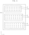
- FIG. 5 illustrates a plan view of a flux coating apparatus of the solder member mounting system in FIG. 1 .
- FIG. 6A illustrates a cross-sectional view of a first flux coater of the flux coating apparatus in FIG. 5 .
- FIG. 6B illustrates a cross-sectional view of a second flux coater of the flux coating apparatus in FIG. 5 .
- FIG. 6C illustrates a cross-sectional view of a third flux coater of the flux coating apparatus in FIG. 5 .
- FIG. 7 illustrates a plan view of a solder member attaching apparatus of the solder member mounting system in FIG. 1 .
- FIG. 8A illustrates a cross-sectional view of a first solder member attacher of the solder member attaching apparatus in FIG. 7 .
- FIG. 8B illustrates a cross-sectional view of a second solder member attacher of the solder member attaching apparatus in FIG. 7 .
- FIG. 8C illustrates a cross-sectional view of a third solder member attacher of the solder member attaching apparatus in FIG. 7 .
- FIG. 9 illustrates a flow chart of a solder member mounting method in accordance with example embodiments.
- FIGS. 10 to 15 illustrate views of stages in the solder member mounting method in FIG. 9 .
- FIGS. 16A to 16C illustrate cross-sectional views of first to third flux coaters of a flux coating apparatus of a solder member mounting system in accordance with example embodiments.
- FIGS. 17A to 17C illustrate cross-sectional views of first to third solder member attachers of a solder member mounting system in accordance with example embodiments.
- FIGS. 18 to 22 illustrate views of a solder member mounting method in accordance with example embodiments.
- FIG. 1 is a block diagram illustrating a solder member mounting system in accordance with example embodiments.
- FIG. 2 is a plan view illustrating a substrate including bonding pads on which solder members are mounted by the solder member mounting system in FIG. 1 .
- FIG. 3A is a cross-sectional view illustrating a substrate including bonding pads with a first pattern interval.
- FIG. 3B is a cross-sectional view illustrating a substrate including bonding pads with a second pattern interval.
- FIG. 3C is a cross-sectional view illustrating a substrate including bonding pads with a third pattern interval.
- FIG. 4 is a block diagram illustrating a controller of the solder member mounting system in FIG. 1 .
- FIG. 1 is a block diagram illustrating a controller of the solder member mounting system in FIG. 1 .
- FIG. 5 is a plan view illustrating a flux coating apparatus of the solder member mounting system in FIG. 1 .
- FIG. 6A is a cross-sectional view illustrating a first flux coater of the flux coating apparatus in FIG. 5 .
- FIG. 6B is a cross-sectional view illustrating a second flux coater of the flux coating apparatus in FIG. 5 .
- FIG. 6C is a cross-sectional view illustrating a third flux coater of the flux coating apparatus in FIG. 5 .
- FIG. 7 is a plan view illustrating a solder member attaching apparatus of the solder member mounting system in FIG. 1 .
- FIG. 8A is a cross-sectional view illustrating a first solder member attacher of the solder member attaching apparatus in FIG. 7 .
- FIG. 8B is a cross-sectional view illustrating a second solder member attacher of the solder member attaching apparatus in FIG. 7 .
- FIG. 8C is a cross-sectional view illustrating a third solder member attacher of the solder member attaching apparatus in FIG. 7 .
- a solder member mounting system 10 may include a substrate transferring stage 100 , a pattern recognition apparatus 200 , a flux coating apparatus 300 , a solder member attaching apparatus 400 , and a controller 500 .
- the solder member mounting system 10 may be configured to mount solder members, e.g., solder balls, on bonding pads 22 on a surface of a substrate 20 at once, e.g., to mount simultaneously a plurality of solder members on the substrate 20 .
- the solder member mounting system 10 may be configured to mount an electronic product on the substrate 20 with the solder balls interposed therebetween.
- the substrate 20 may include a package substrate, e.g., a printed circuit board (PCB), a semiconductor chip, an interposer, etc.
- the bonding pads 22 on which the solder members are attached, may be formed on the surface of the substrate 20 .
- the solder member mounting system 10 may include a main frame 12 configured to support fixedly the substrate transferring stage 100 , the pattern recognition apparatus 200 , the flux coating apparatus 300 , and the solder member attaching apparatus 400 .
- the main frame 12 may include a guide rail along which the substrate transferring stage 100 moves in a horizontal direction and a vertical direction.
- the substrate transferring stage 100 may include a substrate support to support the substrate 20 and a driving unit 110 (see FIG. 13 ) to elevate the substrate support.
- a vacuum suction part for holding the substrate 20 may be provided in the substrate support.
- the driving unit 110 may include a translation driving portion and/or a rotation driving portion for precise position control of the substrate 20 .
- the substrate 20 may be held on the substrate support of the substrate transferring stage 100 , and then, the substrate 20 may be transferred sequentially to the pattern recognition apparatus 200 , the flux coating apparatus 300 , and the solder member attaching apparatus 400 .
- the pattern recognition apparatus 200 may include at least one vision camera for detecting a pattern interval of the bonding pads 22 of the substrate 20 .
- the pattern recognition apparatus 200 may provide a pattern recognition system for recognition of the pattern interval of the bonding pads 22 through the vision camera.
- the pattern interval of the bonding pads 22 of the substrate 20 may be changed due to manufacture tolerance distribution and contraction and expansion of the substrate occurring through thermal processes.
- the bonding pads 22 may have a first pattern interval.
- the bonding pads 22 with the first pattern interval may be spaced apart from each other by a first distance d 1 , e.g., along the X direction and along the Y direction.
- a first allowable error range may be determined such that the first pattern interval of the bonding pads 22 falls within the first allowable error range to prevent soldering failure where the solder member deviates from the bonding pad.
- the bonding pads 22 may have a second pattern interval greater than the first pattern interval.
- the bonding pads 22 with the second pattern interval may be spaced apart from each other by a second distance d 2 greater than the first distance d 1 .
- a second allowable error range may be determined such that the second pattern interval of the bonding pads 22 falls within the second allowable error range to prevent soldering failure of the solder member.
- the bonding pads 22 may have a third pattern interval greater than the second pattern interval.
- the bonding pads 22 with the third pattern interval may be spaced apart from each other by a third distance d 3 greater than the second distance d 2 .
- a third allowable error range may be determined such that the third pattern interval of the bonding pads 22 falls within the third allowable error range to prevent soldering failure of the solder member.
- the first pattern interval when the first pattern interval is 93, the first pattern interval may fall within the first allowable error range of from 85 to 95.
- the second pattern interval when the second pattern interval is 97, the second pattern interval may fall within the second allowable error range of from 95 to 105.
- the third pattern interval is 112, the third pattern interval may fall within the third allowable error range for from 105 to 115.
- the first to third allowable error ranges may be determined by any suitable method in consideration of sizes of the bonding pads, spacing between the bonding pads, size of the solder member, etc.
- the number, size, etc. of the allowable error ranges may be determined in consideration of the spacing between the bonding pads, coefficient of thermal expansion of the substrate, etc.
- the numbers of flux coaters and solder member attachers as described later may be determined based on the number of the determined allowable error ranges.
- the flux coating apparatus 300 may include a plurality of flux coaters, e.g., first to third flux coaters 310 a , 310 b , 310 c .
- the first to third flux coaters 310 a , 310 b , 310 c may have first to third flux pattern intervals corresponding to the first to third allowable error ranges respectively, and may coat, e.g., dot, flux 30 on bonding pads 22 of the substrate 20 before attaching solder balls thereon.
- dots of flux 30 correspond to bottoms of the dotting pins, respectively, in respective flux coaters in FIGS. 6A-6C .
- the first flux coater 310 a may include a first body 320 a and a plurality of first dotting pins 322 a extending in a direction from the first body 320 a .
- the plurality of first dotting pins 322 a may be arranged at equal intervals along the Y direction and the X direction, e.g., in a matrix pattern, and may extend along the Z direction from the first body 320 a .
- the first dotting pins 322 a of the first flux coater 310 a may move to a flux reservoir and dip into flux with end portions of the first dotting pins 322 a , and may dot the flux onto the bonding pads 22 of the substrate 20 .
- the first dotting pins 322 a of the first flux coater 310 a may have a first flux pattern interval which satisfies the first allowable error range.
- the first dotting pins 322 a of the first flux coater 310 a may be spaced apart from each other by a first gap X 1 , e.g., along each of the Y and X directions.
- the second flux coater 310 b may include a second body 320 b and a plurality of second dotting pins 322 b extending in a direction from the second body 320 b .
- the second body 320 b may be adjacent the first body 320 a , e.g., along the Y direction, and may be substantially the same as the first body 320 a , except that the second body 320 b may be longer than the first body 320 a along the X direction and/or the Y direction.
- the second dotting pins 322 b of the second flux coater 310 b may have a second flux pattern interval which satisfies the second allowable error range.
- the second dotting pins 322 b of the second flux coater 310 b may be spaced apart from each other by a second gap X 2 greater than the first gap X 1 , e.g., along the X and/or Y directions. For example, as illustrated in FIG.
- a total number of the second dotting pins 322 b in the second flux coater 310 b may be the same as that of the first dotting pins 322 a in the first flux coater 310 a , and the larger second gap X 2 between the second dotting pins 322 b accounts for the longer length of the second body 320 b.
- the third flux coater 310 c may include a third body 320 c and a plurality of third dotting pins 322 c extending in a direction from the third body 320 c .
- the third body 320 c may be adjacent the second body 320 b , e.g., along the Y direction, and may be substantially the same as the second body 320 b , except that the third body 320 c may be longer than the second body 320 b along the X direction and/or the Y direction.
- the third dotting pins 322 c of the third flux coater 310 c may have a third flux pattern interval which satisfies the third allowable error range.
- the third dotting pins 322 c of the third flux coater 310 c may be spaced apart from each other by a third gap X 3 greater than the second gap X 2 , e.g., along the X and/or Y directions. For example, as illustrated in FIG.
- a total number of the third dotting pins 322 c in the third flux coater 310 c may be the same as that of the first dotting pins 322 a in the first flux coater 310 a , and the larger third gap X 3 between the third dotting pins 322 c accounts for the longer length of the third body 320 c.
- the solder member attaching apparatus 400 may include a plurality of solder member attachers, e.g., first to third solder member attachers 410 a , 410 b , 410 c .
- the first to third attachers 410 a , 410 b , 410 c have first to third solder member pattern intervals corresponding to the first to third allowable error ranges respectively.
- solder balls 40 correspond to bottoms of solder ball holders, respectively, in respective solder member attachers in FIGS. 8A-8C .
- the first solder member attacher 410 a may include a first body 420 a and a first solder ball holder 421 a .
- the first body 420 a may include an inner space connected to an external vacuum supply, e.g., the inner space may extend continuously along the X direction and the Y direction, and the first solder ball holder 421 a may be connected to, e.g., a bottom of, the first body 420 a .
- the first solder ball holder 421 a may include a plurality of first holding-holes 422 a therethrough, e.g., along the z direction, which are connected to the inner space of the first body 420 a .
- a plurality of solder balls 40 may be held selectively in the plurality of first holding-holes 422 a , respectively, by vacuum via the external vacuum supply. For example, a vacuum pressure may be applied to the first holding-holes 422 a such that the first holding-holes 422 a hold the solder balls, and the vacuum pressure may be removed from the first holding-holes 422 a such that the solder balls are dropped to be attached on the bonding pads 22 of the substrate 20 .
- the first holding-holes 422 a of the first solder member attacher 410 a may have a first solder member pattern interval which satisfies the first allowable error range.
- the first holding-holes 422 a of the first solder member attacher 410 a may be spaced apart from each other by a first length Y 1 .
- the second solder member attacher 410 b may include a second body 420 b and a second solder ball holder 421 b with second holding-holes 422 b .
- the second body 420 b may be adjacent the first body 420 a , e.g., along the Y direction, and may be substantially the same as the first body 420 a , except that the second body 420 b may be longer than the first body 420 a along the X direction and/or the Y direction.
- the second holding-holes 422 b of the second solder member attacher 410 b may have a second solder member interval which satisfies the second allowable error range.
- the second holding-holes 422 b of the second solder member attacher 410 b may be spaced apart from each other by a second length Y 2 greater than the first length Y 1 , e.g., along the X and/or Y directions.
- a total number of the second holding-holes 422 b may be the same as that of the first holding-holes 422 a.
- the third solder member attacher 410 c may include a third body 420 c and a third solder ball holder 421 c with third holding-holes 422 c .
- the third body 420 c may be adjacent the second body 420 b , e.g., along the Y direction, and may be substantially the same as the second body 420 b , except that the third body 420 c may be longer than the second body 420 b along the X direction and/or the Y direction.
- the third holding-holes 422 c of the third solder member attacher 410 c may have a third solder member interval which satisfies the third allowable error range.
- the third holding-holes 422 c of the third solder member attacher 410 c may be spaced apart from each other by a third length Y 3 greater than the second length Y 2 e.g., along the X and/or Y directions.
- a total number of the third holding-holes 422 c may be the same as that of the first holding-holes 422 a.
- the controller 500 may include a data receiving portion 510 , a storage portion 520 , and an output portion 530 .
- the data receiving portion 510 may be connected to the pattern recognition apparatus 200 to receive data, e.g., image data, from the pattern recognition apparatus 200 regarding the bonding pads 22 of the substrate 20 , e.g., regarding the pattern and spacing of the bonding pads 22 on the substrate 20 .
- the storage portion 520 may store mapping data of allowable error ranges mapped according to the pattern intervals of the bonding pads 22 .
- the output portion 530 may determine an actual pattern interval of the bonding pads 22 from the image data and an allowable error range mapped to the determined pattern interval.
- the output portion 530 may output a control signal for selecting one of the first to third flux coaters 310 a , 310 b , 310 c , and one of the first to third solder member attachers 410 a , 410 b , 410 c corresponding to the determined allowable error range with respect to the bonding pads 22 on the substrate 20 .
- the substrate transferring stage 100 may transfer the substrate 20 sequentially to the selected flux coater of the flux coating apparatus 300 and the selected solder member attacher of the solder member attaching apparatus 400 according to the control signal from the output portion 530 of the controller 500 .
- the flux coating apparatus 300 may dot the flux 30 on the bonding pads 22 of the substrate 20 using the one selected from the first to third flux coaters 310 a , 310 b , 310 c according to the control signal.
- the solder member attaching apparatus 400 may attach the solder balls 40 on the bonding pads 22 of the substrate 20 using one selected from the first to third solder member attachers 410 a , 410 b , 410 c.
- the solder member mounting system 10 may include the pattern recognition apparatus 200 to recognize the actual pattern interval of the bonding pads 22 of the substrate 20 , which varies according to thermal processes previously performed on the substrate 20 .
- the solder member mounting system 10 may predict different pattern intervals and may include a plurality of the flux coaters 310 a , 310 b , 310 c corresponding to the different pattern intervals and a plurality of the solder member attachers 410 a , 410 b , 410 c corresponding to the different pattern intervals.
- One of the flux coaters 310 a , 310 b , 310 c corresponding to the actual pattern interval may be selected and one of the solder member attachers 410 a , 410 b , 410 c corresponding to the actual pattern interval may be selected. Accordingly, solder balls may be attached at desired positions on the bonding pads 22 of the substrate 20 , thereby preventing solder ball mounting failure where the solder balls deviate from the respective bonding pads.
- FIG. 9 is a flow chart illustrating a solder member mounting method in accordance with example embodiments.
- FIGS. 10 to 15 are views illustrating the solder member mounting method in FIG. 9 .
- the solder member mounting system 10 including the flux coating apparatus 300 having the first to third flux coaters 310 a , 310 b , 310 c with respective pattern intervals and the solder member attaching apparatus 400 having the first to third solder member attachers 410 a , 410 b , 410 c with respective pattern intervals may be prepared (S 10 ). It is noted that while the flux coating apparatus 300 is illustrated to include three flux coaters, and the solder member attaching apparatus 400 is illustrated to include three solder member attachers, example embodiments are not limited thereto and may include more than three of each of the flux coaters and the solder member attachers.
- the substrate 20 may be loaded on the substrate transferring stage 100 of the solder member mounting system 10 , and an actual pattern interval of the bonding pads 22 of the substrate 20 may be detected (S 20 ). That is, the substrate 20 may be loaded onto the substrate support of the substrate transferring stage 100 , and the pattern recognition apparatus 200 may be used to determine the pattern interval of the bonding pads 22 of the substrate 20 .
- a vacuum suction part for holding the substrate 20 may be provided in the substrate support.
- the substrate 20 may include a printed circuit board (PCB), a semiconductor chip, an interposer, etc.
- the bonding pads 22 on which the solder members are to be attached, may be formed on a surface of the substrate 20 .
- a vision camera of the pattern recognition apparatus 200 may move along an extending direction of the substrate 20 to photograph the bonding pads 22 of the substrate 20 , and transmit the photographed image data to the controller 500 .
- the pattern recognition apparatus 200 may extend along an entire short side of the substrate 20 , and may move along a longitudinal direction of the substrate 20 (along arrow in FIG. 10 ) to photograph the entire surface of the substrate 20 that includes the pads 22 and faces the pattern recognition apparatus 200 .
- one of the plurality of the flux coaters 310 a , 310 b , 310 c corresponding to the detected pattern interval may be selected and one of the plurality of the solder member attachers 410 a , 410 b . 410 c corresponding to the detected pattern interval may be selected (S 30 ).
- the substrate 20 with the pads 22 is transferred to the selected flux coater, and flux may be dotted on the bonding pads 22 of the substrate 20 .
- the substrate 20 with the pads 22 is transferred to the selected solder member attacher, and solder balls may be attached on the bonding pads 22 of the substrate 20 using the selected solder member attacher (S 40 ). Then, a solder reflow process may be performed on the substrate 20 to form a solder bump (S 50 ).
- the bonding pads 22 of the substrate 20 may have a pattern interval due to thermal history.
- the controller 500 may determine a plurality of allowable error ranges corresponding to different pattern intervals which are predicted by thermal expansion and thermal contraction of the substrate 20 .
- first to third allowable error ranges may be determined. In case that a standard pattern interval is 100, the first allowable error range may be from 85 to 95, the second allowable error range may be from 95 to 105, and the third allowable error range may be from 105 to 115.
- the bonding pads 22 of the substrate 20 may have a third pattern interval which falls within the third allowable error range.
- flux may be coated on the bonding pads 22 of the substrate 20 using the third flux coater 310 c having the third flux pattern interval corresponding to the third allowable error range.
- the substrate 20 may be transferred to the third flux coater 310 c of the flux coating apparatus 300 (along the arrow in FIG. 11 ).
- the third body 320 c of the third flux coater 310 c may be lowered toward the substrate 20 (along the arrow in FIG. 12 ), and the flux 30 may be dotted on the bonding pads 22 of the substrate 20 by the third dotting pins 322 c of the third flux coater 310 c .
- the third gap X 3 between the third dotting pins 322 c corresponds to the third distance d 3 between the pads 22 , so the third dotting pins 322 c and the pads 22 are aligned.
- the substrate 20 may be transferred to the third solder member attacher 410 c of the solder member attaching apparatus 400 , so the solder balls 40 may be attached on the bonding pads 22 of the substrate 20 using the third solder member attacher 410 c having a third solder member pattern interval corresponding to the third allowable error range.
- the third holding-holes 422 c of the third solder member attacher 410 c may hold and place the solder balls 40 on the bonding pads 22 of the substrate 20 in a vacuum suction manner.
- the third length Y 3 between the third holding-holes 422 c corresponds to the third distance d 3 between the pads 22 , so the third holding-holes 422 c and the pads 22 are aligned.
- the flux 30 and the solder ball 40 may be stacked sequentially on the bonding pad 22 of the substrate 20 . Then, the solder reflow process may be performed on the substrate 20 to form the solder bump (S 50 ).
- the substrate 20 may be transferred to a heating chamber of a solder reflow apparatus, and then, the solder ball may be heated to form the solder bump on the bonding pad 22 of the substrate 20 .
- the flux 30 may be selectively heated by the solder reflow apparatus and the solder ball 40 may be molten to form the solder bump.
- an electronic product may be mounted on the substrate 20 with the solder balls 40 interposed therebetween.
- the substrate 20 and the electronic product may be connected mechanically and electrically to each other.
- FIGS. 16A to 16C are cross-sectional views illustrating first to third flux coaters of a flux coating apparatus of a solder member mounting system in accordance with example embodiments.
- FIGS. 17A to 17C are cross-sectional views illustrating first to third solder member attachers of a solder member mounting system in accordance with example embodiments.
- the solder member mounting system may be substantially the same as or similar to the solder member mounting system described with reference to FIG. 1 , except for configurations of the flux coater and the solder member attacher.
- same reference numerals will be used to refer to the same or like elements and any further repetitive explanation concerning the above elements will be omitted.
- a flux coating apparatus may include first to third flux coaters 310 a ′, 310 b ′, 310 c ′.
- the first to third flux coaters 310 a ′, 310 b ′, 310 c ′ may have first to third flux pattern intervals corresponding to first to third allowable error ranges respectively.
- the first flux coater 310 a ′ may include a frame 340 with a first flux mask 330 a having first through-holes 332 a for coating flux. After the first flux mask 330 a is positioned on the substrate 20 , the flux may be coated on a whole upper surface of the first flux mask 330 a using a screen-printing method. Then, the first flux mask 330 a may be removed from the substrate 20 , so a flux pattern having the first flux pattern interval may remain on the substrate 20 in accordance with the first through-holes 332 a .
- the first through-holes 332 a of the first flux coater 310 a ′ may have the first flux pattern interval which satisfies the first allowable error range.
- the first through-holes 332 a of the first flux coater 310 a ′ may be spaced apart from each other by the first gap X 1 .
- the second flux coater 310 b ′ may include a second flux mask 330 b having second through-holes 332 b for coating flux.
- the second through-holes 332 b of the second flux coater 310 b ′ may have the second flux pattern interval which satisfies the second allowable error range.
- the second through-holes 332 b of the second flux coater 310 b ′ may be spaced apart from each other by the second gap X 2 greater than the first gap X 1 .
- the third flux coater 310 c ′ may include a third flux mask 330 c having third through-holes 332 c for coating flux.
- the third through-holes 332 c of the third flux coater 310 c ′ may have the third flux pattern interval which satisfies the third allowable error range.
- the third through-holes 332 c of the third flux coater 310 c ′ may be spaced apart from each other by the third gap X 3 greater than the second gap X 2 .
- a solder member attaching apparatus may include first to third solder member attachers 410 a ′, 410 b ′, 410 c ′.
- the first to third solder member attachers 410 a ′, 410 b ′, 410 c ′ may have first to third solder member pattern intervals corresponding to the first to third allowable error ranges.
- the first solder member attacher 410 a ′ may include a frame 440 with a first ball mask 430 having first holes 432 a for passing solder balls therethrough. After the first ball mask 430 a is positioned on the substrate 20 , the solder balls may be moved into the first holes 432 a of the first ball mask 430 a using a brush. Then, the first ball mask 430 a may be removed from the substrate 20 to attach a solder ball pattern having the first solder ball pattern interval on the substrate 20 . The first holes 432 a of the first solder member attacher' 410 a may have the first solder member pattern interval which satisfies the first allowable error range. The first holes 432 a of the first solder member attacher 410 a ′ may be spaced apart from each other by a first length Y 1 .
- the second solder member attacher 410 b ′ may include a second ball mask 430 b having second holes 432 b for passing solder balls therethrough.
- the second holes 432 b of the second solder member attacher 410 b ′ may have the second solder member pattern interval which satisfies the second allowable error range.
- the second holes 432 b of the second solder member attacher 410 b ′ may be spaced apart from each other by a second length Y 2 greater than the first length Y 1 .
- the third solder member attacher 410 c ′ may include a third ball mask 430 c having third holes 432 c for passing solder balls therethrough.
- the third holes 432 c of the third solder member attacher 410 c ′ may have the third solder member pattern interval which satisfies the third allowable error range.
- the third holes 432 c of the third solder member attacher 410 c ′ may be spaced apart from each other by a third length Y 3 greater than the second length Y 2 .
- solder member mounting system including the flux coating apparatus in FIGS. 16A to 16C and the solder member attaching apparatus in FIGS. 17A to 17C will be explained.
- FIGS. 18 to 22 are views illustrating a solder member mounting method in accordance with example embodiments.
- the substrate 20 may be loaded on the substrate transferring stage 100 of the solder member mounting system 10 . Then, an actual pattern interval of the bonding pads 22 may be detected.
- a vision camera of the pattern recognition apparatus 200 may move along an extending direction of the substrate 20 to photograph the bonding pads 22 of the substrate 20 , and may transmit the photographed image data to the controller 500 .
- the bonding pads 22 of the substrate 20 may have a pattern interval due to thermal history.
- the controller 500 may determine a plurality of allowable error ranges corresponding to different pattern intervals which are predicted by thermal expansion and thermal contraction of the substrate 20 .
- first to third allowable error ranges may be determined.
- the first allowable error range may be from 85 to 95
- the second allowable error range may be from 95 to 105
- the third allowable error range may be from 105 to 115.
- the bonding pads 22 of the substrate 20 may have the first pattern interval which falls within the first allowable error range.
- flux may be coated on the bonding pads 22 of the substrate 20 using the first flux coater 310 a ′ having the first flux pattern interval corresponding to the first allowable error range.
- the substrate 20 may be transferred to the first flux coater 310 a ′ of the flux coating apparatus 300 .
- the first flux mask 330 a may be positioned on the substrate 20 .
- the flux may be coated on a whole upper surface of the first flux mask 330 a using a screen-printing method.
- the first flux mask 330 a may be removed from the substrate 20 to form a flux pattern having the first flux pattern interval on the substrate 20 .
- solder balls 40 may be attached on the bonding pads 22 of the substrate 20 using the first solder member attacher 410 a ′ having a first solder member pattern interval corresponding to the first allowable error range. That is, as illustrated in FIGS. 21 and 22 , the substrate 20 may be transferred to the first solder member attacher 410 a ′ of the solder member attaching apparatus 400 . After the first ball mask 430 a is positioned on the substrate 20 , the solder balls 40 may be moved into first holes 432 a of the first ball mask 430 a using a brush 450 ( FIG. 22 ), and the first ball mask 430 a may be removed from the substrate 20 to attach a solder ball pattern having the first solder ball pattern interval on the substrate 20 .
- vacuum pressure may be applied to a vacuum holder provided in the solder member attaching apparatus 400 to hold the solder balls 40 , followed by removal of the vacuum pressure from the first holes 432 a and spraying air out to move the solder balls 40 into the respective first holes 432 a , or a cyclone may be used to move the solder balls 40 into the respective first holes 432 a . Then, a solder reflow process may be performed on the substrate 20 to mount the solder balls 40 on the bonding pads 22 of the substrate 20 .
- the solder member attaching apparatus 400 may be included in the solder member mounting system 10 , and the flux coating apparatus 300 may be omitted.
- the solder member attaching apparatus 400 may include first to third paste coaters for coating solder paste.
- the first to third paste coaters may have first to third solder paste pattern intervals corresponding to first to third allowable error ranges respectively.
- each of the first to third paste coaters may include a paste mask having openings for coating the solder paste. After the paste mask is positioned on the substrate 20 , the solder paste may be printed on the bonding pads 22 of the substrate 20 through the openings of the paste mask.
- the semiconductor package may include logic devices, e.g., central processing units (CPUs), main processing units (MPUs), or application processors (APs), or the like, and volatile memory devices, e.g., dynamic random access memory (DRAM) devices, static random access memory (SRAM) devices, or non-volatile memory devices, e.g., flash memory devices, phase change random access memory (PRAM) devices, magnetoresistive random access memory (MRAM) devices, resistive random access memory (ReRAM) devices, or the like.
- logic devices e.g., central processing units (CPUs), main processing units (MPUs), or application processors (APs), or the like
- volatile memory devices e.g., dynamic random access memory (DRAM) devices, static random access memory (SRAM) devices
- non-volatile memory devices e.g., flash memory devices, phase change random access memory (PRAM) devices, magnetoresistive random access memory (MRAM) devices, resistive random access memory (ReRAM) devices, or the
- the methods, processes, and/or operations described herein may be performed by code or instructions to be executed by a computer, processor, controller, or other signal processing device.
- the computer, processor, controller, or other signal processing device may be those described herein or one in addition to the elements described herein. Because the algorithms that form the basis of the methods (or operations of the computer, processor, controller, or other signal processing device) are described in detail, the code or instructions for implementing the operations of the method embodiments may transform the computer, processor, controller, or other signal processing device into a special-purpose processor for performing the methods described herein.
- calculation units, control units, and other processing features of the disclosed embodiments may be implemented in logic which, for example, may include hardware, software, or both.
- the calculation units, control units, and other processing features may be, for example, any one of a variety of integrated circuits including but not limited to an application-specific integrated circuit, a field-programmable gate array, a combination of logic gates, a system-on-chip, a microprocessor, or another type of processing or control circuit.
- the calculation units, control units, and other processing features may include, for example, a memory or other storage device for storing code or instructions to be executed, for example, by a computer, processor, microprocessor, controller, or other signal processing device.
- the computer, processor, microprocessor, controller, or other signal processing device may be those described herein or one in addition to the elements described herein. Because the algorithms that form the basis of the methods (or operations of the computer, processor, microprocessor, controller, or other signal processing device) are described in detail, the code or instructions for implementing the operations of the method embodiments may transform the computer, processor, controller, or other signal processing device into a special-purpose processor for performing the methods described herein.
- solder balls when solder balls are mounted on bonding pads of a substrate at once, a distance between the solder balls may not be matched with a distance between the bonding pads due to contraction and expansion of the substrate during previous processing stages, e.g., according to thermal history. Therefore, a solder ball mounting failure may be caused where the distances between the solder balls deviate from the distances between respective bonding pads.
- example embodiments provide a solder member mounting method capable of manufacturing a semiconductor package or a semiconductor module having electrical reliability.
- Example embodiments also provide a solder member mounting system for performing the solder member mounting method.
- a plurality of allowable error ranges may be determined such that an actual pattern interval of bonding pads of a substrate falls within one of the allowable error ranges.
- Flux coaters having different pattern intervals and solder member attackers having different pattern intervals are provided, with the different pattern intervals corresponding to the allowable error ranges respectively.
- the actual pattern interval of the bonding pads is detected, and flux and solder members are formed sequentially on the bonding pads of the substrate, using the flux coater and the solder member attacher having the pattern interval corresponding to the detected pattern interval. Accordingly, the solder balls may be attached at desired positions on the bonding pads of the substrate, to thereby prevent solder ball mounting failure where distances between the solder balls deviate from distances between the respective bonding pads.
Landscapes
- Engineering & Computer Science (AREA)
- Microelectronics & Electronic Packaging (AREA)
- Manufacturing & Machinery (AREA)
- Mechanical Engineering (AREA)
- Computer Hardware Design (AREA)
- Power Engineering (AREA)
- Electric Connection Of Electric Components To Printed Circuits (AREA)
- Ceramic Engineering (AREA)
- Physics & Mathematics (AREA)
- Condensed Matter Physics & Semiconductors (AREA)
- General Physics & Mathematics (AREA)
Abstract
Description
Claims (20)
Priority Applications (1)
| Application Number | Priority Date | Filing Date | Title |
|---|---|---|---|
| US17/589,925 US11583948B2 (en) | 2018-10-05 | 2022-02-01 | Solder member mounting system |
Applications Claiming Priority (2)
| Application Number | Priority Date | Filing Date | Title |
|---|---|---|---|
| KR1020180119255A KR102528016B1 (en) | 2018-10-05 | 2018-10-05 | Solder member mounting method and system |
| KR10-2018-0119255 | 2018-10-05 |
Related Child Applications (1)
| Application Number | Title | Priority Date | Filing Date |
|---|---|---|---|
| US17/589,925 Continuation US11583948B2 (en) | 2018-10-05 | 2022-02-01 | Solder member mounting system |
Publications (2)
| Publication Number | Publication Date |
|---|---|
| US20200108459A1 US20200108459A1 (en) | 2020-04-09 |
| US11278979B2 true US11278979B2 (en) | 2022-03-22 |
Family
ID=70052608
Family Applications (2)
| Application Number | Title | Priority Date | Filing Date |
|---|---|---|---|
| US16/381,171 Active 2040-03-02 US11278979B2 (en) | 2018-10-05 | 2019-04-11 | Solder member mounting method and system |
| US17/589,925 Active US11583948B2 (en) | 2018-10-05 | 2022-02-01 | Solder member mounting system |
Family Applications After (1)
| Application Number | Title | Priority Date | Filing Date |
|---|---|---|---|
| US17/589,925 Active US11583948B2 (en) | 2018-10-05 | 2022-02-01 | Solder member mounting system |
Country Status (3)
| Country | Link |
|---|---|
| US (2) | US11278979B2 (en) |
| KR (1) | KR102528016B1 (en) |
| CN (1) | CN111010817B (en) |
Families Citing this family (5)
| Publication number | Priority date | Publication date | Assignee | Title |
|---|---|---|---|---|
| TWI736979B (en) * | 2019-09-12 | 2021-08-21 | 啓碁科技股份有限公司 | Electronic device and mainboard and system in package module thereof |
| KR20210101357A (en) * | 2020-02-07 | 2021-08-19 | 삼성전자주식회사 | Ball disposition system and method for ball disposition on substrate |
| US11824037B2 (en) | 2020-12-31 | 2023-11-21 | International Business Machines Corporation | Assembly of a chip to a substrate |
| KR20230090445A (en) * | 2021-12-14 | 2023-06-22 | 삼성전자주식회사 | Manufacturing method of semiconductor package |
| US12318870B2 (en) | 2022-12-22 | 2025-06-03 | Samsung Electronics Co., Ltd. | Ball attachment apparatus |
Citations (53)
| Publication number | Priority date | Publication date | Assignee | Title |
|---|---|---|---|---|
| US4139138A (en) * | 1977-04-07 | 1979-02-13 | Besselman Jr Charles W | Solder tray |
| US4421266A (en) * | 1981-07-29 | 1983-12-20 | Western Electric Company, Inc. | Handling bodies containing bonding material |
| US5676305A (en) * | 1996-04-18 | 1997-10-14 | Motorola, Inc. | Method to achieve regulated force contact in pin transfer deposition of liquidus substances |
| US5695667A (en) * | 1995-02-07 | 1997-12-09 | Matsushita Electric Industrial Co., Ltd. | Method and apparatus for mounting soldering balls onto electrodes of a substrate or a comparable electronic component |
| US5816481A (en) * | 1997-01-24 | 1998-10-06 | Unisys Corporation | Pin block method of dispensing solder flux onto the I/O pads of an integrated circuit package |
| US5834062A (en) * | 1996-06-27 | 1998-11-10 | Motorola, Inc. | Material transfer apparatus and method of using the same |
| KR19990055886A (en) | 1997-12-29 | 1999-07-15 | 구본준 | VISION Package Ball Mounting Head |
| US6193132B1 (en) * | 1997-11-27 | 2001-02-27 | Kabushiki Kaisha Toshiba | Method for bonding semiconductor chip and device therefor |
| US20010008249A1 (en) * | 1997-01-28 | 2001-07-19 | Eric Lee Hertz | Method and apparatus for release and optional inspection for conductive preforms placement apparatus |
| US6317513B2 (en) * | 1996-12-19 | 2001-11-13 | Cognex Corporation | Method and apparatus for inspecting solder paste using geometric constraints |
| US20020084315A1 (en) * | 1997-05-27 | 2002-07-04 | Mackay John | Ball bumping substrates, particuarly wafers |
| US6460755B1 (en) * | 1996-03-08 | 2002-10-08 | Hitachi, Ltd. | Bump forming method and apparatus therefor |
| US6607117B1 (en) * | 1999-10-15 | 2003-08-19 | Samsung Electronics Co., Ltd. | Solder ball attaching system and method |
| US20030175599A1 (en) * | 2002-03-13 | 2003-09-18 | Apostolos Voutsas | Symmetrical mask system and method for laser irradiation |
| US20040031406A1 (en) * | 2002-08-19 | 2004-02-19 | Matsushita Electric Industrial Co., Ltd. | Method for forming printing inspection data |
| US20040035306A1 (en) * | 1996-05-22 | 2004-02-26 | Hiroaki Onishi | Solder paste printing apparatus and printing method |
| US20050035182A1 (en) * | 2003-08-11 | 2005-02-17 | Niigata Seimitsu Co., Ltd. | Circuit board transferring apparatus and method and solder ball mounting method |
| US20050077340A1 (en) * | 2001-03-06 | 2005-04-14 | Matsushita Electric Industrial Co., Ltd. | Method, apparatus, system, method and device for data creating, and program for mounting electronic component |
| US20050087886A1 (en) * | 2003-10-27 | 2005-04-28 | Leinbach Glen E. | Method and apparatus for improving defective solder joint detection using x-ray inspection of printed assemblies |
| US20050133573A1 (en) * | 2003-12-23 | 2005-06-23 | Arthur Bayot | Solder contact reworking using a flux plate and sequeegee |
| US20050232728A1 (en) * | 2004-03-31 | 2005-10-20 | Rice Michael R | Methods and apparatus for transferring conductive pieces during semiconductor device fabrication |
| KR20060016939A (en) | 2004-08-19 | 2006-02-23 | 삼성전자주식회사 | Heterogeneous solder ball forming device of semiconductor device |
| US7112889B1 (en) * | 1999-11-11 | 2006-09-26 | Fujitsu Limited | Semiconductor device having an alignment mark formed by the same material with a metal post |
| US20070102478A1 (en) * | 2005-11-10 | 2007-05-10 | Speedline Technologies, Inc. | Optimal imaging system and method for a stencil printer |
| US20080048009A1 (en) * | 2004-11-04 | 2008-02-28 | Tadashi Maeda | Paste For Soldering And Soldering Method Using The Same |
| US20080054047A1 (en) * | 2006-08-31 | 2008-03-06 | Houssam Jomaa | Microball placement solutions |
| US20080182398A1 (en) | 2007-01-30 | 2008-07-31 | Carpenter Burton J | Varied Solder Mask Opening Diameters Within a Ball Grid Array Substrate |
| US20080197170A1 (en) * | 2007-02-16 | 2008-08-21 | Prince David P | Single and multi-spectral illumination system and method |
| US7506792B1 (en) * | 2007-05-04 | 2009-03-24 | Manfroy John V | Solder sphere placement apparatus |
| US7507655B2 (en) | 2006-04-11 | 2009-03-24 | Shinko Electric Industries, Co., Ltd. | Method of forming solder connection portions, method of forming wiring substrate and method of producing semiconductor device |
| US20090122306A1 (en) * | 2005-11-15 | 2009-05-14 | Omron Corporation | Solder Material Inspecting Device |
| US20090294516A1 (en) * | 2008-05-30 | 2009-12-03 | Ibiden, Co., Ltd. | Solder ball loading mask, apparatus and associated methodology |
| US20120006364A1 (en) * | 2010-07-06 | 2012-01-12 | Kim Jong-Guw | Flux cleaning apparatus |
| KR20140013594A (en) | 2012-07-25 | 2014-02-05 | 삼성전기주식회사 | Solder ball mounting mask, solder ball mounting apparatus, solder ball mounting system and method for mounting solder ball using the same |
| KR101371332B1 (en) | 2013-01-07 | 2014-03-10 | 주식회사 고려반도체시스템 | Apparatus and method of dotting flux on plural solder balls attached on chip before stacking process |
| US8671561B2 (en) * | 2007-05-24 | 2014-03-18 | Shinko Electric Industries Co., Ltd. | Substrate manufacturing method |
| US8799845B2 (en) * | 2010-02-16 | 2014-08-05 | Deca Technologies Inc. | Adaptive patterning for panelized packaging |
| US20140242753A1 (en) * | 2013-02-27 | 2014-08-28 | Samsung Electronics Co., Ltd. | Flip chip packaging method, and flux head manufacturing method applied to the same |
| US20150231723A1 (en) | 2014-02-17 | 2015-08-20 | Samsung Electronics Co., Ltd. | Solder ball attaching apparatus, flux dotting apparatus, and method of manufacturing semiconductor package |
| US20150287788A1 (en) * | 2011-09-06 | 2015-10-08 | Infineon Technologies Ag | Method for Making a Sensor Device Using a Graphene Layer |
| US20160035696A1 (en) * | 2013-12-05 | 2016-02-04 | Nantong Fujitsu Microelectronics Co., Ltd. | Method for forming package structure |
| US9579741B2 (en) | 2014-07-21 | 2017-02-28 | Samsung Electronics Co., Ltd. | Apparatus for adsorbing solder ball and method of attaching solder ball using the same |
| US20170257951A1 (en) * | 2014-09-09 | 2017-09-07 | Mycronic AB | Method and device for applying solder paste flux |
| US20170261455A1 (en) * | 2014-11-24 | 2017-09-14 | Lg Innotek Co., Ltd. | Gas sensor package |
| US20180005972A1 (en) * | 2016-07-01 | 2018-01-04 | Intel Corporation | Interface structures for packaged circuitry and method of providing same |
| US20180049356A1 (en) * | 2016-08-10 | 2018-02-15 | Omron Corporation | Inspection apparatus and quality control system for surface mounting line |
| US20180277449A1 (en) * | 2017-03-27 | 2018-09-27 | Renesas Electronics Corporation | Manufacturing method of semiconductor device, inspection device of semiconductor device, and semiconductor device |
| US20190267346A1 (en) * | 2018-02-28 | 2019-08-29 | Powertech Technology Inc. | Flux transfer tool and flux transfer method |
| US20190275600A1 (en) * | 2018-03-07 | 2019-09-12 | Powertech Technology Inc. | Flux transfer tool and flux transfer method |
| US20190295976A1 (en) * | 2018-03-20 | 2019-09-26 | Toshiba Memory Corporation | Semiconductor fabrication apparatus and semiconductor fabrication method |
| US20190378815A1 (en) * | 2017-01-27 | 2019-12-12 | Detection Technology Oy | Laser assisted solder bonding of direct conversion compound semiconductor detector |
| US20200120796A1 (en) * | 2017-07-06 | 2020-04-16 | Fujikura Ltd. | Substrate module and method for producing substrate module |
| US20200331062A1 (en) * | 2014-06-09 | 2020-10-22 | Hybrid Manufacturing Technologies Limited | Material processing methods and related apparatus |
Family Cites Families (12)
| Publication number | Priority date | Publication date | Assignee | Title |
|---|---|---|---|---|
| US5749614A (en) * | 1995-12-04 | 1998-05-12 | Motorola, Inc. | Vacuum pickup tool for placing balls in a customized pattern |
| JPH1174407A (en) * | 1997-08-29 | 1999-03-16 | Mitsubishi Electric Corp | Semiconductor device |
| KR20050012506A (en) * | 2003-07-25 | 2005-02-02 | 삼성전자주식회사 | Flux dotting apparatus |
| DE102004025279B4 (en) * | 2004-05-19 | 2011-04-28 | Infineon Technologies Ag | System for equipping substrates with ball contacts and method for equipping substrates with ball contacts |
| TWI458410B (en) * | 2006-11-22 | 2014-10-21 | 洛科企業有限公司 | Improvement of ball planting device and method |
| US20090108053A1 (en) * | 2007-10-26 | 2009-04-30 | Huddleston Wyatt A | Solder Ball Placement Vacuum Tool |
| JP5930021B2 (en) * | 2012-03-08 | 2016-06-08 | 富士通株式会社 | Electronic component inspection apparatus and method |
| JP2014011231A (en) * | 2012-06-28 | 2014-01-20 | Hitachi Ltd | Solder ball printing mounting device |
| KR102034820B1 (en) * | 2012-11-30 | 2019-11-08 | 삼성전자주식회사 | Apparatus for mounting semiconductor chips on a circuit board and method of mounting semiconductor chips on a circuit using the same |
| KR101416650B1 (en) * | 2014-02-25 | 2014-07-09 | 주식회사 고려반도체시스템 | Solderball attach apparatus and solderball supplying device used therein |
| US9721855B2 (en) * | 2014-12-12 | 2017-08-01 | International Business Machines Corporation | Alignment of three dimensional integrated circuit components |
| JP2018056228A (en) * | 2016-09-27 | 2018-04-05 | ルネサスエレクトロニクス株式会社 | Semiconductor device, system in package, and in-vehicle system in package |
-
2018
- 2018-10-05 KR KR1020180119255A patent/KR102528016B1/en active Active
-
2019
- 2019-04-11 US US16/381,171 patent/US11278979B2/en active Active
- 2019-06-17 CN CN201910520730.7A patent/CN111010817B/en active Active
-
2022
- 2022-02-01 US US17/589,925 patent/US11583948B2/en active Active
Patent Citations (54)
| Publication number | Priority date | Publication date | Assignee | Title |
|---|---|---|---|---|
| US4139138A (en) * | 1977-04-07 | 1979-02-13 | Besselman Jr Charles W | Solder tray |
| US4421266A (en) * | 1981-07-29 | 1983-12-20 | Western Electric Company, Inc. | Handling bodies containing bonding material |
| US5695667A (en) * | 1995-02-07 | 1997-12-09 | Matsushita Electric Industrial Co., Ltd. | Method and apparatus for mounting soldering balls onto electrodes of a substrate or a comparable electronic component |
| US6460755B1 (en) * | 1996-03-08 | 2002-10-08 | Hitachi, Ltd. | Bump forming method and apparatus therefor |
| US5676305A (en) * | 1996-04-18 | 1997-10-14 | Motorola, Inc. | Method to achieve regulated force contact in pin transfer deposition of liquidus substances |
| US20040035306A1 (en) * | 1996-05-22 | 2004-02-26 | Hiroaki Onishi | Solder paste printing apparatus and printing method |
| US5834062A (en) * | 1996-06-27 | 1998-11-10 | Motorola, Inc. | Material transfer apparatus and method of using the same |
| US6317513B2 (en) * | 1996-12-19 | 2001-11-13 | Cognex Corporation | Method and apparatus for inspecting solder paste using geometric constraints |
| US5816481A (en) * | 1997-01-24 | 1998-10-06 | Unisys Corporation | Pin block method of dispensing solder flux onto the I/O pads of an integrated circuit package |
| US20010008249A1 (en) * | 1997-01-28 | 2001-07-19 | Eric Lee Hertz | Method and apparatus for release and optional inspection for conductive preforms placement apparatus |
| US20020084315A1 (en) * | 1997-05-27 | 2002-07-04 | Mackay John | Ball bumping substrates, particuarly wafers |
| US6193132B1 (en) * | 1997-11-27 | 2001-02-27 | Kabushiki Kaisha Toshiba | Method for bonding semiconductor chip and device therefor |
| KR19990055886A (en) | 1997-12-29 | 1999-07-15 | 구본준 | VISION Package Ball Mounting Head |
| US6607117B1 (en) * | 1999-10-15 | 2003-08-19 | Samsung Electronics Co., Ltd. | Solder ball attaching system and method |
| US7112889B1 (en) * | 1999-11-11 | 2006-09-26 | Fujitsu Limited | Semiconductor device having an alignment mark formed by the same material with a metal post |
| US20050077340A1 (en) * | 2001-03-06 | 2005-04-14 | Matsushita Electric Industrial Co., Ltd. | Method, apparatus, system, method and device for data creating, and program for mounting electronic component |
| US20030175599A1 (en) * | 2002-03-13 | 2003-09-18 | Apostolos Voutsas | Symmetrical mask system and method for laser irradiation |
| US20040031406A1 (en) * | 2002-08-19 | 2004-02-19 | Matsushita Electric Industrial Co., Ltd. | Method for forming printing inspection data |
| US20050035182A1 (en) * | 2003-08-11 | 2005-02-17 | Niigata Seimitsu Co., Ltd. | Circuit board transferring apparatus and method and solder ball mounting method |
| US20050087886A1 (en) * | 2003-10-27 | 2005-04-28 | Leinbach Glen E. | Method and apparatus for improving defective solder joint detection using x-ray inspection of printed assemblies |
| US20050133573A1 (en) * | 2003-12-23 | 2005-06-23 | Arthur Bayot | Solder contact reworking using a flux plate and sequeegee |
| US20050232728A1 (en) * | 2004-03-31 | 2005-10-20 | Rice Michael R | Methods and apparatus for transferring conductive pieces during semiconductor device fabrication |
| KR20060016939A (en) | 2004-08-19 | 2006-02-23 | 삼성전자주식회사 | Heterogeneous solder ball forming device of semiconductor device |
| US20080048009A1 (en) * | 2004-11-04 | 2008-02-28 | Tadashi Maeda | Paste For Soldering And Soldering Method Using The Same |
| US20070102478A1 (en) * | 2005-11-10 | 2007-05-10 | Speedline Technologies, Inc. | Optimal imaging system and method for a stencil printer |
| US20090122306A1 (en) * | 2005-11-15 | 2009-05-14 | Omron Corporation | Solder Material Inspecting Device |
| US7507655B2 (en) | 2006-04-11 | 2009-03-24 | Shinko Electric Industries, Co., Ltd. | Method of forming solder connection portions, method of forming wiring substrate and method of producing semiconductor device |
| US20080054047A1 (en) * | 2006-08-31 | 2008-03-06 | Houssam Jomaa | Microball placement solutions |
| US20080182398A1 (en) | 2007-01-30 | 2008-07-31 | Carpenter Burton J | Varied Solder Mask Opening Diameters Within a Ball Grid Array Substrate |
| US20080197170A1 (en) * | 2007-02-16 | 2008-08-21 | Prince David P | Single and multi-spectral illumination system and method |
| US7506792B1 (en) * | 2007-05-04 | 2009-03-24 | Manfroy John V | Solder sphere placement apparatus |
| US8671561B2 (en) * | 2007-05-24 | 2014-03-18 | Shinko Electric Industries Co., Ltd. | Substrate manufacturing method |
| US20090294516A1 (en) * | 2008-05-30 | 2009-12-03 | Ibiden, Co., Ltd. | Solder ball loading mask, apparatus and associated methodology |
| US8799845B2 (en) * | 2010-02-16 | 2014-08-05 | Deca Technologies Inc. | Adaptive patterning for panelized packaging |
| US20120006364A1 (en) * | 2010-07-06 | 2012-01-12 | Kim Jong-Guw | Flux cleaning apparatus |
| US20150287788A1 (en) * | 2011-09-06 | 2015-10-08 | Infineon Technologies Ag | Method for Making a Sensor Device Using a Graphene Layer |
| KR20140013594A (en) | 2012-07-25 | 2014-02-05 | 삼성전기주식회사 | Solder ball mounting mask, solder ball mounting apparatus, solder ball mounting system and method for mounting solder ball using the same |
| KR101371332B1 (en) | 2013-01-07 | 2014-03-10 | 주식회사 고려반도체시스템 | Apparatus and method of dotting flux on plural solder balls attached on chip before stacking process |
| US20140242753A1 (en) * | 2013-02-27 | 2014-08-28 | Samsung Electronics Co., Ltd. | Flip chip packaging method, and flux head manufacturing method applied to the same |
| US20160035696A1 (en) * | 2013-12-05 | 2016-02-04 | Nantong Fujitsu Microelectronics Co., Ltd. | Method for forming package structure |
| US20150231723A1 (en) | 2014-02-17 | 2015-08-20 | Samsung Electronics Co., Ltd. | Solder ball attaching apparatus, flux dotting apparatus, and method of manufacturing semiconductor package |
| KR20150097841A (en) | 2014-02-17 | 2015-08-27 | 삼성전자주식회사 | Apparatus for attaching solder balls and apparatus for dotting flux |
| US20200331062A1 (en) * | 2014-06-09 | 2020-10-22 | Hybrid Manufacturing Technologies Limited | Material processing methods and related apparatus |
| US9579741B2 (en) | 2014-07-21 | 2017-02-28 | Samsung Electronics Co., Ltd. | Apparatus for adsorbing solder ball and method of attaching solder ball using the same |
| US20170257951A1 (en) * | 2014-09-09 | 2017-09-07 | Mycronic AB | Method and device for applying solder paste flux |
| US20170261455A1 (en) * | 2014-11-24 | 2017-09-14 | Lg Innotek Co., Ltd. | Gas sensor package |
| US20180005972A1 (en) * | 2016-07-01 | 2018-01-04 | Intel Corporation | Interface structures for packaged circuitry and method of providing same |
| US20180049356A1 (en) * | 2016-08-10 | 2018-02-15 | Omron Corporation | Inspection apparatus and quality control system for surface mounting line |
| US20190378815A1 (en) * | 2017-01-27 | 2019-12-12 | Detection Technology Oy | Laser assisted solder bonding of direct conversion compound semiconductor detector |
| US20180277449A1 (en) * | 2017-03-27 | 2018-09-27 | Renesas Electronics Corporation | Manufacturing method of semiconductor device, inspection device of semiconductor device, and semiconductor device |
| US20200120796A1 (en) * | 2017-07-06 | 2020-04-16 | Fujikura Ltd. | Substrate module and method for producing substrate module |
| US20190267346A1 (en) * | 2018-02-28 | 2019-08-29 | Powertech Technology Inc. | Flux transfer tool and flux transfer method |
| US20190275600A1 (en) * | 2018-03-07 | 2019-09-12 | Powertech Technology Inc. | Flux transfer tool and flux transfer method |
| US20190295976A1 (en) * | 2018-03-20 | 2019-09-26 | Toshiba Memory Corporation | Semiconductor fabrication apparatus and semiconductor fabrication method |
Also Published As
| Publication number | Publication date |
|---|---|
| CN111010817B (en) | 2024-07-05 |
| US20200108459A1 (en) | 2020-04-09 |
| US20220152718A1 (en) | 2022-05-19 |
| CN111010817A (en) | 2020-04-14 |
| KR20200039383A (en) | 2020-04-16 |
| KR102528016B1 (en) | 2023-05-02 |
| US11583948B2 (en) | 2023-02-21 |
Similar Documents
| Publication | Publication Date | Title |
|---|---|---|
| US11583948B2 (en) | Solder member mounting system | |
| JP6510838B2 (en) | Bonding apparatus and bonding method | |
| EP2617053B1 (en) | Apparatus and method for generating patterns on workpieces | |
| US20070069752A1 (en) | Electronic device test apparatus | |
| US6976616B2 (en) | Circuit board transferring apparatus and method and solder ball mounting method | |
| US20060290369A1 (en) | Electronic part test device | |
| US10699923B2 (en) | Transfer system for flipping and multiple checking of electronic devices | |
| CN105826217A (en) | Bonding device and bonding method | |
| TWI661749B (en) | An assembly and method for handling components | |
| JP6835808B2 (en) | Use of mountable marker parts for stepwise mounting of parts on the carrier | |
| JP7465197B2 (en) | Element mounting equipment | |
| CN103426787A (en) | Method of inspecting printed circuit boards of semiconductor packages | |
| JP2009054759A (en) | Anomaly detection method and apparatus | |
| WO2007148422A1 (en) | Calibration method employed in electronic component test system | |
| KR20000076544A (en) | Machine for mounting electronic components | |
| TW202343155A (en) | Printing system and method for producing electric component mounting substrate having functional pattern | |
| JP2013143462A (en) | Thin film forming device and thin film forming method | |
| WO2019016978A1 (en) | Imaging device, bump inspection device, and imaging method | |
| JP5317857B2 (en) | Backup pin placement method, placement device, electronic component processing method, and electronic component placement device | |
| JP6804905B2 (en) | Board work equipment | |
| JP4881216B2 (en) | On-board device and method for controlling the same | |
| CN116636321A (en) | Component mounting apparatus and component mounting method | |
| KR20080102061A (en) | Alignment vision method and apparatus | |
| JPH0278300A (en) | Automatic mounting method of electronic component | |
| JPWO2020188745A1 (en) | Arithmetic logic unit and input device |
Legal Events
| Date | Code | Title | Description |
|---|---|---|---|
| AS | Assignment |
Owner name: SAMSUNG ELECTRONICS CO., LTD., KOREA, REPUBLIC OF Free format text: ASSIGNMENT OF ASSIGNORS INTEREST;ASSIGNOR:LEE, SOO-HWAN;REEL/FRAME:048856/0747 Effective date: 20190402 |
|
| FEPP | Fee payment procedure |
Free format text: ENTITY STATUS SET TO UNDISCOUNTED (ORIGINAL EVENT CODE: BIG.); ENTITY STATUS OF PATENT OWNER: LARGE ENTITY |
|
| STPP | Information on status: patent application and granting procedure in general |
Free format text: NON FINAL ACTION MAILED |
|
| STPP | Information on status: patent application and granting procedure in general |
Free format text: RESPONSE TO NON-FINAL OFFICE ACTION ENTERED AND FORWARDED TO EXAMINER |
|
| STPP | Information on status: patent application and granting procedure in general |
Free format text: FINAL REJECTION MAILED |
|
| STPP | Information on status: patent application and granting procedure in general |
Free format text: RESPONSE AFTER FINAL ACTION FORWARDED TO EXAMINER |
|
| STPP | Information on status: patent application and granting procedure in general |
Free format text: ADVISORY ACTION MAILED |
|
| STPP | Information on status: patent application and granting procedure in general |
Free format text: DOCKETED NEW CASE - READY FOR EXAMINATION |
|
| STPP | Information on status: patent application and granting procedure in general |
Free format text: NOTICE OF ALLOWANCE MAILED -- APPLICATION RECEIVED IN OFFICE OF PUBLICATIONS |
|
| STCF | Information on status: patent grant |
Free format text: PATENTED CASE |
|
| MAFP | Maintenance fee payment |
Free format text: PAYMENT OF MAINTENANCE FEE, 4TH YEAR, LARGE ENTITY (ORIGINAL EVENT CODE: M1551); ENTITY STATUS OF PATENT OWNER: LARGE ENTITY Year of fee payment: 4 |