US11271282B2 - Display device for mobile electronic device - Google Patents
Display device for mobile electronic device Download PDFInfo
- Publication number
- US11271282B2 US11271282B2 US15/655,358 US201715655358A US11271282B2 US 11271282 B2 US11271282 B2 US 11271282B2 US 201715655358 A US201715655358 A US 201715655358A US 11271282 B2 US11271282 B2 US 11271282B2
- Authority
- US
- United States
- Prior art keywords
- disposed
- display device
- window
- antenna
- antenna sheet
- Prior art date
- Legal status (The legal status is an assumption and is not a legal conclusion. Google has not performed a legal analysis and makes no representation as to the accuracy of the status listed.)
- Active, expires
Links
Images


Classifications
-
- H—ELECTRICITY
- H10—SEMICONDUCTOR DEVICES; ELECTRIC SOLID-STATE DEVICES NOT OTHERWISE PROVIDED FOR
- H10K—ORGANIC ELECTRIC SOLID-STATE DEVICES
- H10K59/00—Integrated devices, or assemblies of multiple devices, comprising at least one organic light-emitting element covered by group H10K50/00
-
- H—ELECTRICITY
- H01—ELECTRIC ELEMENTS
- H01Q—ANTENNAS, i.e. RADIO AERIALS
- H01Q1/00—Details of, or arrangements associated with, antennas
- H01Q1/12—Supports; Mounting means
- H01Q1/22—Supports; Mounting means by structural association with other equipment or articles
- H01Q1/2258—Supports; Mounting means by structural association with other equipment or articles used with computer equipment
- H01Q1/2266—Supports; Mounting means by structural association with other equipment or articles used with computer equipment disposed inside the computer
-
- G—PHYSICS
- G06—COMPUTING; CALCULATING OR COUNTING
- G06F—ELECTRIC DIGITAL DATA PROCESSING
- G06F1/00—Details not covered by groups G06F3/00 - G06F13/00 and G06F21/00
- G06F1/16—Constructional details or arrangements
- G06F1/1613—Constructional details or arrangements for portable computers
- G06F1/1633—Constructional details or arrangements of portable computers not specific to the type of enclosures covered by groups G06F1/1615 - G06F1/1626
- G06F1/1637—Details related to the display arrangement, including those related to the mounting of the display in the housing
- G06F1/1652—Details related to the display arrangement, including those related to the mounting of the display in the housing the display being flexible, e.g. mimicking a sheet of paper, or rollable
-
- G—PHYSICS
- G06—COMPUTING; CALCULATING OR COUNTING
- G06F—ELECTRIC DIGITAL DATA PROCESSING
- G06F1/00—Details not covered by groups G06F3/00 - G06F13/00 and G06F21/00
- G06F1/16—Constructional details or arrangements
- G06F1/1613—Constructional details or arrangements for portable computers
- G06F1/1633—Constructional details or arrangements of portable computers not specific to the type of enclosures covered by groups G06F1/1615 - G06F1/1626
- G06F1/1684—Constructional details or arrangements related to integrated I/O peripherals not covered by groups G06F1/1635 - G06F1/1675
- G06F1/1698—Constructional details or arrangements related to integrated I/O peripherals not covered by groups G06F1/1635 - G06F1/1675 the I/O peripheral being a sending/receiving arrangement to establish a cordless communication link, e.g. radio or infrared link, integrated cellular phone
-
- H01L27/3225—
-
- H—ELECTRICITY
- H01—ELECTRIC ELEMENTS
- H01Q—ANTENNAS, i.e. RADIO AERIALS
- H01Q1/00—Details of, or arrangements associated with, antennas
- H01Q1/12—Supports; Mounting means
- H01Q1/22—Supports; Mounting means by structural association with other equipment or articles
- H01Q1/2283—Supports; Mounting means by structural association with other equipment or articles mounted in or on the surface of a semiconductor substrate as a chip-type antenna or integrated with other components into an IC package
-
- H—ELECTRICITY
- H01—ELECTRIC ELEMENTS
- H01Q—ANTENNAS, i.e. RADIO AERIALS
- H01Q1/00—Details of, or arrangements associated with, antennas
- H01Q1/36—Structural form of radiating elements, e.g. cone, spiral, umbrella; Particular materials used therewith
- H01Q1/38—Structural form of radiating elements, e.g. cone, spiral, umbrella; Particular materials used therewith formed by a conductive layer on an insulating support
-
- H—ELECTRICITY
- H01—ELECTRIC ELEMENTS
- H01Q—ANTENNAS, i.e. RADIO AERIALS
- H01Q1/00—Details of, or arrangements associated with, antennas
- H01Q1/44—Details of, or arrangements associated with, antennas using equipment having another main function to serve additionally as an antenna, e.g. means for giving an antenna an aesthetic aspect
-
- H—ELECTRICITY
- H01—ELECTRIC ELEMENTS
- H01Q—ANTENNAS, i.e. RADIO AERIALS
- H01Q9/00—Electrically-short antennas having dimensions not more than twice the operating wavelength and consisting of conductive active radiating elements
- H01Q9/04—Resonant antennas
- H01Q9/0407—Substantially flat resonant element parallel to ground plane, e.g. patch antenna
-
- H—ELECTRICITY
- H10—SEMICONDUCTOR DEVICES; ELECTRIC SOLID-STATE DEVICES NOT OTHERWISE PROVIDED FOR
- H10K—ORGANIC ELECTRIC SOLID-STATE DEVICES
- H10K50/00—Organic light-emitting devices
- H10K50/80—Constructional details
- H10K50/86—Arrangements for improving contrast, e.g. preventing reflection of ambient light
-
- H—ELECTRICITY
- H10—SEMICONDUCTOR DEVICES; ELECTRIC SOLID-STATE DEVICES NOT OTHERWISE PROVIDED FOR
- H10K—ORGANIC ELECTRIC SOLID-STATE DEVICES
- H10K59/00—Integrated devices, or assemblies of multiple devices, comprising at least one organic light-emitting element covered by group H10K50/00
- H10K59/10—OLED displays
- H10K59/12—Active-matrix OLED [AMOLED] displays
- H10K59/126—Shielding, e.g. light-blocking means over the TFTs
-
- H—ELECTRICITY
- H10—SEMICONDUCTOR DEVICES; ELECTRIC SOLID-STATE DEVICES NOT OTHERWISE PROVIDED FOR
- H10K—ORGANIC ELECTRIC SOLID-STATE DEVICES
- H10K59/00—Integrated devices, or assemblies of multiple devices, comprising at least one organic light-emitting element covered by group H10K50/00
- H10K59/30—Devices specially adapted for multicolour light emission
- H10K59/38—Devices specially adapted for multicolour light emission comprising colour filters or colour changing media [CCM]
-
- H—ELECTRICITY
- H10—SEMICONDUCTOR DEVICES; ELECTRIC SOLID-STATE DEVICES NOT OTHERWISE PROVIDED FOR
- H10K—ORGANIC ELECTRIC SOLID-STATE DEVICES
- H10K59/00—Integrated devices, or assemblies of multiple devices, comprising at least one organic light-emitting element covered by group H10K50/00
- H10K59/40—OLEDs integrated with touch screens
-
- H—ELECTRICITY
- H10—SEMICONDUCTOR DEVICES; ELECTRIC SOLID-STATE DEVICES NOT OTHERWISE PROVIDED FOR
- H10K—ORGANIC ELECTRIC SOLID-STATE DEVICES
- H10K77/00—Constructional details of devices covered by this subclass and not covered by groups H10K10/80, H10K30/80, H10K50/80 or H10K59/80
- H10K77/10—Substrates, e.g. flexible substrates
- H10K77/111—Flexible substrates
-
- G—PHYSICS
- G06—COMPUTING; CALCULATING OR COUNTING
- G06F—ELECTRIC DIGITAL DATA PROCESSING
- G06F1/00—Details not covered by groups G06F3/00 - G06F13/00 and G06F21/00
- G06F1/16—Constructional details or arrangements
- G06F1/1613—Constructional details or arrangements for portable computers
- G06F1/1633—Constructional details or arrangements of portable computers not specific to the type of enclosures covered by groups G06F1/1615 - G06F1/1626
- G06F1/1637—Details related to the display arrangement, including those related to the mounting of the display in the housing
- G06F1/1643—Details related to the display arrangement, including those related to the mounting of the display in the housing the display being associated to a digitizer, e.g. laptops that can be used as penpads
-
- G—PHYSICS
- G06—COMPUTING; CALCULATING OR COUNTING
- G06F—ELECTRIC DIGITAL DATA PROCESSING
- G06F3/00—Input arrangements for transferring data to be processed into a form capable of being handled by the computer; Output arrangements for transferring data from processing unit to output unit, e.g. interface arrangements
- G06F3/01—Input arrangements or combined input and output arrangements for interaction between user and computer
- G06F3/03—Arrangements for converting the position or the displacement of a member into a coded form
- G06F3/041—Digitisers, e.g. for touch screens or touch pads, characterised by the transducing means
- G06F3/0412—Digitisers structurally integrated in a display
-
- H01L27/3244—
-
- H—ELECTRICITY
- H10—SEMICONDUCTOR DEVICES; ELECTRIC SOLID-STATE DEVICES NOT OTHERWISE PROVIDED FOR
- H10K—ORGANIC ELECTRIC SOLID-STATE DEVICES
- H10K2102/00—Constructional details relating to the organic devices covered by this subclass
- H10K2102/301—Details of OLEDs
- H10K2102/311—Flexible OLED
-
- H—ELECTRICITY
- H10—SEMICONDUCTOR DEVICES; ELECTRIC SOLID-STATE DEVICES NOT OTHERWISE PROVIDED FOR
- H10K—ORGANIC ELECTRIC SOLID-STATE DEVICES
- H10K59/00—Integrated devices, or assemblies of multiple devices, comprising at least one organic light-emitting element covered by group H10K50/00
- H10K59/10—OLED displays
- H10K59/12—Active-matrix OLED [AMOLED] displays
-
- Y—GENERAL TAGGING OF NEW TECHNOLOGICAL DEVELOPMENTS; GENERAL TAGGING OF CROSS-SECTIONAL TECHNOLOGIES SPANNING OVER SEVERAL SECTIONS OF THE IPC; TECHNICAL SUBJECTS COVERED BY FORMER USPC CROSS-REFERENCE ART COLLECTIONS [XRACs] AND DIGESTS
- Y02—TECHNOLOGIES OR APPLICATIONS FOR MITIGATION OR ADAPTATION AGAINST CLIMATE CHANGE
- Y02E—REDUCTION OF GREENHOUSE GAS [GHG] EMISSIONS, RELATED TO ENERGY GENERATION, TRANSMISSION OR DISTRIBUTION
- Y02E10/00—Energy generation through renewable energy sources
- Y02E10/50—Photovoltaic [PV] energy
- Y02E10/549—Organic PV cells
Definitions
- the present disclosure relates to a display device, and more specifically, to a display device capable of being applied to a mobile electronic device.
- a mobile electronic device such as a smart phone, a smart watch, a tablet PC, and the like, uses various wireless communication technologies to send and receive data.
- wireless communication technologies include a wireless local area network (w-LAN), such as Wi-Fi technology, Bluetooth, and near field communication (NFC), as well as cellular mobile communication network technologies such as GSM, CDMA, and LTE.
- w-LAN wireless local area network
- Wi-Fi technology
- Bluetooth Bluetooth
- NFC near field communication
- GSM Global System for Mobile communications
- CDMA Code Division Multiple Access
- LTE long term evolution
- the mobile electronic device includes one or more antenna for facilitating the wireless communication.
- the antenna as a component of the communication device, is generally mounted outside a display device and inside a case of the mobile electronic device.
- a display device includes a display panel having a display area, in which an image is displayed, and a non-display area, in which no image is displayed.
- a window overlaps the display panel.
- An antenna sheet is disposed between the display panel and the window.
- the antenna sheet includes a first antenna portion having a mesh shape, and a second antenna portion integrally connected to the first antenna portion and having a frame shape. The first antenna portion corresponds to the display area and the second antenna portion corresponds to the non-display area.
- a mobile electronic device includes a display panel having a display area in which a plurality of pixels are disposed, and a peripheral region surrounding the display area.
- a window has a light-blocking frame and a transparent interior.
- the light-blocking frame substantially aligns with the peripheral region of the display panel and the transparent interior substantially aligns with the display area of the display panel.
- An antenna sheet is disposed between the display panel and the window.
- the antenna sheet includes a solid portion substantially aligning with the light-blocking frame of the window and the peripheral region of the display panel.
- the antenna sheet further includes a mesh portion substantially aligning with the transparent interior of the window and the display area of the display panel.
- FIG. 1 is an exploded perspective view illustrating a display device according to an exemplary embodiment of the present inventive concept
- FIG. 2 is a cross-sectional view illustrating a bonding shape of a display device shown in FIG. 1 ;
- FIG. 3 is an enlarged cross-sectional view illustrating an organic light emitting panel of a display panel of a display device shown in FIG. 1 , according to an exemplary embodiment of the present inventive concept;
- FIG. 4 is a partially enlarged view illustrating an antenna sheet in a display device shown in FIG. 1 ;
- FIG. 5A to FIG. 5D are cross-sectional views illustrating a manufacturing process of an antenna sheet in a display device shown in FIG. 1 ;
- FIG. 6 is a partial cross-sectional view illustrating a display device according to an exemplary embodiment of the present inventive concept
- FIG. 7 is a partial cross-sectional view illustrating a display device according to an exemplary embodiment of the present inventive concept
- FIG. 8 is a partial cross-sectional view illustrating a display device according to an exemplary embodiment of the present inventive concept
- FIG. 9 is a partial cross-sectional view illustrating a display device according to an exemplary embodiment of the present inventive concept.
- FIG. 10 is a partial cross-sectional view illustrating a display device according to an exemplary embodiment of the present inventive concept
- FIG. 11 is a partial cross-sectional view illustrating a display device according to an exemplary embodiment of the present inventive concept.
- FIG. 12A and FIG. 12B are partial cross-sectional views illustrating a display device according to an exemplary embodiment of the present inventive concept.
- FIG. 1 is an exploded perspective view of a display device according to an exemplary embodiment of the present inventive concept
- FIG. 2 is a cross-sectional view showing a bonding shape of a display device shown in FIG. 1 .
- the display device 100 include a display panel 10 , a window 20 overlapping the display panel 10 , and an antenna sheet 30 disposed between the display panel 10 and the window 20 .
- a polarization film 40 may be disposed between the display panel 10 and the antenna sheet 30 , and a touch panel 50 may be disposed between the antenna sheet 30 and the window 20 .
- a cover panel may be disposed at the back of the display panel 10 .
- the display panel 10 may an organic light emitting panel, a liquid crystal panel, or an electrophoretic display panel, however, the display panel may alternatively be of a different type than those listed.
- the display panel 10 includes a display area DA for displaying an image and a non-display area NDA enclosing the display area DA.
- the non-display area NDA may have a quadrangular frame shape, and when the display area DA is circular, the non-display area NDA may have a circular ring shape.
- the display panel 10 may be a flexible display panel including a flexible substrate.
- FIG. 1 shows a flexible display panel 10 bent along one direction as an example.
- the window 20 , the touch panel 50 , the antenna sheet 30 , and the polarization film 40 are also bent with the same curvature as the flexible display panel 10 .
- FIG. 3 is an enlarged cross-sectional view of an exemplary organic light emitting panel of a display panel of a display device shown in FIG. 1 .
- a structure of the display panel that is described below is an exemplary embodiment of the present inventive concept, and the display panel is not limited to the below-described structure.
- the organic light emitting panel includes a substrate 110 , and a display unit 120 and a thin film encapsulation 130 formed on the substrate 110 .
- the substrate 110 may be a flexible substrate such as a plastic film.
- the flexible substrate 110 may be a multi-layered structure in which two polyimide films are deposited via a silicon nitride layer or a silicon oxide layer interposed therebetween.
- a lower protection film 111 may be disposed under the flexible substrate 110 , and an upper protection film may be disposed on the thin film encapsulation 130 .
- the display unit 120 includes a plurality of pixels and is disposed within the display area DA of the substrate 110 .
- the display unit 120 may include an organic light emitting element 140 , an insulating layer 150 , and a thin film transistor 160 connected to the organic light emitting element 140 .
- the display unit 120 may further include a scan wire, a data wire, a capacitor, and other thin film transistors.
- the thin film transistor 160 includes a semiconductor layer 161 , a gate electrode 162 , a source electrode 163 , and a drain electrode 164 .
- the semiconductor layer 161 includes a channel region, which is not doped with an impurity, and a source region and a drain region, which are disposed at opposite sides of the channel region and are doped with an impurity.
- the gate insulating layer 162 is formed on the semiconductor layer 161 .
- the source electrode 163 and the drain electrode 164 are disposed on the gate electrode 162 and are respectively connected to the source region and the drain region of the semiconductor layer 161 through contact holes.
- the insulating layer 150 includes a first sub-insulating layer 151 , a second sub-insulating layer 152 , and a third sub-insulating layer 153 .
- the first sub-insulating layer 151 is disposed between the substrate 110 and the semiconductor layer 161 , flattens/planarizes the surface of the substrate 110 , and prevents moisture from permeating from the substrate 110 toward the semiconductor layer 161 .
- the second sub-insulating layer 152 covers the semiconductor layer 161 and prevents a short circuit between the semiconductor layer 161 and the gate electrode 162 .
- the third sub-insulating layer 153 covers the gate electrode 162 and prevents a short circuit between the gate electrode 162 and the source electrode 163 and prevents a short circuit between the gate electrode 162 and the drain electrode 164 .
- the organic light emitting element 140 includes a first electrode 141 connected to the drain electrode 164 of the thin film transistor 160 , an organic emission layer 142 disposed on the first electrode 141 , and a second electrode 143 disposed on the organic emission layer 142 .
- One of the first electrode 141 and the second electrode 143 is an anode as a hole injection electrode, and the other is a cathode as an electron injection electrode.
- the first electrode 141 is disposed one by one for each pixel, and the second electrode 143 is disposed throughout the entire display area DA.
- Light emitted from the organic emission layer 142 may be transmitted through the first electrode 141 and the substrate 110 , or may be transmitted through the second electrode 143 and the thin film encapsulation 130 .
- the substrate 110 is disposed closer to the window 20 than is the thin film encapsulation 130 (referring to FIG. 1 )
- the thin film encapsulation 130 is disposed closer to the window 20 than is the substrate 110 (referring to FIG. 1 ).
- element number 154 indicates a planarization layer covering the source electrode 163 and the drain electrode 164
- element number 155 indicates a pixel definition layer defining a formation region of the organic emission layer 142 .
- the thin film encapsulation 130 covers the display unit 120 to isolate the display unit 120 from external air.
- the thin film encapsulation 130 may include multiple layers of an inorganic layer and an organic layer.
- the thin film encapsulation 130 includes a first inorganic layer 131 disposed on the second electrode 143 , an organic layer 132 disposed on the first inorganic layer 131 , and a second inorganic layer 133 disposed on the organic layer 132 .
- Other organic layers and other inorganic layers may be further disposed on the second inorganic layer 133 .
- the insulating layer 150 may be entirely disposed on the display area DA and the non-display area NDA.
- a plurality of blocking layers 170 may be disposed on the insulating layer 150 in the non-display area NDA.
- the plurality of blocking layers 170 are disposed with a predetermined distance therebetween along a surface direction (a horizontal direction based on FIG. 3 ) of the substrate 110 .
- the first inorganic layer 131 and the second inorganic layer 133 may be disposed throughout the entire non-display area NDA while covering the plurality of blocking layers 170 , and the edge of the organic layer 132 may be disposed to be closer to the display area DA than the plurality of blocking layers 170 .
- the plurality of blocking layers 170 prevents the organic layer 132 from overflowing when forming the thin film encapsulation 130 .
- At least one circuit element 180 may be disposed between the display unit 120 and the blocking layer 170 .
- the circuit element 180 performs transmission or conversion of an electric signal to drive the organic light emitting element 140 .
- the polarization film 40 is disposed on the display panel 10 .
- the polarization film 40 may include multiple layers of a linear polarization layer and a 1 ⁇ 4 wavelength layer (quarter-wave plate).
- the polarization film 40 may suppress external light reflection.
- incident external light is linearly-polarized by the linear polarization layer and is circularly-polarized, in one direction, while passing through the 1 ⁇ 4 wavelength layer (quarter-wave plate).
- the rotation direction is reversed while the circular polarized light is reflected by the metal layers of the display unit 120 , and the circular polarized light is converted to linearly polarized light while passing through the 1 ⁇ 4 wavelength layer (quarter-wave plate).
- a vibration direction of the linearly polarized light is perpendicular to a transmissive axis of the linear polarization layer such that the linearly polarized light does not pass through the linear polarization layer.
- the antenna sheet 30 to receive and transmit a wireless signal is disposed on the polarization film 40 .
- a size of the antenna sheet 30 may be larger than the size of the display area DA, and may be equal to or smaller than the size of the display panel 10 .
- a first adhesive layer 61 may be disposed between the antenna sheet 30 and the polarization film 40 .
- FIG. 4 is a partially enlarged view of an antenna sheet in a display device shown in FIG. 1 .
- the antenna sheet 30 includes a base material film 31 and a metal layer 32 disposed on the base material film 31 .
- the metal layer 32 includes a first antenna portion 33 of a mesh shape corresponding to the display area DA of the display panel 10 , and a second antenna portion 34 enclosing the first antenna portion 33 and corresponding to the non-display area NDA of the display panel 10 .
- the first antenna portion 33 includes a plurality of first metal lines 331 extending along a first direction DR 1 , and a plurality of second metal lines 332 extending along a second direction DR 2 crossing the first direction DR 1 .
- the plurality of first metal lines 331 and the plurality of second metal lines 332 are integrally connected to each other at side surfaces thereof.
- the antenna sheet 30 may have a pair of long sides 301 and a pair of short sides 302 , and the first direction DR 1 and the second direction DR 2 may be diagonal directions of the antenna sheet 30 crossing both of the long side 301 and the short side 302 .
- the first antenna portion 33 includes a plurality of openings OP.
- the plurality of openings OP are respectively disposed between two adjacent first metal lines 331 and between two adjacent second metal lines 332 . In the entire first antenna portion 33 , the plurality of opening OP may have the same size and may be uniformly disposed.
- the plurality of first metal lines 331 and the plurality of second metal lines 332 may have the same width.
- the plurality of first metal lines 331 may be aligned with a predetermined distance between each other, and the plurality of second metal lines 332 may be aligned with a predetermined distance between each other.
- a distance between two adjacent first metal lines 331 may be the same as a distance between two adjacent second metal lines 332 .
- the plurality of first metal lines 331 and the plurality of second metal lines 332 may have a width of about 2 ⁇ m to 3 ⁇ m, respectively.
- the size of the plurality of openings OP is larger than the size of one of pixels provided in the display unit 120 , and a plurality of pixels are disposed to correspond to one opening OP.
- the first antenna portion 33 transmits light emitted in the display area DA of the display panel 10 through the plurality of openings OP toward the window 20 .
- the first antenna portion. 33 is not observed by the naked eye such that the first antenna unit 33 may be substantially transparent and may have a light transmittance of about 80% to 90%.
- the second antenna portion 34 is integrally connected with the first antenna portion 33 .
- an end part of the plurality of first metal lines 331 and an end part of the plurality of second metal lines 332 are integrally connected with an inner side surface of the second antenna portion 34 .
- the second antenna portion 34 has the frame shape corresponding to the non-display area NDA of the display panel 10 and does not have openings thereby having a higher density than the first antenna portion 33 .
- the second antenna portion 34 reinforces the performance of the first antenna portion 33 , thereby increasing the performance of the antenna sheet 30 .
- the antenna sheet 30 may include a resin layer 35 disposed between the base material film 31 and the metal layer 32 .
- the resin layer 35 may include a recess portion with the same shape as the metal layer 32 , and the metal layer 32 may be disposed at the recess portion.
- the antenna sheet 30 may be manufactured by a process that is described in detail below.
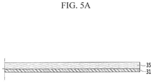
- FIG. 5A to FIG. 5D are cross-sectional views showing a manufacturing process of an antenna sheet in a display device shown in FIG. 1 .
- the manufacturing process shown in FIG. 5 A to FIG. 5D represents an exemplary embodiment of the present inventive concept, and the antenna sheet may be manufactured in other ways.
- a resin layer 35 is formed on a base material film 31 .
- the resin layer 35 may include an ultraviolet ray curing resin and may be formed by a general coating method.
- an imprint mold presses the resin layer 35 to form a recess portion 36 at an upper surface of the resin layer 35 .
- the recess portion 36 has the same shape as a metal layer that is previously designed.
- a metal paste 37 is printed on the recess portion 36 of the resin layer 35 .
- the metal paste 37 includes metal particles of silver, copper, and/or aluminum, and organic materials.
- the resin layer 35 and the metal paste 37 are exposed ultraviolet rays during a thermal treatment.
- the resin layer 35 is cured hard by the ultraviolet rays and the organic materials included in the metal paste are removed by the thermal treatment, thereby completing a metal layer 32 .
- a thickness of the metal layer 32 may be smaller than a depth of the recess portion 36 .
- the resin layer 35 includes the recess portion 36 and the metal layer 32 is disposed at the recess portion 36 , spreading of the metal paste 37 may be prevented in the manufacturing process of the antenna sheet 30 . Accordingly, in the first antenna portion 33 , a plurality of first metal lines 331 and a plurality of second metal lines 332 may maintain an intended minute line width.
- the opening OP of the first antenna portion 33 is filled with the resin layer 35 .
- the antenna sheet 30 may further include an access member 38 fixed to the second antenna portion 34 .
- the access member 38 is electrically connected to a controller.
- a touch panel 50 is disposed on the antenna sheet 30 .
- a second adhesive layer 62 may be disposed between the antenna sheet 30 and the touch panel 50 .
- the touch panel 50 as an input device of the display device 100 , includes a touch sensor capable of sensing touch input inputting information generated by contacting a screen by a finger or a pen of a user.
- the touch sensor may be operated by various methods, for example, the touch sensor may be of a capacitive type for sensing a position where a capacitance change is generated depending on the point of contact.
- the touch panel 50 may have various structures.
- the window 20 is disposed on the touch panel 50 .
- the window 20 is disposed at a highest part of the display device 100 to protect the touch panel 50 and the display panel 1 from an impact or external interference.
- a third adhesive layer 63 may be disposed between the touch panel 50 and the window 20 .
- the window 20 may include a transparent substrate 21 and a light blocking film 22 disposed directly under the transparent substrate 21 and corresponding to the non-display area NDA of the display panel 10 .
- a part that does not overlap the light blocking film 22 is a light transmission region, and a part overlapping the light blocking film 22 is a light blocking region.
- the light blocking film 22 prevents the non-display area NDA of the display panel 10 from being seen by the user.
- the display device 100 of the above-described approach includes the antenna sheet 30 overlapping the display panel 10 . Accordingly, the electronic device including the display device 100 , for example, the mobile electronic device, may do without a separate antenna that is disposed outside the display device 100 such that the entire structure may be simplified and the entire thickness may be minimized.
- FIG. 6 is a partial cross-sectional view of a display device according to an exemplary embodiment of the present inventive concept.
- the antenna sheet 30 is disposed directly under the window 20 , and the second antenna portion 34 of the antenna sheet 30 functions as the light blocking film.
- the size of the antenna sheet 30 may be the same as the size of the window 20 .
- the window 20 is made of the transparent substrate, and the antenna sheet 30 is in contact with a lower surface of the transparent substrate.
- the part overlapping the first antenna portion 33 becomes the light transmission region
- the part overlapping the second antenna portion 34 becomes the light blocking region.
- the second antenna portion 34 does not transmit the light, thereby preventing the non-display area NDA of the display panel 10 from being recognized at the side of the user.
- the touch panel 50 may be disposed on the polarization film 40 , and a fourth adhesive layer 64 may be disposed between the polarization film 40 and the touch panel 50 .
- the antenna sheet 30 and the window 20 may be disposed on the touch panel 50 , and a fifth adhesive layer 65 may be disposed between the touch panel 50 and the antenna sheet 30 .
- a base material film 31 of the antenna sheet 30 may be in contact with the lower surface of the window 20 , and the metal layer 32 may be in contact with the fifth adhesive layer 65 .
- the display device 200 may omit the light blocking film described above because of the integral structure of the window 20 and the antenna sheet 30 , and one of the adhesive layers may be omitted, as compared with the approach described above.
- the display device 200 here may be made with a configuration that is the same as or similar to that of one of the display device of the above-described exemplary embodiment, except for the omission of the light blocking film and the position of the antenna sheet 30 .
- FIG. 7 is a partial cross-sectional view of a display device according to an exemplary embodiment of the present inventive concept.
- the antenna sheet 30 is disposed between the display panel 10 and the touch panel 50 , and the polarization film 40 is disposed on the touch panel 50 .
- the antenna sheet 30 may be disposed on the display panel 10
- a sixth adhesive layer 66 may be disposed between the display panel 10 and the antenna sheet 30
- the touch panel 50 may be disposed on the antenna sheet 30
- a seventh adhesive layer 67 may be disposed between the antenna sheet 30 and the touch panel 50
- the polarization film 40 may be disposed on the touch panel 50
- the window 20 may be disposed on the polarization film 40
- An eighth adhesive layer 68 may be disposed between the polarization film 40 and the window 20 .
- the window 20 may include the transparent substrate 21 as well as the light blocking film 22 corresponding to the non-display area NDA of the display panel 10 .
- the light blocking film 22 prevents the non-display area NDA of the display panel 10 from being seen by the user.
- the display device 300 may be made with a configuration that is the same as or similar to that of one of the above-described approach except for the polarization film 40 being disposed on the touch panel 50 .
- FIG. 8 is a partial cross-sectional view of a display device according to an exemplary embodiment of the present inventive concept.
- the display panel 10 includes a color filter layer 410 , and the touch panel 50 is disposed between the antenna sheet 30 and the window 20 .
- the color filter layer 410 includes a red filter, a blue filter, and a green filter arranged in parallel with a predetermined distance therebetween. Each of the red filter, the blue filter, and the green filter may correspond to one organic light emitting element 140 (referring to FIG. 3 ) disposed at the display unit 120 .
- the color filter layer 410 may include a black color layer disposed between the red filter, the blue filter, and the green filter.
- Each of the red filter, the blue filter, and the green filter absorbs visible light that is of a color other than its own specific color, thereby reducing external reflection.
- the black color layer absorbs all visible light components of the external light incident to the display device. Accordingly, the color filter layer may replace the polarization film described above.
- the display device 400 may be made with a configuration that is the same as or similar to that of one of the above-described approach except for the polarization film that is replaced by the color filter layer 410 of the display panel 10 .
- FIG. 9 is a partial cross-sectional view of a display device according to an exemplary embodiment of the present inventive concept.
- the display panel 10 includes a touch sensing unit 510 , and the polarization film 40 is disposed between the antenna sheet 30 and the window 20 .
- the touch sensing unit 510 uses a film that may allow for the omission of the substrate.
- the touch sensing unit 510 may include a plurality of touch sensing electrodes disposed on an upper protection film covering the thin film encapsulation 130 (referring to FIG. 3 ).
- the display device 500 may be made with a configuration that is the same as or similar to that of one of the above-described embodiment except for the touch panel that is replaced with the touch sensing unit 510 of the display panel 10 .
- FIG. 10 is a partial cross-sectional view of a display device according to an exemplary embodiment of the present inventive concept.
- the display panel 10 includes the color filter layer 410 , and the touch panel 50 is disposed between the display panel 10 and the antenna sheet 30 .
- the structure of the color filter layer 410 may be the same as an approach described above and any details omitted may be understood to be similar to or the same as corresponding details that have already been described.
- the display device 600 may be made with a configuration that is the same as or similar to that of one of the above-described configurations except for the polarization film that is replaced with the color filter layer 410 of the display panel 10 .
- FIG. 11 is a partial cross-sectional view of a display device according to an exemplary embodiment of the present inventive concept.
- the display panel 10 includes the touch sensing unit 510 , and the polarization film 40 is disposed between the touch sensing unit 510 and the antenna sheet 30 .
- the structure of the touch sensing unit 510 may be the same as that of one of the approaches described above and any details omitted may be understood to be similar to or the same as corresponding details that have already been described.
- the display device 700 may be made with a configuration that is the same as or similar to that of one of the above-described approaches except for the touch panel that is replaced with the touch sensing unit 510 .
- FIG. 12A and FIG. 12B are partial cross-sectional views of a display device according to an exemplary embodiment of the present inventive concept.
- the display panel 10 includes the color filter layer 410 and the touch sensing unit 510 .
- the structure of the color filter layer 410 may be the same as that of the one of the approaches described above and the structure of the touch sensing unit 510 is the same as one of the approaches described above and any details omitted may be understood to be similar to or the same as corresponding details that have already been described.
- the color filter layer 410 is disposed between the display unit 120 and the touch sensing unit 510 .
- the color filter layer 410 and the touch sensing unit 510 may share the substrate.
- the plurality of color filters and the black color layer may be disposed at one surface of the substrate, and the plurality of touch sensing electrodes may be disposed at the other surface of the substrate.
- the touch sensing unit 510 is disposed between the display unit 120 and the color filter layer 410 .
- the touch sensing unit 510 may use the upper protection film covering the thin film encapsulation 130 (referring to FIG. 3 ) as the substrate.
- the antenna sheet 30 is disposed between the display panel 10 and the window 20 .
- the polarization film 40 and the touch panel 50 are disposed between the display panel 10 and the antenna sheet 30 , however they may alternatively be disposed between the antenna sheet 30 and the window 20 .
- the display panel 10 includes either the color filter layer 410 or the touch sensing unit 510 .
- the color filter layer 410 replaces the polarization film, and the touch sensing unit 510 replaces the touch panel.
- the display devices 400 , 500 , 600 , 700 , and 800 may reduce the total thickness.
Landscapes
- Engineering & Computer Science (AREA)
- Computer Hardware Design (AREA)
- Theoretical Computer Science (AREA)
- General Engineering & Computer Science (AREA)
- Physics & Mathematics (AREA)
- Human Computer Interaction (AREA)
- General Physics & Mathematics (AREA)
- Microelectronics & Electronic Packaging (AREA)
- Optics & Photonics (AREA)
- Devices For Indicating Variable Information By Combining Individual Elements (AREA)
- Details Of Aerials (AREA)
Abstract
Description
Claims (19)
Priority Applications (1)
| Application Number | Priority Date | Filing Date | Title |
|---|---|---|---|
| US17/689,354 US20220200128A1 (en) | 2016-07-28 | 2022-03-08 | Display device for mobile electronic device |
Applications Claiming Priority (2)
| Application Number | Priority Date | Filing Date | Title |
|---|---|---|---|
| KR1020160096329A KR102666192B1 (en) | 2016-07-28 | Display device | |
| KR10-2016-0096329 | 2016-07-28 |
Related Child Applications (1)
| Application Number | Title | Priority Date | Filing Date |
|---|---|---|---|
| US17/689,354 Continuation US20220200128A1 (en) | 2016-07-28 | 2022-03-08 | Display device for mobile electronic device |
Publications (2)
| Publication Number | Publication Date |
|---|---|
| US20180034130A1 US20180034130A1 (en) | 2018-02-01 |
| US11271282B2 true US11271282B2 (en) | 2022-03-08 |
Family
ID=61010170
Family Applications (2)
| Application Number | Title | Priority Date | Filing Date |
|---|---|---|---|
| US15/655,358 Active 2038-08-29 US11271282B2 (en) | 2016-07-28 | 2017-07-20 | Display device for mobile electronic device |
| US17/689,354 Pending US20220200128A1 (en) | 2016-07-28 | 2022-03-08 | Display device for mobile electronic device |
Family Applications After (1)
| Application Number | Title | Priority Date | Filing Date |
|---|---|---|---|
| US17/689,354 Pending US20220200128A1 (en) | 2016-07-28 | 2022-03-08 | Display device for mobile electronic device |
Country Status (2)
| Country | Link |
|---|---|
| US (2) | US11271282B2 (en) |
| CN (1) | CN107665914B (en) |
Cited By (1)
| Publication number | Priority date | Publication date | Assignee | Title |
|---|---|---|---|---|
| US20220102851A1 (en) * | 2020-09-28 | 2022-03-31 | Boe Technology Group Co., Ltd. | Antenna, Preparation Method Thereof and Electronic Device |
Families Citing this family (30)
| Publication number | Priority date | Publication date | Assignee | Title |
|---|---|---|---|---|
| JP2018060404A (en) * | 2016-10-06 | 2018-04-12 | 株式会社ジャパンディスプレイ | Display device and correction method for touch operation |
| KR20180078860A (en) * | 2016-12-30 | 2018-07-10 | 엘지디스플레이 주식회사 | Antenna Integrated Polarizer and Flexible Display Device Using the Same |
| CN111164829A (en) * | 2017-09-25 | 2020-05-15 | 天传知识产权有限公司 | System, apparatus and method for improving antenna performance in an electronic device |
| CN107887527A (en) * | 2017-11-06 | 2018-04-06 | 京东方科技集团股份有限公司 | OLED display panel and preparation method, encapsulation part failure determination methods, display device |
| KR102405146B1 (en) * | 2018-02-08 | 2022-06-08 | 삼성디스플레이 주식회사 | Organic light-emitting display device and method of manufacturing the same |
| TWI659253B (en) * | 2018-02-13 | 2019-05-11 | 友達光電股份有限公司 | Display device |
| CN111048549B (en) * | 2018-10-11 | 2022-08-16 | 上海和辉光电股份有限公司 | Display panel, display device and preparation method of display panel |
| KR102147439B1 (en) * | 2018-10-17 | 2020-08-24 | 동우 화인켐 주식회사 | Antenna-deco film stack structure and display device including the same |
| US20200192542A1 (en) * | 2018-12-12 | 2020-06-18 | Novatek Microelectronics Corp. | Display device with integrated antenna and method thereof |
| JP7271162B2 (en) * | 2018-12-19 | 2023-05-11 | 株式会社ジャパンディスプレイ | Electronics |
| KR20200082674A (en) * | 2018-12-31 | 2020-07-08 | 엘지디스플레이 주식회사 | Display apparatus with integrated antenna |
| WO2020147079A1 (en) * | 2019-01-17 | 2020-07-23 | 京东方科技集团股份有限公司 | Display apparatus and manufacturing method therefor |
| JP6902064B2 (en) * | 2019-04-17 | 2021-07-14 | Nissha株式会社 | Display device |
| EP3984095A4 (en) * | 2019-06-12 | 2023-06-21 | 3M Innovative Properties Company | Transparent antenna stack and assembly |
| CN112243051B (en) * | 2019-07-17 | 2021-10-22 | 北京小米移动软件有限公司 | Mobile terminal, antenna control method, and storage medium |
| CN114208139B (en) * | 2019-08-21 | 2024-04-12 | 华为技术有限公司 | Display stack for electronic device |
| CN112635980A (en) * | 2019-09-24 | 2021-04-09 | 北京小米移动软件有限公司 | Light-transmitting film antenna and mobile communication terminal having the same |
| KR20210042202A (en) * | 2019-10-08 | 2021-04-19 | 삼성디스플레이 주식회사 | Display apparatus |
| KR20210049326A (en) * | 2019-10-25 | 2021-05-06 | 엘지디스플레이 주식회사 | Flexible display device |
| KR20210052749A (en) * | 2019-10-31 | 2021-05-11 | 삼성디스플레이 주식회사 | Display apparatus and electronic apparatus having the same |
| CN112928438B (en) * | 2019-11-20 | 2023-10-20 | 华为技术有限公司 | Cover plate and electronic equipment |
| CN210984952U (en) * | 2019-12-06 | 2020-07-10 | 昇印光电(昆山)股份有限公司 | Transparent antenna |
| CN113067916B (en) * | 2020-01-02 | 2024-01-30 | 昆山国显光电有限公司 | Display module and display terminal |
| CN111463245B (en) * | 2020-04-10 | 2024-03-08 | 京东方科技集团股份有限公司 | Display substrate, manufacturing method thereof and display device |
| KR20210127000A (en) * | 2020-04-13 | 2021-10-21 | 동우 화인켐 주식회사 | Antenna integrated display panel |
| KR20210130332A (en) | 2020-04-21 | 2021-11-01 | 삼성디스플레이 주식회사 | Electronic device |
| CN111430443A (en) | 2020-04-29 | 2020-07-17 | 武汉华星光电半导体显示技术有限公司 | Organic light emitting display and manufacturing method thereof |
| KR20220049681A (en) | 2020-10-14 | 2022-04-22 | 삼성디스플레이 주식회사 | Electronic device |
| CN113612872A (en) * | 2021-07-27 | 2021-11-05 | 青岛海信移动通信技术股份有限公司 | Terminal equipment and millimeter wave radar module |
| CN116897470A (en) * | 2022-01-29 | 2023-10-17 | 京东方科技集团股份有限公司 | Antenna, display substrate and display device |
Citations (18)
| Publication number | Priority date | Publication date | Assignee | Title |
|---|---|---|---|---|
| US20090051620A1 (en) * | 2005-04-01 | 2009-02-26 | Tatsuo Ishibashi | Transparent Antenna for Display, Translucent Member for Display With an Antenna and Housing Component With an Antenna |
| US20100021695A1 (en) * | 2006-12-27 | 2010-01-28 | Susumu Naoyuki | Engraved plate and substrate with conductor layer pattern using the same |
| KR20110010199U (en) | 2010-04-22 | 2011-10-28 | 삼성전자주식회사 | Antenna apparatus for performing multiple functions and portable terminal having the same |
| US20120287017A1 (en) * | 2011-05-10 | 2012-11-15 | Harris Corporation, Corporation Of The State Of Delaware | Electronic device including electrically conductive mesh layer patch antenna and related methods |
| US20120287002A1 (en) * | 2011-05-11 | 2012-11-15 | Harris Corporation, Corporation Of The State Of Delaware | Electronic device including a patch antenna and visual display layer and related methods |
| US20120287018A1 (en) * | 2011-05-11 | 2012-11-15 | Harris Corporation, Corporation Of The State Of Delaware | Electronic device including a patch antenna and photovoltaic layer and related methods |
| US20140106684A1 (en) * | 2012-10-15 | 2014-04-17 | Qualcomm Mems Technologies, Inc. | Transparent antennas on a display device |
| US20140139379A1 (en) * | 2012-11-16 | 2014-05-22 | Sony Mobile Communications Ab | Transparent antennas for wireless terminals |
| JP5682464B2 (en) | 2011-06-13 | 2015-03-11 | 大日本印刷株式会社 | Transparent antenna and image display device |
| KR20160050467A (en) | 2014-10-29 | 2016-05-11 | 삼성전자주식회사 | Antenna device for electronic device with the same |
| US20160190678A1 (en) * | 2014-12-29 | 2016-06-30 | Samsung Electronics Co., Ltd. | Antenna Device and Electronic Device Including the Same |
| US20160344089A1 (en) * | 2015-05-22 | 2016-11-24 | Samsung Electronics Co., Ltd. | Display module and method of manufacturing the same |
| EP3098699A1 (en) * | 2015-05-08 | 2016-11-30 | Intel Corporation | Display integrated antenna |
| US20160351634A1 (en) * | 2015-05-27 | 2016-12-01 | Samsung Electronics Co., Ltd. | Display device |
| US20160351855A1 (en) * | 2012-09-28 | 2016-12-01 | Apple Inc. | Borderless Display With Light-Bending Structures |
| US20180046283A1 (en) * | 2015-05-19 | 2018-02-15 | Fujifilm Corporation | Antenna, method of manufacturing antenna, and touch sensor |
| US20190004662A1 (en) * | 2017-07-03 | 2019-01-03 | Essential Products, Inc. | Touch-sensitive electronic device chasses |
| US10474282B2 (en) * | 2016-03-31 | 2019-11-12 | Samsung Electronics Co., Ltd. | Electronic device including antenna device |
Family Cites Families (20)
| Publication number | Priority date | Publication date | Assignee | Title |
|---|---|---|---|---|
| US3356833A (en) * | 1963-08-02 | 1967-12-05 | Pittsburgh Plate Glass Co | Laminated window panels |
| US6384790B2 (en) * | 1998-06-15 | 2002-05-07 | Ppg Industries Ohio, Inc. | Antenna on-glass |
| US6933891B2 (en) * | 2002-01-29 | 2005-08-23 | Calamp Corp. | High-efficiency transparent microwave antennas |
| JP4686176B2 (en) * | 2004-11-22 | 2011-05-18 | オリンパス株式会社 | Image playback device |
| US7274338B2 (en) * | 2005-10-12 | 2007-09-25 | Kyocera Corporation | Meander line capacitively-loaded magnetic dipole antenna |
| KR101015347B1 (en) * | 2009-02-16 | 2011-02-16 | 삼성모바일디스플레이주식회사 | Organic Light emitting Display device equipped with RFID |
| US8896488B2 (en) * | 2011-03-01 | 2014-11-25 | Apple Inc. | Multi-element antenna structure with wrapped substrate |
| WO2011137861A2 (en) * | 2011-07-01 | 2011-11-10 | 华为终端有限公司 | Terminal and method of manufacturing touch screen of terminal |
| KR102054369B1 (en) * | 2013-05-30 | 2019-12-11 | 삼성디스플레이 주식회사 | Organic light emitting diode display |
| KR20220058668A (en) * | 2014-02-11 | 2022-05-09 | 가부시키가이샤 한도오따이 에네루기 켄큐쇼 | Display device and electronic device |
| TWI832717B (en) * | 2014-04-25 | 2024-02-11 | 日商半導體能源研究所股份有限公司 | Display device and electronic device |
| KR101553978B1 (en) * | 2014-05-08 | 2015-09-18 | 안준원 | Antenna and method for manufacturing the same |
| JP6379667B2 (en) * | 2014-05-21 | 2018-08-29 | Tdk株式会社 | Antenna device and manufacturing method thereof |
| KR102295536B1 (en) * | 2014-07-25 | 2021-08-31 | 삼성디스플레이 주식회사 | Display module, display device and method for manufacturing the same |
| JP6602585B2 (en) * | 2014-08-08 | 2019-11-06 | 株式会社半導体エネルギー研究所 | Display device and electronic device |
| KR102139217B1 (en) * | 2014-09-25 | 2020-07-29 | 삼성전자주식회사 | Antenna device |
| KR20160038143A (en) * | 2014-09-29 | 2016-04-07 | 삼성디스플레이 주식회사 | Display device compring polarizing layer |
| TWM514050U (en) * | 2015-09-23 | 2015-12-11 | Jtouch Corp | Touch panel with side-antenna and touch display apparatus using the same |
| CN105530342B (en) * | 2016-01-29 | 2018-05-29 | 上海华章信息科技有限公司 | Antenna system and its mobile terminal |
| CN105808000B (en) * | 2016-03-10 | 2018-12-07 | 昆山维信诺科技有限公司 | OLED display and production method |
-
2017
- 2017-07-20 US US15/655,358 patent/US11271282B2/en active Active
- 2017-07-28 CN CN201710629761.7A patent/CN107665914B/en active Active
-
2022
- 2022-03-08 US US17/689,354 patent/US20220200128A1/en active Pending
Patent Citations (19)
| Publication number | Priority date | Publication date | Assignee | Title |
|---|---|---|---|---|
| US20090051620A1 (en) * | 2005-04-01 | 2009-02-26 | Tatsuo Ishibashi | Transparent Antenna for Display, Translucent Member for Display With an Antenna and Housing Component With an Antenna |
| US20100021695A1 (en) * | 2006-12-27 | 2010-01-28 | Susumu Naoyuki | Engraved plate and substrate with conductor layer pattern using the same |
| KR20110010199U (en) | 2010-04-22 | 2011-10-28 | 삼성전자주식회사 | Antenna apparatus for performing multiple functions and portable terminal having the same |
| US20120287017A1 (en) * | 2011-05-10 | 2012-11-15 | Harris Corporation, Corporation Of The State Of Delaware | Electronic device including electrically conductive mesh layer patch antenna and related methods |
| US20120287002A1 (en) * | 2011-05-11 | 2012-11-15 | Harris Corporation, Corporation Of The State Of Delaware | Electronic device including a patch antenna and visual display layer and related methods |
| US20120287018A1 (en) * | 2011-05-11 | 2012-11-15 | Harris Corporation, Corporation Of The State Of Delaware | Electronic device including a patch antenna and photovoltaic layer and related methods |
| JP5682464B2 (en) | 2011-06-13 | 2015-03-11 | 大日本印刷株式会社 | Transparent antenna and image display device |
| US20160351855A1 (en) * | 2012-09-28 | 2016-12-01 | Apple Inc. | Borderless Display With Light-Bending Structures |
| US20140106684A1 (en) * | 2012-10-15 | 2014-04-17 | Qualcomm Mems Technologies, Inc. | Transparent antennas on a display device |
| US20140139379A1 (en) * | 2012-11-16 | 2014-05-22 | Sony Mobile Communications Ab | Transparent antennas for wireless terminals |
| KR20160050467A (en) | 2014-10-29 | 2016-05-11 | 삼성전자주식회사 | Antenna device for electronic device with the same |
| US20160190678A1 (en) * | 2014-12-29 | 2016-06-30 | Samsung Electronics Co., Ltd. | Antenna Device and Electronic Device Including the Same |
| EP3098699A1 (en) * | 2015-05-08 | 2016-11-30 | Intel Corporation | Display integrated antenna |
| US20180046283A1 (en) * | 2015-05-19 | 2018-02-15 | Fujifilm Corporation | Antenna, method of manufacturing antenna, and touch sensor |
| US20160344089A1 (en) * | 2015-05-22 | 2016-11-24 | Samsung Electronics Co., Ltd. | Display module and method of manufacturing the same |
| US20160351634A1 (en) * | 2015-05-27 | 2016-12-01 | Samsung Electronics Co., Ltd. | Display device |
| US20190278130A1 (en) * | 2015-05-27 | 2019-09-12 | Samsung Electronics Co., Ltd. | Display device |
| US10474282B2 (en) * | 2016-03-31 | 2019-11-12 | Samsung Electronics Co., Ltd. | Electronic device including antenna device |
| US20190004662A1 (en) * | 2017-07-03 | 2019-01-03 | Essential Products, Inc. | Touch-sensitive electronic device chasses |
Cited By (2)
| Publication number | Priority date | Publication date | Assignee | Title |
|---|---|---|---|---|
| US20220102851A1 (en) * | 2020-09-28 | 2022-03-31 | Boe Technology Group Co., Ltd. | Antenna, Preparation Method Thereof and Electronic Device |
| US11682833B2 (en) * | 2020-09-28 | 2023-06-20 | Boe Technology Group Co., Ltd. | Antenna, preparation method thereof and electronic device |
Also Published As
| Publication number | Publication date |
|---|---|
| CN107665914B (en) | 2023-05-30 |
| CN107665914A (en) | 2018-02-06 |
| KR20180014296A (en) | 2018-02-08 |
| US20220200128A1 (en) | 2022-06-23 |
| US20180034130A1 (en) | 2018-02-01 |
Similar Documents
| Publication | Publication Date | Title |
|---|---|---|
| US20220200128A1 (en) | Display device for mobile electronic device | |
| US11327353B2 (en) | Display panel, manufacturing method thereof and display device | |
| JP6807178B2 (en) | Display device, manufacturing method of display device | |
| US10545271B2 (en) | Display panel assembly and electronic equipment including the same | |
| US11508176B2 (en) | Display substrate and method for manufacturing the same, display apparatus | |
| CN108022953B (en) | Display device with auxiliary electrode | |
| CN111443833B (en) | touch panel | |
| CN107017279B (en) | Display device | |
| JP6560610B2 (en) | Display device | |
| KR101865469B1 (en) | Display device and manufacturing the same | |
| KR20180005779A (en) | Flexible display device | |
| CN111146355A (en) | Display panel | |
| US10564487B2 (en) | Electronic device comprising first and second conductive lines that form a coil with a bridge line and display device | |
| US20190131364A1 (en) | Flexible display device | |
| KR20170106589A (en) | Flexible display device | |
| CN107393907B (en) | Display panel and display device | |
| US11042252B2 (en) | Display device | |
| WO2022095567A1 (en) | Display panel | |
| KR102560399B1 (en) | Flexible display device and method of manufacturing the same | |
| KR20170032958A (en) | curved display device | |
| US11757194B2 (en) | Electronic device | |
| US8212982B2 (en) | Liquid crystal display unit and electronic device | |
| KR102543443B1 (en) | Display device and method of manufacturing the flexible printed circuit board | |
| KR102666192B1 (en) | Display device | |
| US11067865B1 (en) | Display apparatus |
Legal Events
| Date | Code | Title | Description |
|---|---|---|---|
| AS | Assignment |
Owner name: SAMSUNG DISPLAY CO., LTD., KOREA, REPUBLIC OF Free format text: ASSIGNMENT OF ASSIGNORS INTEREST;ASSIGNOR:JANG, NAM JIN;REEL/FRAME:043056/0564 Effective date: 20170131 |
|
| STPP | Information on status: patent application and granting procedure in general |
Free format text: DOCKETED NEW CASE - READY FOR EXAMINATION |
|
| STPP | Information on status: patent application and granting procedure in general |
Free format text: NON FINAL ACTION MAILED |
|
| STPP | Information on status: patent application and granting procedure in general |
Free format text: RESPONSE TO NON-FINAL OFFICE ACTION ENTERED AND FORWARDED TO EXAMINER |
|
| STPP | Information on status: patent application and granting procedure in general |
Free format text: DOCKETED NEW CASE - READY FOR EXAMINATION |
|
| STPP | Information on status: patent application and granting procedure in general |
Free format text: RESPONSE TO NON-FINAL OFFICE ACTION ENTERED AND FORWARDED TO EXAMINER |
|
| STPP | Information on status: patent application and granting procedure in general |
Free format text: FINAL REJECTION MAILED |
|
| STPP | Information on status: patent application and granting procedure in general |
Free format text: RESPONSE AFTER FINAL ACTION FORWARDED TO EXAMINER |
|
| STPP | Information on status: patent application and granting procedure in general |
Free format text: ADVISORY ACTION MAILED |
|
| STPP | Information on status: patent application and granting procedure in general |
Free format text: DOCKETED NEW CASE - READY FOR EXAMINATION |
|
| STPP | Information on status: patent application and granting procedure in general |
Free format text: NOTICE OF ALLOWANCE MAILED -- APPLICATION RECEIVED IN OFFICE OF PUBLICATIONS |
|
| STCF | Information on status: patent grant |
Free format text: PATENTED CASE |