US11249129B2 - IGBT-module condition monitoring equipment and method - Google Patents
IGBT-module condition monitoring equipment and method Download PDFInfo
- Publication number
- US11249129B2 US11249129B2 US16/850,770 US202016850770A US11249129B2 US 11249129 B2 US11249129 B2 US 11249129B2 US 202016850770 A US202016850770 A US 202016850770A US 11249129 B2 US11249129 B2 US 11249129B2
- Authority
- US
- United States
- Prior art keywords
- voltage
- igbt
- voltage overshoot
- gate
- turning
- Prior art date
- Legal status (The legal status is an assumption and is not a legal conclusion. Google has not performed a legal analysis and makes no representation as to the accuracy of the status listed.)
- Active, expires
Links
Images


Classifications
-
- G—PHYSICS
- G01—MEASURING; TESTING
- G01R—MEASURING ELECTRIC VARIABLES; MEASURING MAGNETIC VARIABLES
- G01R31/00—Arrangements for testing electric properties; Arrangements for locating electric faults; Arrangements for electrical testing characterised by what is being tested not provided for elsewhere
- G01R31/26—Testing of individual semiconductor devices
- G01R31/2607—Circuits therefor
- G01R31/2608—Circuits therefor for testing bipolar transistors
-
- G—PHYSICS
- G01—MEASURING; TESTING
- G01R—MEASURING ELECTRIC VARIABLES; MEASURING MAGNETIC VARIABLES
- G01R31/00—Arrangements for testing electric properties; Arrangements for locating electric faults; Arrangements for electrical testing characterised by what is being tested not provided for elsewhere
- G01R31/50—Testing of electric apparatus, lines, cables or components for short-circuits, continuity, leakage current or incorrect line connections
- G01R31/66—Testing of connections, e.g. of plugs or non-disconnectable joints
- G01R31/70—Testing of connections between components and printed circuit boards
-
- G—PHYSICS
- G01—MEASURING; TESTING
- G01R—MEASURING ELECTRIC VARIABLES; MEASURING MAGNETIC VARIABLES
- G01R31/00—Arrangements for testing electric properties; Arrangements for locating electric faults; Arrangements for electrical testing characterised by what is being tested not provided for elsewhere
- G01R31/26—Testing of individual semiconductor devices
- G01R31/2601—Apparatus or methods therefor
-
- H01L22/30—
-
- H01L29/7393—
-
- H—ELECTRICITY
- H10—SEMICONDUCTOR DEVICES; ELECTRIC SOLID-STATE DEVICES NOT OTHERWISE PROVIDED FOR
- H10D—INORGANIC ELECTRIC SEMICONDUCTOR DEVICES
- H10D12/00—Bipolar devices controlled by the field effect, e.g. insulated-gate bipolar transistors [IGBT]
- H10D12/411—Insulated-gate bipolar transistors [IGBT]
-
- H—ELECTRICITY
- H10—SEMICONDUCTOR DEVICES; ELECTRIC SOLID-STATE DEVICES NOT OTHERWISE PROVIDED FOR
- H10P—GENERIC PROCESSES OR APPARATUS FOR THE MANUFACTURE OR TREATMENT OF DEVICES COVERED BY CLASS H10
- H10P74/00—Testing or measuring during manufacture or treatment of wafers, substrates or devices
- H10P74/27—Structural arrangements therefor
Definitions
- the present invention belongs to the field of electrical engineering, and relates to a power electronic converter condition monitoring solution, and more particularly, to an IGBT-module condition monitoring equipment and method.
- Power electronic devices are key components of power electronic converters, and are also the most vulnerable converter components that are prone to failures.
- the failure rate of the power electronic devices is 31%, which can be the highest among all types of failures.
- IGBT Insulated Gate Bipolar Transistor
- IGBT Insulated Gate Bipolar Transistor
- Bond wire failures are the most prominent and common causes of failures for wire-bonding packaged devices.
- the interior of the IGBT keeps a high-speed switching operation state for a long time, suffering frequent fluctuations of thermal and electromagnetic stresses. These fluctuations of stresses lead to fatigue and aging of the devices.
- Lift-off and fracture of bond wires are the prominent types of failures for the wire-bonding packaged devices.
- the bond wire monitoring method based on short-circuit current has high resolution, but it requires complicated gate driving circuit. Besides, constant switching of the driving voltage increases the complexity of driving, and regular short-circuit monitoring interferes with the normal operation of the converters.
- the method based on on-state voltage drop can identify the lift-off of the bond wires. However, it has low resolution when the bond wire failure is slight. Moreover, it is difficult to measure the on-state voltage drops accurately in operation.
- the method based on the gate turning-on voltage and current has been studied for bond wire identification, but it is difficult to make a quantitative description. There is a significant difference only when a very severe bond wire failure occurs.
- the method based on gate Miller platform time can evaluate the aging of the IGBT, but it requires a large driving resistance. However, the large driving resistance makes it difficult to increase the switching frequency of IGBT.
- An object of the present invention is to propose an IGBT-module condition monitoring equipment and method to address the problems in the prior art.
- the IGBT-module condition monitoring method gate voltage signals that are convenient to measure are sampled, which is free of invasiveness. The failure of slight bond wire failure can be identified in time.
- the proposed method has high resolution and is effective for early warning of IGBT failures.
- the present invention has a high application value in the online condition monitoring of IGBT module.
- the present invention is implemented by the following technical solutions.
- an IGBT-module condition monitoring equipment including: an IGBT module, a gate turn on voltage overshoot monitoring module, a driving circuit, a bond wire state judging module, and a signal acquisition module, wherein
- the gate turns on voltage overshoot monitoring module includes a voltage sampling circuit for measuring a voltage between the gate and the emitter of IGBT module to monitor an actual gate turn on voltage overshoot;
- the driving circuit includes a driving power source and a driving resistor which is connected to the gate and the emitter of the IGBT module;
- the bond wire state judging module estimates a bonding-wire condition by judging a magnitude relationship between the actual gate turning-on voltage overshoot and a reference gate turning-on voltage overshoot threshold V g_p ;
- the signal acquisition module transmits an acquired signal to the bond wire state judging module for determining the reference gate turn on voltage overshoot threshold V g_p .
- the bond wire state judging module includes a comparator and a processor
- the comparator is configured to judge the magnitude relationship between the actual gate turning-on voltage overshoot and the reference gate turning-on voltage overshoot threshold V g_p and send a judging result to the processor;
- the processor performs an early warning on the bond wire state according to the judging result.
- the comparators are provided, and the reference gate turning-on voltage overshoot threshold V g_p of each of the comparators corresponds to a corresponding number of broken bond wires;
- the IGBT-module condition monitoring equipment further includes latches, which are connected to outputs of the comparators and configured to perform comparison state locking on a gate turning-on voltage overshoot value.
- the IGBT-module condition monitoring equipment includes counters, wherein inputs of the counters are connected to outputs of the latches, and outputs of the counters are connected to the processor;
- the counters are configured to record reversing numbers of different comparators for judging a probability of occurrence that a corresponding number of lift-off bond wires.
- the reference gate turning-on voltage overshoot threshold V g_p is calculated by means of a formula as follows:
- V g_p V g_mil + ( L p_A n - m + L s_e + L g ) ⁇ di c dt ( 1 )
- V g_mil is a gate Miller voltage
- L p_A is parasitic inductance of each bond wire which is between an emitter of an IGBT chip and a copper busbar in the IGBT module
- n is a number of the bond wires
- m is a number of broken or lift-off bond wires
- L s_e is equivalent parasitic inductance of the bond wires between the emitter of the IGBT and a cathode of the driving power source
- L g is the sum parasitic inductance of the internal gate bond wire and driving resistor
- i c is the collector current.
- V g_mil V g_mil
- di c dt are related to the bus voltage, the collector-emitter current and the temperature; in case of different bus voltages, collector-emitter currents and temperatures, the gate turning-on voltage overshoot is tested in a preliminary test, and then a relationship among V g_mil
- di c dt as well as the bus voltage, collector-emitter current, and temperature is given by multi-point fitting or by building a data table; and then with the formula 1 above, the reference gate turning-on voltage overshoot thresholds V g_p corresponding to different number of broken bond wires in operating states at different bus voltages, collector-emitter currents and temperatures are calculated.
- an IGBT-module condition monitoring method including the following steps:
- the IGBT-module condition monitoring method further includes a step of setting the reference gate turning-on voltage overshoot threshold in advance, and the step includes:
- di c dt as well as the bus voltage, collector-emitter current, and temperature by multi-point fitting or by building a data table
- V g_p V g_mil + ( L p_A n - m + L s_e + L g ) ⁇ di c dt ( 1 )
- V g_mil is a gate Miller voltage
- L p_A is parasitic inductance of each bond wire which is between an emitter of an IGBT chip and a copper busbar in the IGBT module
- n is a number of the bond wires
- m is a number of broken or lift-off bond wires
- L s_e is equivalent parasitic inductance of the bond wires between the emitter of the IGBT and a cathode of the driving power source
- L g is the sum parasitic inductance of the internal gate bond wire and driving resistor
- i c is the collector current.
- the step of comparing the actual gate turning-on voltage overshoot with the reference gate turning-on voltage overshoot threshold to obtain the comparison result includes:
- n comparators wherein n is the number of the bond wires, and the m-th comparator corresponds to the reference gate turning-on voltage overshoot threshold of the m broken bond wires, with m ⁇ n;
- the IGBT-module condition monitoring method further includes: setting n latches corresponding to the n comparators for latching reversing of the corresponding comparators;
- the step of judging the bond wire state according to the comparison result includes:
- the present invention provides an IGBT-module condition monitoring equipment and method.
- the IGBT-module condition monitoring equipment includes an IGBT module, a gate turning-on voltage overshoot monitoring module, a driving circuit, and a bond wire state judging module.
- the breakage condition of bond wires is obtained by comparing a monitored actual gate turning-on voltage overshoot with a preset reference gate turning-on voltage overshoot threshold.
- the present invention solves the problem encountered in monitoring the aging of IGBT bond wires in power electronic converters.
- the slight aging of the detached bond wires can be monitored without disturbing the operation, which is high in resolution and free of invasiveness and enables real-time online monitoring at high sampling rate and low cost, showing great significance in the monitoring of the IGBT and the reliability evaluation of power electronic converters.
- FIG. 1 is a schematic structural diagram of an IGBT-module condition monitoring equipment according to the present invention
- FIG. 2 shows a bond wire structure inside a typical IGBT in the prior art
- FIG. 3 is an equivalent circuit diagram of distributed driving in consideration of bond wires inside an IGBT
- FIG. 4 is an equivalent circuit diagram in consideration of multiple bond wires and parasitic capacitance inside an IGBT
- FIG. 5 is a schematic diagram of key waveforms of an IGBT turning-on process
- FIG. 6 is a schematic flowchart of a bonding-wire condition monitoring method according to the present invention.
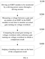
- FIG. 7 is a circuit diagram showing a judging logic for bonding-wire condition monitoring according to a specific embodiment of the present invention.
- an IGBT module condition monitoring equipment As shown in FIG. 1 , the equipment includes: an IGBT module 1 , a gate turning-on voltage overshoot monitoring module 2 , a driving circuit 3 , a bond wire state judgment module 4 and a signal acquisition module 5 .
- the gate turning-on voltage overshoot monitoring module 4 includes a voltage sampling circuit for measuring the voltage between the gate and the emitter of an IGBT in the IGBT module 1 to monitor the actual gate turning-on voltage overshoot;
- the driving circuit 3 includes a driving power source and a driving resistor, and the driving power source is connected to the gate and the emitter of the IGBT module 1 through the driving resistor;
- the bond wire state judging module 4 judges a bond wire state by judging a magnitude relationship between the actual gate turning-on voltage overshoot and a reference gate turning-on voltage overshoot threshold V g_p ;
- the signal acquisition module transmits an acquired signal to the bond wire state judgment module for setting the reference gate turning-on voltage overshoot threshold V g_p to specifically acquire information such as bus voltage, load current, and temperature.
- the IGBT module 1 is a typical large-capacity wire-bonded IGBT module, which has an internal structure as shown in FIG. 2 , and generally includes an IGBT chip 11 , a diode 12 , a solder layer 13 , an aluminum bond wire 14 , an upper copper layer 15 on a copper substrate, a ceramic layer 16 , a lower copper layer 17 on the copper substrate, a substrate 18 , and a heat sink 19 .
- the module consists of multiple IGBT chips connected in parallel. The connections among all the chips and between the chips and connection terminals are typically implemented depending on bond wires, copper plates and busbars.
- the chips are filled with transparent silicone grease with extremely low thermal conductivity coefficient, at the top.
- the power loss of the IGBT module is basically dissipated by the lower copper layer on the copper substrate through the heat sink.
- FIG. 3 is an equivalent circuit of distributed driving in consideration of the bond wires inside the IGBT.
- parasitic capacitance of the IGBT and parasitic resistance and parasitic inductance of the bond wires are considered.
- R g_on is the driving resistance
- the driving power source is connected to a gate of the IGBT internal chip via the R g_on and one bond wire
- the bond wire contains parasitic inductance L g and parasitic resistance R g .
- the collector and emitter include n bond wires, and the n bond wires contain parasitic inductance L e and parasitic resistance R e .
- a driving loop returns to a cathode of the driving power source via one bond wire of an auxiliary emitter, and the bond wire of the auxiliary emitter includes parasitic inductance L s_e and parasitic resistance R s_e . Meanwhile, the capacitance between the gate and the emitter of the IGBT is C ge , and the capacitance between the gate and the collector is C ge .
- FIG. 4 shows an equivalent circuit in consideration of multiple bond wires and parasitic capacitance inside an IGBT.
- L p_A is the parasitic inductance of each bond wire, and can be expressed as:
- L P_A 2 ⁇ 10 - 1 ⁇ l ⁇ [ ln ⁇ ( 4 ⁇ 10 3 ⁇ l d ) - 0 . 7 ⁇ 5 ] ( 1 )
- V bus is a DC bus voltage
- I L is a current which flows through a load and will flow through the collector and emitter of the IGBT after the IGBT is fully turned on.
- FIG. 5 is a schematic diagram of key waveforms (including a collector-emitter voltage ⁇ ce , a collector current i c , and a gate voltage ⁇ g ) when the IGBT is turned on.
- all the physical quantities are expressed as follows: gate current i g , gate driving voltage ⁇ g , collector-emitter voltage ⁇ ce , collector current i c , gate threshold voltage V g_th , load current I L , gate Miller voltage V g_mil , gate turning-on voltage overshoot V g_p , gate turning-on voltage V g_on , gate turning-off voltage V g_off , DC bus voltage V bus , collector turning-on current overshoot V c_max .
- the gate driving resistance is expressed as R g_on
- the gate input capacitance is expressed as C ies . According to different waveform characteristics, there are 6 phases divided.
- the gate voltage ⁇ g rises exponentially, which makes the concentration of electrons at the gate of the IGBT increase gradually.
- the collector-emitter voltage ⁇ ce and the collector current i c remain unchanged, the collector-emitter voltage ⁇ ce is the DC bus voltage V bus , and the collector current i c is zero.
- the gate begins to show a strong inversion layer.
- a gate channel begins to conduct, and the collector current i c rapidly increases from 0 to the load current I L .
- the collector-emitter voltage ⁇ ce drops slightly due to the presence of the parasitic inductance of the bus.
- Phase 3 [t 2 -t 3 ]: at the beginning of this phase, the collector current i c has risen to I L .
- the voltage of an anti-parallel diode of an upper tube starts to rise, and the collector-emitter voltage ⁇ ce starts to decrease rapidly.
- the Miller capacitance equivalent to the input capacitance is very large, so that all the gate currents i g charge the input Miller capacitance, and the voltage of the gate capacitance C gc remains unchanged as a constant gate Miller voltage V g_mil .
- the anti-parallel diode of the upper tube undergoes reverse recovery at a turning-off time. Therefore, the collector current i c will continue to rise after rising to the load current I L .
- the rising current may form a very high induced voltage, which is superimposed on the gate Miller voltage V g_mil to form the gate turning-on voltage overshoot V g_p .
- This voltage overshoot is closely related to the value of the parasitic inductance of the bond wire, so that the health state of the bond wire can be monitored by using the gate turning-on voltage overshoot.
- the gate turning-on voltage overshoot V g_p is expressed as follows (in case of operating at the same bus voltage, collector-emitter current, and temperature):
- V g_mil is a gate Miller voltage
- L p_A is parasitic inductance of each bond wire which is between an emitter of an IGBT chip and a copper busbar in the IGBT module
- n is a number of the bond wires
- m is a number of broken or detached bond wires
- L s_e is equivalent parasitic inductance of the bond wire between the emitter of the IGBT and a cathode of the driving power source
- L g is the sum parasitic inductance of the internal gate bond wire and driving resistor
- i c is a collector current.
- V g_mil V g_mil
- di c dt are related to the bus voltage, the collector-emitter current and the temperature; in case of different bus voltages, collector-emitter currents and temperatures, the gate turning-on voltage overshoot is tested in a preliminary test, and then a relationship among V g_mil ,
- di c dt as well as the bus voltage, collector-emitter current, and temperature is given by multi-point fitting or by building a data table; here, L p_A , L s_e and L g are solved by means of a physical calculation formula of inductance. In this way, the reference gate turning-on voltage overshoot thresholds V g_p corresponding to different number of lift-off bond wires in operating states at different bus voltages, collector-emitter currents and temperatures are calculated by means of the formula 3.
- a converter bus voltage (through isolated differential sampling), an IGBT load current (measured through Rogowski coil), and IGBT module temperature (through NTC and a ⁇ - ⁇ conversion circuit) can be obtained by sampling. Then, based on these signals, the reference gate turning-on voltage overshoot threshold V g_p may be set in real time with an analytical method or a look-up table method.
- di c dt of the turning-on collector current of IGBT is as high as more than 1000 A/us, therefore, as the number m of broken bond wires increases, there will be a voltage difference of several hundred millivolts or even several volts, generally.
- the calculated gate turning-on voltage overshoot V g_p can be used as a theoretical value for the reference gate turning-on voltage overshoot threshold V g_p in judging the bond wire state.
- the gate turning-on voltage overshoots are tested in a preliminary test with different voltages, currents, and temperatures, so as to determine the reference gate turning-on voltage overshoot thresholds V g_p corresponding to different numbers of broken bond wires.
- Phase 4 [t 3 -t 4 ]: At this phase, the reverse recovery current I rr of the diode starts to decrease, and the collector-emitter voltage ⁇ ce continues to decrease.
- the gate voltage V g remains at V g_mil unchanged.
- the gate voltage V g remains at V g_mil unchanged.
- Phase 6 [t 5 -t 6 ]: After the IGBT is turned on, a saturation region is entered, and the collector current i c and the collector-emitter voltage ⁇ ce remain unchanged.
- the gate power source charges the gate input capacitance to the gate turning-on voltage V g_on through the driving resistance R g_on .
- the bond wire state judging module includes a comparator and a processor; the comparator is configured to judge the magnitude relationship between the actual gate turning-on voltage overshoot and the reference gate turning-on voltage overshoot threshold V g_p and send a judging result to the processor; and the processor performs an early warning on the bond wire state according to the judging result.
- the IGBT-module condition monitoring equipment further includes latches, which are connected to outputs of the comparators and configured to perform comparison state locking on a gate turning-on voltage overshoot value, thereby guaranteeing the reversing stability at the comparison state.
- the IGBT-module condition monitoring equipment includes counters, wherein inputs of the counters are connected to outputs of the latches, and outputs of the counters are connected to the processor; and the counters are configured to record reversing numbers of different comparators for judging a probability of occurrence that a corresponding number of bond wires break.
- the processor includes a DSP or MCU, which may be configured to set the reference gate turning-on voltage overshoot threshold, receive a counting value of the counter, judge the bond wire state, perform early warning and the like.
- an IGBT-module condition monitoring method As shown in FIG. 6 , the method includes the following steps.
- an IGBT module to be monitored is driven by a driving power source through a driving resistor.
- a voltage between a gate and an emitter of an IGBT in the IGBT module is measured in real time to monitor an actual gate turning-on voltage overshoot.
- the actual gate turning-on voltage overshoot is compared with a reference gate turning-on voltage overshoot threshold to obtain a comparison result.
- the step that the actual gate turning-on voltage overshoot is compared with the reference gate turning-on voltage overshoot threshold to obtain the comparison result includes:
- n comparators wherein n is the number of bond wires, and the m-th comparator corresponds to the reference gate turning-on voltage overshoot threshold of the m broken bond wires, with m ⁇ n;
- the method further includes: setting n latches corresponding to the n comparators for latching the reversing of the corresponding comparators;
- the step of judging the bond wire state according to the comparison result includes:
- FIG. 7 shows a judging logic circuit for bonding-wire condition monitoring.
- a driving turning-on voltage signal overshoot i.e. a gate turning-on voltage overshoot signal
- the gate turning-on voltage overshoot signal is compared with a reference signal.
- the reference signal is obtained by performing an AND operation on a reference selection logic and a reference comparison setting signal.
- a reference comparison setting signal is the aforementioned reference gate turning-on voltage overshoot threshold V g_p which can be calculated by the formula 3, or obtained by testing in a preliminary test.
- the IGBTs with different number of broken bond wires correspond to different reference gate turning-on voltage overshoot thresholds V g_p .
- the reference selection logic is obtained by delaying the gate turning-on signal by one Miller platform, and the reference comparison setting signal is set on the basis of the gate turning-on voltage signal overshoot value in cases of different numbers of bond wires.
- a comparator a latch connected to an output of the comparator, a counter connected to an output of the latch, and a corresponding IGBT monitoring unit are provided for each case of bond wire breakage.
- Multiple IGBT chips are connected in parallel to form an IGBT module.
- the IGBT monitoring unit for each IGBT chip aggregates and inputs monitoring results (judging results of m broken bond wires) to the processor (specifically, a DSP or MCU may be selected), by which the bond wire state of each IGBT chip is obtained.
- the action of a high-speed comparator with a certain number indicates that the actual gate turning-on voltage overshoot of the IGBT exceeds a preset value (that is, the reference gate turning-on voltage overshoot threshold), and the bond wire is partially broken or detached (for instance, if the level of the high-speed comparator of No.
- 3 reverses to be low, 3 bond wires are indicated to be broken, the high-speed comparators with a number less than 3 may also undergo level reversing as low, and the high-speed comparators with a number greater than 3 may keep at high level).
- the outputs of the high-speed comparators are connected to the set inputs of the latches, so that the latches connected to the comparators that has undergone level reversing may undergo level reversing as high; and when a driving turning-off signal arrives, the latches are reset and the latch outputs become low. This process is repeated when the signal of the next cycle arrives. Therefore, the output signal period of the latches having the numbers corresponding to or below the number of broken bond wires is consistent with the switching period.
- the signal is output to a counter, and then the probability of the reversing is judged on the basis of the value of the counter.
- the larger the counter value the more likely the corresponding number of bond wires are broken.
- the state of the corresponding IGBT bond wires can be judged, and early warning can be made in time.
- the purpose of monitoring the state of the entire IGBT module can be achieved.
- the voltage sampling circuit in the gate voltage overshoot monitoring module is an isolation circuit, thereby ensuring the electrical isolation for strong and weak electricity and the anti-interference capability of voltage signals.
- the DSP or MCU judges the health degree of the emitter bond wires inside the IGBT module and obtains the number of broken bond wires, the IGBT module with significantly reduced health degree may be replaced, thereby reducing losses caused by the catastrophic failure of the IGBT.
- the present invention provides an IGBT-module condition monitoring equipment and method.
- the IGBT-module condition monitoring equipment includes an IGBT module, a gate turning-on voltage overshoot monitoring module, a driving circuit, a bond wire state judging module and a signal acquisition module.
- the breakage condition of bond wires is obtained by comparing a monitored actual gate turning-on voltage overshoot with a preset reference gate turning-on voltage overshoot threshold.
- the present invention solves the problem encountered in monitoring the aging of IGBT bond wires in power electronic converters.
- the slight aging of the detached bond wires can be monitored without disturbing the operation, which is high in resolution and free of invasiveness and enables real-time online monitoring at high sampling rate and low cost, showing great significance in the monitoring of the IGBT and the reliability evaluation of power electronic converters.
Landscapes
- Physics & Mathematics (AREA)
- General Physics & Mathematics (AREA)
- Engineering & Computer Science (AREA)
- Microelectronics & Electronic Packaging (AREA)
- Power Conversion In General (AREA)
- Manufacturing & Machinery (AREA)
Abstract
Description
are related to the bus voltage, the collector-emitter current and the temperature; in case of different bus voltages, collector-emitter currents and temperatures, the gate turning-on voltage overshoot is tested in a preliminary test, and then a relationship among Vg_mil
as well as the bus voltage, collector-emitter current, and temperature is given by multi-point fitting or by building a data table; and then with the
as well as the bus voltage, collector-emitter current, and temperature by multi-point fitting or by building a data table; and
wherein
are related to the bus voltage, the collector-emitter current and the temperature; in case of different bus voltages, collector-emitter currents and temperatures, the gate turning-on voltage overshoot is tested in a preliminary test, and then a relationship among Vg_mil,
as well as the bus voltage, collector-emitter current, and temperature is given by multi-point fitting or by building a data table; here, Lp_A, Ls_e and Lg are solved by means of a physical calculation formula of inductance. In this way, the reference gate turning-on voltage overshoot thresholds Vg_p corresponding to different number of lift-off bond wires in operating states at different bus voltages, collector-emitter currents and temperatures are calculated by means of the
of the turning-on collector current of IGBT is as high as more than 1000 A/us, therefore, as the number m of broken bond wires increases, there will be a voltage difference of several hundred millivolts or even several volts, generally. The calculated gate turning-on voltage overshoot Vg_p can be used as a theoretical value for the reference gate turning-on voltage overshoot threshold Vg_p in judging the bond wire state. Or, in the case of different broken bond wires of the IGBT module, the gate turning-on voltage overshoots are tested in a preliminary test with different voltages, currents, and temperatures, so as to determine the reference gate turning-on voltage overshoot thresholds Vg_p corresponding to different numbers of broken bond wires.
Claims (14)
Applications Claiming Priority (2)
| Application Number | Priority Date | Filing Date | Title |
|---|---|---|---|
| CN201910825141.X | 2019-09-03 | ||
| CN201910825141.XA CN110632490B (en) | 2019-09-03 | 2019-09-03 | An IGBT module state monitoring device and method |
Publications (2)
| Publication Number | Publication Date |
|---|---|
| US20210063466A1 US20210063466A1 (en) | 2021-03-04 |
| US11249129B2 true US11249129B2 (en) | 2022-02-15 |
Family
ID=68969996
Family Applications (1)
| Application Number | Title | Priority Date | Filing Date |
|---|---|---|---|
| US16/850,770 Active 2040-06-22 US11249129B2 (en) | 2019-09-03 | 2020-04-16 | IGBT-module condition monitoring equipment and method |
Country Status (2)
| Country | Link |
|---|---|
| US (1) | US11249129B2 (en) |
| CN (1) | CN110632490B (en) |
Cited By (1)
| Publication number | Priority date | Publication date | Assignee | Title |
|---|---|---|---|---|
| US20250012848A1 (en) * | 2021-11-23 | 2025-01-09 | Universite Gustave Eiffel | Method and device for measuring the state of health of semiconductor-based electronic components |
Families Citing this family (37)
| Publication number | Priority date | Publication date | Assignee | Title |
|---|---|---|---|---|
| CN111781482B (en) * | 2020-06-10 | 2022-10-25 | 徐州中矿大传动与自动化有限公司 | Method and device for detecting health state of bonding wire of high-power SIC MOSFET module |
| CN111856233B (en) * | 2020-07-03 | 2021-04-27 | 武汉大学 | IGBT module reliability evaluation method and device based on bond wire degradation |
| CN112730958B (en) * | 2020-12-22 | 2023-02-28 | 海光信息技术股份有限公司 | A voltage overshoot detection circuit |
| CN113131725A (en) * | 2021-04-16 | 2021-07-16 | 安徽大学 | Intelligent power module based on silicon carbide and application |
| CN113239653B (en) * | 2021-04-20 | 2022-08-12 | 武汉大学 | IGBT life prediction method and system based on composite failure mode coupling |
| US20240258901A1 (en) * | 2021-05-21 | 2024-08-01 | Hitachi Astemo, Ltd. | Gate drive circuit and power conversion device |
| CN113358996B (en) * | 2021-05-28 | 2024-03-12 | 特变电工西安柔性输配电有限公司 | Universal testing device and method for power module of flexible direct current converter valve |
| CN113406466B (en) * | 2021-06-03 | 2024-05-17 | 合肥工业大学 | IGBT module package aging on-line health management method and system |
| CN113608091B (en) * | 2021-06-28 | 2024-08-30 | 臻驱科技(上海)有限公司 | A double pulse test protection method and device |
| CN113567825B (en) * | 2021-07-26 | 2023-01-13 | 华北电力大学 | IGBT module bonding wire breakage online monitoring device, monitoring method and application |
| CN113759227B (en) * | 2021-08-24 | 2023-04-18 | 桂林电子科技大学 | Detection method of power device |
| CN114002575B (en) * | 2021-11-03 | 2024-05-24 | 华北电力大学 | A method and device for monitoring the fracture state of bonding wires of an IGBT module |
| CN114217201B (en) * | 2021-12-15 | 2022-10-18 | 中南大学 | IGBT online junction temperature measurement circuit and its measurement method |
| CN114217202A (en) * | 2021-12-16 | 2022-03-22 | 湖南大学 | An IGBT module bond wire condition monitoring and evaluation method based on multiple electrical parameters |
| CN114487683A (en) * | 2022-02-16 | 2022-05-13 | 天津理工大学 | Online monitoring method for considering aging state of inverter power device based on line voltage |
| CN114624559B (en) * | 2022-03-01 | 2025-08-08 | 格力电器(合肥)有限公司 | Testing method for welding quality of bipolar transistor |
| CN114966356B (en) * | 2022-04-29 | 2025-04-29 | 河北工业大学 | A composite relay IGBT fault detection method and detection circuit |
| CN115078942B (en) * | 2022-05-17 | 2024-10-01 | 北京交通大学 | A method for online monitoring of IGBT of converter using self-excited short circuit |
| CN114740327B (en) * | 2022-06-10 | 2022-10-11 | 江苏东海半导体股份有限公司 | IGBT module state monitoring method and device |
| CN115508683A (en) * | 2022-09-23 | 2022-12-23 | 重庆大学 | IGBT module bonding wire state detection device and detection method thereof |
| CN115616369B (en) * | 2022-10-24 | 2024-05-10 | 合肥工业大学 | Health monitoring method for bonding wires of power modules of wireless charging equipment for electric vehicles |
| CN115714138B (en) * | 2022-11-10 | 2023-08-15 | 上海功成半导体科技有限公司 | IGBT device and preparation method thereof |
| CN116203370A (en) * | 2023-01-05 | 2023-06-02 | 重庆大学 | Threshold voltage stability test method and test equipment for MOS semiconductor device |
| CN116520114A (en) * | 2023-03-09 | 2023-08-01 | 重庆大学 | MOS type semiconductor device testing equipment |
| CN117630627B (en) * | 2024-01-25 | 2024-04-26 | 广东仁懋电子有限公司 | Silicon carbide MOS device packaging detection method and system |
| CN118566676A (en) * | 2024-05-16 | 2024-08-30 | 华北电力科学研究院有限责任公司 | Method and device for determining collector-emitter voltage during IGBT turn-off delay process |
| CN118483540B (en) * | 2024-05-17 | 2025-04-15 | 北京行实科技有限公司 | An IGBT working state monitoring circuit |
| CN118378179B (en) * | 2024-06-24 | 2024-09-24 | 湖南工程学院 | Optimization and control method of distributed new energy storage network |
| CN118837701A (en) * | 2024-07-12 | 2024-10-25 | 华北电力科学研究院有限责任公司 | Method and device for monitoring rising process of IGBT short-circuit current |
| CN119199463B (en) * | 2024-11-29 | 2025-02-28 | 华北电力科学研究院有限责任公司 | IGBT internal defect location method and device based on current rise transient process |
| CN119224522B (en) * | 2024-12-03 | 2025-02-28 | 华北电力科学研究院有限责任公司 | IGBT defect detection method and device based on gate current signal in turn-on process |
| CN119666981B (en) * | 2024-12-16 | 2025-10-10 | 清华大学 | Electromagnetic soundprint monitoring method and device for IGBT module bonding wire failure status |
| CN119310430B (en) * | 2024-12-19 | 2025-03-28 | 湖南大学 | Aging separation method for converter-level power semiconductor device |
| CN119556093B (en) * | 2025-01-26 | 2025-04-15 | 成都高投芯未半导体有限公司 | IGBT device testing method and system |
| CN120446724B (en) * | 2025-05-21 | 2025-12-05 | 深圳市海思通光电科技有限公司 | An aging detection circuit for internal circuitry of a chip |
| CN120891350B (en) * | 2025-10-10 | 2025-12-09 | 山东大学 | A method, system, device and medium for measuring IGBT turn-off time |
| CN121208577B (en) * | 2025-11-28 | 2026-02-27 | 电子科技大学 | IGBT module bonding lead stripping detection method based on surface magnetic signals |
Citations (2)
| Publication number | Priority date | Publication date | Assignee | Title |
|---|---|---|---|---|
| JP2003075314A (en) * | 2001-08-31 | 2003-03-12 | Toyota Motor Corp | Wire bond joint fatigue test equipment |
| US20150002183A1 (en) * | 2012-02-24 | 2015-01-01 | Freescale Semiconductor, Inc. | Semiconductor device comprising an output driver circuitry, a packaged semiconductor device and associated methods |
Family Cites Families (6)
| Publication number | Priority date | Publication date | Assignee | Title |
|---|---|---|---|---|
| JP6056299B2 (en) * | 2012-09-13 | 2017-01-11 | 富士電機株式会社 | Semiconductor device and wire open defect detection method |
| CN102981098B (en) * | 2012-12-06 | 2015-08-05 | 天津理工大学 | A kind of IGBT module interior keys wiring faults monitoring system and method for work thereof |
| CN104880657B (en) * | 2014-02-28 | 2018-01-12 | 西安永电电气有限责任公司 | The fault detection method of IGBT device and circuit is detected accordingly |
| JP6465348B2 (en) * | 2015-02-19 | 2019-02-06 | 国立大学法人九州工業大学 | Method and apparatus for detecting bonding wire current magnetic field distribution of power semiconductor device |
| CN108256276A (en) * | 2018-03-12 | 2018-07-06 | 电子科技大学 | Power electronic device failure analysis method based on faulty physical |
| CN108627753A (en) * | 2018-05-11 | 2018-10-09 | 西安交通大学 | A kind of IGBT on-line condition monitorings method and measuring system based on Miller platform time delay |
-
2019
- 2019-09-03 CN CN201910825141.XA patent/CN110632490B/en active Active
-
2020
- 2020-04-16 US US16/850,770 patent/US11249129B2/en active Active
Patent Citations (2)
| Publication number | Priority date | Publication date | Assignee | Title |
|---|---|---|---|---|
| JP2003075314A (en) * | 2001-08-31 | 2003-03-12 | Toyota Motor Corp | Wire bond joint fatigue test equipment |
| US20150002183A1 (en) * | 2012-02-24 | 2015-01-01 | Freescale Semiconductor, Inc. | Semiconductor device comprising an output driver circuitry, a packaged semiconductor device and associated methods |
Cited By (1)
| Publication number | Priority date | Publication date | Assignee | Title |
|---|---|---|---|---|
| US20250012848A1 (en) * | 2021-11-23 | 2025-01-09 | Universite Gustave Eiffel | Method and device for measuring the state of health of semiconductor-based electronic components |
Also Published As
| Publication number | Publication date |
|---|---|
| CN110632490B (en) | 2020-11-03 |
| CN110632490A (en) | 2019-12-31 |
| US20210063466A1 (en) | 2021-03-04 |
Similar Documents
| Publication | Publication Date | Title |
|---|---|---|
| US11249129B2 (en) | IGBT-module condition monitoring equipment and method | |
| US10605854B2 (en) | Method for estimating power system health | |
| CN106443400B (en) | A method for establishing an electro-thermal-aging junction temperature calculation model for IGBT modules | |
| US12117352B2 (en) | Method, device and system for monitoring IGBT junction temperature | |
| CN108627753A (en) | A kind of IGBT on-line condition monitorings method and measuring system based on Miller platform time delay | |
| CN111781482B (en) | Method and device for detecting health state of bonding wire of high-power SIC MOSFET module | |
| Zheng et al. | Monitoring of SiC MOSFET junction temperature with on-state voltage at high currents | |
| Pu et al. | SiC MOSFET aging detection based on miller plateau voltage sensing | |
| CN111562477A (en) | On-line state monitoring and fault judging system of power semiconductor device | |
| CN114355134B (en) | Online status monitoring circuit based on power device turn-on delay time | |
| Hanif et al. | Active power cycling and condition monitoring of IGBT power modules using reflectometry | |
| Luo et al. | A fault detection method for partial chip failure in multichip IGBT modules based on turn-off delay time | |
| Hanif et al. | Degradation detection of thermally aged SiC and Si power MOSFETs using spread spectrum time domain reflectometry (SSTDR) | |
| CN113376497A (en) | Online monitoring method suitable for junction and aging information of power semiconductor device | |
| Peng et al. | A temperature-independent method for monitoring the degradation of bond wires in IGBT modules based on transfer characteristics | |
| CN115616367A (en) | Power electronic device state information online monitoring method and system | |
| Zhang et al. | In situ diagnosis of multisite wire bonding failures for multichip IGBT power modules based on crosstalk voltage | |
| Huang et al. | IGBT condition monitoring drive circuit based on self-excited short-circuit current | |
| Roy et al. | State of health (SOH) estimation of multiple switching devices using a single intelligent gate driver module | |
| Huang et al. | Research of self-excited short circuit method for monitoring IGBT health status with improved temperature criterion | |
| Shi et al. | A current sensorless IGBT junction temperature extraction method via parasitic parameters between power collector and auxiliary collector | |
| CN117074898B (en) | A SiC MOSFET junction temperature monitoring system and method for transient extreme stress | |
| Yu et al. | Determination of Short-Circuit Safe Operating Area of Trench SiC MOSFETs Under Repetitive Stress Conditions | |
| Zhang et al. | Analysis of fault precursor parameters under accelerated aging tests for IGBT modules | |
| CN118444123A (en) | IGBT fault diagnosis method based on stray inductance and concentrated voltage |
Legal Events
| Date | Code | Title | Description |
|---|---|---|---|
| AS | Assignment |
Owner name: TSINGHUA UNIVERSITY, CHINA Free format text: ASSIGNMENT OF ASSIGNORS INTEREST;ASSIGNORS:ZHANG, PINJIA;YANG, YANYONG;WANG, ZHENG;AND OTHERS;REEL/FRAME:052421/0968 Effective date: 20200408 Owner name: ENVISION ENERGY (JIANGSU) CO., LTD., CHINA Free format text: ASSIGNMENT OF ASSIGNORS INTEREST;ASSIGNORS:ZHANG, PINJIA;YANG, YANYONG;WANG, ZHENG;AND OTHERS;REEL/FRAME:052421/0968 Effective date: 20200408 Owner name: TSINGHUA UNIVERSITY, CHINA Free format text: ASSIGNMENT OF ASSIGNORS INTEREST;ASSIGNORS:TSINGHUA UNIVERSITY;ENVISION ENERGY (JIANGSU) CO., LTD.;REEL/FRAME:052429/0589 Effective date: 20200408 |
|
| FEPP | Fee payment procedure |
Free format text: ENTITY STATUS SET TO UNDISCOUNTED (ORIGINAL EVENT CODE: BIG.); ENTITY STATUS OF PATENT OWNER: SMALL ENTITY |
|
| FEPP | Fee payment procedure |
Free format text: ENTITY STATUS SET TO SMALL (ORIGINAL EVENT CODE: SMAL); ENTITY STATUS OF PATENT OWNER: SMALL ENTITY |
|
| STPP | Information on status: patent application and granting procedure in general |
Free format text: DOCKETED NEW CASE - READY FOR EXAMINATION |
|
| STPP | Information on status: patent application and granting procedure in general |
Free format text: NOTICE OF ALLOWANCE MAILED -- APPLICATION RECEIVED IN OFFICE OF PUBLICATIONS |
|
| STPP | Information on status: patent application and granting procedure in general |
Free format text: PUBLICATIONS -- ISSUE FEE PAYMENT VERIFIED |
|
| STCF | Information on status: patent grant |
Free format text: PATENTED CASE |
|
| MAFP | Maintenance fee payment |
Free format text: PAYMENT OF MAINTENANCE FEE, 4TH YR, SMALL ENTITY (ORIGINAL EVENT CODE: M2551); ENTITY STATUS OF PATENT OWNER: SMALL ENTITY Year of fee payment: 4 |