US11226403B2 - Chip-scale coherent lidar with integrated high power laser diode - Google Patents
Chip-scale coherent lidar with integrated high power laser diode Download PDFInfo
- Publication number
- US11226403B2 US11226403B2 US15/957,974 US201815957974A US11226403B2 US 11226403 B2 US11226403 B2 US 11226403B2 US 201815957974 A US201815957974 A US 201815957974A US 11226403 B2 US11226403 B2 US 11226403B2
- Authority
- US
- United States
- Prior art keywords
- signal
- mirror
- chip
- output
- master oscillator
- Prior art date
- Legal status (The legal status is an assumption and is not a legal conclusion. Google has not performed a legal analysis and makes no representation as to the accuracy of the status listed.)
- Active, expires
Links
- 230000001427 coherent effect Effects 0.000 title claims abstract description 25
- 230000005540 biological transmission Effects 0.000 claims abstract description 19
- 238000002310 reflectometry Methods 0.000 claims description 16
- 230000003287 optical effect Effects 0.000 claims description 12
- 238000000034 method Methods 0.000 claims description 10
- 239000004065 semiconductor Substances 0.000 claims description 4
- DFXZOVNXZVSTLY-UHFFFAOYSA-N [Si+4].[GeH3+]=O Chemical compound [Si+4].[GeH3+]=O DFXZOVNXZVSTLY-UHFFFAOYSA-N 0.000 claims description 3
- 238000001514 detection method Methods 0.000 description 6
- 238000010586 diagram Methods 0.000 description 6
- 230000008901 benefit Effects 0.000 description 4
- 230000009286 beneficial effect Effects 0.000 description 2
- 230000003044 adaptive effect Effects 0.000 description 1
- 238000010276 construction Methods 0.000 description 1
- 230000006870 function Effects 0.000 description 1
- 239000000463 material Substances 0.000 description 1
- 238000012986 modification Methods 0.000 description 1
- 230000004048 modification Effects 0.000 description 1
- 238000004806 packaging method and process Methods 0.000 description 1
Images


Classifications
-
- G—PHYSICS
- G01—MEASURING; TESTING
- G01S—RADIO DIRECTION-FINDING; RADIO NAVIGATION; DETERMINING DISTANCE OR VELOCITY BY USE OF RADIO WAVES; LOCATING OR PRESENCE-DETECTING BY USE OF THE REFLECTION OR RERADIATION OF RADIO WAVES; ANALOGOUS ARRANGEMENTS USING OTHER WAVES
- G01S7/00—Details of systems according to groups G01S13/00, G01S15/00, G01S17/00
- G01S7/48—Details of systems according to groups G01S13/00, G01S15/00, G01S17/00 of systems according to group G01S17/00
- G01S7/481—Constructional features, e.g. arrangements of optical elements
- G01S7/4817—Constructional features, e.g. arrangements of optical elements relating to scanning
-
- G—PHYSICS
- G01—MEASURING; TESTING
- G01S—RADIO DIRECTION-FINDING; RADIO NAVIGATION; DETERMINING DISTANCE OR VELOCITY BY USE OF RADIO WAVES; LOCATING OR PRESENCE-DETECTING BY USE OF THE REFLECTION OR RERADIATION OF RADIO WAVES; ANALOGOUS ARRANGEMENTS USING OTHER WAVES
- G01S7/00—Details of systems according to groups G01S13/00, G01S15/00, G01S17/00
- G01S7/48—Details of systems according to groups G01S13/00, G01S15/00, G01S17/00 of systems according to group G01S17/00
- G01S7/481—Constructional features, e.g. arrangements of optical elements
- G01S7/4814—Constructional features, e.g. arrangements of optical elements of transmitters alone
- G01S7/4815—Constructional features, e.g. arrangements of optical elements of transmitters alone using multiple transmitters
-
- B—PERFORMING OPERATIONS; TRANSPORTING
- B81—MICROSTRUCTURAL TECHNOLOGY
- B81B—MICROSTRUCTURAL DEVICES OR SYSTEMS, e.g. MICROMECHANICAL DEVICES
- B81B7/00—Microstructural systems; Auxiliary parts of microstructural devices or systems
- B81B7/02—Microstructural systems; Auxiliary parts of microstructural devices or systems containing distinct electrical or optical devices of particular relevance for their function, e.g. microelectro-mechanical systems [MEMS]
-
- G—PHYSICS
- G01—MEASURING; TESTING
- G01S—RADIO DIRECTION-FINDING; RADIO NAVIGATION; DETERMINING DISTANCE OR VELOCITY BY USE OF RADIO WAVES; LOCATING OR PRESENCE-DETECTING BY USE OF THE REFLECTION OR RERADIATION OF RADIO WAVES; ANALOGOUS ARRANGEMENTS USING OTHER WAVES
- G01S17/00—Systems using the reflection or reradiation of electromagnetic waves other than radio waves, e.g. lidar systems
- G01S17/003—Bistatic lidar systems; Multistatic lidar systems
-
- G—PHYSICS
- G01—MEASURING; TESTING
- G01S—RADIO DIRECTION-FINDING; RADIO NAVIGATION; DETERMINING DISTANCE OR VELOCITY BY USE OF RADIO WAVES; LOCATING OR PRESENCE-DETECTING BY USE OF THE REFLECTION OR RERADIATION OF RADIO WAVES; ANALOGOUS ARRANGEMENTS USING OTHER WAVES
- G01S17/00—Systems using the reflection or reradiation of electromagnetic waves other than radio waves, e.g. lidar systems
- G01S17/02—Systems using the reflection of electromagnetic waves other than radio waves
- G01S17/06—Systems determining position data of a target
- G01S17/08—Systems determining position data of a target for measuring distance only
- G01S17/32—Systems determining position data of a target for measuring distance only using transmission of continuous waves, whether amplitude-, frequency-, or phase-modulated, or unmodulated
- G01S17/34—Systems determining position data of a target for measuring distance only using transmission of continuous waves, whether amplitude-, frequency-, or phase-modulated, or unmodulated using transmission of continuous, frequency-modulated waves while heterodyning the received signal, or a signal derived therefrom, with a locally-generated signal related to the contemporaneously transmitted signal
-
- G—PHYSICS
- G01—MEASURING; TESTING
- G01S—RADIO DIRECTION-FINDING; RADIO NAVIGATION; DETERMINING DISTANCE OR VELOCITY BY USE OF RADIO WAVES; LOCATING OR PRESENCE-DETECTING BY USE OF THE REFLECTION OR RERADIATION OF RADIO WAVES; ANALOGOUS ARRANGEMENTS USING OTHER WAVES
- G01S17/00—Systems using the reflection or reradiation of electromagnetic waves other than radio waves, e.g. lidar systems
- G01S17/02—Systems using the reflection of electromagnetic waves other than radio waves
- G01S17/06—Systems determining position data of a target
- G01S17/42—Simultaneous measurement of distance and other co-ordinates
-
- G—PHYSICS
- G01—MEASURING; TESTING
- G01S—RADIO DIRECTION-FINDING; RADIO NAVIGATION; DETERMINING DISTANCE OR VELOCITY BY USE OF RADIO WAVES; LOCATING OR PRESENCE-DETECTING BY USE OF THE REFLECTION OR RERADIATION OF RADIO WAVES; ANALOGOUS ARRANGEMENTS USING OTHER WAVES
- G01S17/00—Systems using the reflection or reradiation of electromagnetic waves other than radio waves, e.g. lidar systems
- G01S17/02—Systems using the reflection of electromagnetic waves other than radio waves
- G01S17/50—Systems of measurement based on relative movement of target
- G01S17/58—Velocity or trajectory determination systems; Sense-of-movement determination systems
-
- G—PHYSICS
- G01—MEASURING; TESTING
- G01S—RADIO DIRECTION-FINDING; RADIO NAVIGATION; DETERMINING DISTANCE OR VELOCITY BY USE OF RADIO WAVES; LOCATING OR PRESENCE-DETECTING BY USE OF THE REFLECTION OR RERADIATION OF RADIO WAVES; ANALOGOUS ARRANGEMENTS USING OTHER WAVES
- G01S17/00—Systems using the reflection or reradiation of electromagnetic waves other than radio waves, e.g. lidar systems
- G01S17/86—Combinations of lidar systems with systems other than lidar, radar or sonar, e.g. with direction finders
-
- G—PHYSICS
- G01—MEASURING; TESTING
- G01S—RADIO DIRECTION-FINDING; RADIO NAVIGATION; DETERMINING DISTANCE OR VELOCITY BY USE OF RADIO WAVES; LOCATING OR PRESENCE-DETECTING BY USE OF THE REFLECTION OR RERADIATION OF RADIO WAVES; ANALOGOUS ARRANGEMENTS USING OTHER WAVES
- G01S17/00—Systems using the reflection or reradiation of electromagnetic waves other than radio waves, e.g. lidar systems
- G01S17/88—Lidar systems specially adapted for specific applications
- G01S17/93—Lidar systems specially adapted for specific applications for anti-collision purposes
- G01S17/931—Lidar systems specially adapted for specific applications for anti-collision purposes of land vehicles
-
- G—PHYSICS
- G01—MEASURING; TESTING
- G01S—RADIO DIRECTION-FINDING; RADIO NAVIGATION; DETERMINING DISTANCE OR VELOCITY BY USE OF RADIO WAVES; LOCATING OR PRESENCE-DETECTING BY USE OF THE REFLECTION OR RERADIATION OF RADIO WAVES; ANALOGOUS ARRANGEMENTS USING OTHER WAVES
- G01S7/00—Details of systems according to groups G01S13/00, G01S15/00, G01S17/00
- G01S7/48—Details of systems according to groups G01S13/00, G01S15/00, G01S17/00 of systems according to group G01S17/00
- G01S7/481—Constructional features, e.g. arrangements of optical elements
- G01S7/4816—Constructional features, e.g. arrangements of optical elements of receivers alone
-
- G—PHYSICS
- G01—MEASURING; TESTING
- G01S—RADIO DIRECTION-FINDING; RADIO NAVIGATION; DETERMINING DISTANCE OR VELOCITY BY USE OF RADIO WAVES; LOCATING OR PRESENCE-DETECTING BY USE OF THE REFLECTION OR RERADIATION OF RADIO WAVES; ANALOGOUS ARRANGEMENTS USING OTHER WAVES
- G01S7/00—Details of systems according to groups G01S13/00, G01S15/00, G01S17/00
- G01S7/48—Details of systems according to groups G01S13/00, G01S15/00, G01S17/00 of systems according to group G01S17/00
- G01S7/481—Constructional features, e.g. arrangements of optical elements
- G01S7/4818—Constructional features, e.g. arrangements of optical elements using optical fibres
-
- G—PHYSICS
- G01—MEASURING; TESTING
- G01S—RADIO DIRECTION-FINDING; RADIO NAVIGATION; DETERMINING DISTANCE OR VELOCITY BY USE OF RADIO WAVES; LOCATING OR PRESENCE-DETECTING BY USE OF THE REFLECTION OR RERADIATION OF RADIO WAVES; ANALOGOUS ARRANGEMENTS USING OTHER WAVES
- G01S7/00—Details of systems according to groups G01S13/00, G01S15/00, G01S17/00
- G01S7/48—Details of systems according to groups G01S13/00, G01S15/00, G01S17/00 of systems according to group G01S17/00
- G01S7/491—Details of non-pulse systems
- G01S7/4911—Transmitters
-
- G—PHYSICS
- G01—MEASURING; TESTING
- G01S—RADIO DIRECTION-FINDING; RADIO NAVIGATION; DETERMINING DISTANCE OR VELOCITY BY USE OF RADIO WAVES; LOCATING OR PRESENCE-DETECTING BY USE OF THE REFLECTION OR RERADIATION OF RADIO WAVES; ANALOGOUS ARRANGEMENTS USING OTHER WAVES
- G01S7/00—Details of systems according to groups G01S13/00, G01S15/00, G01S17/00
- G01S7/48—Details of systems according to groups G01S13/00, G01S15/00, G01S17/00 of systems according to group G01S17/00
- G01S7/491—Details of non-pulse systems
- G01S7/4912—Receivers
- G01S7/4913—Circuits for detection, sampling, integration or read-out
- G01S7/4914—Circuits for detection, sampling, integration or read-out of detector arrays, e.g. charge-transfer gates
-
- G—PHYSICS
- G01—MEASURING; TESTING
- G01S—RADIO DIRECTION-FINDING; RADIO NAVIGATION; DETERMINING DISTANCE OR VELOCITY BY USE OF RADIO WAVES; LOCATING OR PRESENCE-DETECTING BY USE OF THE REFLECTION OR RERADIATION OF RADIO WAVES; ANALOGOUS ARRANGEMENTS USING OTHER WAVES
- G01S7/00—Details of systems according to groups G01S13/00, G01S15/00, G01S17/00
- G01S7/48—Details of systems according to groups G01S13/00, G01S15/00, G01S17/00 of systems according to group G01S17/00
- G01S7/497—Means for monitoring or calibrating
- G01S7/4972—Alignment of sensor
-
- G—PHYSICS
- G01—MEASURING; TESTING
- G01S—RADIO DIRECTION-FINDING; RADIO NAVIGATION; DETERMINING DISTANCE OR VELOCITY BY USE OF RADIO WAVES; LOCATING OR PRESENCE-DETECTING BY USE OF THE REFLECTION OR RERADIATION OF RADIO WAVES; ANALOGOUS ARRANGEMENTS USING OTHER WAVES
- G01S7/00—Details of systems according to groups G01S13/00, G01S15/00, G01S17/00
- G01S7/48—Details of systems according to groups G01S13/00, G01S15/00, G01S17/00 of systems according to group G01S17/00
- G01S7/499—Details of systems according to groups G01S13/00, G01S15/00, G01S17/00 of systems according to group G01S17/00 using polarisation effects
-
- G—PHYSICS
- G02—OPTICS
- G02B—OPTICAL ELEMENTS, SYSTEMS OR APPARATUS
- G02B27/00—Optical systems or apparatus not provided for by any of the groups G02B1/00 - G02B26/00, G02B30/00
- G02B27/28—Optical systems or apparatus not provided for by any of the groups G02B1/00 - G02B26/00, G02B30/00 for polarising
-
- G—PHYSICS
- G02—OPTICS
- G02B—OPTICAL ELEMENTS, SYSTEMS OR APPARATUS
- G02B27/00—Optical systems or apparatus not provided for by any of the groups G02B1/00 - G02B26/00, G02B30/00
- G02B27/30—Collimators
-
- G—PHYSICS
- G02—OPTICS
- G02B—OPTICAL ELEMENTS, SYSTEMS OR APPARATUS
- G02B6/00—Light guides; Structural details of arrangements comprising light guides and other optical elements, e.g. couplings
- G02B6/10—Light guides; Structural details of arrangements comprising light guides and other optical elements, e.g. couplings of the optical waveguide type
- G02B6/12—Light guides; Structural details of arrangements comprising light guides and other optical elements, e.g. couplings of the optical waveguide type of the integrated circuit kind
- G02B6/122—Basic optical elements, e.g. light-guiding paths
-
- G—PHYSICS
- G02—OPTICS
- G02B—OPTICAL ELEMENTS, SYSTEMS OR APPARATUS
- G02B6/00—Light guides; Structural details of arrangements comprising light guides and other optical elements, e.g. couplings
- G02B6/24—Coupling light guides
- G02B6/26—Optical coupling means
- G02B6/27—Optical coupling means with polarisation selective and adjusting means
- G02B6/2753—Optical coupling means with polarisation selective and adjusting means characterised by their function or use, i.e. of the complete device
- G02B6/2766—Manipulating the plane of polarisation from one input polarisation to another output polarisation, e.g. polarisation rotators, linear to circular polarisation converters
-
- G—PHYSICS
- G02—OPTICS
- G02B—OPTICAL ELEMENTS, SYSTEMS OR APPARATUS
- G02B6/00—Light guides; Structural details of arrangements comprising light guides and other optical elements, e.g. couplings
- G02B6/24—Coupling light guides
- G02B6/42—Coupling light guides with opto-electronic elements
- G02B6/4201—Packages, e.g. shape, construction, internal or external details
- G02B6/4204—Packages, e.g. shape, construction, internal or external details the coupling comprising intermediate optical elements, e.g. lenses, holograms
- G02B6/4207—Packages, e.g. shape, construction, internal or external details the coupling comprising intermediate optical elements, e.g. lenses, holograms with optical elements reducing the sensitivity to optical feedback
- G02B6/4208—Packages, e.g. shape, construction, internal or external details the coupling comprising intermediate optical elements, e.g. lenses, holograms with optical elements reducing the sensitivity to optical feedback using non-reciprocal elements or birefringent plates, i.e. quasi-isolators
- G02B6/4209—Optical features
-
- H—ELECTRICITY
- H01—ELECTRIC ELEMENTS
- H01L—SEMICONDUCTOR DEVICES NOT COVERED BY CLASS H10
- H01L23/00—Details of semiconductor or other solid state devices
- H01L23/544—Marks applied to semiconductor devices or parts, e.g. registration marks, alignment structures, wafer maps
-
- H—ELECTRICITY
- H01—ELECTRIC ELEMENTS
- H01L—SEMICONDUCTOR DEVICES NOT COVERED BY CLASS H10
- H01L31/00—Semiconductor devices sensitive to infrared radiation, light, electromagnetic radiation of shorter wavelength or corpuscular radiation and specially adapted either for the conversion of the energy of such radiation into electrical energy or for the control of electrical energy by such radiation; Processes or apparatus specially adapted for the manufacture or treatment thereof or of parts thereof; Details thereof
- H01L31/02—Details
- H01L31/0232—Optical elements or arrangements associated with the device
- H01L31/02327—Optical elements or arrangements associated with the device the optical elements being integrated or being directly associated to the device, e.g. back reflectors
-
- H—ELECTRICITY
- H01—ELECTRIC ELEMENTS
- H01L—SEMICONDUCTOR DEVICES NOT COVERED BY CLASS H10
- H01L31/00—Semiconductor devices sensitive to infrared radiation, light, electromagnetic radiation of shorter wavelength or corpuscular radiation and specially adapted either for the conversion of the energy of such radiation into electrical energy or for the control of electrical energy by such radiation; Processes or apparatus specially adapted for the manufacture or treatment thereof or of parts thereof; Details thereof
- H01L31/12—Semiconductor devices sensitive to infrared radiation, light, electromagnetic radiation of shorter wavelength or corpuscular radiation and specially adapted either for the conversion of the energy of such radiation into electrical energy or for the control of electrical energy by such radiation; Processes or apparatus specially adapted for the manufacture or treatment thereof or of parts thereof; Details thereof structurally associated with, e.g. formed in or on a common substrate with, one or more electric light sources, e.g. electroluminescent light sources, and electrically or optically coupled thereto
- H01L31/16—Semiconductor devices sensitive to infrared radiation, light, electromagnetic radiation of shorter wavelength or corpuscular radiation and specially adapted either for the conversion of the energy of such radiation into electrical energy or for the control of electrical energy by such radiation; Processes or apparatus specially adapted for the manufacture or treatment thereof or of parts thereof; Details thereof structurally associated with, e.g. formed in or on a common substrate with, one or more electric light sources, e.g. electroluminescent light sources, and electrically or optically coupled thereto the semiconductor device sensitive to radiation being controlled by the light source or sources
-
- H—ELECTRICITY
- H01—ELECTRIC ELEMENTS
- H01S—DEVICES USING THE PROCESS OF LIGHT AMPLIFICATION BY STIMULATED EMISSION OF RADIATION [LASER] TO AMPLIFY OR GENERATE LIGHT; DEVICES USING STIMULATED EMISSION OF ELECTROMAGNETIC RADIATION IN WAVE RANGES OTHER THAN OPTICAL
- H01S5/00—Semiconductor lasers
- H01S5/10—Construction or shape of the optical resonator, e.g. extended or external cavity, coupled cavities, bent-guide, varying width, thickness or composition of the active region
- H01S5/12—Construction or shape of the optical resonator, e.g. extended or external cavity, coupled cavities, bent-guide, varying width, thickness or composition of the active region the resonator having a periodic structure, e.g. in distributed feedback [DFB] lasers
- H01S5/125—Distributed Bragg reflector [DBR] lasers
-
- B—PERFORMING OPERATIONS; TRANSPORTING
- B81—MICROSTRUCTURAL TECHNOLOGY
- B81B—MICROSTRUCTURAL DEVICES OR SYSTEMS, e.g. MICROMECHANICAL DEVICES
- B81B2207/00—Microstructural systems or auxiliary parts thereof
- B81B2207/03—Electronic circuits for micromechanical devices which are not application specific, e.g. for controlling, power supplying, testing, protecting
-
- G—PHYSICS
- G02—OPTICS
- G02B—OPTICAL ELEMENTS, SYSTEMS OR APPARATUS
- G02B6/00—Light guides; Structural details of arrangements comprising light guides and other optical elements, e.g. couplings
- G02B2006/0098—Light guides; Structural details of arrangements comprising light guides and other optical elements, e.g. couplings for scanning
-
- H—ELECTRICITY
- H01—ELECTRIC ELEMENTS
- H01L—SEMICONDUCTOR DEVICES NOT COVERED BY CLASS H10
- H01L2223/00—Details relating to semiconductor or other solid state devices covered by the group H01L23/00
- H01L2223/544—Marks applied to semiconductor devices or parts
- H01L2223/54426—Marks applied to semiconductor devices or parts for alignment
-
- H—ELECTRICITY
- H01—ELECTRIC ELEMENTS
- H01L—SEMICONDUCTOR DEVICES NOT COVERED BY CLASS H10
- H01L2223/00—Details relating to semiconductor or other solid state devices covered by the group H01L23/00
- H01L2223/544—Marks applied to semiconductor devices or parts
- H01L2223/54473—Marks applied to semiconductor devices or parts for use after dicing
- H01L2223/54486—Located on package parts, e.g. encapsulation, leads, package substrate
Definitions
- the subject disclosure relates to chip-scale coherent lidar with an integrated high power laser diode.
- Vehicles e.g., automobiles, trucks, construction equipment, farm equipment, automated factory equipment
- sensors that provide information to augment or automate vehicle operation.
- exemplary sensors include radio detection and ranging (radar) systems, cameras, microphones, and light detection and ranging (lidar) systems.
- An exemplary lidar system is a coherent lidar system that transmits a frequency modulated continuous wave (FMCW) signal and relies on optical coherence between the transmitted signal and a return signal resulting from reflected scattering of the transmitted signal by a target to perform detection of the target.
- FMCW frequency modulated continuous wave
- reducing the size and cost of the lidar system may be beneficial. Accordingly, it is desirable to provide a chip-scale coherent lidar with an integrated high power laser diode.
- a chip-scale coherent lidar system includes a master oscillator integrated on a chip to simultaneously provide a signal for transmission and a local oscillator (LO) signal.
- the system also includes a beam steering device to direct an output signal obtained from the signal for transmission out of the system, and a combiner on the chip to combine the LO signal and a return signal resulting from a reflection of the output signal by a target.
- One or more photodetectors obtain a result of interference between the LO signal and the return signal to determine information about the target.
- the master oscillator includes a gain medium that is modulated by a current source to provide a frequency modulated continuous wave (FMCW) signal.
- FMCW frequency modulated continuous wave
- the current source is off the chip.
- the master oscillator also includes a first mirror to output the signal for transmission and a second mirror to output the LO signal, and the system also includes an amplifier to amplify the signal for transmission to produce the output signal.
- the first mirror is a low-reflectivity mirror and the second mirror is a high-reflectivity mirror.
- a reflectivity of the first mirror is 5-10 percent, and the reflectivity of the second mirror is 80-90 percent.
- the amplifier is a semiconductor optical amplifier on the chip with an off-chip current source.
- the output signal has an output power on the order of 500 milliwatts (mW) and the LO signal has an output power on the order of 5 mW.
- the master oscillator is a distributed Bragg reflector laser diode (DBR-LD).
- DBR-LD distributed Bragg reflector laser diode
- the one or more photodetectors is a germanium-on-silicon (Ge-on-Si) photodetectors.
- system is a monostatic system and further comprises a circulator.
- system is bistatic.
- system is within or on a vehicle and detects a location and speed of an object relative to the vehicle.
- a method of assembling a coherent lidar system includes integrating a master oscillator and an optical amplifier on a chip to simultaneously provide an output signal and a local oscillator (LO) signal.
- the master oscillator includes a gain medium, a first mirror, and a second mirror.
- the method also includes arranging a first current source to supply the gain medium and a second current source to supply the optical amplifier.
- the method also includes arranging the first mirror to pass through a transmit signal from the gain medium to the optical amplifier and arranging the second mirror to pass through the LO signal from the gain medium.
- the method also includes configuring the first current source to modulate a frequency of the gain medium.
- a vehicle in yet another exemplary embodiment, includes a chip-scale coherent lidar system.
- the system includes a master oscillator integrated on a chip to simultaneously provide a signal for transmission and a local oscillator (LO) signal.
- the system also includes a beam steering device to direct an output signal obtained from the signal for transmission out of the system, and a combiner on the chip to combine the LO signal and a return signal resulting from a reflection of the output signal by a target.
- One or more photodetectors obtain a result of interference between the LO signal and the return signal to determine information about the target.
- the vehicle also includes a controller to augment or automate operation of the vehicle based on information obtained from the return signal in the lidar system.
- the master oscillator includes a gain medium that is modulated by a current source to provide a frequency modulated continuous wave (FMCW) signal.
- FMCW frequency modulated continuous wave
- the master oscillator also includes a first mirror to output the signal for transmission and a second mirror to output the LO signal, and the system also includes an amplifier to amplify the signal for transmission to produce the output signal.
- the first mirror is a low-reflectivity mirror and the second mirror is a high-reflectivity mirror.
- FIG. 1 is a block diagram of a scenario involving a chip-scale coherent lidar system with an integrated high power laser diode according to one or more embodiments;
- FIG. 2 is a block diagram of an on-chip coherent lidar system according to one or more embodiments
- FIG. 3 is a block diagram of an on-chip coherent lidar system according to alternate one or more embodiments.
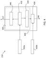
- FIG. 4 details the light source of the lidar system according to one or more embodiments.
- a coherent lidar system may be one of the sensors used to augment or automate vehicle operation. In applications like object detection in a vehicle, compactness in the arrangement and packaging of the components is beneficial.
- a chip-scale lidar may be preferred to achieve this objective. Although not all components of the chip-scale coherent lidar are integrated, it is highly desirable to integrate the high power laser diode optical source with the lidar photonic chip.
- Embodiments of the systems and methods detailed herein relate to chip-scale coherent lidar with an integrated high power laser diode.
- the high power laser facilitates long range lidar applications (e.g., over 100 meters).
- FIG. 1 is a block diagram of a scenario involving a chip-scale coherent lidar system 110 with an integrated high power laser diode.
- the vehicle 100 shown in FIG. 1 is an automobile 101 .
- a coherent lidar system 110 is shown on the roof of the automobile 101 .
- one or more lidar systems 110 may be located elsewhere on the vehicle 100 .
- Another sensor 115 e.g., camera, sonar, radar system
- Information obtained by the lidar system 110 and one or more other sensors 115 may be provided to a controller 120 (e.g., electronic control unit (ECU)) for image or data processing, target recognition, and subsequent vehicle control.
- ECU electronice control unit
- the controller 120 may use the information to control one or more vehicle systems 130 .
- the vehicle 100 may be an autonomous vehicle and the controller 120 may perform known vehicle operational control using information from the lidar system 110 and other sources.
- the controller 120 may augment vehicle operation using information from the lidar system 110 and other sources as part of a known system (e.g., collision avoidance system, adaptive cruise control system).
- the lidar system 110 and one or more other sensors 115 may be used to detect objects 140 , such as the pedestrian 145 shown in FIG. 1 .
- the controller 120 may include processing circuitry that may include an application specific integrated circuit (ASIC), an electronic circuit, a processor (shared, dedicated, or group) and memory that executes one or more software or firmware programs, a combinational logic circuit, and/or other suitable components that provide the described functionality.
- ASIC application specific integrated circuit
- ASIC application specific integrated circuit
- processor shared, dedicated, or group
- memory that executes one or more software or firmware programs, a combinational logic circuit, and/or other suitable components that provide the described functionality.
- FIG. 2 is a block diagram of an on-chip coherent lidar system 110 according to one or more embodiments.
- the exemplary lidar system 110 shown in FIG. 2 is a monostatic system that uses a circulator 225 to facilitate the use of the same aperture lens 200 for light output from the lidar system 110 as an output signal 240 and light obtained by the lidar system 110 as a receive beam 250 .
- a beam steering device 220 may be implemented as a scanning mirror actuated by microelectromechanical systems (MEMS) (i.e., a MEMS scanning mirror) that is used to direct the output signal 240 out of the lidar system 110 and direct the receive beam 250 to the circulator 225 .
- MEMS microelectromechanical systems
- the lidar system 110 includes a light source 210 , which is an integrated laser diode that is detailed with reference to FIG. 4 .
- the light source 210 outputs the output signal 240 and also outputs a local oscillator (LO) signal 217 via a spot size converter (SSC) 215 .
- the SSC 215 couples the LO signal 217 to a planar on-chip waveguide.
- the output signal 240 from the lidar system 110 is scattered by the target 140 . Some of that scattered light reenters the lidar system 110 as a receive beam 250 .
- the receive beam 250 enters the aperture lens 200 and is directed, by the beam steering device 220 , to the circulator 225 .
- a second SSC 230 couples the incoming receive beam 250 to a planar waveguide.
- the LO signal 217 and the receive beam 250 are both input to a combiner 260 .
- the combined signal 265 is then split to two photodetectors 270 a , 270 b (generally referred to as 270 ).
- the photodetectors 270 may be dual-balanced germanium-on-silicon (Ge-on-Si) photodetectors, for example.
- the LO signal 217 and receive beam 250 in the combined signal 265 interfere with each other and a resulting radio frequency (RF) beat signal is detected by each of the photodetectors 270 .
- the interference between the receive beam 250 and the LO signal 217 results in a coherent combination of the two beams.
- the lidar system 110 is referred to as a coherent lidar system, unlike a time-of-flight system, for example, in which direct detection of the receive beam is obtained.
- the interference in each photodetector 270 results in the RF beat signal which facilitates identification of a time-delayed receive beam 250 that resulted from the output signal 240 . This prevents errant light from another light source outside the lidar system 110 that is within the field of view of the lidar system 110 from being mistaken for a receive beam 250 that is reflected by a target 140 .
- the photodetectors 270 are semiconductor devices that convert the result of the interference between the receive beam 250 and the LO signal 217 into electrical currents 275 a , 275 b (generally referred to as 275 ). These electrical currents 275 are also referred to as beat signals.
- the two photodetectors 270 are used in accordance with a known balanced detector technique to cancel intensity noise in the LO signal 217 (which is caused by the light source 210 and, thus, is the same in the output signal 240 ) that is common to both photodetectors 270 .
- the electrical currents 275 from each of the photodetectors 270 are combined and processed to obtain three-dimensional information like range to the target 140 and the relative speed of the target 140 to the lidar system 110 as a function of two-dimensional spatial coordinates.
- the processing may be performed within the lidar system 110 by a processor 280 or outside the lidar system 110 by the controller 120 , for example.
- the processor 280 may include processing circuitry similar to that discussed for the controller 120 .
- FIG. 3 is a block diagram of an on-chip coherent lidar system 110 according to alternate one or more embodiments.
- a bistatic lidar system 110 is shown in the exemplary embodiment of FIG. 3 .
- Most of the bistatic lidar system 110 , shown in FIG. 3 is similar to the monostatic lidar system 110 , shown in FIG. 2 .
- the components detailed with reference to FIG. 2 are not discussed again.
- the primary difference between the monostatic and bistatic systems is in the inclusion, in the bistatic system, of separate beam steering devices 220 a , 220 b (generally referred to as 220 ) and aperture lenses 200 a , 200 b (generally referred to as 200 ) for the output signal 240 and receive beam 250 .
- a circulator 250 is not needed in the bistatic system of FIG. 3 .
- FIG. 4 details the light source 210 of the lidar system 110 according to one or more embodiments.
- the light source 210 is a chip-scale integrated high power laser diode.
- the light source 210 is a high power narrow linewidth light source.
- the light source 210 includes components that are integrated on a chip 400 and current sources 450 a , 450 b (generally referred to as 450 ) that are not on the chip 400 .
- the current sources 450 may also be integrated on the chip.
- the light source 210 is in a master oscillator-power amplifier (MOPA) laser configuration.
- MOPA master oscillator-power amplifier
- the master oscillator 405 may be a distributed Bragg Reflector (DBR) laser diode (LD) in the exemplary embodiment shown in FIG. 4 .
- the master oscillator 405 includes a gain medium 410 (i.e., laser medium) powered by the current source 450 a , and two DBR mirrors (output-side mirror 420 and LO-side mirror 440 ).
- the power amplifier 430 may be a semiconductor optical amplifier (SOA) powered by the current source 450 b .
- SOA semiconductor optical amplifier
- the modulation of the current source 450 a results in the frequency modulation of the output signal 240 and the LO signal 217 .
- controlling the current source 450 a facilitates outputting an FMCW signal from the master oscillator 405 .
- the master oscillator 405 is a laser cavity including the gain medium 410 the output-side mirror 420 as a low-reflectivity mirror (e.g. reflectivity of 5-10 percent) and the LO-side mirror 440 as a high reflectivity mirror (e.g., reflectivity of 80-90 percent).
- the amplifier 430 e.g., SOA
- the amplifier 430 amplifies the output of the master oscillator 405 that passes through the output-side mirror 420 without compromising its linewidth.
- the resulting output signal 240 constitutes the transmit light before exiting the lidar system 110 .
- the output of the master oscillator 405 that passes through the LO-side mirror 440 is the LO signal 217 that is used for coherent detection.
- the light source 210 provides both the output signal 240 and LO signal 217 simultaneously.
- the output signal 240 may have output power on the order of 500 milliwatt (mW) while the LO signal 217 has output power on the order of 5 mW.
- the light source 210 may include a tapered DBR laser diode rather than a combination of a master oscillator 405 and the amplifier 430 .
Abstract
Description
Claims (19)
Priority Applications (3)
| Application Number | Priority Date | Filing Date | Title |
|---|---|---|---|
| US15/957,974 US11226403B2 (en) | 2017-07-12 | 2018-04-20 | Chip-scale coherent lidar with integrated high power laser diode |
| CN201910261645.3A CN110389329A (en) | 2017-07-12 | 2019-04-02 | Chip-scale coherent laser radar with integrated high power laser diode |
| DE102019109649.9A DE102019109649A1 (en) | 2017-07-12 | 2019-04-11 | COHERENT LIDAR IN CHIP SIZE WITH INTEGRATED HIGH PERFORMANCE LASER DIODE |
Applications Claiming Priority (2)
| Application Number | Priority Date | Filing Date | Title |
|---|---|---|---|
| US201762531414P | 2017-07-12 | 2017-07-12 | |
| US15/957,974 US11226403B2 (en) | 2017-07-12 | 2018-04-20 | Chip-scale coherent lidar with integrated high power laser diode |
Publications (2)
| Publication Number | Publication Date |
|---|---|
| US20190018139A1 US20190018139A1 (en) | 2019-01-17 |
| US11226403B2 true US11226403B2 (en) | 2022-01-18 |
Family
ID=64998803
Family Applications (9)
| Application Number | Title | Priority Date | Filing Date |
|---|---|---|---|
| US15/957,974 Active 2040-11-19 US11226403B2 (en) | 2017-07-12 | 2018-04-20 | Chip-scale coherent lidar with integrated high power laser diode |
| US16/017,278 Active 2039-08-21 US10914821B2 (en) | 2017-07-12 | 2018-06-25 | Calibration and alignment of coherent lidar system |
| US16/018,831 Active 2039-08-12 US11002832B2 (en) | 2017-07-12 | 2018-06-26 | Chip-scale LIDAR with a single 2D MEMS scanner |
| US16/018,716 Active 2039-08-21 US10914822B2 (en) | 2017-07-12 | 2018-06-26 | Dual-laser chip-scale lidar for simultaneous range-doppler sensing |
| US16/018,730 Active 2039-08-21 US10976414B2 (en) | 2017-07-12 | 2018-06-26 | Heterogeneous integration of curved mirror structure for passive alignment in chip-scale lidar |
| US16/019,691 Active US10564263B2 (en) | 2017-07-12 | 2018-06-27 | Chip-scale LIDAR with a single MEMS scanner in a compact optical package |
| US16/019,686 Abandoned US20190018198A1 (en) | 2017-07-12 | 2018-06-27 | Photonic integrated circuit edge coupler structure with reduced reflection for integrated laser diodes |
| US16/020,214 Active 2039-11-29 US11092671B2 (en) | 2017-07-12 | 2018-06-27 | Laser diode optical frequency modulation linearization algorithm |
| US16/020,202 Active 2039-12-05 US11067670B2 (en) | 2017-07-12 | 2018-06-27 | Heterogeneously integrated chip-scale lidar system |
Family Applications After (8)
| Application Number | Title | Priority Date | Filing Date |
|---|---|---|---|
| US16/017,278 Active 2039-08-21 US10914821B2 (en) | 2017-07-12 | 2018-06-25 | Calibration and alignment of coherent lidar system |
| US16/018,831 Active 2039-08-12 US11002832B2 (en) | 2017-07-12 | 2018-06-26 | Chip-scale LIDAR with a single 2D MEMS scanner |
| US16/018,716 Active 2039-08-21 US10914822B2 (en) | 2017-07-12 | 2018-06-26 | Dual-laser chip-scale lidar for simultaneous range-doppler sensing |
| US16/018,730 Active 2039-08-21 US10976414B2 (en) | 2017-07-12 | 2018-06-26 | Heterogeneous integration of curved mirror structure for passive alignment in chip-scale lidar |
| US16/019,691 Active US10564263B2 (en) | 2017-07-12 | 2018-06-27 | Chip-scale LIDAR with a single MEMS scanner in a compact optical package |
| US16/019,686 Abandoned US20190018198A1 (en) | 2017-07-12 | 2018-06-27 | Photonic integrated circuit edge coupler structure with reduced reflection for integrated laser diodes |
| US16/020,214 Active 2039-11-29 US11092671B2 (en) | 2017-07-12 | 2018-06-27 | Laser diode optical frequency modulation linearization algorithm |
| US16/020,202 Active 2039-12-05 US11067670B2 (en) | 2017-07-12 | 2018-06-27 | Heterogeneously integrated chip-scale lidar system |
Country Status (3)
| Country | Link |
|---|---|
| US (9) | US11226403B2 (en) |
| CN (9) | CN109254278B (en) |
| DE (2) | DE102019109649A1 (en) |
Families Citing this family (45)
| Publication number | Priority date | Publication date | Assignee | Title |
|---|---|---|---|---|
| US11226403B2 (en) * | 2017-07-12 | 2022-01-18 | GM Global Technology Operations LLC | Chip-scale coherent lidar with integrated high power laser diode |
| US10908372B2 (en) * | 2018-03-05 | 2021-02-02 | The Charles Stark Draper Laboratory, Inc. | Systems and methods for isolating excitation and signal paths for chip-scale LIDAR |
| US20200018857A1 (en) * | 2018-07-12 | 2020-01-16 | Silc Technologies, Inc. | Optical Sensor System |
| US11796677B2 (en) * | 2018-07-19 | 2023-10-24 | Silc Technologies, Inc. | Optical sensor system |
| WO2020030271A1 (en) * | 2018-08-09 | 2020-02-13 | Fraunhofer-Gesellschaft zur Förderung der angewandten Forschung e.V. | Lidar and method for optical remote sensing |
| US11280884B2 (en) * | 2018-08-30 | 2022-03-22 | Photodigm Inc. | LIDAR instrument and method for operating a LIDAR instrument |
| US11378688B2 (en) * | 2018-10-15 | 2022-07-05 | Bifrost Communications ApS | Optical systems, devices, and methods including high performance optical receivers |
| US11280907B2 (en) * | 2018-12-28 | 2022-03-22 | Texas Instruments Incorporated | Depth imaging system |
| CN109730923B (en) * | 2019-03-04 | 2021-02-19 | 黑龙江中医药大学 | Ear acupoint automatic positioning device, positioning system and positioning method for assisting ear acupoint seed pressing |
| CN109828286B (en) * | 2019-03-08 | 2021-07-30 | 上海禾赛科技有限公司 | Laser radar |
| US11662435B2 (en) * | 2019-04-04 | 2023-05-30 | Liturex (Guangzhou) Co. Ltd | Chip scale integrated scanning LiDAR sensor |
| EP3719537B1 (en) | 2019-04-04 | 2021-03-17 | Sick Ag | Measurement of distances |
| US11079546B2 (en) * | 2019-04-22 | 2021-08-03 | Blackmore Sensors & Analytics, LLC. | Providing spatial displacement of transmit and receive modes in LIDAR system |
| CN110068808A (en) * | 2019-05-29 | 2019-07-30 | 南京芯视界微电子科技有限公司 | The receiver apparatus and laser radar of laser radar |
| CN112346239B (en) * | 2019-08-07 | 2022-10-18 | 华为技术有限公司 | Laser scanning device |
| US11714167B2 (en) | 2019-08-21 | 2023-08-01 | Silc Technologies, Inc. | LIDAR adapter for use with LIDAR chip |
| US11556000B1 (en) | 2019-08-22 | 2023-01-17 | Red Creamery Llc | Distally-actuated scanning mirror |
| US11320522B1 (en) * | 2019-09-17 | 2022-05-03 | Aeva, Inc. | System and method for FMCW LIDAR with DC laser |
| US10845550B1 (en) * | 2019-10-18 | 2020-11-24 | The Boeing Company | Input coupler for chip-scale laser receiver device |
| US11385406B2 (en) | 2019-10-29 | 2022-07-12 | Waymo Llc | Optical signal routing devices and systems |
| US11796644B2 (en) | 2019-10-29 | 2023-10-24 | GM Global Technology Operations LLC | Apparatus and system for a LiDAR antenna |
| EP4231089A3 (en) * | 2019-11-12 | 2024-03-13 | Pointcloud Inc. | Dual path light detection and ranging system |
| CN111257902A (en) * | 2019-12-17 | 2020-06-09 | 北京理工大学 | Frequency modulation distance measurement system and method based on four-quadrant detector |
| US11579272B2 (en) | 2019-12-23 | 2023-02-14 | Toyota Motor Engineering & Manufacturing North America, Inc. | Method and reflect array for alignment calibration of frequency modulated LiDAR systems |
| US11480662B2 (en) | 2020-02-12 | 2022-10-25 | Aptiv Technologies Limited | Fast-scanning frequency-modulated continuous wave (FMCW) lidar systems |
| KR102275387B1 (en) * | 2020-02-25 | 2021-07-09 | 한화시스템 주식회사 | Apparatus and method for detecting small target |
| ES2868473B2 (en) * | 2020-04-21 | 2022-02-28 | Mouro Labs S L | LIDAR system with suppressed Doppler frequency shift |
| EP3916424A1 (en) | 2020-05-25 | 2021-12-01 | Scantinel Photonics GmbH | Device and method for scanning measurement of the distance to an object |
| CN111562564B (en) * | 2020-05-25 | 2022-04-15 | 浙江光珀智能科技有限公司 | Frequency modulation continuous wave laser ranging nonlinear correction device and method |
| US11454724B2 (en) | 2020-06-12 | 2022-09-27 | Ours Technology, Llc | Lidar beam walk-off correction |
| US11428785B2 (en) * | 2020-06-12 | 2022-08-30 | Ours Technology, Llc | Lidar pixel with active polarization control |
| US11592562B2 (en) * | 2020-06-22 | 2023-02-28 | LightIC Technologies HK Limited | Continuous-wave light detection and ranging (LiDAR) system |
| US11740338B2 (en) | 2020-07-02 | 2023-08-29 | Aptiv Technologies Limited | Resolving return signals among pixels in frequency-modulated continuous-wave (FMCW) lidar systems |
| US11940566B2 (en) * | 2020-07-07 | 2024-03-26 | Silc Technologies, Inc. | Sequencing of signals in LIDAR systems |
| US11726206B2 (en) | 2020-08-25 | 2023-08-15 | Pony Ai Inc. | Systems and methods for linearizing non-linear chirp signals |
| US11740354B2 (en) | 2020-09-30 | 2023-08-29 | Pony Ai Inc. | Methods of linearizing non-linear chirp signals |
| US20220120900A1 (en) * | 2020-10-15 | 2022-04-21 | Waymo Llc | Light detection and ranging device using combined pulse and continuous optical signals |
| US10976415B1 (en) * | 2020-11-09 | 2021-04-13 | Aeva, Inc. | Techniques for image conjugate pitch reduction |
| FR3116615B1 (en) * | 2020-11-24 | 2022-11-11 | Scintil Photonics | PHOTONIC CHIP AND PHOTONIC COMPONENT INCORPORATING SUCH A CHIP |
| CN112859256B (en) * | 2021-01-07 | 2022-07-08 | 天津大学 | Grating coupler positioning measurement method based on image recognition |
| CN112953645B (en) * | 2021-01-27 | 2023-02-28 | 吉林大学 | System and method for simultaneously realizing laser ranging and communication |
| EP4199378A1 (en) * | 2021-12-20 | 2023-06-21 | Imec VZW | A photonics device and a method for suppressing backreflections in a photonics device |
| US11719895B1 (en) | 2022-02-24 | 2023-08-08 | Globalfoundries U.S. Inc. | Spot-size converters with angled facets |
| DE102023204477A1 (en) | 2022-05-12 | 2023-11-16 | Carl Zeiss Smt Gmbh | Microelectromechanical system (MEMS) |
| CN114942424B (en) * | 2022-07-25 | 2022-11-25 | 苏州旭创科技有限公司 | Laser radar chip and laser radar |
Citations (33)
| Publication number | Priority date | Publication date | Assignee | Title |
|---|---|---|---|---|
| US5139879A (en) | 1991-09-20 | 1992-08-18 | Allied-Signal Inc. | Fluoropolymer blend anti-reflection coatings and coated articles |
| US5283846A (en) | 1991-06-21 | 1994-02-01 | Hitachi, Ltd. | Optical isolator, optical circuit, and rare-earth-doped fiber optical amplifier |
| US5499132A (en) | 1992-05-13 | 1996-03-12 | Matsushita Electric Industrial Co., Ltd. | Optical passive components |
| US6122110A (en) | 1997-11-07 | 2000-09-19 | Samsung Electronics Co., Ltd. | Multi-stage combined optical device having multiple channels |
| US6229947B1 (en) | 1997-10-06 | 2001-05-08 | Sandia Corporation | Tapered rib fiber coupler for semiconductor optical devices |
| US20010030807A1 (en) | 2000-03-15 | 2001-10-18 | Shin-Etsu Chemical Co., Ltd. | Polarization-independent type optical isolator |
| US20020012167A1 (en) | 2000-07-14 | 2002-01-31 | Jds Uniphase, Inc. & Jds Uniphase Corporation | Isolated polarization beam splitter and combiner |
| US6480331B1 (en) | 1999-11-10 | 2002-11-12 | Avanex Corporation | Reflection-type polarization-independent optical isolator, optical isolator/amplifier/monitor, and optical system |
| US20040070827A1 (en) | 2002-10-15 | 2004-04-15 | Wei-Zhong Li | Reflective variable attenuator and tap monitor |
| US20050018967A1 (en) | 2002-07-10 | 2005-01-27 | Yonglin Huang | Plug-in module for providing bi-directional data transmission |
| US20050213979A1 (en) | 2004-03-24 | 2005-09-29 | Fujitsu Limited | Wavelength division multiplexing optical transmission system and transmission wavelength control method therefor |
| US6962345B2 (en) | 2002-02-15 | 2005-11-08 | Dana Corporation | MLS gasket with bore edge stopper bead |
| US20060002443A1 (en) | 2004-06-30 | 2006-01-05 | Gennady Farber | Multimode external cavity semiconductor lasers |
| US7108810B2 (en) | 1998-09-22 | 2006-09-19 | Fuji Photo Film Co., Ltd. | Anti-reflection film and process for the preparation of the same |
| US7359593B2 (en) | 2003-10-09 | 2008-04-15 | Infinera Corporation | Integrated optical mode shape transformer and method of fabrication |
| US7481588B2 (en) | 2006-11-21 | 2009-01-27 | Kvh Industries, Inc. | Optical fiber composite, devices, and methods of making same |
| US20100200898A1 (en) | 2009-02-11 | 2010-08-12 | Megica Corporation | Image and light sensor chip packages |
| US20110122895A1 (en) * | 2009-11-23 | 2011-05-26 | Lockheed Martin Corporation | Q-switched oscillator seed-source for mopa laser illuminator method and apparatus |
| US8116602B2 (en) | 2001-04-03 | 2012-02-14 | Infinera Corporation | High efficiency optical mode transformer for matching a single mode fiber to a high index contrast planar waveguide |
| US8121450B2 (en) | 2007-12-12 | 2012-02-21 | Lightwire, Inc. | Coupling between free space and optical waveguide using etched coupling surfaces |
| US20120152918A1 (en) | 2010-12-17 | 2012-06-21 | Electro Scientific Industries, Inc. | Reducing back-reflection in laser micromachining systems |
| US20130209033A1 (en) | 2012-02-13 | 2013-08-15 | Bradley Jonathan Luff | Coupling between optical devices |
| US20150042992A1 (en) | 2013-08-06 | 2015-02-12 | Howard Hughes Medical Institute | Volume imaging |
| US9122037B2 (en) | 2013-07-18 | 2015-09-01 | Cisco Technology, Inc. | Coupling system for optical fibers and optical waveguides |
| US20150378012A1 (en) * | 2014-06-27 | 2015-12-31 | Hrl Laboratories Llc | Single chip scanning lidar and method of producing the same |
| US9335480B1 (en) | 2015-03-17 | 2016-05-10 | Huawei Technologies Co., Ltd. | Optical alignment using multimode edge couplers |
| US20170153319A1 (en) | 2015-11-30 | 2017-06-01 | Luminar Technologies, Inc. | Lidar system with distributed laser and multiple sensor heads |
| US20170184450A1 (en) | 2015-12-26 | 2017-06-29 | Intel Corporation | Low power, high resolution solid state lidar circuit |
| US20170299697A1 (en) * | 2013-06-23 | 2017-10-19 | Eric Swanson | Light Detection and Ranging System with Photonic Integrated Circuit |
| US9810775B1 (en) * | 2017-03-16 | 2017-11-07 | Luminar Technologies, Inc. | Q-switched laser for LIDAR system |
| US20170336565A1 (en) | 2016-05-20 | 2017-11-23 | Judson D. Ryckman | Single mode optical coupler |
| US20170370676A1 (en) | 2015-01-20 | 2017-12-28 | Torrey Pines Logic, Inc. | Single aperture laser range finder |
| US20180024299A1 (en) | 2015-02-18 | 2018-01-25 | Technische Universiteit Eindhoven | Multi-port optical probe for photonic IC characterization and packaging |
Family Cites Families (53)
| Publication number | Priority date | Publication date | Assignee | Title |
|---|---|---|---|---|
| US4394060A (en) * | 1981-04-15 | 1983-07-19 | Canon Kabushiki Kaisha | Light beam scanning system with saw transducer |
| JPH0681098B2 (en) * | 1985-09-06 | 1994-10-12 | 日本電信電話株式会社 | Optical digital transmitter |
| JPH0659038A (en) * | 1992-08-07 | 1994-03-04 | Nissan Motor Co Ltd | Laser radar for vehicle |
| US5835199A (en) * | 1996-05-17 | 1998-11-10 | Coherent Technologies | Fiber-based ladar transceiver for range/doppler imaging with frequency comb generator |
| US5852492A (en) * | 1996-06-07 | 1998-12-22 | Lockheed Martin Vought Systems Corp. | Fused lasar range/intensity image display for a human interpretation of lasar data |
| JP2001201573A (en) * | 2000-01-20 | 2001-07-27 | Mitsubishi Electric Corp | Coherent laser radar device and target measuring method |
| JP3771777B2 (en) * | 2000-05-12 | 2006-04-26 | 三菱電機株式会社 | Laser radar equipment |
| JP4053542B2 (en) * | 2002-12-27 | 2008-02-27 | 三菱電機株式会社 | Laser radar equipment |
| ITRM20040291A1 (en) * | 2004-06-16 | 2004-09-16 | Alenia Spazio Spa | BEAM SEPARATION APPARATUS FOR MONOSTATIC LIDARS. |
| GB0421520D0 (en) * | 2004-09-28 | 2004-10-27 | Qinetiq Ltd | Frequency modulated continuous wave (FMCW) radar having improved frquency sweep linearity |
| JP5112870B2 (en) * | 2004-09-28 | 2013-01-09 | キネテイツク・リミテツド | Frequency modulated continuous wave (FMCW) radar with improved frequency sweep linearity |
| EP1850739B1 (en) * | 2005-02-14 | 2011-10-26 | Digital Signal Corporation | Laser radar system and method for providing chirped electromagnetic radiation |
| US7139446B2 (en) * | 2005-02-17 | 2006-11-21 | Metris Usa Inc. | Compact fiber optic geometry for a counter-chirp FMCW coherent laser radar |
| WO2008121159A2 (en) * | 2006-10-19 | 2008-10-09 | Los Alamos National Security Llc | Active terahertz metamaterial devices |
| EP2212717B1 (en) * | 2007-10-09 | 2015-03-18 | Windar Photonics A/S | Coherent lidar system based on a semiconductor laser and amplifier |
| US8836439B2 (en) * | 2007-10-12 | 2014-09-16 | Los Alamos National Security Llc | Dynamic frequency tuning of electric and magnetic metamaterial response |
| US8674792B2 (en) * | 2008-02-07 | 2014-03-18 | Toyota Motor Engineering & Manufacturing North America, Inc. | Tunable metamaterials |
| US8687173B2 (en) * | 2008-09-11 | 2014-04-01 | Nikon Metrology N.V. | Compact fiber optic geometry for a counter chirp FMCW coherent laser radar |
| CN101561554A (en) * | 2009-05-20 | 2009-10-21 | 中国科学院上海光学精密机械研究所 | Phase-controllable birefringence space light bridge |
| WO2011084863A2 (en) * | 2010-01-07 | 2011-07-14 | Cheetah Omni, Llc | Fiber lasers and mid-infrared light sources in methods and systems for selective biological tissue processing and spectroscopy |
| CN102004255B (en) * | 2010-09-17 | 2012-07-04 | 中国科学院上海技术物理研究所 | Chirp amplitude laser infrared radar distance-Doppler zero-difference detection system |
| WO2012129068A1 (en) * | 2011-03-22 | 2012-09-27 | Research Triangle Institute, International | Optical sensing device for sensing analytes and related apparatus and methods |
| KR101883946B1 (en) * | 2012-01-03 | 2018-07-31 | 현대모비스 주식회사 | FMCW Radar Apparatus of Balance Structure |
| US9638799B2 (en) * | 2012-11-21 | 2017-05-02 | Nikon Corporation | Scan mirrors for laser radar |
| US10119816B2 (en) * | 2012-11-21 | 2018-11-06 | Nikon Metrology Nv | Low drift reference for laser radar |
| US10180496B2 (en) * | 2012-11-21 | 2019-01-15 | Nikon Corporation | Laser radar with remote local oscillator |
| US8908251B2 (en) * | 2013-01-30 | 2014-12-09 | Hrl Laboratories, Llc | Tunable optical metamaterial |
| US9285461B2 (en) * | 2013-03-12 | 2016-03-15 | Nokia Technologies Oy | Steerable transmit, steerable receive frequency modulated continuous wave radar transceiver |
| DE102013211846A1 (en) * | 2013-06-21 | 2014-12-24 | Robert Bosch Gmbh | Method for operating an environment detection system of a vehicle |
| US9470913B2 (en) * | 2013-07-01 | 2016-10-18 | The Boeing Company | Integrated photonic frequency converter and mixer |
| KR101896726B1 (en) * | 2013-12-02 | 2018-09-07 | 주식회사 만도 | Method and apparatus for detecting surrounding environment based on sensing signal of frequency modulated continuous wave radar and continuous wave radar |
| CN103760548B (en) * | 2014-01-09 | 2016-02-03 | 中国科学院电子学研究所 | A kind of signal processing method based on laser radar waveform of coherent system |
| WO2015184406A1 (en) * | 2014-05-30 | 2015-12-03 | Texas Tech University System | Hybrid fmcw-intererometry radar for positioning and monitoring and methods of using the same |
| CN104035101B (en) * | 2014-06-12 | 2016-03-30 | 中国科学院上海技术物理研究所 | Based on the Synthetic Aperture Laser Radar system of intensity coding |
| GB201411206D0 (en) * | 2014-06-24 | 2014-08-06 | Sec Dep For Business Innovation & Skills The And Usw Commercial Services Ltd | Dual laser frequency sweep interferometry system and method |
| CN104698541B (en) * | 2015-03-09 | 2017-11-21 | 哈尔滨工程大学 | A kind of radial polarisation light generating device |
| EP3314707A4 (en) * | 2015-06-26 | 2019-02-20 | Mezmeriz, Inc. | Beat signal bandwidth compression method, apparatus, and applications |
| US9704260B2 (en) * | 2015-07-28 | 2017-07-11 | The Nielsen Company (Us), Llc | Methods and apparatus to improve detection and false alarm rate over image segmentation |
| US9673847B1 (en) * | 2015-11-25 | 2017-06-06 | Analog Devices, Inc. | Apparatus and methods for transceiver calibration |
| CN105425224B (en) * | 2015-12-02 | 2019-01-04 | 大连楼兰科技股份有限公司 | Vehicle-mounted millimeter wave radar system multiple target number acquisition methods and device |
| CN105549001B (en) * | 2015-12-02 | 2019-01-04 | 大连楼兰科技股份有限公司 | Vehicle-mounted millimeter wave radar system multi-target detection method |
| CN105529538B (en) * | 2016-01-12 | 2018-12-18 | 电子科技大学 | A kind of high power millimeter wave broadband mode converter based on continuous optical grating construction |
| CN205982626U (en) * | 2016-06-30 | 2017-02-22 | 南京信息工程大学 | System of testing speed based on two etalons |
| US20180081031A1 (en) * | 2016-09-19 | 2018-03-22 | Delphi Technologies, Inc. | Coherent lidar system for automated vehicles |
| CN106443634A (en) * | 2016-10-31 | 2017-02-22 | 上海博未传感技术有限公司 | Solid-state laser radar system |
| US10886437B2 (en) | 2016-11-03 | 2021-01-05 | Lumileds Llc | Devices and structures bonded by inorganic coating |
| CN106772407A (en) * | 2016-12-02 | 2017-05-31 | 深圳市镭神智能系统有限公司 | Laser radar system based on MEMS micromirror scanning |
| CN106707291B (en) * | 2016-12-09 | 2020-01-03 | 中国科学技术大学 | Double-frequency linear frequency modulation coherent wind lidar |
| US10254762B2 (en) | 2017-03-29 | 2019-04-09 | Luminar Technologies, Inc. | Compensating for the vibration of the vehicle |
| US11226403B2 (en) * | 2017-07-12 | 2022-01-18 | GM Global Technology Operations LLC | Chip-scale coherent lidar with integrated high power laser diode |
| US10615568B2 (en) * | 2017-07-12 | 2020-04-07 | GM Global Technology Operations LLC | Antireflection structure for integrated laser diode/photonic chip interface |
| CN107272013A (en) * | 2017-08-02 | 2017-10-20 | 周虎基 | Laser radar apparatus and laser radar detecting system |
| CN113795773A (en) * | 2019-03-08 | 2021-12-14 | 欧司朗股份有限公司 | Component for a LIDAR sensor system, LIDAR sensor device, method for a LIDAR sensor system and method for a LIDAR sensor device |
-
2018
- 2018-04-20 US US15/957,974 patent/US11226403B2/en active Active
- 2018-06-25 US US16/017,278 patent/US10914821B2/en active Active
- 2018-06-26 US US16/018,831 patent/US11002832B2/en active Active
- 2018-06-26 US US16/018,716 patent/US10914822B2/en active Active
- 2018-06-26 US US16/018,730 patent/US10976414B2/en active Active
- 2018-06-27 US US16/019,691 patent/US10564263B2/en active Active
- 2018-06-27 US US16/019,686 patent/US20190018198A1/en not_active Abandoned
- 2018-06-27 US US16/020,214 patent/US11092671B2/en active Active
- 2018-06-27 US US16/020,202 patent/US11067670B2/en active Active
- 2018-07-10 CN CN201810751217.4A patent/CN109254278B/en active Active
- 2018-07-11 CN CN201810755436.XA patent/CN109254305B/en active Active
- 2018-07-11 CN CN201810755894.3A patent/CN109254276B/en active Active
- 2018-07-11 CN CN201810755512.7A patent/CN109254296B/en active Active
- 2018-07-11 CN CN201810755828.6A patent/CN109254275B/en active Active
- 2018-07-12 CN CN201810762725.2A patent/CN109254277B/en active Active
- 2018-07-12 CN CN201810776440.4A patent/CN109254359A/en active Pending
-
2019
- 2019-04-02 CN CN201910261645.3A patent/CN110389329A/en active Pending
- 2019-04-11 DE DE102019109649.9A patent/DE102019109649A1/en active Pending
- 2019-05-24 CN CN201910440470.2A patent/CN110646776B/en active Active
- 2019-05-29 DE DE102019114579.1A patent/DE102019114579A1/en active Granted
Patent Citations (35)
| Publication number | Priority date | Publication date | Assignee | Title |
|---|---|---|---|---|
| US5283846A (en) | 1991-06-21 | 1994-02-01 | Hitachi, Ltd. | Optical isolator, optical circuit, and rare-earth-doped fiber optical amplifier |
| US5139879A (en) | 1991-09-20 | 1992-08-18 | Allied-Signal Inc. | Fluoropolymer blend anti-reflection coatings and coated articles |
| US5499132A (en) | 1992-05-13 | 1996-03-12 | Matsushita Electric Industrial Co., Ltd. | Optical passive components |
| US6229947B1 (en) | 1997-10-06 | 2001-05-08 | Sandia Corporation | Tapered rib fiber coupler for semiconductor optical devices |
| US6122110A (en) | 1997-11-07 | 2000-09-19 | Samsung Electronics Co., Ltd. | Multi-stage combined optical device having multiple channels |
| US7108810B2 (en) | 1998-09-22 | 2006-09-19 | Fuji Photo Film Co., Ltd. | Anti-reflection film and process for the preparation of the same |
| US6480331B1 (en) | 1999-11-10 | 2002-11-12 | Avanex Corporation | Reflection-type polarization-independent optical isolator, optical isolator/amplifier/monitor, and optical system |
| US20010030807A1 (en) | 2000-03-15 | 2001-10-18 | Shin-Etsu Chemical Co., Ltd. | Polarization-independent type optical isolator |
| US20020012167A1 (en) | 2000-07-14 | 2002-01-31 | Jds Uniphase, Inc. & Jds Uniphase Corporation | Isolated polarization beam splitter and combiner |
| US8116602B2 (en) | 2001-04-03 | 2012-02-14 | Infinera Corporation | High efficiency optical mode transformer for matching a single mode fiber to a high index contrast planar waveguide |
| US6962345B2 (en) | 2002-02-15 | 2005-11-08 | Dana Corporation | MLS gasket with bore edge stopper bead |
| US20050018967A1 (en) | 2002-07-10 | 2005-01-27 | Yonglin Huang | Plug-in module for providing bi-directional data transmission |
| US20040070827A1 (en) | 2002-10-15 | 2004-04-15 | Wei-Zhong Li | Reflective variable attenuator and tap monitor |
| US7359593B2 (en) | 2003-10-09 | 2008-04-15 | Infinera Corporation | Integrated optical mode shape transformer and method of fabrication |
| US20050213979A1 (en) | 2004-03-24 | 2005-09-29 | Fujitsu Limited | Wavelength division multiplexing optical transmission system and transmission wavelength control method therefor |
| US20060002443A1 (en) | 2004-06-30 | 2006-01-05 | Gennady Farber | Multimode external cavity semiconductor lasers |
| US7481588B2 (en) | 2006-11-21 | 2009-01-27 | Kvh Industries, Inc. | Optical fiber composite, devices, and methods of making same |
| US8121450B2 (en) | 2007-12-12 | 2012-02-21 | Lightwire, Inc. | Coupling between free space and optical waveguide using etched coupling surfaces |
| US20100200898A1 (en) | 2009-02-11 | 2010-08-12 | Megica Corporation | Image and light sensor chip packages |
| US20110122895A1 (en) * | 2009-11-23 | 2011-05-26 | Lockheed Martin Corporation | Q-switched oscillator seed-source for mopa laser illuminator method and apparatus |
| US20120152918A1 (en) | 2010-12-17 | 2012-06-21 | Electro Scientific Industries, Inc. | Reducing back-reflection in laser micromachining systems |
| US20130209033A1 (en) | 2012-02-13 | 2013-08-15 | Bradley Jonathan Luff | Coupling between optical devices |
| US20170299697A1 (en) * | 2013-06-23 | 2017-10-19 | Eric Swanson | Light Detection and Ranging System with Photonic Integrated Circuit |
| US9122037B2 (en) | 2013-07-18 | 2015-09-01 | Cisco Technology, Inc. | Coupling system for optical fibers and optical waveguides |
| US20150042992A1 (en) | 2013-08-06 | 2015-02-12 | Howard Hughes Medical Institute | Volume imaging |
| US9575162B2 (en) | 2014-06-27 | 2017-02-21 | Hrl Laboratories, Llc | Compressive scanning lidar |
| US9310471B2 (en) | 2014-06-27 | 2016-04-12 | Hrl Laboratories, Llc | Single chip scanning lidar and method of producing the same |
| US20150378012A1 (en) * | 2014-06-27 | 2015-12-31 | Hrl Laboratories Llc | Single chip scanning lidar and method of producing the same |
| US20170370676A1 (en) | 2015-01-20 | 2017-12-28 | Torrey Pines Logic, Inc. | Single aperture laser range finder |
| US20180024299A1 (en) | 2015-02-18 | 2018-01-25 | Technische Universiteit Eindhoven | Multi-port optical probe for photonic IC characterization and packaging |
| US9335480B1 (en) | 2015-03-17 | 2016-05-10 | Huawei Technologies Co., Ltd. | Optical alignment using multimode edge couplers |
| US20170153319A1 (en) | 2015-11-30 | 2017-06-01 | Luminar Technologies, Inc. | Lidar system with distributed laser and multiple sensor heads |
| US20170184450A1 (en) | 2015-12-26 | 2017-06-29 | Intel Corporation | Low power, high resolution solid state lidar circuit |
| US20170336565A1 (en) | 2016-05-20 | 2017-11-23 | Judson D. Ryckman | Single mode optical coupler |
| US9810775B1 (en) * | 2017-03-16 | 2017-11-07 | Luminar Technologies, Inc. | Q-switched laser for LIDAR system |
Non-Patent Citations (3)
| Title |
|---|
| Hobbs, Philip C. D. "Ultrasensitive laser measurements without tears", Applied Optics, vol. 36, No. 4, Feb. 1, 1997, pp. 903-920. |
| Schroedter et al., "Microcontroller based closed-loop control of a 2D quasi-static/resonant microscanner with on-chip piezo-resistive sensor feedback", Proc. Of SPIE, vol. 10116, 2017, pp. 1-12. |
| Winter et al., "Micro-beamer based on MEMS micro-mirrors and laser light source", Procedia Chemistry, vol. 1, Issue 1, 2009, pp. 1311-1314. |
Also Published As
Similar Documents
| Publication | Publication Date | Title |
|---|---|---|
| US11226403B2 (en) | Chip-scale coherent lidar with integrated high power laser diode | |
| CN110346777B (en) | Optical amplifier in return path of coherent lidar system | |
| US11119218B2 (en) | Coherent lidar system with extended field of view | |
| JP2023143941A (en) | Distributed vehicle lidar system | |
| US20190331797A1 (en) | Alternating chirp frequency modulated continuous wave doppler lidar | |
| JP2020003236A (en) | Distance measurement device, moving body, distance measurement method, and distance measurement system | |
| US20190302262A1 (en) | Light conveyance in a lidar system with a monocentric lens | |
| KR20140145481A (en) | Tof camera for vehicle | |
| US20200150238A1 (en) | Non-interfering long- and short-range lidar systems | |
| CN110346775B (en) | Controlled scan mode transition in coherent lidar | |
| CN112946676A (en) | LiDAR equipment using discontinuous continuous wave light | |
| US11555905B2 (en) | Light detection and ranging system and method for operating and testing a light detection and ranging system, particularly for safety relevant applications | |
| US20230136042A1 (en) | Lidar sensor for measuring near-reflectivity, operating method thereof, and vehicle including lidar sensor | |
| WO2024072664A1 (en) | Improvement on wavelength stability of multijunction diode laser in lidar | |
| WO2023183632A1 (en) | A method for accurate time-of-flight calculation on saturated and non-saturated lidar receiving pulse data | |
| WO2023220316A1 (en) | Dual emitting co-axial lidar system with zero blind zone |
Legal Events
| Date | Code | Title | Description |
|---|---|---|---|
| FEPP | Fee payment procedure |
Free format text: ENTITY STATUS SET TO UNDISCOUNTED (ORIGINAL EVENT CODE: BIG.); ENTITY STATUS OF PATENT OWNER: LARGE ENTITY |
|
| AS | Assignment |
Owner name: GM GLOBAL TECHNOLOGY OPERATIONS LLC, MICHIGAN Free format text: ASSIGNMENT OF ASSIGNORS INTEREST;ASSIGNORS:SAYYAH, KEYVAN;SARKISSIAN, RAYMOND;EFIMOV, OLEG;AND OTHERS;SIGNING DATES FROM 20180426 TO 20180503;REEL/FRAME:046525/0156 |
|
| STPP | Information on status: patent application and granting procedure in general |
Free format text: DOCKETED NEW CASE - READY FOR EXAMINATION |
|
| STPP | Information on status: patent application and granting procedure in general |
Free format text: NON FINAL ACTION MAILED |
|
| STPP | Information on status: patent application and granting procedure in general |
Free format text: RESPONSE TO NON-FINAL OFFICE ACTION ENTERED AND FORWARDED TO EXAMINER |
|
| STPP | Information on status: patent application and granting procedure in general |
Free format text: AWAITING TC RESP., ISSUE FEE NOT PAID |
|
| STPP | Information on status: patent application and granting procedure in general |
Free format text: NOTICE OF ALLOWANCE MAILED -- APPLICATION RECEIVED IN OFFICE OF PUBLICATIONS |
|
| STPP | Information on status: patent application and granting procedure in general |
Free format text: PUBLICATIONS -- ISSUE FEE PAYMENT VERIFIED |
|
| STCF | Information on status: patent grant |
Free format text: PATENTED CASE |