US11217768B2 - Organic light-emitting display panels, methods for making the same, and display devices - Google Patents
Organic light-emitting display panels, methods for making the same, and display devices Download PDFInfo
- Publication number
- US11217768B2 US11217768B2 US16/734,429 US202016734429A US11217768B2 US 11217768 B2 US11217768 B2 US 11217768B2 US 202016734429 A US202016734429 A US 202016734429A US 11217768 B2 US11217768 B2 US 11217768B2
- Authority
- US
- United States
- Prior art keywords
- organic light
- emitting display
- display panel
- buffer chamber
- pixel spacer
- Prior art date
- Legal status (The legal status is an assumption and is not a legal conclusion. Google has not performed a legal analysis and makes no representation as to the accuracy of the status listed.)
- Active
Links
Images


Classifications
-
- H—ELECTRICITY
- H10—SEMICONDUCTOR DEVICES; ELECTRIC SOLID-STATE DEVICES NOT OTHERWISE PROVIDED FOR
- H10K—ORGANIC ELECTRIC SOLID-STATE DEVICES
- H10K59/00—Integrated devices, or assemblies of multiple devices, comprising at least one organic light-emitting element covered by group H10K50/00
- H10K59/10—OLED displays
- H10K59/12—Active-matrix OLED [AMOLED] displays
- H10K59/121—Active-matrix OLED [AMOLED] displays characterised by the geometry or disposition of pixel elements
-
- H01L51/525—
-
- H—ELECTRICITY
- H10—SEMICONDUCTOR DEVICES; ELECTRIC SOLID-STATE DEVICES NOT OTHERWISE PROVIDED FOR
- H10K—ORGANIC ELECTRIC SOLID-STATE DEVICES
- H10K59/00—Integrated devices, or assemblies of multiple devices, comprising at least one organic light-emitting element covered by group H10K50/00
- H10K59/10—OLED displays
- H10K59/12—Active-matrix OLED [AMOLED] displays
- H10K59/122—Pixel-defining structures or layers, e.g. banks
-
- H01L27/3218—
-
- H01L51/56—
-
- H—ELECTRICITY
- H10—SEMICONDUCTOR DEVICES; ELECTRIC SOLID-STATE DEVICES NOT OTHERWISE PROVIDED FOR
- H10K—ORGANIC ELECTRIC SOLID-STATE DEVICES
- H10K50/00—Organic light-emitting devices
- H10K50/80—Constructional details
- H10K50/84—Passivation; Containers; Encapsulations
- H10K50/842—Containers
- H10K50/8428—Vertical spacers, e.g. arranged between the sealing arrangement and the OLED
-
- H—ELECTRICITY
- H10—SEMICONDUCTOR DEVICES; ELECTRIC SOLID-STATE DEVICES NOT OTHERWISE PROVIDED FOR
- H10K—ORGANIC ELECTRIC SOLID-STATE DEVICES
- H10K59/00—Integrated devices, or assemblies of multiple devices, comprising at least one organic light-emitting element covered by group H10K50/00
- H10K59/30—Devices specially adapted for multicolour light emission
- H10K59/35—Devices specially adapted for multicolour light emission comprising red-green-blue [RGB] subpixels
- H10K59/353—Devices specially adapted for multicolour light emission comprising red-green-blue [RGB] subpixels characterised by the geometrical arrangement of the RGB subpixels
-
- H—ELECTRICITY
- H10—SEMICONDUCTOR DEVICES; ELECTRIC SOLID-STATE DEVICES NOT OTHERWISE PROVIDED FOR
- H10K—ORGANIC ELECTRIC SOLID-STATE DEVICES
- H10K71/00—Manufacture or treatment specially adapted for the organic devices covered by this subclass
Definitions
- the present disclosure relates to the field of display technology, and particularly to organic light-emitting display panels, methods for making the same, and display devices.
- a demand for a high quality of an organic light-emitting display panel is growing with the development of the display technology.
- the conventional organic light-emitting display panel tends to have display defects when subjected to an impact from a heavy object, which limits the practical application of the organic light-emitting display panel.
- the present disclosure provides an organic light-emitting display panel and a display device.
- the organic light-emitting display panel includes an active region and a pixel spacer located within the active region.
- the pixel spacer defines a buffer chamber.
- the organic light-emitting display panel further includes a base substrate located at a side of the pixel spacer.
- the buffer chamber is located adjacent to the base substrate.
- the pixel spacer defines a plurality of the buffer chambers.
- a ratio of an area of a projection of the plurality of the buffer chambers on the base substrate to an area of a projection of the pixel spacer on the base substrate is in a range from about 1:1 to about 1:50.
- the organic light-emitting display panel further includes a plurality of sub-pixels.
- Each of the plurality of sub-pixels is surrounded by the pixel spacer.
- the plurality of the buffer chambers are provided between any two adjacent sub-pixels.
- upper ends of the plurality of the buffer chambers are coplanar with each other and lower ends of the plurality of the buffer chambers are coplanar with each other.
- At least two of the plurality of the buffer chambers are arranged along a direction perpendicular to a displaying surface of the organic light-emitting display panel.
- the buffer chamber has an arched, trapezoidal, circular, or rectangular cross-section perpendicular to an upper and/or lower surface of the pixel spacer.
- the organic light-emitting display panel includes a flexible filler or an inert gas filled in the buffer chamber.
- a material of the flexible filler is a silica gel or a liquid insulating material unable to react with a layer or a film surrounding the flexible filler.
- the inert gas is helium gas, or argon gas.
- the buffer chamber is an enclosed chamber.
- the buffer chamber is a chamber with an open end.
- the buffer chamber is arranged on a surface of the pixel spacer with a recess shape.
- a method for making the organic light-emitting display panel includes: preparing a pixel spacer within an active region of the organic light-emitting display panel; and forming a buffer chamber on the pixel spacer.
- the preparing the pixel spacer and the forming the buffer chamber on the pixel spacer include: providing a substrate; forming a patterned embankment on the substrate within the active region thereby obtaining a substrate formed with the patterned embankment; forming the pixel spacer on the substrate formed with the patterned embankment; and removing the embankment to form the buffer chamber.
- the display device includes the organic light-emitting display panel.
- the organic light-emitting display panel provided in the present disclosure, since a buffer chamber is formed in the pixel spacer, if a region of the organic light-emitting display panel provided with the buffer chamber is struck by a heavy object, a route along which the stress is transferred downward would be cut off by the buffer chamber, so that the stress would tend to be dissipated in other directions, thereby avoiding the damage of a functional layer located under the pixel spacer caused by the stress concentration and avoiding the display defects and failure.
- FIG. 1 is a schematic sectional view of an organic light-emitting display panel according to one embodiment of the present disclosure.
- FIG. 2 is a schematic top view of the organic light-emitting display panel according to one embodiment of the present disclosure.
- FIG. 3 is a schematic sectional view of an organic light-emitting display panel according to another embodiment of the present disclosure.
- FIG. 4 is a schematic sectional view of an organic light-emitting display panel according to another embodiment of the present disclosure.
- FIG. 5 is a schematic sectional view of an organic light-emitting display panel according to another embodiment of the present disclosure.
- FIG. 6 is a schematic sectional view of a substrate formed with an embankment in a method for making an organic light-emitting display panel according to one embodiment of the present disclosure.
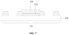
- FIG. 7 is a schematic sectional view of the substrate formed with the embankment and a pixel spacer in the method for making the organic light-emitting display panel according to one embodiment of the present disclosure.
- FIG. 8 is a schematic sectional view of the substrate formed with the pixel spacer and a buffer chamber in the method for making the organic light-emitting display panel according to one embodiment of the present disclosure.
- a reliability of a flexible display product is a main factor affecting the product yield.
- a reliability test when a ball having a weight of 32.65 g and a diameter of 20 mm is dropped from a height of 2 cm to 62.5 cm to strike a screen of a known flexible display product, a display defect, such as a black spot, a bright spot, and/or a color spot, occurs immediately on the area struck by the ball, revealing that the reliability of the known flexible display product does not satisfy the requirements of the practical application.
- the pixel spacer has an important role in achieving an impact resistance of the organic light-emitting display panel.
- the present disclosure provides an organic light-emitting display panel and a display device capable of avoiding the display defects and failure when struck by a heavy object.
- the organic light-emitting display panel of the present disclosure includes an active region and a pixel spacer located within the active region.
- the pixel spacer defines a buffer chamber.
- the organic light-emitting display panel can be an organic light-emitting diodes (OLED) display panel and so on.
- the organic light-emitting display panel can be a flexible display panel.
- the present disclosure if a region of the organic light-emitting display panel provided with the buffer chamber is struck by a heavy object, a route along which the stress is transferred downward is cut off by the buffer chamber, so that the stress would tend to be dissipated in other directions, thereby avoiding the damage of a functional layer located under the pixel spacer caused by the stress concentration and avoiding the display defects and failure. Furthermore, the reliability and the bending strength of the organic light-emitting display panel can be enhanced.
- an organic light-emitting display panel 100 provided in an embodiment of the present disclosure includes an active region 110 and a pixel spacer 120 located within the active region 110 .
- the pixel spacer 120 defines a buffer chamber 122 .
- the active region 110 refers to a region, in addition to a frame, of the organic light-emitting display panel 100 configured for displaying images.
- the organic light-emitting display panel 100 can also include a frame region (i.e. a non-active region, not shown) surrounding the active region 110 .
- the pixel spacer 120 can also be referred as a pixel-isolating pillar or a pixel-defining layer.
- the pixel spacer 120 surrounds a sub-pixel to define the location of the sub-pixel.
- the sub-pixel can be a red sub-pixel, a green sub-pixel, a blue sub-pixel, and so on.
- the buffer chamber 122 can be an enclosed chamber.
- the buffer chamber 122 can be defined inside the pixel spacer 120 .
- the buffer chamber 122 can also be a chamber with an open end.
- the buffer chamber 122 can be arranged on a surface of the pixel spacer 120 with a recess shape.
- the organic light-emitting display panel 100 can further include a base substrate 130 located at a side of the organic light-emitting.
- the buffer chamber 122 can be located adjacent to the base substrate 130 , as shown in FIG. 1 .
- the base substrate 130 is configured to support the functional layer formed thereon.
- the base substrate 130 can be a flexible base substrate made of a flexible material, such as polyimide (PI).
- the base substrate 130 itself can further include the functional layer, such as a buffer layer and a blocking layer.
- a region of the pixel spacer 120 located around the buffer chamber 122 can have a bridge shape.
- a force is applied to anywhere on the region of the bridge shaped pixel spacer 120 , a stress caused by the force can be dissipated in all directions rapidly, thereby effectively avoiding the damage of the function layer located under the pixel spacer 120 caused by the stress concentration and effectively avoiding the display defects and failure.
- the pixel spacer 120 can define a plurality of buffer chambers 122 .
- a ratio of an area of a projection of the plurality of buffer chambers 122 on the base substrate 130 to an area of a projection of the pixel spacer 120 on the base substrate 130 can be in a range from about 1:1 to about 1:50, such that the organic light-emitting display panel 100 can be fully protected by the buffer chambers 122 .
- the stress concentration can be substantially reduced, thereby avoiding the damage of the functional layer located under the pixel spacer 120 and avoiding the display defects and failure.
- the plurality of buffer chambers 122 can be uniformly distributed on the pixel spacer 120 . Uniform distribution means that distances between any two adjacent buffer chambers 122 can be substantially the same, although there might be a minor difference between the distances. Since the plurality of buffer chambers 122 are uniformly distributed on the pixel spacer 120 , the organic light-emitting display panel 100 can be fully protected by the buffer chambers 122 . When the organic light-emitting display panel 100 is struck by a heavy object, the stress concentration can be substantially reduced, thereby avoiding the damage of the functional layer located under the pixel spacer 120 and avoiding the display defects and failure.
- the pixel spacer 120 is provided with a plurality of buffer chambers 122 , and a ratio of an area of a projection of the plurality of buffer chambers 122 on the base substrate 130 to an area of a projection of the pixel spacer 120 on the base substrate 130 can be in a range from about 1:1 to about 1:50. As such, the stress concentration can be reduced to a greatest extent via the plurality of buffer chambers 122 .
- one, two, or more buffer chambers can be provided on the pixel spacer 120 between any two adjacent sub-pixels in the organic light-emitting display panel.
- an organic light-emitting display panel 200 provided in another embodiment of the present disclosure includes an active region 210 and a pixel spacer 220 located within an active region 210 .
- the pixel spacer 220 defines a buffer chamber 222 .
- the organic light-emitting display panel 200 includes a plurality of sub-pixels (such as a red sub-pixel and a green sub-pixel as shown in FIG. 3 ). Each of the plurality of sub-pixels can be surrounded by the pixel spacer 220 .
- a plurality of buffer chambers 222 for example, three buffer chambers 222 , can be defined by the pixel spacer 220 between any two adjacent sub-pixels, so that the stress can be dissipated in all directions via more paths so as to be dissipated relatively fast to effectively avoid the display defects and failure when the organic light-emitting display panel is struck by a heavy object.
- a number of the buffer chambers between two adjacent sub-pixels can be different from a number of the buffer chambers between another two adjacent sub-pixels.
- more buffer chambers can be defined at the location where larger stress would be caused by striking, and less buffer chambers can be defined at the location where smaller stress would be caused by striking.
- the dimensions of the plurality of buffer chambers can be the same or different in the organic light-emitting display panel provided in the present disclosure.
- lower ends of the plurality of buffer chambers 222 are coplanar with each other, and upper ends of the plurality of buffer chambers 222 are coplanar with each other.
- a method for forming the plurality of buffer chambers 222 is simple and easy to be implemented. It should be understood that the locations of the plurality of buffer chambers in the present disclosure is not limited to the embodiments as described above.
- an organic light-emitting display panel 300 provided in another embodiment of the present disclosure includes an active region 310 and a pixel spacer 320 located within the active region 310 .
- the pixel spacer 320 defines a plurality of buffer chambers 322 . At least two buffer chambers 322 can be arranged along a longitudinal direction.
- the longitudinal direction refers to a direction perpendicular to a displaying surface of an organic light-emitting display panel.
- the buffer chamber 322 located at a side of the pixel spacer 320 adjacent to the displaying surface can increase an area of the organic light-emitting display panel 300 in contact with the heavy object so as to decrease the intensity of pressure applied on the organic light-emitting display panel 300 .
- the buffer chamber 322 located at a side of the pixel spacer 320 away from the displaying surface can cut off the route along which the stress is transferred downward, so that the stress would tend to be dissipated in other directions, thereby avoiding the damage of the functional layer located under the buffer chamber 322 caused by the stress concentration. As such, the display defects and failure are avoided.
- the buffer chamber can have a trapezoidal cross-section perpendicular to the upper surface and/or the lower surface of the pixel spacer. It should be understood that the cross-section of the buffer chamber perpendicular to the upper surface and/or the lower surface of the pixel spacer can also has other shapes, such as an arched shape, a circular shape, an oval shape, a rectangular shape, a triangular shape, and so on, which is not limited herein.
- an organic light-emitting display panel 400 provided in another embodiment of the present disclosure includes an active region 410 and a pixel spacer 420 located within the active region 410 .
- the organic light-emitting display panel 400 further includes a cathode 440 located above the pixel spacer 420 and an anode 430 located under the pixel spacer 420 .
- the pixel spacer 420 is provided with a plurality of buffer chambers 422 .
- the buffer chamber 422 has an arched cross-section perpendicular to the upper surface and/or the lower surface of the pixel spacer 420 , as shown in FIG. 5 .
- the buffer chamber can be filled with a flexible filler (not shown) or an inert gas.
- the flexible filler or the inert gas acts as a buffer to reduce the stress squeezing the functional layer located under the buffer chamber when the region of the organic light-emitting display panel provided with the buffer chamber is subjected to a force.
- the inert gas can include helium gas, argon gas, or other inert gases.
- the flexible filler can be made of a silica gel or a liquid insulating material unable to react with a layer or film surrounding the flexible filler. Both of the silica gel and the liquid insulating material have a good buffering effect. It should be understood that the material of the flexible filler is not limited herein as long as the material has a good buffering effect.
- the organic light-emitting display panel provided in the present disclosure, when a region of the organic light-emitting display panel provided with the buffer chamber is struck by a heavy object, a route along which the stress is transferred downward would be cut off by the buffer chamber, so that the stress would tend to be dissipated in other directions, thereby avoiding the damage of a functional layer located under the pixel spacer caused by the stress concentration and avoiding the display defects and failure.
- a method for making the organic light-emitting display panel is further provided in the present disclosure.
- the method includes a step of forming the buffer chamber on the pixel spacer within the active region to obtain the organic light-emitting display panel.
- the step of forming the buffer chamber on the pixel spacer within the active region includes steps of:
- the substrate is configured to support the patterned embankment.
- the substrate can be the functional layer of the organic light-emitting display panel which is to be located under the subsequently formed pixel spacer, so that the buffer chamber formed in the subsequent step is arranged on the surface of the pixel spacer.
- the substrate can be a portion of the pixel spacer, the patterned embankment can be formed on the portion of the pixel spacer, and another portion of the pixel spacer can be formed on the patterned embankment, so that the buffer chamber formed in the subsequent step is located inside the pixel spacer.
- the substrate is the base substrate 130 .
- a patterned embankment 121 is formed on the base substrate 130 within the active region 110 .
- the embankment 121 is configured for forming the buffer chamber in the subsequent step.
- the region where the embankment 121 is located at is the region where the buffer chamber is to be located at.
- the subsequently formed buffer chamber has the same dimension as the embankment 121 .
- the embankment 121 can be made of an inorganic compound, such as silicon oxide, silicon nitride, and so on.
- the patterned embankment 121 can be prepared by means of wet etching, high selectivity dry etching, and as on.
- a continuous layer of pixel spacer precursor can be formed on the substrate formed with the patterned embankment 121 by a method such as coating. Then the continuous layer of pixel spacer precursor is patterned (for example, by etching) to form the pixel spacer 120 covered on the embankment 121 , as shown in FIG. 7 .
- the embankment 121 located under the pixel spacer 120 can be removed by etching method.
- a through hole can be formed on the pixel spacer 120 to expose the embankment 121 located under the pixel spacer 120 , then an etching solution can be in contact with the embankment 121 via the through hole to etch the embankment 121 until the embankment 121 is completely removed, so as to form the buffer chamber 122 , as shown in FIG. 8 .
- Other layers, such as a light-emitting layer and a cathode, if required, can be formed on the pixel spacer 120 to form the organic light-emitting display panel as shown in FIG. 1 .
- the flexible filler if required, can also be filled into the buffer chamber 122 via the through hole.
- the embankment can be made of a material which can be decomposed under light (any kind of light, such as ultraviolet light). After the pixel spacer 120 is formed, the embankment can be exposed to the light to be removed, thereby forming the buffer chamber.
- the buffer chamber 122 is defined by the lower surface of the pixel spacer 120 and is located adjacent to the base substrate 130 .
- the location of the buffer chamber 122 in the organic light-emitting display panel of the present disclosure is not limited thereto.
- the buffer chamber 122 can also be defined by the upper surface of the pixel spacer 120 , in this case, a pixel spacer precursor can be formed firstly, and then a buffer chamber can be formed on the upper surface of the pixel spacer 120 by imprinting or etching the pixel spacer precursor.
- a display device is further provided in the present disclosure.
- the display device includes the organic light-emitting display panel provided in any one of the above described embodiments.
- the display device By using the display device provided in the present disclosure, when a region of the organic light-emitting display panel provided with the buffer chamber is struck by a heavy object, a route along which the stress is transferred downward would be cut off by the buffer chamber, so that the stress would tend to be dissipated in other directions, thereby avoiding the damage of a functional layer located under the pixel spacer caused by the stress concentration and avoiding the display defects and failure.
Landscapes
- Engineering & Computer Science (AREA)
- Microelectronics & Electronic Packaging (AREA)
- Physics & Mathematics (AREA)
- Optics & Photonics (AREA)
- Manufacturing & Machinery (AREA)
- Geometry (AREA)
- Electroluminescent Light Sources (AREA)
Abstract
Description
Claims (17)
Applications Claiming Priority (3)
| Application Number | Priority Date | Filing Date | Title |
|---|---|---|---|
| CN201810813127.3 | 2018-07-23 | ||
| CN201810813127.3A CN108962954B (en) | 2018-07-23 | 2018-07-23 | Organic light-emitting display screen, manufacturing method thereof and display device |
| PCT/CN2019/084861 WO2020019803A1 (en) | 2018-07-23 | 2019-04-28 | Organic light-emitting display screen and manufacturing method therefor, and display device |
Related Parent Applications (1)
| Application Number | Title | Priority Date | Filing Date |
|---|---|---|---|
| PCT/CN2019/084861 Continuation WO2020019803A1 (en) | 2018-07-23 | 2019-04-28 | Organic light-emitting display screen and manufacturing method therefor, and display device |
Publications (2)
| Publication Number | Publication Date |
|---|---|
| US20200144531A1 US20200144531A1 (en) | 2020-05-07 |
| US11217768B2 true US11217768B2 (en) | 2022-01-04 |
Family
ID=64464434
Family Applications (1)
| Application Number | Title | Priority Date | Filing Date |
|---|---|---|---|
| US16/734,429 Active US11217768B2 (en) | 2018-07-23 | 2020-01-06 | Organic light-emitting display panels, methods for making the same, and display devices |
Country Status (3)
| Country | Link |
|---|---|
| US (1) | US11217768B2 (en) |
| CN (1) | CN108962954B (en) |
| WO (1) | WO2020019803A1 (en) |
Families Citing this family (5)
| Publication number | Priority date | Publication date | Assignee | Title |
|---|---|---|---|---|
| CN108962954B (en) | 2018-07-23 | 2021-01-26 | 云谷(固安)科技有限公司 | Organic light-emitting display screen, manufacturing method thereof and display device |
| CN109755287B (en) * | 2019-02-25 | 2021-12-28 | 武汉华星光电半导体显示技术有限公司 | Flexible OLED device and preparation method thereof |
| CN111312790B (en) * | 2020-02-28 | 2023-08-18 | 上海天马微电子有限公司 | Display panel, manufacturing method and flexible display device |
| WO2023178591A1 (en) * | 2022-03-24 | 2023-09-28 | 京东方科技集团股份有限公司 | Display substrate and preparation method therefor, and display device |
| CN115867079A (en) * | 2022-12-27 | 2023-03-28 | 上海天马微电子有限公司 | Display panel and display device |
Citations (15)
| Publication number | Priority date | Publication date | Assignee | Title |
|---|---|---|---|---|
| US20070228937A1 (en) | 2004-12-15 | 2007-10-04 | Muneharu Akiyoshi | Display device and method of manufacturing the display device |
| US20090058294A1 (en) * | 2007-09-05 | 2009-03-05 | Young-Cheol Joo | Light emitting display device and method for fabricating the same |
| US20130248867A1 (en) * | 2012-03-23 | 2013-09-26 | Mu-gyeom Kim | Flexible display apparatus and method of manufacturing the same |
| US8711469B2 (en) * | 2011-02-17 | 2014-04-29 | Sony Corporation | Electrophoretic element and display device |
| US20150144917A1 (en) * | 2013-11-22 | 2015-05-28 | Samsung Display Co., Ltd. | Organic light emitting display device and method of manufacturing the same |
| US20160254476A1 (en) | 2015-02-26 | 2016-09-01 | Samsung Display Co., Ltd. | Organic light emitting diode display |
| CN106876331A (en) * | 2017-03-03 | 2017-06-20 | 武汉华星光电技术有限公司 | OLED display panel and preparation method thereof, display device |
| CN106920826A (en) | 2017-02-27 | 2017-07-04 | 上海天马微电子有限公司 | Flexible display panel, manufacturing method thereof and display device |
| US20170207416A1 (en) * | 2016-01-15 | 2017-07-20 | Samsung Display Co., Ltd. | Organic light-emitting display apparatus and method of manufacturing the same |
| CN107068721A (en) | 2017-04-20 | 2017-08-18 | 京东方科技集团股份有限公司 | Pixel unit, manufacturing method thereof, and display device |
| CN206480628U (en) | 2017-02-28 | 2017-09-08 | 武汉天马微电子有限公司 | An organic light emitting display panel |
| US20180012944A1 (en) | 2016-07-08 | 2018-01-11 | Japan Display Inc. | Display device |
| CN107611162A (en) | 2017-09-13 | 2018-01-19 | 武汉华星光电半导体显示技术有限公司 | Flexible OLED display panel and preparation method thereof |
| CN206976349U (en) | 2017-06-30 | 2018-02-06 | 昆山国显光电有限公司 | Oled display panel |
| CN108962954A (en) | 2018-07-23 | 2018-12-07 | 云谷(固安)科技有限公司 | Organic light emitting display and preparation method thereof and display device |
-
2018
- 2018-07-23 CN CN201810813127.3A patent/CN108962954B/en active Active
-
2019
- 2019-04-28 WO PCT/CN2019/084861 patent/WO2020019803A1/en not_active Ceased
-
2020
- 2020-01-06 US US16/734,429 patent/US11217768B2/en active Active
Patent Citations (17)
| Publication number | Priority date | Publication date | Assignee | Title |
|---|---|---|---|---|
| CN101076842A (en) | 2004-12-15 | 2007-11-21 | 东芝松下显示技术有限公司 | Display device and display device manufacturing method |
| US20070228937A1 (en) | 2004-12-15 | 2007-10-04 | Muneharu Akiyoshi | Display device and method of manufacturing the display device |
| US20090058294A1 (en) * | 2007-09-05 | 2009-03-05 | Young-Cheol Joo | Light emitting display device and method for fabricating the same |
| US8711469B2 (en) * | 2011-02-17 | 2014-04-29 | Sony Corporation | Electrophoretic element and display device |
| US20130248867A1 (en) * | 2012-03-23 | 2013-09-26 | Mu-gyeom Kim | Flexible display apparatus and method of manufacturing the same |
| US20150144917A1 (en) * | 2013-11-22 | 2015-05-28 | Samsung Display Co., Ltd. | Organic light emitting display device and method of manufacturing the same |
| US20160254476A1 (en) | 2015-02-26 | 2016-09-01 | Samsung Display Co., Ltd. | Organic light emitting diode display |
| US20170207416A1 (en) * | 2016-01-15 | 2017-07-20 | Samsung Display Co., Ltd. | Organic light-emitting display apparatus and method of manufacturing the same |
| US20180012944A1 (en) | 2016-07-08 | 2018-01-11 | Japan Display Inc. | Display device |
| CN106920826A (en) | 2017-02-27 | 2017-07-04 | 上海天马微电子有限公司 | Flexible display panel, manufacturing method thereof and display device |
| CN206480628U (en) | 2017-02-28 | 2017-09-08 | 武汉天马微电子有限公司 | An organic light emitting display panel |
| CN106876331A (en) * | 2017-03-03 | 2017-06-20 | 武汉华星光电技术有限公司 | OLED display panel and preparation method thereof, display device |
| US20180301521A1 (en) | 2017-03-03 | 2018-10-18 | Wuhan China Star Optoelectronics Technology Co., Ltd. | Oled display panel and manufacturing method and display device thereof |
| CN107068721A (en) | 2017-04-20 | 2017-08-18 | 京东方科技集团股份有限公司 | Pixel unit, manufacturing method thereof, and display device |
| CN206976349U (en) | 2017-06-30 | 2018-02-06 | 昆山国显光电有限公司 | Oled display panel |
| CN107611162A (en) | 2017-09-13 | 2018-01-19 | 武汉华星光电半导体显示技术有限公司 | Flexible OLED display panel and preparation method thereof |
| CN108962954A (en) | 2018-07-23 | 2018-12-07 | 云谷(固安)科技有限公司 | Organic light emitting display and preparation method thereof and display device |
Non-Patent Citations (2)
| Title |
|---|
| International Search Report of International Patent Application No. PCT/CN2019/084861. |
| Office Action of Chinese Patent Application No. 201810813127.3. |
Also Published As
| Publication number | Publication date |
|---|---|
| US20200144531A1 (en) | 2020-05-07 |
| CN108962954B (en) | 2021-01-26 |
| WO2020019803A1 (en) | 2020-01-30 |
| CN108962954A (en) | 2018-12-07 |
Similar Documents
| Publication | Publication Date | Title |
|---|---|---|
| US11217768B2 (en) | Organic light-emitting display panels, methods for making the same, and display devices | |
| US10483338B2 (en) | Organic light-emitting display panel, manufacturing method thereof, and organic light-emitting display device | |
| CN111682120B (en) | Display panel, manufacturing method thereof, and display device | |
| US8087965B2 (en) | Organic electro-luminescence display device and method for fabricating the same | |
| US9722005B2 (en) | Light-emitting device, array substrate, display device and manufacturing method of light-emitting device | |
| KR101814775B1 (en) | Fabricating Method Of Organic Light Emitting Diode Display | |
| US9373814B2 (en) | Organic light-emitting diode (OLED) display panel, pixel define layer (PDL) and preparation method thereof | |
| US12501767B2 (en) | Display panel with isolation spacer including groove-shaped structure, fabrication method therefor, and display apparatus | |
| US9960218B2 (en) | Organic light-emitting display substrate, manufacturing method therefor, and organic light-emitting display device | |
| JP4703873B2 (en) | OLED display device | |
| US11239282B2 (en) | Pixel structure and fabrication method thereof, display substrate and display apparatus | |
| CN110277508B (en) | Organic light emitting diode display panel and manufacturing method thereof | |
| WO2021254033A1 (en) | Flexible display substrate and manufacturing method therefor, and display device | |
| KR102303734B1 (en) | Array substrate and its manufacturing method, display panel and its manufacturing method | |
| WO2020164528A1 (en) | Display substrate and method for preparing same, and display apparatus | |
| US20260007041A1 (en) | Display panel and manufacturing method therefor, and display apparatus | |
| KR20130007005A (en) | Mask for forming patterns and organic light emitting display device | |
| CN100421252C (en) | Organic electroluminescent display device and method of fabricating the same | |
| US20240244927A1 (en) | Display panel and manufacturing method thereof | |
| US11011591B2 (en) | Organic light emitting diode display panel and method for fabricating same | |
| EP1422976B1 (en) | Method for manufacturing organic el device and organic el device | |
| CN118139473A (en) | Display panel, preparation method thereof and display device | |
| CN110610974A (en) | Display panel, manufacturing method thereof and display terminal | |
| KR101595471B1 (en) | Organic electroluminescent device and manufacturing method thereof | |
| KR101202547B1 (en) | Organic Electroluminescent Device and method for fabricating thereof |
Legal Events
| Date | Code | Title | Description |
|---|---|---|---|
| AS | Assignment |
Owner name: YUNGU (GU'AN) TECHNOLOGY CO., LTD., CHINA Free format text: ASSIGNMENT OF ASSIGNORS INTEREST;ASSIGNORS:LIU, RUSHENG;YUAN, BO;HUANG, GENMAO;AND OTHERS;REEL/FRAME:051417/0679 Effective date: 20190709 |
|
| FEPP | Fee payment procedure |
Free format text: ENTITY STATUS SET TO UNDISCOUNTED (ORIGINAL EVENT CODE: BIG.); ENTITY STATUS OF PATENT OWNER: LARGE ENTITY |
|
| STPP | Information on status: patent application and granting procedure in general |
Free format text: DOCKETED NEW CASE - READY FOR EXAMINATION |
|
| STPP | Information on status: patent application and granting procedure in general |
Free format text: RESPONSE TO NON-FINAL OFFICE ACTION ENTERED AND FORWARDED TO EXAMINER |
|
| STPP | Information on status: patent application and granting procedure in general |
Free format text: NON FINAL ACTION MAILED |
|
| STPP | Information on status: patent application and granting procedure in general |
Free format text: RESPONSE TO NON-FINAL OFFICE ACTION ENTERED AND FORWARDED TO EXAMINER |
|
| STPP | Information on status: patent application and granting procedure in general |
Free format text: FINAL REJECTION MAILED |
|
| STPP | Information on status: patent application and granting procedure in general |
Free format text: ADVISORY ACTION MAILED |
|
| STPP | Information on status: patent application and granting procedure in general |
Free format text: DOCKETED NEW CASE - READY FOR EXAMINATION |
|
| STPP | Information on status: patent application and granting procedure in general |
Free format text: NOTICE OF ALLOWANCE MAILED -- APPLICATION RECEIVED IN OFFICE OF PUBLICATIONS |
|
| STPP | Information on status: patent application and granting procedure in general |
Free format text: PUBLICATIONS -- ISSUE FEE PAYMENT RECEIVED |
|
| STPP | Information on status: patent application and granting procedure in general |
Free format text: PUBLICATIONS -- ISSUE FEE PAYMENT VERIFIED |
|
| STCF | Information on status: patent grant |
Free format text: PATENTED CASE |
|
| MAFP | Maintenance fee payment |
Free format text: PAYMENT OF MAINTENANCE FEE, 4TH YEAR, LARGE ENTITY (ORIGINAL EVENT CODE: M1551); ENTITY STATUS OF PATENT OWNER: LARGE ENTITY Year of fee payment: 4 |
|
| AS | Assignment |
Owner name: SUZHOU GOVISIONOX INNOVATION TECHNOLOGY CO., LTD., CHINA Free format text: ASSIGNMENT OF ASSIGNORS INTEREST;ASSIGNOR:YUNGU (GU'AN) TECHNOLOGY CO., LTD.;REEL/FRAME:073414/0132 Effective date: 20260107 |