US11216593B2 - Data protection circuit of chip, chip, and electronic device - Google Patents
Data protection circuit of chip, chip, and electronic device Download PDFInfo
- Publication number
- US11216593B2 US11216593B2 US16/411,230 US201916411230A US11216593B2 US 11216593 B2 US11216593 B2 US 11216593B2 US 201916411230 A US201916411230 A US 201916411230A US 11216593 B2 US11216593 B2 US 11216593B2
- Authority
- US
- United States
- Prior art keywords
- descrambling
- circuit
- signal
- processing
- alarm
- Prior art date
- Legal status (The legal status is an assumption and is not a legal conclusion. Google has not performed a legal analysis and makes no representation as to the accuracy of the status listed.)
- Active
Links
Images


Classifications
-
- G—PHYSICS
- G06—COMPUTING; CALCULATING OR COUNTING
- G06F—ELECTRIC DIGITAL DATA PROCESSING
- G06F21/00—Security arrangements for protecting computers, components thereof, programs or data against unauthorised activity
- G06F21/70—Protecting specific internal or peripheral components, in which the protection of a component leads to protection of the entire computer
- G06F21/71—Protecting specific internal or peripheral components, in which the protection of a component leads to protection of the entire computer to assure secure computing or processing of information
- G06F21/72—Protecting specific internal or peripheral components, in which the protection of a component leads to protection of the entire computer to assure secure computing or processing of information in cryptographic circuits
-
- G—PHYSICS
- G06—COMPUTING; CALCULATING OR COUNTING
- G06F—ELECTRIC DIGITAL DATA PROCESSING
- G06F21/00—Security arrangements for protecting computers, components thereof, programs or data against unauthorised activity
- G06F21/60—Protecting data
- G06F21/602—Providing cryptographic facilities or services
-
- G—PHYSICS
- G06—COMPUTING; CALCULATING OR COUNTING
- G06F—ELECTRIC DIGITAL DATA PROCESSING
- G06F11/00—Error detection; Error correction; Monitoring
- G06F11/07—Responding to the occurrence of a fault, e.g. fault tolerance
- G06F11/08—Error detection or correction by redundancy in data representation, e.g. by using checking codes
- G06F11/10—Adding special bits or symbols to the coded information, e.g. parity check, casting out 9's or 11's
- G06F11/1004—Adding special bits or symbols to the coded information, e.g. parity check, casting out 9's or 11's to protect a block of data words, e.g. CRC or checksum
-
- G—PHYSICS
- G06—COMPUTING; CALCULATING OR COUNTING
- G06F—ELECTRIC DIGITAL DATA PROCESSING
- G06F11/00—Error detection; Error correction; Monitoring
- G06F11/07—Responding to the occurrence of a fault, e.g. fault tolerance
- G06F11/08—Error detection or correction by redundancy in data representation, e.g. by using checking codes
- G06F11/10—Adding special bits or symbols to the coded information, e.g. parity check, casting out 9's or 11's
- G06F11/1008—Adding special bits or symbols to the coded information, e.g. parity check, casting out 9's or 11's in individual solid state devices
- G06F11/1012—Adding special bits or symbols to the coded information, e.g. parity check, casting out 9's or 11's in individual solid state devices using codes or arrangements adapted for a specific type of error
- G06F11/1032—Simple parity
-
- G—PHYSICS
- G06—COMPUTING; CALCULATING OR COUNTING
- G06F—ELECTRIC DIGITAL DATA PROCESSING
- G06F21/00—Security arrangements for protecting computers, components thereof, programs or data against unauthorised activity
- G06F21/60—Protecting data
-
- G—PHYSICS
- G06—COMPUTING; CALCULATING OR COUNTING
- G06F—ELECTRIC DIGITAL DATA PROCESSING
- G06F21/00—Security arrangements for protecting computers, components thereof, programs or data against unauthorised activity
- G06F21/70—Protecting specific internal or peripheral components, in which the protection of a component leads to protection of the entire computer
- G06F21/71—Protecting specific internal or peripheral components, in which the protection of a component leads to protection of the entire computer to assure secure computing or processing of information
- G06F21/75—Protecting specific internal or peripheral components, in which the protection of a component leads to protection of the entire computer to assure secure computing or processing of information by inhibiting the analysis of circuitry or operation
-
- G—PHYSICS
- G06—COMPUTING; CALCULATING OR COUNTING
- G06F—ELECTRIC DIGITAL DATA PROCESSING
- G06F21/00—Security arrangements for protecting computers, components thereof, programs or data against unauthorised activity
- G06F21/70—Protecting specific internal or peripheral components, in which the protection of a component leads to protection of the entire computer
- G06F21/78—Protecting specific internal or peripheral components, in which the protection of a component leads to protection of the entire computer to assure secure storage of data
Definitions
- This application relates to chip technologies, and in particular, to a data protection circuit of a chip, a chip, and an electronic device.
- a chip is an important component of a mobile terminal, a computer, or another electronic device, and is responsible for functions such as calculation and storage.
- the chip generates data and stores the data in an operating state, and a part or all of the data requires high confidentiality. For example, data that is generated and stored by a security chip in an operating state. Therefore, it is particularly important to prevent data of a chip from being stolen.
- a chip in other approaches, includes an operation module and a clock reset module, and the operation module is connected to the clock reset module.
- the operation module When subjected to an external attack, the operation module generates an alarm signal of an active level, and the clock reset module generates a reset request signal of an active level according to the alarm signal, and triggers resetting of the chip such that the chip is restored to an initialization state in order to prevent data of the chip from being stolen.
- This application provides a data protection circuit of a chip, a chip, and an electronic device, to resolve a problem that chip security is not high.
- An aspect of this application provides a data protection circuit of a chip, and the circuit includes an operation module, an alarm management module, and a reset module, the alarm management module includes a processing unit and a reset request unit, and the processing unit is connected to the operation module.
- the operation module After generating a first alarm signal, the operation module performs bit width expansion and scrambling processing on the first alarm signal to obtain a second alarm signal, and the operation module sends a second alarm signal to the processing unit.
- the processing unit performs descrambling processing on the second alarm signal to obtain a descrambling result, and outputs the descrambling result to the reset request unit.
- the reset request unit generates a reset request signal according to the descrambling result, and sends the reset request signal to the reset module.
- the reset module determines, according to the reset request signal, whether to reset some or all operation modules of the chip.
- the first alarm signal When the operation module detects an attack signal, the first alarm signal is an active level, or when the operation module detects no attack signal, the first alarm signal is an inactive level, when descrambling performed by the processing unit succeeds, if the first alarm signal is an active level, the descrambling result is an active level, or if the first alarm signal is an inactive level, the descrambling result is an inactive level, or when descrambling performed by the processing unit fails, the descrambling result is an active level, and when the descrambling result is an active level, the reset request signal is an active level, or when the descrambling result is an inactive level, the reset request signal is an inactive level.
- the data protection circuit of the chip performs bit width expansion and scrambling processing on the first alarm signal using the operation module to obtain the second alarm signal, and outputs the second alarm signal to the processing unit.
- the processing unit performs descrambling processing after receiving the second alarm signal to obtain the descrambling result.
- the descrambling fails, and the descrambling result is an active level.
- the processing unit outputs the descrambling result to the reset request unit, and the reset request unit generates the reset request signal according to the descrambling result. Therefore, even if the second alarm signal is attacked, the reset request unit can output the reset request signal, to protect data of the operation module from being stolen in order to improve chip security.
- the processing unit includes a first descrambling processing subunit, a first delay processing subunit, a second delay processing subunit, a second descrambling processing subunit, a comparator, and a first OR gate unit.
- An input end of the first descrambling processing subunit is connected to an output end of the operation module, an output end of the first descrambling processing subunit is connected to an input end of the first delay processing subunit, and an output end of the first delay processing subunit is connected to a first input end of the comparator.
- An input end of the second delay processing subunit is connected to the output end of the operation module, an output end of the second delay processing subunit is connected to an input end of the second descrambling processing subunit, and an output end of the second descrambling processing subunit is connected to a second input end of the comparator.
- the output end of the second descrambling processing subunit is further connected to a first input end of the first OR gate unit, an output end of the comparator is connected to a second input end of the first OR gate unit, and an output end of the first OR gate unit is configured to output the descrambling result.
- Both the first descrambling processing subunit and the second descrambling processing subunit are configured to perform descrambling processing.
- Both the first delay processing subunit and the second delay processing subunit are configured to perform delay processing.
- the output end of the first descrambling processing subunit When descrambling performed by the first descrambling processing subunit succeeds, if the first alarm signal is an active level, the output end of the first descrambling processing subunit outputs an active level, or if the first alarm signal is an inactive level, the output end of the first descrambling processing subunit outputs an inactive level, or when descrambling performed by the first descrambling processing subunit fails, the output end of the first descrambling processing subunit outputs an active level.
- the output end of the second descrambling processing subunit When descrambling performed by the second descrambling processing subunit succeeds, if the first alarm signal is an active level, the output end of the second descrambling processing subunit outputs an active level, or if the first alarm signal is an inactive level, the output end of the second descrambling processing subunit outputs an inactive level, or when descrambling performed by the second descrambling processing subunit fails, the output end of the second descrambling processing subunit outputs an active level.
- the processing unit includes a first descrambling processing subunit, a first delay processing subunit, a second delay processing subunit, a second descrambling processing subunit, a comparator, and a first OR gate unit.
- An input end of the first descrambling processing subunit is connected to an output end of the operation module, an output end of the first descrambling processing subunit is connected to an input end of the first delay processing subunit, and an output end of the first delay processing subunit is connected to a first input end of the comparator.
- An input end of the second delay processing subunit is connected to the output end of the operation module, an output end of the second delay processing subunit is connected to an input end of the second descrambling processing subunit, and an output end of the second descrambling processing subunit is connected to a second input end of the comparator.
- the output end of the first delay processing subunit is further connected to a first input end of the first OR gate unit, an output end of the comparator is connected to a second input end of the first OR gate unit, and an output end of the first OR gate unit is configured to output the descrambling result.
- Both the first descrambling processing subunit and the second descrambling processing subunit are configured to perform descrambling processing.
- Both the first delay processing subunit and the second delay processing subunit are configured to perform delay processing.
- the output end of the first descrambling processing subunit When descrambling performed by the first descrambling processing subunit succeeds, if the first alarm signal is an active level, the output end of the first descrambling processing subunit outputs an active level, or if the first alarm signal is an inactive level, the output end of the first descrambling processing subunit outputs an inactive level, or when descrambling performed by the first descrambling processing subunit fails, the output end of the first descrambling processing subunit outputs an active level.
- the output end of the second descrambling processing subunit When descrambling performed by the second descrambling processing subunit succeeds, if the first alarm signal is an active level, the output end of the second descrambling processing subunit outputs an active level, or if the first alarm signal is an inactive level, the output end of the second descrambling processing subunit outputs an inactive level, or when descrambling performed by the second descrambling processing subunit fails, the output end of the second descrambling processing subunit outputs an active level.
- the processing unit includes a descrambling module.
- An input end of the descrambling module is connected to an output end of the operation module, an output end of the descrambling module is connected to an input end of the reset request unit, and the descrambling module is configured to receive the second alarm signal, and perform descrambling processing on the second alarm signal to obtain the descrambling result.
- the descrambling result is an active level, or if the first alarm signal is an inactive level, the descrambling result is an inactive level, or when descrambling performed by the descrambling module fails, the descrambling result is an active level.
- the reset request unit is a first AND gate unit, a first input end of the first AND gate unit is connected to the output end of the first OR gate unit, a second input end of the first AND gate unit is configured to input an alarm enable signal, and an output end of the first AND gate unit is configured to output the reset request signal.
- the first OR gate unit is disposed, and when an active level that is output by the output end of the comparator is attacked, or when an active level that is input by the second descrambling processing subunit to the second input end of the first OR gate unit is attacked, the output end of the first OR gate unit outputs an active level. Therefore, when the first alarm signal is a high level, regardless of whether the second alarm signal is attacked, the descrambling result that is output by the first OR gate unit is an active level. Therefore, the first OR gate unit can successfully transmit an alarm signal to the reset request unit. When the descrambling result received by the reset request unit is an active level, the generated reset request signal is an active level. When the received reset request signal is an active level, the reset module performs reset processing on the some or all operation modules of the chip. Therefore, data of the operation module is protected from being stolen, and chip security is improved.
- the alarm enable signal is controlled by a register, and the register is configured by software.
- a second alarm enable signal may be an active level by modifying the register.
- the alarm enable signal is controlled by a one-time programmable device.
- the circuit further includes a second OR gate unit, where an output end of the second OR gate unit is configured to output the alarm enable signal, a first input end of the second OR gate unit is configured to input a first alarm enable signal, a second input end of the second OR gate unit is configured to input a second alarm enable signal, the first alarm enable signal is controlled by a one-time programmable device, the second alarm enable signal is controlled by a register, and the register is configured by software.
- the reset request unit is implemented using the first AND gate unit.
- the alarm enable signal is used as input of the first AND gate unit.
- the reset request signal that is output by the output end of the first AND gate unit is an active level.
- the alarm enable signal may be set to an inactive signal in order to ensure normal use of a chip in the testing scenario or another scenario.
- the circuit further includes a second AND gate unit, where a first input end of the second AND gate unit is configured to input an alarm interruption enable signal, a second input end of the second AND gate unit is connected to the output end of the first OR gate unit, an output end of the second AND gate unit is configured to input an interruption signal to a central processing unit (CPU), and the interruption signal is configured to trigger the CPU to execute an alarm processing program.
- a second AND gate unit where a first input end of the second AND gate unit is configured to input an alarm interruption enable signal, a second input end of the second AND gate unit is connected to the output end of the first OR gate unit, an output end of the second AND gate unit is configured to input an interruption signal to a central processing unit (CPU), and the interruption signal is configured to trigger the CPU to execute an alarm processing program.
- CPU central processing unit
- a scrambling processing manner includes any one of cyclic redundancy check (CRC), parity check, or encryption.
- CRC cyclic redundancy check
- parity check or encryption.
- the one-time programmable device is an electrical fuse (Efuse).
- the active level is a high level
- the inactive level is a low level
- Another aspect of this application provides a chip, including the data protection circuit according to any one of the foregoing aspect or possible designs in the foregoing aspect.
- Still another aspect of this application provides an electronic device, including the chip according to the foregoing aspect.
- FIG. 1 is a schematic structural diagram of a data protection circuit of a chip according to Embodiment 1 of this application;
- FIG. 2 is a schematic structural diagram of a data protection circuit of a chip according to Embodiment 2 of this application;
- FIG. 3 is a schematic structural diagram of a data protection circuit of a chip according to Embodiment 3 of this application;
- FIG. 4 is a schematic structural diagram of a data protection circuit of a chip according to Embodiment 4 of this application;
- FIG. 5 is a schematic structural diagram of a data protection circuit of a chip according to Embodiment 5 of this application;
- FIG. 6A and FIG. 6B are schematic structural diagrams of a data protection circuit of a chip according to Embodiment 6 of this application.
- FIG. 7A and FIG. 7B are schematic structural diagrams of a data protection circuit of a chip according to Embodiment 7 of this application.
- An active level described in the following embodiments may be represented by a high level, and correspondingly, an inactive level is represented by a low level.
- An active level may also be represented by a low level, and correspondingly, an inactive level is represented by a high level. This application imposes no limitation herein.
- a chip includes multiple operation modules, and the following embodiments are described using an example in which one operation module is attacked.
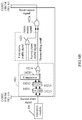
- FIG. 1 is a schematic structural diagram of a data protection circuit of a chip according to Embodiment 1 of this application.
- the data protection circuit includes an operation module 101 , an alarm management module 102 , and a reset module 103 .
- the alarm management module 102 includes a processing unit 1021 and a reset request unit 1022 .
- the operation module 101 is connected to the processing unit 1021 of the alarm management module 102
- the processing unit 1021 is connected to the reset request unit 1022
- the reset request unit 1022 is connected to the reset module 103 .
- the operation module generates a first alarm signal according to whether an attack signal is detected.
- the operation module detects the attack signal, and the generated first alarm signal is an active level.
- the operation module detects no attack signal, the generated first alarm signal is an inactive level.
- the operation module performs bit width expansion on the first alarm signal, that is, a single-bit (bit) signal is expanded to a multi-bit (such as, 4 bits, 16 bits, or 32 bits) signal, and performs scrambling processing on the multi-bit signal to obtain a second alarm signal.
- a scrambling processing manner includes but is not limited to a CRC manner, a parity check manner, and an encryption manner.
- the operation module outputs the second alarm signal to the processing unit, and the processing unit performs descrambling processing after receiving the second alarm signal to obtain a descrambling result. Further, when descrambling performed by the processing unit succeeds, the descrambling result is consistent with the first alarm signal.
- the first alarm signal is an active level
- the descrambling result is an active level
- the first alarm signal is an inactive level
- the descrambling result is an inactive level.
- the descrambling result is an active level, that is, that the descrambling fails indicates that the second alarm signal is attacked in a transmission process, and the descrambling result is an active level regardless of whether the first alarm signal is an active level or an inactive level.
- the processing unit obtains the descrambling result, and outputs the descrambling result to the reset request unit.
- the reset request unit generates a reset request signal according to the descrambling result, and sends the reset request signal to the reset module. Further, the reset request signal generated by the reset request unit is consistent with the descrambling result, that is, when the descrambling result is an active level, the reset request signal is an active level, or when the descrambling result is an inactive level, the reset request signal is an inactive level.
- the reset module determines, according to the reset request signal, whether to reset some or all operation modules of the chip. When the reset request signal is an active level, the reset module resets the some or all operation modules, or when the reset request signal is an inactive level, the reset module does not perform reset.
- the operation module when the operation module is attacked, the first alarm signal generated by the operation module is an active level, and the operation module sends the second alarm signal to the processing unit. If descrambling succeeds, the descrambling result is consistent with the first alarm signal, that is, the descrambling result is an active level. If descrambling fails, it indicates that the second alarm signal is attacked, and the descrambling result is an active level. Therefore, when the first alarm signal is an active level, regardless of whether the first alarm signal is attacked, the descrambling result that is output by the processing unit to the reset request unit is an active level such that the processing unit can successfully transmit an alarm signal to the reset request unit.
- the generated reset request signal is an active level.
- the reset module performs reset processing on the some or all operation modules of the chip. Therefore, data of the operation module is protected from being stolen, and chip security is improved.
- the operation module performs bit width expansion and scrambling processing on the first alarm signal to obtain the second alarm signal, and outputs the second alarm signal to the processing unit.
- the processing unit performs descrambling processing after receiving the second alarm signal to obtain the descrambling result.
- the descrambling fails, and the descrambling result is an active level.
- the processing unit outputs the descrambling result to the reset request unit, and the reset request unit generates the reset request signal according to the descrambling result. Therefore, even if the second alarm signal is attacked, the reset request unit can output the reset request signal to protect data of the operation module from being stolen in order to improve chip security.
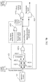
- FIG. 2 is a schematic structural diagram of a data protection circuit of a chip according to Embodiment 2 of this application.
- Embodiment 2 describes a possible implementation of the processing unit 1021 based on Embodiment 1.
- the processing unit 1021 includes a first descrambling processing subunit 10211 , a first delay processing subunit 10212 , a second delay processing subunit 10213 , a second descrambling processing subunit 10214 , a comparator 10215 , and a first OR gate unit 10216 .
- the first descrambling processing subunit and the second descrambling processing subunit in the following embodiments are represented by “S”, and the first delay processing subunit and the second delay processing subunit are represented by “D”.
- the processing unit includes two signal processing paths, in one path, descrambling processing is performed before delay processing, and in the other path, delay processing is performed before descrambling processing. That is, in the two signal processing paths, a time point to perform descrambling processing is different from a time point to perform delay processing. Delay processing is performed at different time points such that signals transmitted on the two signal processing paths are different at a same time point in a time domain. Therefore, a result in which signals on the two signal processing paths are the same after being attacked at the same time point is avoided such that when signals on the two signal processing paths are attacked simultaneously, an output result of the comparator is an active level. Details are shown in the following.
- One signal processing path includes the first descrambling processing subunit 10211 and the first delay processing subunit 10212 .
- An input end of the first descrambling processing subunit 10211 is connected to an output end of the operation module 101 .
- An output end of the first descrambling processing subunit 10211 is connected to an input end of the first delay processing subunit 10212 .
- An output end of the first delay processing subunit 10212 is connected to a first input end of the comparator 10215 .
- the other signal processing path includes the second delay processing subunit 10213 and the second descrambling processing subunit 10214 .
- An input end of the second delay processing subunit 10213 is connected to the output end of the operation module 101
- an output end of the second delay processing subunit 10213 is connected to an input end of the second descrambling processing subunit 10214
- an output end of the second descrambling processing subunit 10214 is connected to a second input end of the comparator 10215 .
- the output end of the second descrambling processing subunit 10214 is further connected to a first input end of the first OR gate unit 10216 , an output end of the comparator 10215 is connected to a second input end of the first OR gate unit 10216 , and an output end of the first OR gate unit 10216 is configured to output a descrambling result.
- Both the first descrambling processing subunit and the second descrambling processing subunit are configured to perform descrambling processing.
- Both the first delay processing subunit and the second delay processing subunit are configured to perform delay processing.
- the first alarm signal is an active level
- the output end of the first descrambling processing subunit outputs an active level
- the first alarm signal is an inactive level
- the output end of the first descrambling processing subunit outputs an active level
- the output end of the first descrambling processing subunit outputs an active level, that is, that the descrambling performed by the first descrambling processing subunit fails indicates that the second alarm signal is attacked. Therefore, when the descrambling fails, the first descrambling processing subunit outputs an active level.
- a result that is output by the output end of the second descrambling processing subunit is consistent with the first alarm signal.
- the first alarm signal is an active level
- the output end of the second descrambling processing subunit outputs an active level
- the first alarm signal is an inactive level
- the output end of the second descrambling processing subunit outputs an active level, that is, that the descrambling performed by the second descrambling processing subunit fails indicates that the second alarm signal is attacked. Therefore, when the descrambling fails, the second descrambling processing subunit outputs an active level.
- the first alarm signal generated by the operation module is an active level, and the output end of the operation module outputs the second alarm signal to the two signal processing paths.
- a case of a path for performing delay processing before descrambling processing is as follows.
- the second descrambling processing subunit When the second alarm signal is attacked or the second delay processing subunit is attacked, the second descrambling processing subunit outputs an active level to the second input end of the comparator. In addition, the second descrambling processing subunit inputs an active level to the second input end of the first OR gate unit.
- the second descrambling processing subunit When the second alarm signal is not attacked or the second delay processing subunit is not attacked, the second descrambling processing subunit outputs an active level to the second input end of the comparator. In addition, the second descrambling processing subunit inputs an active level to the second input end of the first OR gate unit.
- the output end of the comparator outputs an active level. Because the output end of the comparator is connected to the first input end of the first OR gate unit, the first input end of the first OR gate unit inputs an active level.
- the output end of the second descrambling processing subunit inputs an active level to the second input end of the first OR gate unit.
- the first OR gate unit is disposed, and when an active level that is output by the output end of the comparator is attacked, or when an active level that is input by the second descrambling processing subunit to the second input end of the first OR gate unit is attacked, the output end of the first OR gate unit outputs an active level. Therefore, when the first alarm signal is a high level, regardless of whether the second alarm signal is attacked, the descrambling result that is output by the first OR gate unit is an active level. Therefore, the first OR gate unit can successfully transmit an alarm signal to the reset request unit.
- the generated reset request signal is an active level.
- the reset module performs reset processing on the some or all operation modules of the chip. Therefore, data of the operation module is protected from being stolen, and chip security is improved.
- FIG. 3 is a schematic structural diagram of a data protection circuit of a chip according to Embodiment 3 of this application.
- FIG. 3 describes another possible implementation of the processing unit 1021 based on the embodiment shown in FIG. 1 . Differences between FIG. 3 and FIG. 2 lie in that, in FIG. 2 , the output end of the second descrambling processing subunit 10214 is connected to the first input end of the first OR gate unit 10216 , but in FIG. 3 , an output end of a first delay processing subunit 10212 is connected to a first input end of a first OR gate unit 10216 . Details are shown in FIG. 3 . Implementation principles and technical effects in FIG. 3 are similar to those in the embodiment shown in FIG. 2 , and details are not described herein again.
- FIG. 4 is a schematic structural diagram of a data protection circuit of a chip according to Embodiment 4 of this application.
- FIG. 4 describes another possible implementation of the processing unit 1021 based on the embodiment shown in FIG. 1 .
- the processing unit 1021 includes a descrambling module 10211 ′.
- An input end of the descrambling module 10211 ′ is connected to an output end of the operation module 101
- an output end of the descrambling module 10211 ′ is connected to an input end of the reset request unit 1022
- the descrambling module 10211 ′ is configured to receive the second alarm signal, and perform descrambling processing on the second alarm signal, to obtain the descrambling result.
- the descrambling result is consistent with the first alarm signal, for example, if the first alarm signal is an active level, the descrambling result is an active level, or if the first alarm signal is an inactive level, the descrambling result is an inactive level.
- the descrambling result is an active level, that is, that the descrambling performed by the descrambling module fails indicates that the second alarm signal is attacked. Therefore, when the descrambling fails, the descrambling result is an active level.
- the operation module when the operation module is attacked, the first alarm signal generated by the operation module is an active level, and the operation module sends the second alarm signal to the descrambling module. If descrambling succeeds, the descrambling result is consistent with the first alarm signal, that is, the descrambling result is an active level. If descrambling fails, it indicates that the second alarm signal is attacked, and the descrambling result is an active level. Therefore, when the first alarm signal is an active level, regardless of whether the first alarm signal is attacked, the descrambling result that is output by the descrambling module to the reset request unit is an active level such that the descrambling module can successfully transmit an alarm signal to the reset request unit.
- the generated reset request signal is an active level.
- the reset module performs reset processing on the some or all operation modules of the chip. Therefore, data of the operation module is protected from being stolen, and chip security is improved.
- FIG. 5 is a schematic structural diagram of a data protection circuit of a chip according to Embodiment 5 of this application.
- Embodiment 5 is based on Embodiment 2 or Embodiment 3.
- a possible implementation of the reset request unit 1022 is a first AND gate unit 1022 a .
- a first input end of the first AND gate unit 1022 a is connected to the output end of the first OR gate unit 10216 , a second input end of the first AND gate unit 1022 a is configured to input an alarm enable signal, and an output end of the first AND gate unit 1022 a is configured to output the reset request signal.
- the reset request signal that is output by the output end of the first AND gate unit is an active level. In another case, the reset request signal that is output by the output end of the first AND gate unit is an inactive level.
- the alarm enable signal may be controlled by a one-time programmable device, or may be controlled by a register, and the register is controlled by software.
- the alarm enable signal may be an active level by modifying the register.
- the reset request unit is implemented using the first AND gate unit.
- the alarm enable signal is used as input of the first AND gate unit.
- the reset request signal that is output by the output end of the first AND gate unit is an active level.
- the alarm enable signal may be set to an inactive signal in order to ensure normal use of a chip in the testing scenario or another scenario.
- FIG. 6A and FIG. 6B are schematic structural diagrams of a data protection circuit of a chip according to Embodiment 6 of this application.
- Embodiment 6 is based on Embodiment 5, and further includes a second OR gate unit 1023 .
- An output end of the second OR gate unit 1023 is configured to output the alarm enable signal
- a first input end of the second OR gate unit 1023 is configured to input a first alarm enable signal
- a second input end of the second OR gate unit is configured to input a second alarm enable signal.
- the first alarm enable signal is controlled by a one-time programmable device, such as an Efuse.
- the second alarm enable signal is controlled by a register, and the register is configured by software. Default values of the first alarm enable signal and the second alarm enable signal are active levels.
- the first alarm enable signal and the second alarm enable signal are mutually backed up using the second OR gate unit.
- the second alarm enable signal may ensure that the alarm enable signal that is output by the second OR gate unit is an active level.
- the first alarm enable signal may ensure that the alarm enable signal that is output by the second OR gate unit is an active level.
- the second alarm enable signal is controlled by the register, and the register is configured by the software, when the second alarm enable signal is attacked, the second alarm enable signal may be an active level by modifying the register. Therefore, a problem that the reset request unit cannot generate a reset request signal of an active level because the alarm enable signal is an inactive level due to that the first alarm enable signal is attacked or the second alarm enable signal is attacked is avoided, and chip security is further improved.
- FIG. 7A and FIG. 7B are schematic structural diagrams of a data protection circuit of a chip according to Embodiment 7 of this application.
- Embodiment 7 is based on any one of Embodiments 2 to 5, and further includes a second AND gate unit 1024 .
- a first input end of the second AND gate unit is configured to input an alarm interruption enable signal
- a second input end of the second AND gate unit is connected to the output end of the first OR gate unit
- an output end of the second AND gate unit is configured to input an interruption signal to a CPU
- the interruption signal is configured to trigger the CPU to execute an alarm processing program.
- a default value of the alarm interruption enable signal is configured as an active level.
- the output end of the first OR gate unit outputs the descrambling result to the second input end of the second AND gate unit such that the output end of the second AND gate unit inputs the interruption signal to the CPU, to trigger the CPU to execute the alarm processing program. Therefore, a problem that the reset module cannot reset a chip because the reset request signal is attacked is avoided, and chip security is further improved.
- the reset module performs reset processing on the some or all operation modules of the chip. Further, the reset unit may reset all modules of the chip in a bit-OR manner, that is, if at least one reset request signal in the received reset request signals is an active level, all the modules of the chip are reset. The reset unit may further determine, according to a reset request signal of an active level, an operation module that is attacked, and reset only an attacked reset module, or an attacked reset module and an operation module related to the attacked reset module. For a specific reset manner, this application imposes no limitation.
- This application further provides a chip, and the chip includes the data protection circuit shown in any one of Embodiments 1 to 7.
- This application further provides an electronic device, and the electronic device includes the chip described in the foregoing embodiments.
Landscapes
- Engineering & Computer Science (AREA)
- Theoretical Computer Science (AREA)
- Physics & Mathematics (AREA)
- Computer Hardware Design (AREA)
- General Engineering & Computer Science (AREA)
- General Physics & Mathematics (AREA)
- Computer Security & Cryptography (AREA)
- Software Systems (AREA)
- Mathematical Physics (AREA)
- Health & Medical Sciences (AREA)
- Bioethics (AREA)
- General Health & Medical Sciences (AREA)
- Quality & Reliability (AREA)
- Two-Way Televisions, Distribution Of Moving Picture Or The Like (AREA)
- Storage Device Security (AREA)
Abstract
Description
Claims (20)
Applications Claiming Priority (3)
| Application Number | Priority Date | Filing Date | Title |
|---|---|---|---|
| CN201610999875.6A CN108073818B (en) | 2016-11-14 | 2016-11-14 | Data protection circuit of chip, chip and electronic equipment |
| CN201610999875.6 | 2016-11-14 | ||
| PCT/CN2017/093567 WO2018086375A1 (en) | 2016-11-14 | 2017-07-19 | Data protection circuit utilized in chip, chip, and electronic apparatus |
Related Parent Applications (1)
| Application Number | Title | Priority Date | Filing Date |
|---|---|---|---|
| PCT/CN2017/093567 Continuation WO2018086375A1 (en) | 2016-11-14 | 2017-07-19 | Data protection circuit utilized in chip, chip, and electronic apparatus |
Publications (2)
| Publication Number | Publication Date |
|---|---|
| US20190266358A1 US20190266358A1 (en) | 2019-08-29 |
| US11216593B2 true US11216593B2 (en) | 2022-01-04 |
Family
ID=62110139
Family Applications (1)
| Application Number | Title | Priority Date | Filing Date |
|---|---|---|---|
| US16/411,230 Active US11216593B2 (en) | 2016-11-14 | 2019-05-14 | Data protection circuit of chip, chip, and electronic device |
Country Status (4)
| Country | Link |
|---|---|
| US (1) | US11216593B2 (en) |
| CN (1) | CN108073818B (en) |
| TW (1) | TWI640892B (en) |
| WO (1) | WO2018086375A1 (en) |
Families Citing this family (2)
| Publication number | Priority date | Publication date | Assignee | Title |
|---|---|---|---|---|
| CN108962329B (en) * | 2018-07-23 | 2023-09-29 | 上海艾为电子技术股份有限公司 | Efuse controller, Efuse system and Efuse programming method |
| US10671763B2 (en) | 2018-11-01 | 2020-06-02 | Nvidia Corporation | Protecting circuits from hacking using a digital reset detector |
Citations (26)
| Publication number | Priority date | Publication date | Assignee | Title |
|---|---|---|---|---|
| US5826007A (en) | 1996-01-22 | 1998-10-20 | Kabushiki Kaisha Toshiba | Memory data protection circuit |
| US5943257A (en) | 1997-07-16 | 1999-08-24 | Samsung Electronics Co., Ltd. | Ferroelectric memory device and data protection method thereof |
| CN2492652Y (en) | 2001-08-13 | 2002-05-22 | 林柳盛 | Double-enciphered remotely controlled induced alarm door lock |
| US6442525B1 (en) * | 1997-07-15 | 2002-08-27 | Silverbrook Res Pty Ltd | System for authenticating physical objects |
| US20030222782A1 (en) * | 2002-06-04 | 2003-12-04 | Sylvain Gaudreau | Method and apparatus for pool alarm system |
| US20050078016A1 (en) * | 2003-10-14 | 2005-04-14 | Neff Robert M. R. | Power consumption stabilization system & method |
| US20070150756A1 (en) | 2005-12-23 | 2007-06-28 | Nagracard S.A. | Secure system-on-chip |
| US20070217608A1 (en) | 2006-03-17 | 2007-09-20 | Nec Electronics Corporation | Data scramble/descramble technique for improving data security within semiconductor device |
| US20090102643A1 (en) | 2007-10-22 | 2009-04-23 | Infineon Technologies Ag | Secure sensor/actuator systems |
| US20090205050A1 (en) | 2008-02-07 | 2009-08-13 | Analog Devices, Inc. | Method and apparatus for hardware reset protection |
| US20090300312A1 (en) * | 2008-05-30 | 2009-12-03 | Spansion Llc | Instant hardware erase for content reset and pseudo-random number generation |
| US20110138261A1 (en) | 2009-12-09 | 2011-06-09 | Bains Kuljit S | Method and system for error management in a memory device |
| TWM419198U (en) | 2011-08-17 | 2011-12-21 | Displaying Your Vision | An EEPROM data loss prevention circuit structure |
| US8583263B2 (en) * | 1999-02-01 | 2013-11-12 | Steven M. Hoffberg | Internet appliance system and method |
| US8582388B1 (en) | 2012-06-07 | 2013-11-12 | Hong Fu Jin Precision Industry (Shenzhen) Co., Ltd. | Serial advanced technology attachment dual in-line memory module (SATA DIMM) capable of preventing data loss |
| CN103903648A (en) | 2012-12-28 | 2014-07-02 | 深圳市国微电子有限公司 | Terminal with memory and nonvolatile memory data protection circuit |
| CN103927492A (en) | 2013-01-14 | 2014-07-16 | 联想(北京)有限公司 | Data processing device and data protecting method |
| US20150010151A1 (en) * | 2011-06-21 | 2015-01-08 | Peter Roelse | Receiver software protection |
| CN105224425A (en) | 2015-09-25 | 2016-01-06 | 深圳市共济科技有限公司 | A kind of data protection circuit of storage chip and method thereof |
| CN105391542A (en) | 2015-10-22 | 2016-03-09 | 天津大学 | Detection method and detector applied to integrated circuit for detecting electromagnetic fault injection attack |
| CN105574419A (en) | 2015-10-30 | 2016-05-11 | 北京中电华大电子设计有限责任公司 | Data protection method and system |
| CN105790927A (en) | 2016-02-26 | 2016-07-20 | 华为技术有限公司 | Hierarchical bus encryption system |
| US9432298B1 (en) * | 2011-12-09 | 2016-08-30 | P4tents1, LLC | System, method, and computer program product for improving memory systems |
| US20180234147A1 (en) * | 2015-09-20 | 2018-08-16 | Lg Electronics Inc. | Coding method for channel state information in wireless communication system, and apparatus therefor |
| US20190205244A1 (en) * | 2011-04-06 | 2019-07-04 | P4tents1, LLC | Memory system, method and computer program products |
| US10374593B2 (en) * | 2014-09-29 | 2019-08-06 | Fuji Electric Co., Ltd. | Semiconductor device |
-
2016
- 2016-11-14 CN CN201610999875.6A patent/CN108073818B/en active Active
-
2017
- 2017-07-19 WO PCT/CN2017/093567 patent/WO2018086375A1/en active Application Filing
- 2017-11-14 TW TW106139352A patent/TWI640892B/en active
-
2019
- 2019-05-14 US US16/411,230 patent/US11216593B2/en active Active
Patent Citations (32)
| Publication number | Priority date | Publication date | Assignee | Title |
|---|---|---|---|---|
| TW464804B (en) | 1996-01-22 | 2001-11-21 | Toshiba Corp | Data protection circuit |
| US5826007A (en) | 1996-01-22 | 1998-10-20 | Kabushiki Kaisha Toshiba | Memory data protection circuit |
| US6442525B1 (en) * | 1997-07-15 | 2002-08-27 | Silverbrook Res Pty Ltd | System for authenticating physical objects |
| US5943257A (en) | 1997-07-16 | 1999-08-24 | Samsung Electronics Co., Ltd. | Ferroelectric memory device and data protection method thereof |
| TW397981B (en) | 1997-07-16 | 2000-07-11 | Samsung Electronics Co Ltd | A ferroelectrics semiconductor random access memory device and the data's method of protecting |
| US8583263B2 (en) * | 1999-02-01 | 2013-11-12 | Steven M. Hoffberg | Internet appliance system and method |
| CN2492652Y (en) | 2001-08-13 | 2002-05-22 | 林柳盛 | Double-enciphered remotely controlled induced alarm door lock |
| US20030222782A1 (en) * | 2002-06-04 | 2003-12-04 | Sylvain Gaudreau | Method and apparatus for pool alarm system |
| US20050078016A1 (en) * | 2003-10-14 | 2005-04-14 | Neff Robert M. R. | Power consumption stabilization system & method |
| US20070150756A1 (en) | 2005-12-23 | 2007-06-28 | Nagracard S.A. | Secure system-on-chip |
| US20070217608A1 (en) | 2006-03-17 | 2007-09-20 | Nec Electronics Corporation | Data scramble/descramble technique for improving data security within semiconductor device |
| US20090102643A1 (en) | 2007-10-22 | 2009-04-23 | Infineon Technologies Ag | Secure sensor/actuator systems |
| CN101978339A (en) | 2008-02-07 | 2011-02-16 | 阿纳洛格装置公司 | Method and apparatus for hardware reset protection |
| US20090205050A1 (en) | 2008-02-07 | 2009-08-13 | Analog Devices, Inc. | Method and apparatus for hardware reset protection |
| US20090300312A1 (en) * | 2008-05-30 | 2009-12-03 | Spansion Llc | Instant hardware erase for content reset and pseudo-random number generation |
| US20110138261A1 (en) | 2009-12-09 | 2011-06-09 | Bains Kuljit S | Method and system for error management in a memory device |
| CN104268030A (en) | 2009-12-09 | 2015-01-07 | 英特尔公司 | Method And System For Error Management In A Memory Device |
| US20190205244A1 (en) * | 2011-04-06 | 2019-07-04 | P4tents1, LLC | Memory system, method and computer program products |
| US20150010151A1 (en) * | 2011-06-21 | 2015-01-08 | Peter Roelse | Receiver software protection |
| TWM419198U (en) | 2011-08-17 | 2011-12-21 | Displaying Your Vision | An EEPROM data loss prevention circuit structure |
| US9432298B1 (en) * | 2011-12-09 | 2016-08-30 | P4tents1, LLC | System, method, and computer program product for improving memory systems |
| US8582388B1 (en) | 2012-06-07 | 2013-11-12 | Hong Fu Jin Precision Industry (Shenzhen) Co., Ltd. | Serial advanced technology attachment dual in-line memory module (SATA DIMM) capable of preventing data loss |
| TW201351429A (en) | 2012-06-07 | 2013-12-16 | Hon Hai Prec Ind Co Ltd | Data protection circuit for solid state drive |
| CN103903648A (en) | 2012-12-28 | 2014-07-02 | 深圳市国微电子有限公司 | Terminal with memory and nonvolatile memory data protection circuit |
| CN103927492A (en) | 2013-01-14 | 2014-07-16 | 联想(北京)有限公司 | Data processing device and data protecting method |
| US10374593B2 (en) * | 2014-09-29 | 2019-08-06 | Fuji Electric Co., Ltd. | Semiconductor device |
| US20180234147A1 (en) * | 2015-09-20 | 2018-08-16 | Lg Electronics Inc. | Coding method for channel state information in wireless communication system, and apparatus therefor |
| CN105224425A (en) | 2015-09-25 | 2016-01-06 | 深圳市共济科技有限公司 | A kind of data protection circuit of storage chip and method thereof |
| CN105391542A (en) | 2015-10-22 | 2016-03-09 | 天津大学 | Detection method and detector applied to integrated circuit for detecting electromagnetic fault injection attack |
| CN105574419A (en) | 2015-10-30 | 2016-05-11 | 北京中电华大电子设计有限责任公司 | Data protection method and system |
| CN105790927A (en) | 2016-02-26 | 2016-07-20 | 华为技术有限公司 | Hierarchical bus encryption system |
| US20190012472A1 (en) | 2016-02-26 | 2019-01-10 | Huawei Technologies Co., Ltd. | Hierarchical bus encryption system |
Non-Patent Citations (6)
| Title |
|---|
| Foreign Communication From a Counterpart Application, PCT Application No. PCT/CN2017/093567, English Translation of International Search Report dated Oct. 17, 2017, 2 pages. |
| Foreign Communication From a Counterpart Application, PCT Application No. PCT/CN2017/093567, English Translation of Written Opinion dated Oct. 17, 2017, 3 pages. |
| Foreign Communication From a Counterpart Application, Taiwanese Application No. 10720536310, Taiwanese Office Action dated Jun. 15, 2018, 3 pages. |
| Machine Translation and Abstract of Chinese Publication No. CN103903648, Jul. 2, 2014, 10 pages. |
| Machine Translation and Abstract of Chinese Publication No. CN103927492, Jul. 16, 2014, 14 pages. |
| Machine Translation and Abstract of Chinese Publication No. CN105224425, Jan. 6, 2016, 12 pages. |
Also Published As
| Publication number | Publication date |
|---|---|
| US20190266358A1 (en) | 2019-08-29 |
| CN108073818A (en) | 2018-05-25 |
| CN108073818B (en) | 2021-07-09 |
| WO2018086375A1 (en) | 2018-05-17 |
| TWI640892B (en) | 2018-11-11 |
| TW201818287A (en) | 2018-05-16 |
Similar Documents
| Publication | Publication Date | Title |
|---|---|---|
| US11972033B2 (en) | Alert handling | |
| KR101977733B1 (en) | Method of detecting fault attack | |
| US20150220736A1 (en) | Continuous Memory Tamper Detection Through System Management Mode Integrity Verification | |
| CN107533607B (en) | Attack detection by signal delay monitoring | |
| US11216593B2 (en) | Data protection circuit of chip, chip, and electronic device | |
| US7263617B2 (en) | Method and system for detecting a security violation using an error correction code | |
| US20060080580A1 (en) | Method and system for detecting a security violation using an error correction code | |
| EP3044721B1 (en) | Automatic pairing of io devices with hardware secure elements | |
| KR102584632B1 (en) | Response unstability detection circuit for physical unclonable function | |
| KR102251812B1 (en) | Semiconductor Apparatus and Operating Method of Semiconductor Apparatus | |
| JP6363926B2 (en) | Information processing system | |
| US20240184932A1 (en) | Read-Only Memory (ROM) Security | |
| TW202240591A (en) | Read-only memory (rom) security | |
| KR20230145167A (en) | Security Chip - Wide Communication | |
| CN111143815A (en) | Data processing equipment and method for verifying integrity thereof |
Legal Events
| Date | Code | Title | Description |
|---|---|---|---|
| FEPP | Fee payment procedure |
Free format text: ENTITY STATUS SET TO UNDISCOUNTED (ORIGINAL EVENT CODE: BIG.); ENTITY STATUS OF PATENT OWNER: LARGE ENTITY |
|
| STPP | Information on status: patent application and granting procedure in general |
Free format text: RESPONSE TO NON-FINAL OFFICE ACTION ENTERED AND FORWARDED TO EXAMINER |
|
| STPP | Information on status: patent application and granting procedure in general |
Free format text: FINAL REJECTION MAILED |
|
| STPP | Information on status: patent application and granting procedure in general |
Free format text: RESPONSE AFTER FINAL ACTION FORWARDED TO EXAMINER |
|
| STPP | Information on status: patent application and granting procedure in general |
Free format text: ADVISORY ACTION MAILED |
|
| STPP | Information on status: patent application and granting procedure in general |
Free format text: DOCKETED NEW CASE - READY FOR EXAMINATION |
|
| STPP | Information on status: patent application and granting procedure in general |
Free format text: NOTICE OF ALLOWANCE MAILED -- APPLICATION RECEIVED IN OFFICE OF PUBLICATIONS |
|
| AS | Assignment |
Owner name: HUAWEI TECHNOLOGIES CO., LTD., CHINA Free format text: ASSIGNMENT OF ASSIGNORS INTEREST;ASSIGNORS:DING, QIANG;LIU, YU;LU, JIAYIN;AND OTHERS;SIGNING DATES FROM 20180731 TO 20200626;REEL/FRAME:057427/0287 |
|
| STPP | Information on status: patent application and granting procedure in general |
Free format text: AWAITING TC RESP., ISSUE FEE NOT PAID |
|
| STPP | Information on status: patent application and granting procedure in general |
Free format text: NOTICE OF ALLOWANCE MAILED -- APPLICATION RECEIVED IN OFFICE OF PUBLICATIONS |
|
| STPP | Information on status: patent application and granting procedure in general |
Free format text: PUBLICATIONS -- ISSUE FEE PAYMENT VERIFIED |
|
| STCF | Information on status: patent grant |
Free format text: PATENTED CASE |