US11183641B2 - Composition for an organic electronic device and organic electronic device using the same - Google Patents
Composition for an organic electronic device and organic electronic device using the same Download PDFInfo
- Publication number
- US11183641B2 US11183641B2 US16/429,124 US201916429124A US11183641B2 US 11183641 B2 US11183641 B2 US 11183641B2 US 201916429124 A US201916429124 A US 201916429124A US 11183641 B2 US11183641 B2 US 11183641B2
- Authority
- US
- United States
- Prior art keywords
- group
- compound
- composition
- carbon atoms
- formula
- Prior art date
- Legal status (The legal status is an assumption and is not a legal conclusion. Google has not performed a legal analysis and makes no representation as to the accuracy of the status listed.)
- Expired - Fee Related, expires
Links
- 0 CC([C@](C=CC=C)c(cccc1)c1-c(cccc1)c1C(C)=C(C)*1)C2=C1/*=C/*C/*=C2 Chemical compound CC([C@](C=CC=C)c(cccc1)c1-c(cccc1)c1C(C)=C(C)*1)C2=C1/*=C/*C/*=C2 0.000 description 58
- IOISPKNQDCENKQ-UHFFFAOYSA-N CC1(C)OB(C2=CC3=C(C=C2)C2=C(C=CC=C2)C2=C(C=CC=C2)C32C3=C(C=CC=C3)C3=C2C=CC=C3)OC1(C)C Chemical compound CC1(C)OB(C2=CC3=C(C=C2)C2=C(C=CC=C2)C2=C(C=CC=C2)C32C3=C(C=CC=C3)C3=C2C=CC=C3)OC1(C)C IOISPKNQDCENKQ-UHFFFAOYSA-N 0.000 description 9
- YZZQEWOBQIKSHZ-UHFFFAOYSA-N CC1(C)OB(C2=CC3=C(C=C2)C2(C4=C(C=CC=C4)C4=C3C=CC=C4)C3=C(C=CC=C3)C3=C2C=CC=C3)OC1(C)C Chemical compound CC1(C)OB(C2=CC3=C(C=C2)C2(C4=C(C=CC=C4)C4=C3C=CC=C4)C3=C(C=CC=C3)C3=C2C=CC=C3)OC1(C)C YZZQEWOBQIKSHZ-UHFFFAOYSA-N 0.000 description 7
- JCYSMHNAYYBJTQ-UHFFFAOYSA-N C1=CC=C(C2=CC(C3=CC4=C(C=C3)C3=C(C=CC=C3)O4)=NC(C3=CC4=C(C=C3)C3(C5=C(C=CC=C5)C5=C4C=CC=C5)C4=C(C=CC=C4)C4=C3C=CC=C4)=N2)C=C1 Chemical compound C1=CC=C(C2=CC(C3=CC4=C(C=C3)C3=C(C=CC=C3)O4)=NC(C3=CC4=C(C=C3)C3(C5=C(C=CC=C5)C5=C4C=CC=C5)C4=C(C=CC=C4)C4=C3C=CC=C4)=N2)C=C1 JCYSMHNAYYBJTQ-UHFFFAOYSA-N 0.000 description 5
- HYTSXKGSDJOSJT-UHFFFAOYSA-N C1=CC=C(C2=CC=CC(C3=NC(C4=CC=CC(C5=CC=CC=C5)=C4)=NC(C4=CC5=C(C=C4)C4(C6=C(C=CC=C6)C6=C(C=CC=C6)C6=C4C=CC=C6)C4=C5C=CC=C4)=N3)=C2)C=C1 Chemical compound C1=CC=C(C2=CC=CC(C3=NC(C4=CC=CC(C5=CC=CC=C5)=C4)=NC(C4=CC5=C(C=C4)C4(C6=C(C=CC=C6)C6=C(C=CC=C6)C6=C4C=CC=C6)C4=C5C=CC=C4)=N3)=C2)C=C1 HYTSXKGSDJOSJT-UHFFFAOYSA-N 0.000 description 4
- KHTAMVOCMVANOC-UHFFFAOYSA-N C1=CC=C(C2=NC(C3=CC=CC=C3)=NC(C3=CC=CC(C4=CC5=C(C=C4)C4=C(C=CC=C4)C4=C(C=CC=C4)C54C5=C(C=CC=C5)C5=C4C=CC=C5)=C3)=N2)C=C1 Chemical compound C1=CC=C(C2=NC(C3=CC=CC=C3)=NC(C3=CC=CC(C4=CC5=C(C=C4)C4=C(C=CC=C4)C4=C(C=CC=C4)C54C5=C(C=CC=C5)C5=C4C=CC=C5)=C3)=N2)C=C1 KHTAMVOCMVANOC-UHFFFAOYSA-N 0.000 description 4
- JKJQSSSRSKPVEM-UHFFFAOYSA-N CC(C)(C)C(C)(C)C(C)(C)C Chemical compound CC(C)(C)C(C)(C)C(C)(C)C JKJQSSSRSKPVEM-UHFFFAOYSA-N 0.000 description 4
- DJUWOLKFZZOYTJ-UHFFFAOYSA-N CC1(C)OB(C2=CC3=C(C=C2)C2=C(C=CC=C2)C32C3=C(C=CC=C3)C3=C(C=CC=C3)C3=C2C=CC=C3)OC1(C)C Chemical compound CC1(C)OB(C2=CC3=C(C=C2)C2=C(C=CC=C2)C32C3=C(C=CC=C3)C3=C(C=CC=C3)C3=C2C=CC=C3)OC1(C)C DJUWOLKFZZOYTJ-UHFFFAOYSA-N 0.000 description 4
- DDGPPAMADXTGTN-UHFFFAOYSA-N ClC1=NC(C2=CC=CC=C2)=NC(C2=CC=CC=C2)=N1 Chemical compound ClC1=NC(C2=CC=CC=C2)=NC(C2=CC=CC=C2)=N1 DDGPPAMADXTGTN-UHFFFAOYSA-N 0.000 description 4
- AMKRBXATPGQDQA-UHFFFAOYSA-N C1=CC=C(C2=CC(C3=CC4=C(C=C3)C3=C(C=CC=C3)O4)=NC(C3=CC4=C(C=C3)C3=C(C=CC=C3)C3=C(C=CC=C3)C43C4=C(C=CC=C4)C4=C3C=CC=C4)=N2)C=C1 Chemical compound C1=CC=C(C2=CC(C3=CC4=C(C=C3)C3=C(C=CC=C3)O4)=NC(C3=CC4=C(C=C3)C3=C(C=CC=C3)C3=C(C=CC=C3)C43C4=C(C=CC=C4)C4=C3C=CC=C4)=N2)C=C1 AMKRBXATPGQDQA-UHFFFAOYSA-N 0.000 description 3
- MUFQKFCTAZYVSN-UHFFFAOYSA-N C1=CC=C(C2=CC(C3=CC=CC=C3)=CC(C3=NC(C4=CC5=C(C=C4)C4(C6=C(C=CC=C6)C6=C(C=CC=C6)C6=C4C=CC=C6)C4=C5C=CC=C4)=NC(C4=CC=CC=C4)=N3)=C2)C=C1 Chemical compound C1=CC=C(C2=CC(C3=CC=CC=C3)=CC(C3=NC(C4=CC5=C(C=C4)C4(C6=C(C=CC=C6)C6=C(C=CC=C6)C6=C4C=CC=C6)C4=C5C=CC=C4)=NC(C4=CC=CC=C4)=N3)=C2)C=C1 MUFQKFCTAZYVSN-UHFFFAOYSA-N 0.000 description 3
- XJXZLRDGJANACV-UHFFFAOYSA-N C1=CC=C(C2=CC(C3=CC=CC=C3)=CC(C3=NC(C4=CC5=C(C=C4)C4=C(C=CC=C4)C4=C(C=CC=C4)C54C5=C(C=CC=C5)C5=C4C=CC=C5)=NC(C4=CC=CC=C4)=N3)=C2)C=C1 Chemical compound C1=CC=C(C2=CC(C3=CC=CC=C3)=CC(C3=NC(C4=CC5=C(C=C4)C4=C(C=CC=C4)C4=C(C=CC=C4)C54C5=C(C=CC=C5)C5=C4C=CC=C5)=NC(C4=CC=CC=C4)=N3)=C2)C=C1 XJXZLRDGJANACV-UHFFFAOYSA-N 0.000 description 3
- YDRNBGNIPVPEMV-UHFFFAOYSA-N C1=CC=C(C2=CC(C3=CC=CC=C3)=CC(C3=NC(C4=CC5=C(C=C4)C4=C(C=CC=C4)C54C5=C(C=CC=C5)C5=C(C=CC=C5)C5=C4C=CC=C5)=NC(C4=CC=CC=C4)=N3)=C2)C=C1 Chemical compound C1=CC=C(C2=CC(C3=CC=CC=C3)=CC(C3=NC(C4=CC5=C(C=C4)C4=C(C=CC=C4)C54C5=C(C=CC=C5)C5=C(C=CC=C5)C5=C4C=CC=C5)=NC(C4=CC=CC=C4)=N3)=C2)C=C1 YDRNBGNIPVPEMV-UHFFFAOYSA-N 0.000 description 3
- KWXBFRZBBAAYMP-UHFFFAOYSA-N C1=CC=C(C2=CC=C(C3=NC(C4=CC=CC=C4)=NC(C4=CC5=C(C=C4)C4(C6=C(C=CC=C6)C6=C5C=CC=C6)C5=C(C=CC=C5)C5=C4C=CC=C5)=N3)C=C2)C=C1 Chemical compound C1=CC=C(C2=CC=C(C3=NC(C4=CC=CC=C4)=NC(C4=CC5=C(C=C4)C4(C6=C(C=CC=C6)C6=C5C=CC=C6)C5=C(C=CC=C5)C5=C4C=CC=C5)=N3)C=C2)C=C1 KWXBFRZBBAAYMP-UHFFFAOYSA-N 0.000 description 3
- TXZJDVNLCLYOLA-UHFFFAOYSA-N C1=CC=C(C2=CC=CC(C3=CC(C4=CC=CC=C4)=NC(C4=CC5=C(C=C4)C4(C6=C(C=CC=C6)C6=C5C=CC=C6)C5=C(C=CC=C5)C5=C4C=CC=C5)=N3)=C2)C=C1 Chemical compound C1=CC=C(C2=CC=CC(C3=CC(C4=CC=CC=C4)=NC(C4=CC5=C(C=C4)C4(C6=C(C=CC=C6)C6=C5C=CC=C6)C5=C(C=CC=C5)C5=C4C=CC=C5)=N3)=C2)C=C1 TXZJDVNLCLYOLA-UHFFFAOYSA-N 0.000 description 3
- WWDCLXBMYOZLKX-UHFFFAOYSA-N C1=CC=C(C2=CC=CC(C3=NC(C4=CC5=C(C=C4)C4=C(C=CC=C4)O5)=NC(C4=CC5=C(C=C4)C4(C6=C(C=CC=C6)C6=C5C=CC=C6)C5=C(C=CC=C5)C5=C4C=CC=C5)=N3)=C2)C=C1 Chemical compound C1=CC=C(C2=CC=CC(C3=NC(C4=CC5=C(C=C4)C4=C(C=CC=C4)O5)=NC(C4=CC5=C(C=C4)C4(C6=C(C=CC=C6)C6=C5C=CC=C6)C5=C(C=CC=C5)C5=C4C=CC=C5)=N3)=C2)C=C1 WWDCLXBMYOZLKX-UHFFFAOYSA-N 0.000 description 3
- NPQNAQANDWPIPV-UHFFFAOYSA-N C1=CC=C(C2=CC=CC(C3=NC(C4=CC=CC(C5=CC=CC=C5)=C4)=NC(C4=CC5=C(C=C4)C4=C(C=CC=C4)C4=C(C=CC=C4)C54C5=C(C=CC=C5)C5=C4C=CC=C5)=N3)=C2)C=C1 Chemical compound C1=CC=C(C2=CC=CC(C3=NC(C4=CC=CC(C5=CC=CC=C5)=C4)=NC(C4=CC5=C(C=C4)C4=C(C=CC=C4)C4=C(C=CC=C4)C54C5=C(C=CC=C5)C5=C4C=CC=C5)=N3)=C2)C=C1 NPQNAQANDWPIPV-UHFFFAOYSA-N 0.000 description 3
- CRONPBHTRZYHQF-UHFFFAOYSA-N C1=CC=C(C2=CC=CC(C3=NC(C4=CC=CC(C5=CC=CC=C5)=C4)=NC(C4=CC5=C(C=C4)C4=C(C=CC=C4)C54C5=C(C=CC=C5)C5=C(C=CC=C5)C5=C4C=CC=C5)=N3)=C2)C=C1 Chemical compound C1=CC=C(C2=CC=CC(C3=NC(C4=CC=CC(C5=CC=CC=C5)=C4)=NC(C4=CC5=C(C=C4)C4=C(C=CC=C4)C54C5=C(C=CC=C5)C5=C(C=CC=C5)C5=C4C=CC=C5)=N3)=C2)C=C1 CRONPBHTRZYHQF-UHFFFAOYSA-N 0.000 description 3
- QARRDODYOGBWCE-UHFFFAOYSA-N C1=CC=C(C2=NC(C3=C4C(=CC=C3)OC3=C4C=CC=C3)=NC(C3=CC4=C(C=C3)C3=C(C=CC=C3)C3=C(C=CC=C3)C43C4=C(C=CC=C4)C4=C3C=CC=C4)=N2)C=C1 Chemical compound C1=CC=C(C2=NC(C3=C4C(=CC=C3)OC3=C4C=CC=C3)=NC(C3=CC4=C(C=C3)C3=C(C=CC=C3)C3=C(C=CC=C3)C43C4=C(C=CC=C4)C4=C3C=CC=C4)=N2)C=C1 QARRDODYOGBWCE-UHFFFAOYSA-N 0.000 description 3
- ZDWHAHHIVDGWDY-UHFFFAOYSA-N C1=CC=C(C2=NC(C3=CC4=C(C=C3)C3(C5=C(C=CC=C5)C5=C4C=CC=C5)C4=C(C=CC=C4)C4=C3C=CC=C4)=CC(C3=CC4=C(C=C3)C3=C(C=CC=C3)O4)=N2)C=C1 Chemical compound C1=CC=C(C2=NC(C3=CC4=C(C=C3)C3(C5=C(C=CC=C5)C5=C4C=CC=C5)C4=C(C=CC=C4)C4=C3C=CC=C4)=CC(C3=CC4=C(C=C3)C3=C(C=CC=C3)O4)=N2)C=C1 ZDWHAHHIVDGWDY-UHFFFAOYSA-N 0.000 description 3
- SNKSJOMEJMZPPJ-UHFFFAOYSA-N C1=CC=C(C2=NC(C3=CC4=C(C=C3)C3=C(C=CC=C3)O4)=CC(C3=CC4=C(C=C3)C3=C(C=CC=C3)C3=C(C=CC=C3)C43C4=C(C=CC=C4)C4=C3C=CC=C4)=N2)C=C1 Chemical compound C1=CC=C(C2=NC(C3=CC4=C(C=C3)C3=C(C=CC=C3)O4)=CC(C3=CC4=C(C=C3)C3=C(C=CC=C3)C3=C(C=CC=C3)C43C4=C(C=CC=C4)C4=C3C=CC=C4)=N2)C=C1 SNKSJOMEJMZPPJ-UHFFFAOYSA-N 0.000 description 3
- DQOXMVJDSVLLSV-UHFFFAOYSA-N C1=CC=C(C2=NC(C3=CC4=C(C=C3)OC3=C4C=CC=C3)=NC(C3=CC4=C(C=C3)C3=C(C=CC=C3)C3=C(C=CC=C3)C43C4=C(C=CC=C4)C4=C3C=CC=C4)=N2)C=C1 Chemical compound C1=CC=C(C2=NC(C3=CC4=C(C=C3)OC3=C4C=CC=C3)=NC(C3=CC4=C(C=C3)C3=C(C=CC=C3)C3=C(C=CC=C3)C43C4=C(C=CC=C4)C4=C3C=CC=C4)=N2)C=C1 DQOXMVJDSVLLSV-UHFFFAOYSA-N 0.000 description 3
- OWKNDOMEIJBQQT-UHFFFAOYSA-N C1=CC=C(C2=NC(C3=CC=CC=C3)=NC(C3=CC4=C(C=C3)C3=C(C=CC=C3)C43C4=C(C=CC=C4)C4=C(C=CC=C4)C4=C3C=CC=C4)=N2)C=C1 Chemical compound C1=CC=C(C2=NC(C3=CC=CC=C3)=NC(C3=CC4=C(C=C3)C3=C(C=CC=C3)C43C4=C(C=CC=C4)C4=C(C=CC=C4)C4=C3C=CC=C4)=N2)C=C1 OWKNDOMEIJBQQT-UHFFFAOYSA-N 0.000 description 3
- KLOVNXQEVMKLKI-UHFFFAOYSA-N CC1(C)OB(C2=CC3=C(C=C2)C2(C4=C(C=CC=C4)C4=C(C=CC=C4)C4=C2C=CC=C4)C2=C3C=CC=C2)OC1(C)C Chemical compound CC1(C)OB(C2=CC3=C(C=C2)C2(C4=C(C=CC=C4)C4=C(C=CC=C4)C4=C2C=CC=C4)C2=C3C=CC=C2)OC1(C)C KLOVNXQEVMKLKI-UHFFFAOYSA-N 0.000 description 3
- RDCQWOHHFRHQQR-UHFFFAOYSA-N ClC1=NC(C2=CC(C3=CC=CC=C3)=CC(C3=CC=CC=C3)=C2)=NC(C2=CC=CC=C2)=N1 Chemical compound ClC1=NC(C2=CC(C3=CC=CC=C3)=CC(C3=CC=CC=C3)=C2)=NC(C2=CC=CC=C2)=N1 RDCQWOHHFRHQQR-UHFFFAOYSA-N 0.000 description 3
- SVNMSEVGOAHNKQ-UHFFFAOYSA-N ClC1=NC(C2=CC=CC(C3=CC=CC=C3)=C2)=NC(C2=CC(C3=CC=CC=C3)=CC=C2)=N1 Chemical compound ClC1=NC(C2=CC=CC(C3=CC=CC=C3)=C2)=NC(C2=CC(C3=CC=CC=C3)=CC=C2)=N1 SVNMSEVGOAHNKQ-UHFFFAOYSA-N 0.000 description 3
- QARRDODYOGBWCE-NVQYRDKCSA-N [2H]C1=C([2H])C([2H])=C(C2=NC(C3=CC4=C(C=C3)C3=C(C=CC=C3)C3=C(C=CC=C3)C43C4=C(C=CC=C4)C4=C3C=CC=C4)=NC(C3=C4C(=CC=C3)OC3=C4C=CC=C3)=N2)C([2H])=C1[2H] Chemical compound [2H]C1=C([2H])C([2H])=C(C2=NC(C3=CC4=C(C=C3)C3=C(C=CC=C3)C3=C(C=CC=C3)C43C4=C(C=CC=C4)C4=C3C=CC=C4)=NC(C3=C4C(=CC=C3)OC3=C4C=CC=C3)=N2)C([2H])=C1[2H] QARRDODYOGBWCE-NVQYRDKCSA-N 0.000 description 3
- PJJAZVKQILCJTF-RCQSQLKUSA-N [2H]C1=C([2H])C([2H])=C(C2=NC(Cl)=NC(C3=C4C(=CC=C3)OC3=C4C=CC=C3)=N2)C([2H])=C1[2H] Chemical compound [2H]C1=C([2H])C([2H])=C(C2=NC(Cl)=NC(C3=C4C(=CC=C3)OC3=C4C=CC=C3)=N2)C([2H])=C1[2H] PJJAZVKQILCJTF-RCQSQLKUSA-N 0.000 description 3
- UTASFIDCZSKQQU-UHFFFAOYSA-N C1=CC=C(C2=C(C3=NC(C4=CC5=C(C=C4)C4(C6=C(C=CC=C6)C6=C(C=CC=C6)C6=C4/C=C\C=C/6)C4=C5C=CC=C4)=NC(C4=C(C5=CC=CC=C5)C=CC=C4)=N3)C=CC=C2)C=C1.C1=CC=C(C2=CC=C(C3=NC(C4=C(C5=CC=CC=C5)C=CC=C4)=NC(C4=CC5=C(C=C4)C4(C6=C(C=CC=C6)C6=C(C=CC=C6)C6=C4/C=C\C=C/6)C4=C5C=CC=C4)=N3)C=C2)C=C1.C1=CC=C(C2=CC=CC(C3=NC(C4=C(C5=CC=CC=C5)C=CC=C4)=NC(C4=CC5=C(C=C4)C4(C6=C(C=CC=C6)C6=C(C=CC=C6)C6=C4/C=C\C=C/6)C4=C5C=CC=C4)=N3)=C2)C=C1 Chemical compound C1=CC=C(C2=C(C3=NC(C4=CC5=C(C=C4)C4(C6=C(C=CC=C6)C6=C(C=CC=C6)C6=C4/C=C\C=C/6)C4=C5C=CC=C4)=NC(C4=C(C5=CC=CC=C5)C=CC=C4)=N3)C=CC=C2)C=C1.C1=CC=C(C2=CC=C(C3=NC(C4=C(C5=CC=CC=C5)C=CC=C4)=NC(C4=CC5=C(C=C4)C4(C6=C(C=CC=C6)C6=C(C=CC=C6)C6=C4/C=C\C=C/6)C4=C5C=CC=C4)=N3)C=C2)C=C1.C1=CC=C(C2=CC=CC(C3=NC(C4=C(C5=CC=CC=C5)C=CC=C4)=NC(C4=CC5=C(C=C4)C4(C6=C(C=CC=C6)C6=C(C=CC=C6)C6=C4/C=C\C=C/6)C4=C5C=CC=C4)=N3)=C2)C=C1 UTASFIDCZSKQQU-UHFFFAOYSA-N 0.000 description 2
- LUPUGYSWXGJAHL-UHFFFAOYSA-N C1=CC=C(C2=C(C3=NC(C4=CC5=C(C=C4)C4=C(C=CC=C4)O5)=NC(C4=CC5=C(C=C4)C4=C(C=CC=C4)C54C5=C(C=CC=C5)C5=C(C=CC=C5)C5=C4C=CC=C5)=N3)C=CC=C2)C=C1.C1=CC=C(C2=C(C3=NC(C4=CC5=C(C=C4)OC4=C5C=CC=C4)=NC(C4=CC5=C(C=C4)C4=C(C=CC=C4)C54C5=C(C=CC=C5)C5=C(C=CC=C5)C5=C4C=CC=C5)=N3)C=CC=C2)C=C1.C1=CC=C(C2=C(C3=NC(C4=CC=CC5=C4C4=C(C=CC=C4)O5)=NC(C4=CC5=C(C=C4)C4=C(C=CC=C4)C54C5=C(C=CC=C5)C5=C(C=CC=C5)C5=C4C=CC=C5)=N3)C=CC=C2)C=C1 Chemical compound C1=CC=C(C2=C(C3=NC(C4=CC5=C(C=C4)C4=C(C=CC=C4)O5)=NC(C4=CC5=C(C=C4)C4=C(C=CC=C4)C54C5=C(C=CC=C5)C5=C(C=CC=C5)C5=C4C=CC=C5)=N3)C=CC=C2)C=C1.C1=CC=C(C2=C(C3=NC(C4=CC5=C(C=C4)OC4=C5C=CC=C4)=NC(C4=CC5=C(C=C4)C4=C(C=CC=C4)C54C5=C(C=CC=C5)C5=C(C=CC=C5)C5=C4C=CC=C5)=N3)C=CC=C2)C=C1.C1=CC=C(C2=C(C3=NC(C4=CC=CC5=C4C4=C(C=CC=C4)O5)=NC(C4=CC5=C(C=C4)C4=C(C=CC=C4)C54C5=C(C=CC=C5)C5=C(C=CC=C5)C5=C4C=CC=C5)=N3)C=CC=C2)C=C1 LUPUGYSWXGJAHL-UHFFFAOYSA-N 0.000 description 2
- BNJKJSQFPYBAOL-UHFFFAOYSA-N C1=CC=C(C2=CC(C3=CC4=C(C=C3)C3=C(C=CC=C3)C3=C(C=CC=C3)C43C4=C(C=CC=C4)C4=C3C=CC=C4)=NC(C3=CC=CC=C3)=N2)C=C1.C1=CC=C(C2=CC(C3=CC=CC=C3)=CC(C3=NC(C4=CC5=C(C=C4)C4=C(C=CC=C4)C4=C(C=CC=C4)C54C5=C(C=CC=C5)C5=C4C=CC=C5)=NC(C4=CC=CC=C4)=N3)=C2)C=C1.C1=CC=C(C2=CC=CC(C3=CC(C4=CC=CC=C4)=NC(C4=CC5=C(C=C4)C4(C6=C(C=CC=C6)C6=C5C=CC=C6)C5=C(C=CC=C5)C5=C4C=CC=C5)=N3)=C2)C=C1.C1=CC=C(C2=NC(C3=CC=CC=C3)=NC(C3=CC=CC(C4=CC5=C(C=C4)C4=C(C=CC=C4)C4=C(C=CC=C4)C54C5=C(C=CC=C5)C5=C4C=CC=C5)=C3)=N2)C=C1 Chemical compound C1=CC=C(C2=CC(C3=CC4=C(C=C3)C3=C(C=CC=C3)C3=C(C=CC=C3)C43C4=C(C=CC=C4)C4=C3C=CC=C4)=NC(C3=CC=CC=C3)=N2)C=C1.C1=CC=C(C2=CC(C3=CC=CC=C3)=CC(C3=NC(C4=CC5=C(C=C4)C4=C(C=CC=C4)C4=C(C=CC=C4)C54C5=C(C=CC=C5)C5=C4C=CC=C5)=NC(C4=CC=CC=C4)=N3)=C2)C=C1.C1=CC=C(C2=CC=CC(C3=CC(C4=CC=CC=C4)=NC(C4=CC5=C(C=C4)C4(C6=C(C=CC=C6)C6=C5C=CC=C6)C5=C(C=CC=C5)C5=C4C=CC=C5)=N3)=C2)C=C1.C1=CC=C(C2=NC(C3=CC=CC=C3)=NC(C3=CC=CC(C4=CC5=C(C=C4)C4=C(C=CC=C4)C4=C(C=CC=C4)C54C5=C(C=CC=C5)C5=C4C=CC=C5)=C3)=N2)C=C1 BNJKJSQFPYBAOL-UHFFFAOYSA-N 0.000 description 2
- FNJOYEKWEBTBOY-UHFFFAOYSA-N C1=CC=C(C2=CC(C3=CC4=C(C=C3)C3=C(C=CC=C3)O4)=NC(C3=CC4=C(C=C3)C3(C5=C(C=CC=C5)C5=C4C=CC=C5)C4=C(C=CC=C4)C4=C3C=CC=C4)=N2)C=C1.C1=CC=C(C2=CC(C3=CC4=C(C=C3)C3=C(C=CC=C3)O4)=NC(C3=CC4=C(C=C3)C3=C(C=CC=C3)C3=C(C=CC=C3)C43C4=C(C=CC=C4)C4=C3C=CC=C4)=N2)C=C1.C1=CC=C(C2=NC(C3=CC4=C(C=C3)C3(C5=C(C=CC=C5)C5=C4C=CC=C5)C4=C(C=CC=C4)C4=C3C=CC=C4)=CC(C3=CC4=C(C=C3)C3C=CC=CC3O4)=N2)C=C1.C1=CC=C(C2=NC(C3=CC4=C(C=C3)C3=C(C=CC=C3)O4)=CC(C3=CC4=C(C=C3)C3=C(C=CC=C3)C3=C(C=CC=C3)C43C4=C(C=CC=C4)C4=C3C=CC=C4)=N2)C=C1 Chemical compound C1=CC=C(C2=CC(C3=CC4=C(C=C3)C3=C(C=CC=C3)O4)=NC(C3=CC4=C(C=C3)C3(C5=C(C=CC=C5)C5=C4C=CC=C5)C4=C(C=CC=C4)C4=C3C=CC=C4)=N2)C=C1.C1=CC=C(C2=CC(C3=CC4=C(C=C3)C3=C(C=CC=C3)O4)=NC(C3=CC4=C(C=C3)C3=C(C=CC=C3)C3=C(C=CC=C3)C43C4=C(C=CC=C4)C4=C3C=CC=C4)=N2)C=C1.C1=CC=C(C2=NC(C3=CC4=C(C=C3)C3(C5=C(C=CC=C5)C5=C4C=CC=C5)C4=C(C=CC=C4)C4=C3C=CC=C4)=CC(C3=CC4=C(C=C3)C3C=CC=CC3O4)=N2)C=C1.C1=CC=C(C2=NC(C3=CC4=C(C=C3)C3=C(C=CC=C3)O4)=CC(C3=CC4=C(C=C3)C3=C(C=CC=C3)C3=C(C=CC=C3)C43C4=C(C=CC=C4)C4=C3C=CC=C4)=N2)C=C1 FNJOYEKWEBTBOY-UHFFFAOYSA-N 0.000 description 2
- YHXAOJHZAZAQAO-UHFFFAOYSA-N C1=CC=C(C2=CC(C3=CC=CC=C3)=CC(C3=NC(C4=CC5=C(C=C4)C4(C6=C(C=CC=C6)C6=C(C=CC=C6)C6=C4C=CC=C6)C4=C5C=CC=C4)=NC(C4=CC=CC=C4)=N3)=C2)C=C1.C1=CC=C(C2=NC(C3=CC=CC=C3)=NC(C3=CC4=C(C=C3)C3(C5=C(C=CC=C5)C5=C4C=CC=C5)C4=C(C=CC=C4)C4=C3C=CC3=C4OC4=C3C=CC=C4)=N2)C=C1.C1=CC=C(C2=NC(C3=CC=CC=C3)=NC(C3=CC4=C(C=C3)C3=C(C=CC=C3)C3=C(C=CC=C3)C43C4=C(C=CC=C4)C4=C3C=CC3=C4OC4=C3C=CC=C4)=N2)C=C1 Chemical compound C1=CC=C(C2=CC(C3=CC=CC=C3)=CC(C3=NC(C4=CC5=C(C=C4)C4(C6=C(C=CC=C6)C6=C(C=CC=C6)C6=C4C=CC=C6)C4=C5C=CC=C4)=NC(C4=CC=CC=C4)=N3)=C2)C=C1.C1=CC=C(C2=NC(C3=CC=CC=C3)=NC(C3=CC4=C(C=C3)C3(C5=C(C=CC=C5)C5=C4C=CC=C5)C4=C(C=CC=C4)C4=C3C=CC3=C4OC4=C3C=CC=C4)=N2)C=C1.C1=CC=C(C2=NC(C3=CC=CC=C3)=NC(C3=CC4=C(C=C3)C3=C(C=CC=C3)C3=C(C=CC=C3)C43C4=C(C=CC=C4)C4=C3C=CC3=C4OC4=C3C=CC=C4)=N2)C=C1 YHXAOJHZAZAQAO-UHFFFAOYSA-N 0.000 description 2
- MXLGSXANXNDHPY-UHFFFAOYSA-N C1=CC=C(C2=CC=C(N3C4=C(C=CC=C4)C4=C3C=CC(C3=CC=C5C(=C3)C3=C(C=CC=C3)N5C3=CC(C5=CC=CC=C5)=CC(C5=CC=CC=C5)=C3)=C4)C=C2)C=C1.C1=CC=C(C2=CC=C(N3C4=C(C=CC=C4)C4=C3C=CC(C3=CC=C5C(=C3)C3=C(C=CC=C3)N5C3=CC5=C6C=CC=CC6=C6C=CC=CC6=C5C=C3)=C4)C=C2)C=C1.C1=CC=C(C2=CC=CC(N3C4=C(C=CC=C4)C4=C3C=CC(C3=CC=C5C(=C3)C3=C(C=CC=C3)N5C3=CC(C5=CC=CC=C5)=CC(C5=CC=CC=C5)=C3)=C4)=C2)C=C1.C1=CC=C(C2=CC=CC(N3C4=CC=C(C5=CC6=C(C=C5)N(C5=CC=CC(C7=CC=CC=C7)=C5)C5=C6C=CC=C5)C=C4C4=C3C=CC=C4)=C2)C=C1.C1=CC=C(N2C3=C(C=CC=C3)C3=C2/C=C\C(C2=C\C4=C(/C=C\2)N(C2=CC5=C(C=C2)C2=C(C=CC=C2)C2=C5C=CC=C2)C2=C4C=CC=C2)=C/3)C=C1.CC1(C)C2=CC=CC=C2C2=C1C=CC(N1C3=C(C=CC=C3)C3=C1/C=C\C(C1=C\C4=C(/C=C\1)N(C1=CC=C(C5=CC=CC=C5)C=C1)C1=C4C=CC=C1)=C/3)=C2 Chemical compound C1=CC=C(C2=CC=C(N3C4=C(C=CC=C4)C4=C3C=CC(C3=CC=C5C(=C3)C3=C(C=CC=C3)N5C3=CC(C5=CC=CC=C5)=CC(C5=CC=CC=C5)=C3)=C4)C=C2)C=C1.C1=CC=C(C2=CC=C(N3C4=C(C=CC=C4)C4=C3C=CC(C3=CC=C5C(=C3)C3=C(C=CC=C3)N5C3=CC5=C6C=CC=CC6=C6C=CC=CC6=C5C=C3)=C4)C=C2)C=C1.C1=CC=C(C2=CC=CC(N3C4=C(C=CC=C4)C4=C3C=CC(C3=CC=C5C(=C3)C3=C(C=CC=C3)N5C3=CC(C5=CC=CC=C5)=CC(C5=CC=CC=C5)=C3)=C4)=C2)C=C1.C1=CC=C(C2=CC=CC(N3C4=CC=C(C5=CC6=C(C=C5)N(C5=CC=CC(C7=CC=CC=C7)=C5)C5=C6C=CC=C5)C=C4C4=C3C=CC=C4)=C2)C=C1.C1=CC=C(N2C3=C(C=CC=C3)C3=C2/C=C\C(C2=C\C4=C(/C=C\2)N(C2=CC5=C(C=C2)C2=C(C=CC=C2)C2=C5C=CC=C2)C2=C4C=CC=C2)=C/3)C=C1.CC1(C)C2=CC=CC=C2C2=C1C=CC(N1C3=C(C=CC=C3)C3=C1/C=C\C(C1=C\C4=C(/C=C\1)N(C1=CC=C(C5=CC=CC=C5)C=C1)C1=C4C=CC=C1)=C/3)=C2 MXLGSXANXNDHPY-UHFFFAOYSA-N 0.000 description 2
- WWWWVNISAJNMKN-UHFFFAOYSA-N C1=CC=C(C2=CC=CC(C3=NC(C4=CC5=C(C=C4)C4=C(C=CC=C4)C54C5=C(C=CC=C5)C5=C(C=CC=C5)C5=C4C=CC=C5)=NC(C4=CC=CC5=C4OC4=C5C=CC=C4)=C3)=C2)C=C1 Chemical compound C1=CC=C(C2=CC=CC(C3=NC(C4=CC5=C(C=C4)C4=C(C=CC=C4)C54C5=C(C=CC=C5)C5=C(C=CC=C5)C5=C4C=CC=C5)=NC(C4=CC=CC5=C4OC4=C5C=CC=C4)=C3)=C2)C=C1 WWWWVNISAJNMKN-UHFFFAOYSA-N 0.000 description 2
- BPIIFYLZTXNKPQ-KITKOSRVSA-N C1=CC=C(C2=CC=CC(C3=NC(C4=CC5=C(C=C4)C4=C(C=CC=C4)O5)=NC(C4=CC5=C(C=C4)C4(C6=C(C=CC=C6)C6=C5C=CC=C6)C5=C(C=CC=C5)C5=C4C=CC=C5)=N3)=C2)C=C1.C1=CC=C(C2=NC(C3=C4C(=CC=C3)OC3=C4C=CC=C3)=NC(C3=CC4=C(C=C3)C3=C(C=CC=C3)C3=C(C=CC=C3)C43C4=C(C=CC=C4)C4=C3C=CC=C4)=N2)C=C1.[2H]C1=C([2H])C([2H])=C(C2=NC(C3=CC4=C(C=C3)C3=C(C=CC=C3)C3=C(C=CC=C3)C43C4=C(C=CC=C4)C4=C3C=CC=C4)=NC(C3=C4C(=CC=C3)OC3=C4C=CC=C3)=N2)C([2H])=C1[2H] Chemical compound C1=CC=C(C2=CC=CC(C3=NC(C4=CC5=C(C=C4)C4=C(C=CC=C4)O5)=NC(C4=CC5=C(C=C4)C4(C6=C(C=CC=C6)C6=C5C=CC=C6)C5=C(C=CC=C5)C5=C4C=CC=C5)=N3)=C2)C=C1.C1=CC=C(C2=NC(C3=C4C(=CC=C3)OC3=C4C=CC=C3)=NC(C3=CC4=C(C=C3)C3=C(C=CC=C3)C3=C(C=CC=C3)C43C4=C(C=CC=C4)C4=C3C=CC=C4)=N2)C=C1.[2H]C1=C([2H])C([2H])=C(C2=NC(C3=CC4=C(C=C3)C3=C(C=CC=C3)C3=C(C=CC=C3)C43C4=C(C=CC=C4)C4=C3C=CC=C4)=NC(C3=C4C(=CC=C3)OC3=C4C=CC=C3)=N2)C([2H])=C1[2H] BPIIFYLZTXNKPQ-KITKOSRVSA-N 0.000 description 2
- BOALFRXBGPESGK-UHFFFAOYSA-N C1=CC=C(C2=CC=CC(C3=NC(C4=CC5=C(C=C4)C4=C(C=CC=C4)O5)=NC(C4=CC5=C(C=C4)C4=C(C=CC=C4)C54C5=C(C=CC=C5)C5=C(C=CC=C5)C5=C4C=CC=C5)=N3)=C2)C=C1.C1=CC=C(C2=CC=CC(C3=NC(C4=CC5=C(C=C4)OC4=C5C=CC=C4)=NC(C4=CC5=C(C=C4)C4=C(C=CC=C4)C54C5=C(C=CC=C5)C5=C(C=CC=C5)C5=C4C=CC=C5)=N3)=C2)C=C1.C1=CC=C(C2=CC=CC(C3=NC(C4=CC=CC5=C4C4=C(C=CC=C4)O5)=NC(C4=CC5=C(C=C4)C4=C(C=CC=C4)C54C5=C(C=CC=C5)C5=C(C=CC=C5)C5=C4C=CC=C5)=N3)=C2)C=C1 Chemical compound C1=CC=C(C2=CC=CC(C3=NC(C4=CC5=C(C=C4)C4=C(C=CC=C4)O5)=NC(C4=CC5=C(C=C4)C4=C(C=CC=C4)C54C5=C(C=CC=C5)C5=C(C=CC=C5)C5=C4C=CC=C5)=N3)=C2)C=C1.C1=CC=C(C2=CC=CC(C3=NC(C4=CC5=C(C=C4)OC4=C5C=CC=C4)=NC(C4=CC5=C(C=C4)C4=C(C=CC=C4)C54C5=C(C=CC=C5)C5=C(C=CC=C5)C5=C4C=CC=C5)=N3)=C2)C=C1.C1=CC=C(C2=CC=CC(C3=NC(C4=CC=CC5=C4C4=C(C=CC=C4)O5)=NC(C4=CC5=C(C=C4)C4=C(C=CC=C4)C54C5=C(C=CC=C5)C5=C(C=CC=C5)C5=C4C=CC=C5)=N3)=C2)C=C1 BOALFRXBGPESGK-UHFFFAOYSA-N 0.000 description 2
- HERUQKRLTHLOKH-UHFFFAOYSA-N C1=CC=C(C2=CC=CC(C3=NC(C4=CC=CC(C5=CC=CC=C5)=C4)=NC(C4=CC5=C(C=C4)C4(C6=C(C=CC=C6)C6=C(C=CC=C6)C6=C4C=CC=C6)C4=C5C=CC=C4)=N3)=C2)C=C1.C1=CC=C(C2=CC=CC(C3=NC(C4=CC=CC(C5=CC=CC=C5)=C4)=NC(C4=CC5=C(C=C4)C4=C(C=CC=C4)C54C5=C(C=CC=C5)C5=C(C=CC=C5)C5=C4C=CC=C5)=N3)=C2)C=C1.C1=CC=C(C2=NC(C3=CC=CC=C3)=NC(C3=CC4=C(C=C3)C3=C(C=CC=C3)C43C4=C(C=CC=C4)C4=C(C=CC=C4)C4=C3C=CC=C4)=N2)C=C1 Chemical compound C1=CC=C(C2=CC=CC(C3=NC(C4=CC=CC(C5=CC=CC=C5)=C4)=NC(C4=CC5=C(C=C4)C4(C6=C(C=CC=C6)C6=C(C=CC=C6)C6=C4C=CC=C6)C4=C5C=CC=C4)=N3)=C2)C=C1.C1=CC=C(C2=CC=CC(C3=NC(C4=CC=CC(C5=CC=CC=C5)=C4)=NC(C4=CC5=C(C=C4)C4=C(C=CC=C4)C54C5=C(C=CC=C5)C5=C(C=CC=C5)C5=C4C=CC=C5)=N3)=C2)C=C1.C1=CC=C(C2=NC(C3=CC=CC=C3)=NC(C3=CC4=C(C=C3)C3=C(C=CC=C3)C43C4=C(C=CC=C4)C4=C(C=CC=C4)C4=C3C=CC=C4)=N2)C=C1 HERUQKRLTHLOKH-UHFFFAOYSA-N 0.000 description 2
- UFPIJZRCUZQTKR-UHFFFAOYSA-N C1=CC=C(C2=NC(C3=CC4=C(C=C3)C3(C5=C(C=CC=C5)C5=C(C=CC=C5)C5=C3C=CC=C5)C3=C4C=CC=C3)=NC(C3=C/C=C4/C5=C(C=CC=C5)S/C4=C\3)=N2)C=C1.C1=CC=C(C2=NC(C3=CC4=C(C=C3)C3=C(C=CC=C3)C43C4=C(C=CC=C4)C4=C(C=CC=C4)C4=C3C=CC=C4)=NC(C3=CC=C4C(=C3)SC3=C4C=CC=C3)=N2)C=C1 Chemical compound C1=CC=C(C2=NC(C3=CC4=C(C=C3)C3(C5=C(C=CC=C5)C5=C(C=CC=C5)C5=C3C=CC=C5)C3=C4C=CC=C3)=NC(C3=C/C=C4/C5=C(C=CC=C5)S/C4=C\3)=N2)C=C1.C1=CC=C(C2=NC(C3=CC4=C(C=C3)C3=C(C=CC=C3)C43C4=C(C=CC=C4)C4=C(C=CC=C4)C4=C3C=CC=C4)=NC(C3=CC=C4C(=C3)SC3=C4C=CC=C3)=N2)C=C1 UFPIJZRCUZQTKR-UHFFFAOYSA-N 0.000 description 2
- YYPQOXUTBYRLMK-UHFFFAOYSA-N C1=CC=C(C2=NC(C3=CC=CC=C3)=NC(C3=CC4=C(C=C3)C3=C(C=CC=C3)C3=C(C=CC=C3)C43C4=C(C=CC=C4)C4=C3C=C3OC5=C(C=CC=C5)C3=C4)=C2)C=C1.C1=CC=C(C2=NC(C3=CC=CC=C3)=NC(C3=CC4=C(C=C3)C3=C(C=CC=C3)C3=C(C=CC=C3)C43C4=C(C=CC=C4)C4=C3C=C3SC5=C(C=CC=C5)C3=C4)=N2)C=C1.C1=CC=C(C2=NC(C3=CC=CC=C3)=NC(C3=CC4=C(C=C3)C3=C(C=CC=C3)C3=C(C=CC=C3)C43C4=C(C=CC=C4)OC4=C3C=CC3=C4C=CC=C3)=N2)C=C1.C1=CC=C(C2=NC(C3=CC=CC=C3)=NC(C3=CC4=C(C=C3)C3=C(C=CC=C3)C3=C(C=CC=C3)C43C4=C(C=CC=C4)OC4=C3C=CC=C4)=N2)C=C1 Chemical compound C1=CC=C(C2=NC(C3=CC=CC=C3)=NC(C3=CC4=C(C=C3)C3=C(C=CC=C3)C3=C(C=CC=C3)C43C4=C(C=CC=C4)C4=C3C=C3OC5=C(C=CC=C5)C3=C4)=C2)C=C1.C1=CC=C(C2=NC(C3=CC=CC=C3)=NC(C3=CC4=C(C=C3)C3=C(C=CC=C3)C3=C(C=CC=C3)C43C4=C(C=CC=C4)C4=C3C=C3SC5=C(C=CC=C5)C3=C4)=N2)C=C1.C1=CC=C(C2=NC(C3=CC=CC=C3)=NC(C3=CC4=C(C=C3)C3=C(C=CC=C3)C3=C(C=CC=C3)C43C4=C(C=CC=C4)OC4=C3C=CC3=C4C=CC=C3)=N2)C=C1.C1=CC=C(C2=NC(C3=CC=CC=C3)=NC(C3=CC4=C(C=C3)C3=C(C=CC=C3)C3=C(C=CC=C3)C43C4=C(C=CC=C4)OC4=C3C=CC=C4)=N2)C=C1 YYPQOXUTBYRLMK-UHFFFAOYSA-N 0.000 description 2
- NAIFOJZJFLPWGD-UHFFFAOYSA-N CC(C)(c(cccc1)c1-c1c2)c1cc1c2c2cc(-c(cc3)cc(c4ccccc44)c3[n]4-c3ccccc3)ccc2[n]1-c1ccccc1 Chemical compound CC(C)(c(cccc1)c1-c1c2)c1cc1c2c2cc(-c(cc3)cc(c4ccccc44)c3[n]4-c3ccccc3)ccc2[n]1-c1ccccc1 NAIFOJZJFLPWGD-UHFFFAOYSA-N 0.000 description 2
- WVEIIDLMQRBLHF-UHFFFAOYSA-N CC1(C)OB(C2=CC3=C(C=C2)C2=C(C=CC=C2)C2=C(C=CC=C2)C32C3=C(C=CC=C3)OC3=C2C=CC=C3)OC1(C)C Chemical compound CC1(C)OB(C2=CC3=C(C=C2)C2=C(C=CC=C2)C2=C(C=CC=C2)C32C3=C(C=CC=C3)OC3=C2C=CC=C3)OC1(C)C WVEIIDLMQRBLHF-UHFFFAOYSA-N 0.000 description 2
- HILAULICMJUOLK-UHFFFAOYSA-N CCC1=CC(C)=CC(CC)=C1 Chemical compound CCC1=CC(C)=CC(CC)=C1 HILAULICMJUOLK-UHFFFAOYSA-N 0.000 description 2
- ARGCNQXZMUFAAV-UHFFFAOYSA-N ClC1=CC(C2=C/C3=C(\C=C/2)C2=C(C=CC=C2)O3)=NC(C2=CC=CC=C2)=N1 Chemical compound ClC1=CC(C2=C/C3=C(\C=C/2)C2=C(C=CC=C2)O3)=NC(C2=CC=CC=C2)=N1 ARGCNQXZMUFAAV-UHFFFAOYSA-N 0.000 description 2
- FKAOYEOSZBNGAC-UHFFFAOYSA-N ClC1=NC(C2=CC=CC=C2)=CC(C2=CC3=C(C=C2)C2=C(C=CC=C2)O3)=N1 Chemical compound ClC1=NC(C2=CC=CC=C2)=CC(C2=CC3=C(C=C2)C2=C(C=CC=C2)O3)=N1 FKAOYEOSZBNGAC-UHFFFAOYSA-N 0.000 description 2
- ONWROMJGRNBMHV-UHFFFAOYSA-N C.C1=CC2=C(C=C1)C1=C(C=CC=C1)C1(C3=C2C=CC=C3)C2=C(C=CC=C2)C2=C1C=CC=C2.C1=CC2=C(C=C1)C1=C(C=CC=C1)C1(C3=C2C=CC=C3)C2=C(C=CC=C2)C2=C1C=CC=C2.CCC1=CC(C)=CC(CC)=C1.CCC1=CC(C)=CC(CC)=C1 Chemical compound C.C1=CC2=C(C=C1)C1=C(C=CC=C1)C1(C3=C2C=CC=C3)C2=C(C=CC=C2)C2=C1C=CC=C2.C1=CC2=C(C=C1)C1=C(C=CC=C1)C1(C3=C2C=CC=C3)C2=C(C=CC=C2)C2=C1C=CC=C2.CCC1=CC(C)=CC(CC)=C1.CCC1=CC(C)=CC(CC)=C1 ONWROMJGRNBMHV-UHFFFAOYSA-N 0.000 description 1
- WMRBZFVRRXHFOU-UHFFFAOYSA-N C.C1=CC=C(C2=CC(C3=CC=CC=C3)=CC(C3=NC(C4=C/C5=C(\C=C/4)C4(C6=C(C=CC=C6)C6=C5C=CC=C6)C5=C(C=CC=C5)C5=C4C=CC=C5)=CC(C4=CC=CC5=C4C4=C(/C=C\C=C/4)O5)=N3)=C2)C=C1.C1=CC=C(C2=CC=C(C3=NC(C4=C/C5=C(\C=C/4)C4(C6=C(C=CC=C6)C6=C5C=CC=C6)C5=C(C=CC=C5)C5=C4C=CC=C5)=CC(C4=CC=CC5=C4OC4=C5C=CC=C4)=N3)C=C2)C=C1.C1=CC=C(C2=CC=C(C3=NC(C4=CC5=C(C=C4)C4(C6=C(C=CC=C6)C6=C5C=CC=C6)C5=C(C=CC=C5)C5=C4C=CC=C5)=CC(C4=C/C5=C(\C=C/4)C4=C(C=CC=C4)O5)=N3)C=C2)C=C1 Chemical compound C.C1=CC=C(C2=CC(C3=CC=CC=C3)=CC(C3=NC(C4=C/C5=C(\C=C/4)C4(C6=C(C=CC=C6)C6=C5C=CC=C6)C5=C(C=CC=C5)C5=C4C=CC=C5)=CC(C4=CC=CC5=C4C4=C(/C=C\C=C/4)O5)=N3)=C2)C=C1.C1=CC=C(C2=CC=C(C3=NC(C4=C/C5=C(\C=C/4)C4(C6=C(C=CC=C6)C6=C5C=CC=C6)C5=C(C=CC=C5)C5=C4C=CC=C5)=CC(C4=CC=CC5=C4OC4=C5C=CC=C4)=N3)C=C2)C=C1.C1=CC=C(C2=CC=C(C3=NC(C4=CC5=C(C=C4)C4(C6=C(C=CC=C6)C6=C5C=CC=C6)C5=C(C=CC=C5)C5=C4C=CC=C5)=CC(C4=C/C5=C(\C=C/4)C4=C(C=CC=C4)O5)=N3)C=C2)C=C1 WMRBZFVRRXHFOU-UHFFFAOYSA-N 0.000 description 1
- AKJLWCJJWDRYOY-OKPHAVDSSA-N C.[2H]C1=C([2H])C(C2=CC(C3=CC=CC4=C3SC3=C4C=CC=C3)=NC(C)=N2)=C([2H])C(C)=C1[2H].[2H]C1=C([2H])C([2H])=C(C2=CC(C3=CC4=C(C=C3)C3=C(C=CC=C3)S4)=NC(C)=N2)C([2H])=C1[2H].[2H]C1=C([2H])C([2H])=C(C2=CC(C3=CC4=C(C=C3)SC3=C4C=CC=C3)=NC(C)=N2)C([2H])=C1[2H].[2H]C1=C([2H])C([2H])=C(C2=CC(C3=CC=CC4=C3C3=C(C=CC=C3)S4)=NC(C)=N2)C([2H])=C1[2H] Chemical compound C.[2H]C1=C([2H])C(C2=CC(C3=CC=CC4=C3SC3=C4C=CC=C3)=NC(C)=N2)=C([2H])C(C)=C1[2H].[2H]C1=C([2H])C([2H])=C(C2=CC(C3=CC4=C(C=C3)C3=C(C=CC=C3)S4)=NC(C)=N2)C([2H])=C1[2H].[2H]C1=C([2H])C([2H])=C(C2=CC(C3=CC4=C(C=C3)SC3=C4C=CC=C3)=NC(C)=N2)C([2H])=C1[2H].[2H]C1=C([2H])C([2H])=C(C2=CC(C3=CC=CC4=C3C3=C(C=CC=C3)S4)=NC(C)=N2)C([2H])=C1[2H] AKJLWCJJWDRYOY-OKPHAVDSSA-N 0.000 description 1
- QLSSGHFNBHLGSQ-CFGZABAOSA-N C.[2H]C1=C([2H])C(C2=NC(C3=CC4=C(C=C3)SC3=C4C=CC=C3)=NC(C)=C2)=C([2H])C(C)=C1[2H].[2H]C1=C([2H])C(C2=NC(C3=CC=CC4=C3SC3=C4C=CC=C3)=NC(C)=C2)=C([2H])C(C)=C1[2H].[2H]C1=C([2H])C([2H])=C(C2=NC(C3=CC4=C(C=C3)C3=C(C=CC=C3)S4)=NC(C)=C2)C([2H])=C1[2H].[2H]C1=C([2H])C([2H])=C(C2=NC(C3=CC=CC4=C3C3=C(C=CC=C3)S4)=NC(C)=C2)C([2H])=C1[2H] Chemical compound C.[2H]C1=C([2H])C(C2=NC(C3=CC4=C(C=C3)SC3=C4C=CC=C3)=NC(C)=C2)=C([2H])C(C)=C1[2H].[2H]C1=C([2H])C(C2=NC(C3=CC=CC4=C3SC3=C4C=CC=C3)=NC(C)=C2)=C([2H])C(C)=C1[2H].[2H]C1=C([2H])C([2H])=C(C2=NC(C3=CC4=C(C=C3)C3=C(C=CC=C3)S4)=NC(C)=C2)C([2H])=C1[2H].[2H]C1=C([2H])C([2H])=C(C2=NC(C3=CC=CC4=C3C3=C(C=CC=C3)S4)=NC(C)=C2)C([2H])=C1[2H] QLSSGHFNBHLGSQ-CFGZABAOSA-N 0.000 description 1
- UNFDPOGGGDIMMH-OKPHAVDSSA-N C.[2H]C1=C([2H])C(C2=NC(C3=CC=CC4=C3OC3=C4C=CC=C3)=NC(C)=C2)=C([2H])C(C)=C1[2H].[2H]C1=C([2H])C([2H])=C(C2=NC(C3=CC4=C(C=C3)C3=C(C=CC=C3)O4)=NC(C)=C2)C([2H])=C1[2H].[2H]C1=C([2H])C([2H])=C(C2=NC(C3=CC4=C(C=C3)OC3=C4C=CC=C3)=NC(C)=C2)C([2H])=C1[2H].[2H]C1=C([2H])C([2H])=C(C2=NC(C3=CC=CC4=C3C3=C(C=CC=C3)O4)=NC(C)=C2)C([2H])=C1[2H] Chemical compound C.[2H]C1=C([2H])C(C2=NC(C3=CC=CC4=C3OC3=C4C=CC=C3)=NC(C)=C2)=C([2H])C(C)=C1[2H].[2H]C1=C([2H])C([2H])=C(C2=NC(C3=CC4=C(C=C3)C3=C(C=CC=C3)O4)=NC(C)=C2)C([2H])=C1[2H].[2H]C1=C([2H])C([2H])=C(C2=NC(C3=CC4=C(C=C3)OC3=C4C=CC=C3)=NC(C)=C2)C([2H])=C1[2H].[2H]C1=C([2H])C([2H])=C(C2=NC(C3=CC=CC4=C3C3=C(C=CC=C3)O4)=NC(C)=C2)C([2H])=C1[2H] UNFDPOGGGDIMMH-OKPHAVDSSA-N 0.000 description 1
- UBVJICVLQLYRAS-OKPHAVDSSA-N C.[2H]C1=C([2H])C(C2=NC(C3=CC=CC4=C3SC3=C4C=CC=C3)=CC(C)=N2)=C([2H])C(C)=C1[2H].[2H]C1=C([2H])C([2H])=C(C2=NC(C3=CC4=C(C=C3)C3=C(C=CC=C3)S4)=CC(C)=N2)C([2H])=C1[2H].[2H]C1=C([2H])C([2H])=C(C2=NC(C3=CC4=C(C=C3)SC3=C4C=CC=C3)=CC(C)=N2)C([2H])=C1[2H].[2H]C1=C([2H])C([2H])=C(C2=NC(C3=CC=CC4=C3C3=C(C=CC=C3)S4)=CC(C)=N2)C([2H])=C1[2H] Chemical compound C.[2H]C1=C([2H])C(C2=NC(C3=CC=CC4=C3SC3=C4C=CC=C3)=CC(C)=N2)=C([2H])C(C)=C1[2H].[2H]C1=C([2H])C([2H])=C(C2=NC(C3=CC4=C(C=C3)C3=C(C=CC=C3)S4)=CC(C)=N2)C([2H])=C1[2H].[2H]C1=C([2H])C([2H])=C(C2=NC(C3=CC4=C(C=C3)SC3=C4C=CC=C3)=CC(C)=N2)C([2H])=C1[2H].[2H]C1=C([2H])C([2H])=C(C2=NC(C3=CC=CC4=C3C3=C(C=CC=C3)S4)=CC(C)=N2)C([2H])=C1[2H] UBVJICVLQLYRAS-OKPHAVDSSA-N 0.000 description 1
- QEMMTDADHXSAQK-UHFFFAOYSA-N C1=CC(C2=CC=CC(C3=NC(C4=CC=CC(C5=CC=NC=C5)=C4)=NC(C4=CC5=C(C=C4)C4(C6=C(C=CC=C6)C6=C(C=CC=C6)C6=C4C=CC=C6)C4=C5C=CC=C4)=N3)=C2)=CN=C1.C1=CC(C2=CC=CC(C3=NC(C4=CC=CC(C5=CC=NC=C5)=C4)=NC(C4=CC5=C(C=C4)C4=C(C=CC=C4)C54C5=C(C=CC=C5)C5=C(C=CC=C5)C5=C4C=CC=C5)=N3)=C2)=CN=C1 Chemical compound C1=CC(C2=CC=CC(C3=NC(C4=CC=CC(C5=CC=NC=C5)=C4)=NC(C4=CC5=C(C=C4)C4(C6=C(C=CC=C6)C6=C(C=CC=C6)C6=C4C=CC=C6)C4=C5C=CC=C4)=N3)=C2)=CN=C1.C1=CC(C2=CC=CC(C3=NC(C4=CC=CC(C5=CC=NC=C5)=C4)=NC(C4=CC5=C(C=C4)C4=C(C=CC=C4)C54C5=C(C=CC=C5)C5=C(C=CC=C5)C5=C4C=CC=C5)=N3)=C2)=CN=C1 QEMMTDADHXSAQK-UHFFFAOYSA-N 0.000 description 1
- GNAGOQXCIQUTEW-UHFFFAOYSA-N C1=CC(C2=CC=CC(C3=NC(C4=CC=CC(C5=CC=NC=C5)=C4)=NC(C4=CC=CC5=C4C4=C(C=CC=C4)C54C5=C(C=CC=C5)C5=C(C=CC=C5)C5=C4C=CC=C5)=N3)=C2)=CN=C1.C1=CC=C(C2=NC(C3=CC4=C(C=C3)C3=C(C=CC=C3)C43C4=C(C=CC=C4)C4=C(C=CC=C4)C4=C3C=CC=C4)=NC(C3=CC(C4=CN=CC=C4)=CC(C4=CC=CN=C4)=C3)=N2)C=C1 Chemical compound C1=CC(C2=CC=CC(C3=NC(C4=CC=CC(C5=CC=NC=C5)=C4)=NC(C4=CC=CC5=C4C4=C(C=CC=C4)C54C5=C(C=CC=C5)C5=C(C=CC=C5)C5=C4C=CC=C5)=N3)=C2)=CN=C1.C1=CC=C(C2=NC(C3=CC4=C(C=C3)C3=C(C=CC=C3)C43C4=C(C=CC=C4)C4=C(C=CC=C4)C4=C3C=CC=C4)=NC(C3=CC(C4=CN=CC=C4)=CC(C4=CC=CN=C4)=C3)=N2)C=C1 GNAGOQXCIQUTEW-UHFFFAOYSA-N 0.000 description 1
- UJGBXEYVONGADK-UHFFFAOYSA-N C1=CC2=C(C=C1)C1(C3=C(C=CC=C3)O2)C2=C(C=CC=C2)C2=C(C=CC=C2)C2=C1C=CC=C2.C1=CC2=C(C=C1)C1=C(C=C2)C2(C3=C(C=CC=C3)O1)C1=C(C=CC=C1)C1=C(C=CC=C1)C1=C2C=CC=C1.C1=CC2=C(C=C1)C1=CC3=C(C=C1S2)C1=C(C=CC=C1)C31C2=C(C=CC=C2)C2=C(C=CC=C2)C2=C1C=CC=C2.C1=CC2=CC3=C(C=C2C=C1)C1(C2=C(C=CC=C2)O3)C2=C(C=CC=C2)C2=C(C=CC=C2)C2=C1C=CC=C2.CCC1=CC(C)=CC(CC)=C1.CCC1=CC(C)=CC(CC)=C1.CCC1=CC(C)=CC(CC)=C1.CCC1=CC(C)=CC(CC)=C1 Chemical compound C1=CC2=C(C=C1)C1(C3=C(C=CC=C3)O2)C2=C(C=CC=C2)C2=C(C=CC=C2)C2=C1C=CC=C2.C1=CC2=C(C=C1)C1=C(C=C2)C2(C3=C(C=CC=C3)O1)C1=C(C=CC=C1)C1=C(C=CC=C1)C1=C2C=CC=C1.C1=CC2=C(C=C1)C1=CC3=C(C=C1S2)C1=C(C=CC=C1)C31C2=C(C=CC=C2)C2=C(C=CC=C2)C2=C1C=CC=C2.C1=CC2=CC3=C(C=C2C=C1)C1(C2=C(C=CC=C2)O3)C2=C(C=CC=C2)C2=C(C=CC=C2)C2=C1C=CC=C2.CCC1=CC(C)=CC(CC)=C1.CCC1=CC(C)=CC(CC)=C1.CCC1=CC(C)=CC(CC)=C1.CCC1=CC(C)=CC(CC)=C1 UJGBXEYVONGADK-UHFFFAOYSA-N 0.000 description 1
- AMWIAMOSVYJHMF-UHFFFAOYSA-N C1=CC2=C(C=C1)C1(C3=C(C=CC=C3)O2)C2=C(C=CC=C2)C2=C(C=CC=C2)C2=C1C=CC=C2.C1=CC2=C(C=C1)C1=C(C=C2)C2(C3=C(C=CC=C3)O1)C1=C(C=CC=C1)C1=C(C=CC=C1)C1=C2C=CC=C1.C1=CC2=CC3=C(C=C2C=C1)C1(C2=C(C=CC=C2)O3)C2=C(C=CC=C2)C2=C(C=CC=C2)C2=C1C=CC=C2.CCC1=CC(C)=CC(CC)=C1.CCC1=CC(C)=CC(CC)=C1.CCC1=CC(C)=CC(CC)=C1 Chemical compound C1=CC2=C(C=C1)C1(C3=C(C=CC=C3)O2)C2=C(C=CC=C2)C2=C(C=CC=C2)C2=C1C=CC=C2.C1=CC2=C(C=C1)C1=C(C=C2)C2(C3=C(C=CC=C3)O1)C1=C(C=CC=C1)C1=C(C=CC=C1)C1=C2C=CC=C1.C1=CC2=CC3=C(C=C2C=C1)C1(C2=C(C=CC=C2)O3)C2=C(C=CC=C2)C2=C(C=CC=C2)C2=C1C=CC=C2.CCC1=CC(C)=CC(CC)=C1.CCC1=CC(C)=CC(CC)=C1.CCC1=CC(C)=CC(CC)=C1 AMWIAMOSVYJHMF-UHFFFAOYSA-N 0.000 description 1
- JYZFUPPLRIFSEO-UHFFFAOYSA-N C1=CC2=C(C=C1)C1(C3=C(C=CC=C3)S2)C2=C(C=CC=C2)C2=C(C=CC=C2)C2=C1C=CC=C2.C1=CC2=C(C=C1)C1=C(C=C2)C2(C3=C(C=CC=C3)S1)C1=C(C=CC=C1)C1=C(C=CC=C1)C1=C2C=CC=C1.C1=CC2=C(C=C1)C1=C(C=CC=C1)C1(C3=C2C=CC=C3)C2=C(C=CC=C2)C2=C1C=CC=C2.C1=CC2=CC3=C(C=C2C=C1)C1(C2=C(C=CC=C2)S3)C2=C(C=CC=C2)C2=C(C=CC=C2)C2=C1C=CC=C2.CCC1=CC(C)=CC(CC)=C1.CCC1=CC(C)=CC(CC)=C1.CCC1=CC(C)=CC(CC)=C1.CCC1=CC(C)=CC(CC)=C1 Chemical compound C1=CC2=C(C=C1)C1(C3=C(C=CC=C3)S2)C2=C(C=CC=C2)C2=C(C=CC=C2)C2=C1C=CC=C2.C1=CC2=C(C=C1)C1=C(C=C2)C2(C3=C(C=CC=C3)S1)C1=C(C=CC=C1)C1=C(C=CC=C1)C1=C2C=CC=C1.C1=CC2=C(C=C1)C1=C(C=CC=C1)C1(C3=C2C=CC=C3)C2=C(C=CC=C2)C2=C1C=CC=C2.C1=CC2=CC3=C(C=C2C=C1)C1(C2=C(C=CC=C2)S3)C2=C(C=CC=C2)C2=C(C=CC=C2)C2=C1C=CC=C2.CCC1=CC(C)=CC(CC)=C1.CCC1=CC(C)=CC(CC)=C1.CCC1=CC(C)=CC(CC)=C1.CCC1=CC(C)=CC(CC)=C1 JYZFUPPLRIFSEO-UHFFFAOYSA-N 0.000 description 1
- BKYZXGZAWFOVAH-UHFFFAOYSA-N C1=CC2=C(C=C1)C1(C3=C(C=CC=C3)S2)C2=C(C=CC=C2)C2=C(C=CC=C2)C2=C1C=CC=C2.C1=CC2=C(C=C1)C1=C(C=C2)C2(C3=C(C=CC=C3)S1)C1=C(C=CC=C1)C1=C(C=CC=C1)C1=C2C=CC=C1.C1=CC2=CC3=C(C=C2C=C1)C1(C2=C(C=CC=C2)S3)C2=C(C=CC=C2)C2=C(C=CC=C2)C2=C1C=CC=C2.CCC1=CC(C)=CC(CC)=C1.CCC1=CC(C)=CC(CC)=C1.CCC1=CC(C)=CC(CC)=C1 Chemical compound C1=CC2=C(C=C1)C1(C3=C(C=CC=C3)S2)C2=C(C=CC=C2)C2=C(C=CC=C2)C2=C1C=CC=C2.C1=CC2=C(C=C1)C1=C(C=C2)C2(C3=C(C=CC=C3)S1)C1=C(C=CC=C1)C1=C(C=CC=C1)C1=C2C=CC=C1.C1=CC2=CC3=C(C=C2C=C1)C1(C2=C(C=CC=C2)S3)C2=C(C=CC=C2)C2=C(C=CC=C2)C2=C1C=CC=C2.CCC1=CC(C)=CC(CC)=C1.CCC1=CC(C)=CC(CC)=C1.CCC1=CC(C)=CC(CC)=C1 BKYZXGZAWFOVAH-UHFFFAOYSA-N 0.000 description 1
- OYRQEGVXESYMOA-UHFFFAOYSA-N C1=CC2=C(C=C1)C1(C3=C(C=CC=C3)[Y]2)C2=C(C=CC=C2)C2=C(C=CC=C2)C2=C1C=CC=C2.CCC.CCCCCC1=CC(CC)=CC(CC)=C1.CN1C2=C(C=CC=C2)C2=C1C=CC=C2.CN1C2=C(C=CC=C2)C2=C1C=CC=C2 Chemical compound C1=CC2=C(C=C1)C1(C3=C(C=CC=C3)[Y]2)C2=C(C=CC=C2)C2=C(C=CC=C2)C2=C1C=CC=C2.CCC.CCCCCC1=CC(CC)=CC(CC)=C1.CN1C2=C(C=CC=C2)C2=C1C=CC=C2.CN1C2=C(C=CC=C2)C2=C1C=CC=C2 OYRQEGVXESYMOA-UHFFFAOYSA-N 0.000 description 1
- JIQHQCGVYPKYRA-UHFFFAOYSA-N C1=CC2=C(C=C1)C1(C3=C(C=CC=C3)[Y]2)C2=C(C=CC=C2)C2=C(C=CC=C2)C2=C1C=CC=C2.CCC1=CC(C)=CC(CC)=C1 Chemical compound C1=CC2=C(C=C1)C1(C3=C(C=CC=C3)[Y]2)C2=C(C=CC=C2)C2=C(C=CC=C2)C2=C1C=CC=C2.CCC1=CC(C)=CC(CC)=C1 JIQHQCGVYPKYRA-UHFFFAOYSA-N 0.000 description 1
- LAERWRXXISKJLK-UHFFFAOYSA-N C1=CC2=C(C=C1)C1(C3=C(C=CC=C3)[Y]2)C2=C(C=CC=C2)C2=C(C=CC=C2)C2=C1C=CC=C2.CCC1=CC(CC)=CC(CC)=C1 Chemical compound C1=CC2=C(C=C1)C1(C3=C(C=CC=C3)[Y]2)C2=C(C=CC=C2)C2=C(C=CC=C2)C2=C1C=CC=C2.CCC1=CC(CC)=CC(CC)=C1 LAERWRXXISKJLK-UHFFFAOYSA-N 0.000 description 1
- NWSLLIBOVLPQMU-UHFFFAOYSA-N C1=CC2=C(C=C1)C1(C3=C(C=CC=C3)[Y]2)C2=C(C=CC=C2)C2=C(C=CC=C2)C2=C1C=CC=C2.CCCC1=CC(CC)=CC(CC)=C1 Chemical compound C1=CC2=C(C=C1)C1(C3=C(C=CC=C3)[Y]2)C2=C(C=CC=C2)C2=C(C=CC=C2)C2=C1C=CC=C2.CCCC1=CC(CC)=CC(CC)=C1 NWSLLIBOVLPQMU-UHFFFAOYSA-N 0.000 description 1
- XXEJAVNJBLGAEF-UHFFFAOYSA-N C1=CC2=C(C=C1)C1(C3=C(C=CC=C3)[Y]2)C2=C(C=CC=C2)C2=C(C=CC=C2)C2=C1C=CC=C2.CCCCCC1=CC(CC)=CC(CC)=C1 Chemical compound C1=CC2=C(C=C1)C1(C3=C(C=CC=C3)[Y]2)C2=C(C=CC=C2)C2=C(C=CC=C2)C2=C1C=CC=C2.CCCCCC1=CC(CC)=CC(CC)=C1 XXEJAVNJBLGAEF-UHFFFAOYSA-N 0.000 description 1
- LIBPKROEEHMYJQ-UHFFFAOYSA-N C1=CC2=C(C=C1)C1=C(/C=C(C3=NC(C4=CC5=C(C=C4)C4(C6=C(C=CC=C6)C6=C(C=CC=C6)C6=C4C=CC=C6)C4=C5C=CC=C4)=NC(C4=C/C=C/C5=C\4OC4=C5C=CC=C4)=N3)\C=C/1)O2.C1=CC2=C(C=C1)C1=C(C=C(C3=NC(C4=C\C5=C(\C=C/4)C4=C(C=CC=C4)O5)=NC(C4=CC5=C(C=C4)C4(C6=C(C=CC=C6)C6=C(C=CC=C6)C6=C4C=CC=C6)C4=C5C=CC=C4)=N3)C=C1)O2 Chemical compound C1=CC2=C(C=C1)C1=C(/C=C(C3=NC(C4=CC5=C(C=C4)C4(C6=C(C=CC=C6)C6=C(C=CC=C6)C6=C4C=CC=C6)C4=C5C=CC=C4)=NC(C4=C/C=C/C5=C\4OC4=C5C=CC=C4)=N3)\C=C/1)O2.C1=CC2=C(C=C1)C1=C(C=C(C3=NC(C4=C\C5=C(\C=C/4)C4=C(C=CC=C4)O5)=NC(C4=CC5=C(C=C4)C4(C6=C(C=CC=C6)C6=C(C=CC=C6)C6=C4C=CC=C6)C4=C5C=CC=C4)=N3)C=C1)O2 LIBPKROEEHMYJQ-UHFFFAOYSA-N 0.000 description 1
- FZQOMERNRIIQEN-UHFFFAOYSA-N C1=CC2=C(C=C1)C1=C(/C=C(C3=NC(C4=CC=CC5=C4C4=C(C=CC=C4)O5)=NC(C4=CC5=C(C=C4)C4=C(C=CC=C4)C4=C(C=CC=C4)C54C5=C(C=CC=C5)C5=C4C=CC=C5)=N3)\C=C/1)O2.C1=CC2=C(C=C1)C1=C(C=CC(C3=NC(C4=CC5=C(C=C4)OC4=C5C=CC=C4)=NC(C4=CC5=C(C=C4)C4=C(C=CC=C4)C4=C(C=CC=C4)C54C5=C(C=CC=C5)C5=C4C=CC=C5)=N3)=C1)O2.C1=CC2=C(C=C1)C1=C(C=CC(C3=NC(C4=CC=CC5=C4C4=C(C=CC=C4)O5)=NC(C4=CC5=C(C=C4)C4=C(C=CC=C4)C4=C(C=CC=C4)C54C5=C(C=CC=C5)C5=C4C=CC=C5)=N3)=C1)O2.C1=CC2=C(C=C1)C1=C(O2)C(C2=NC(C3=CC=CC4=C3C3=C(C=CC=C3)O4)=NC(C3=CC4=C(C=C3)C3=C(C=CC=C3)C3=C(C=CC=C3)C43C4=C(C=CC=C4)C4=C3C=CC=C4)=N2)=CC=C1 Chemical compound C1=CC2=C(C=C1)C1=C(/C=C(C3=NC(C4=CC=CC5=C4C4=C(C=CC=C4)O5)=NC(C4=CC5=C(C=C4)C4=C(C=CC=C4)C4=C(C=CC=C4)C54C5=C(C=CC=C5)C5=C4C=CC=C5)=N3)\C=C/1)O2.C1=CC2=C(C=C1)C1=C(C=CC(C3=NC(C4=CC5=C(C=C4)OC4=C5C=CC=C4)=NC(C4=CC5=C(C=C4)C4=C(C=CC=C4)C4=C(C=CC=C4)C54C5=C(C=CC=C5)C5=C4C=CC=C5)=N3)=C1)O2.C1=CC2=C(C=C1)C1=C(C=CC(C3=NC(C4=CC=CC5=C4C4=C(C=CC=C4)O5)=NC(C4=CC5=C(C=C4)C4=C(C=CC=C4)C4=C(C=CC=C4)C54C5=C(C=CC=C5)C5=C4C=CC=C5)=N3)=C1)O2.C1=CC2=C(C=C1)C1=C(O2)C(C2=NC(C3=CC=CC4=C3C3=C(C=CC=C3)O4)=NC(C3=CC4=C(C=C3)C3=C(C=CC=C3)C3=C(C=CC=C3)C43C4=C(C=CC=C4)C4=C3C=CC=C4)=N2)=CC=C1 FZQOMERNRIIQEN-UHFFFAOYSA-N 0.000 description 1
- VARHNHMSMXSXHK-UHFFFAOYSA-N C1=CC2=C(C=C1)C1=C(/C=C/C(C3=NC(C4=CC5=C(C=C4)C4(C6=C(C=CC=C6)C6=C(C=CC=C6)C6=C4C=CC=C6)C4=C5C=CC=C4)=NC(C4=C/C=C/C5=C\4OC4=C5C=CC=C4)=N3)=C/1)O2.C1=CC2=C(C=C1)C1=C(C=C(C3=NC(C4=C\C5=C(\C=C/4)OC4=C5C=CC=C4)=NC(C4=CC5=C(C=C4)C4(C6=C(C=CC=C6)C6=C(C=CC=C6)C6=C4C=CC=C6)C4=C5C=CC=C4)=N3)C=C1)O2 Chemical compound C1=CC2=C(C=C1)C1=C(/C=C/C(C3=NC(C4=CC5=C(C=C4)C4(C6=C(C=CC=C6)C6=C(C=CC=C6)C6=C4C=CC=C6)C4=C5C=CC=C4)=NC(C4=C/C=C/C5=C\4OC4=C5C=CC=C4)=N3)=C/1)O2.C1=CC2=C(C=C1)C1=C(C=C(C3=NC(C4=C\C5=C(\C=C/4)OC4=C5C=CC=C4)=NC(C4=CC5=C(C=C4)C4(C6=C(C=CC=C6)C6=C(C=CC=C6)C6=C4C=CC=C6)C4=C5C=CC=C4)=N3)C=C1)O2 VARHNHMSMXSXHK-UHFFFAOYSA-N 0.000 description 1
- LRACCVPBSNOWMQ-UHFFFAOYSA-N C1=CC2=C(C=C1)C1=C(/C=C\C=C/1C1=NC(C3=C\C4=C(\C=C/3)C3=C(C=CC=C3)O4)=NC(C3=CC4=C(C=C3)C3(C5=C(C=CC=C5)C5=C(C=CC=C5)C5=C3C=CC=C5)C3=C4C=CC=C3)=N1)O2.C1=CC2=C(C=C1)C1=C(C=CC(C3=NC(C4=C\C5=C(\C=C/4)C4=C(C=CC=C4)O5)=NC(C4=CC5=C(C=C4)C4(C6=C(C=CC=C6)C6=C(C=CC=C6)C6=C4C=CC=C6)C4=C5C=CC=C4)=N3)=C1)O2 Chemical compound C1=CC2=C(C=C1)C1=C(/C=C\C=C/1C1=NC(C3=C\C4=C(\C=C/3)C3=C(C=CC=C3)O4)=NC(C3=CC4=C(C=C3)C3(C5=C(C=CC=C5)C5=C(C=CC=C5)C5=C3C=CC=C5)C3=C4C=CC=C3)=N1)O2.C1=CC2=C(C=C1)C1=C(C=CC(C3=NC(C4=C\C5=C(\C=C/4)C4=C(C=CC=C4)O5)=NC(C4=CC5=C(C=C4)C4(C6=C(C=CC=C6)C6=C(C=CC=C6)C6=C4C=CC=C6)C4=C5C=CC=C4)=N3)=C1)O2 LRACCVPBSNOWMQ-UHFFFAOYSA-N 0.000 description 1
- MOHXBJFGRTXZFK-UHFFFAOYSA-N C1=CC2=C(C=C1)C1=C(C3=NC(C4=CC=CC5=C4C4=C(C=CC=C4)C54C5=C(C=CC=C5)C5=C(C=CC=C5)C5=C4C=CC=C5)=NC(C4=C5C(=CC=C4)OC4=C5C=CC=C4)=N3)C=CC=C1O2.C1=CC2=C(C=C1)C1=C(C=C(C3=NC(C4=CC=CC5=C4C4=C(C=CC=C4)C54C5=C(C=CC=C5)C5=C(C=CC=C5)C5=C4C=CC=C5)=NC(C4=CC=CC5=C4OC4=C5C=CC=C4)=N3)C=C1)O2.C1=CC2=C(C=C1)C1=CC=CC(C3=NC(C4=CC=CC5=C4C4=C(C=CC=C4)C54C5=C(C=CC=C5)C5=C(C=CC=C5)C5=C4C=CC=C5)=NC(C4=CC=CC5=C4OC4=C5C=CC=C4)=N3)=C1O2 Chemical compound C1=CC2=C(C=C1)C1=C(C3=NC(C4=CC=CC5=C4C4=C(C=CC=C4)C54C5=C(C=CC=C5)C5=C(C=CC=C5)C5=C4C=CC=C5)=NC(C4=C5C(=CC=C4)OC4=C5C=CC=C4)=N3)C=CC=C1O2.C1=CC2=C(C=C1)C1=C(C=C(C3=NC(C4=CC=CC5=C4C4=C(C=CC=C4)C54C5=C(C=CC=C5)C5=C(C=CC=C5)C5=C4C=CC=C5)=NC(C4=CC=CC5=C4OC4=C5C=CC=C4)=N3)C=C1)O2.C1=CC2=C(C=C1)C1=CC=CC(C3=NC(C4=CC=CC5=C4C4=C(C=CC=C4)C54C5=C(C=CC=C5)C5=C(C=CC=C5)C5=C4C=CC=C5)=NC(C4=CC=CC5=C4OC4=C5C=CC=C4)=N3)=C1O2 MOHXBJFGRTXZFK-UHFFFAOYSA-N 0.000 description 1
- QNZZQGBYEOLYET-UHFFFAOYSA-N C1=CC2=C(C=C1)C1=C(C=C(C3=NC(/C4=C/C=C\C5=C4OC4=C5C=CC=C4)=NC(C4=CC5=C(C=C4)C4(C6=C(C=CC=C6)C6=C(C=CC=C6)C6=C4C=CC=C6)C4=C5C=CC=C4)=N3)C=C1)O2.C1=CC=C(C2=CC(C3=CC=CC=C3)=CC(C3=CC(C4=CC5=C(C=C4)C4(C6=C(C=CC=C6)C6=C(C=CC=C6)C6=C4C=CC=C6)C4=C5C=CC=C4)=NC(C4=CC5=C(C=C4)OC4=C5C=CC=C4)=N3)=C2)C=C1.C1=CC=C(C2=CC(C3=CC=CC=C3)=CC(C3=CC(C4=CC5=C(C=C4)C4(C6=C(C=CC=C6)C6=C(C=CC=C6)C6=C4C=CC=C6)C4=C5C=CC=C4)=NC(C4=CC=CC5=C4C4=C(C=CC=C4)O5)=N3)=C2)C=C1 Chemical compound C1=CC2=C(C=C1)C1=C(C=C(C3=NC(/C4=C/C=C\C5=C4OC4=C5C=CC=C4)=NC(C4=CC5=C(C=C4)C4(C6=C(C=CC=C6)C6=C(C=CC=C6)C6=C4C=CC=C6)C4=C5C=CC=C4)=N3)C=C1)O2.C1=CC=C(C2=CC(C3=CC=CC=C3)=CC(C3=CC(C4=CC5=C(C=C4)C4(C6=C(C=CC=C6)C6=C(C=CC=C6)C6=C4C=CC=C6)C4=C5C=CC=C4)=NC(C4=CC5=C(C=C4)OC4=C5C=CC=C4)=N3)=C2)C=C1.C1=CC=C(C2=CC(C3=CC=CC=C3)=CC(C3=CC(C4=CC5=C(C=C4)C4(C6=C(C=CC=C6)C6=C(C=CC=C6)C6=C4C=CC=C6)C4=C5C=CC=C4)=NC(C4=CC=CC5=C4C4=C(C=CC=C4)O5)=N3)=C2)C=C1 QNZZQGBYEOLYET-UHFFFAOYSA-N 0.000 description 1
- ZXMICWRHRHDWQT-UHFFFAOYSA-N C1=CC2=C(C=C1)C1=C(C=C(C3=NC(C4=CC5=C(C=C4)C4(C6=C(C=CC=C6)C6=C5C=CC=C6)C5=C(C=CC=C5)C5=C4C=CC=C5)=NC(C4=CC=CC5=C4OC4=C5C=CC=C4)=N3)C=C1)O2.C1=CC2=C(C=C1)C1=C(C=CC(C3=NC(C4=CC5=C(C=C4)C4(C6=C(C=CC=C6)C6=C5C=CC=C6)C5=C(C=CC=C5)C5=C4C=CC=C5)=NC(C4=CC=CC5=C4OC4=C5C=CC=C4)=N3)=C1)O2.C1=CC2=C(C=C1)C1=C(C=CC=C1C1=NC(C3=CC4=C(C=C3)C3=C(C=CC=C3)C3=C(C=CC=C3)C43C4=C(C=CC=C4)C4=C3C=CC=C4)=NC(/C3=C/C=C\C4=C3C3=C(C=CC=C3)O4)=N1)O2.C1=CC2=C(C=C1)C1=C(O2)C(C2=NC(C3=CC4=C(C=C3)C3(C5=C(C=CC=C5)C5=C4C=CC=C5)C4=C(C=CC=C4)C4=C3C=CC=C4)=NC(C3=CC=CC4=C3OC3=C4C=CC=C3)=N2)=CC=C1 Chemical compound C1=CC2=C(C=C1)C1=C(C=C(C3=NC(C4=CC5=C(C=C4)C4(C6=C(C=CC=C6)C6=C5C=CC=C6)C5=C(C=CC=C5)C5=C4C=CC=C5)=NC(C4=CC=CC5=C4OC4=C5C=CC=C4)=N3)C=C1)O2.C1=CC2=C(C=C1)C1=C(C=CC(C3=NC(C4=CC5=C(C=C4)C4(C6=C(C=CC=C6)C6=C5C=CC=C6)C5=C(C=CC=C5)C5=C4C=CC=C5)=NC(C4=CC=CC5=C4OC4=C5C=CC=C4)=N3)=C1)O2.C1=CC2=C(C=C1)C1=C(C=CC=C1C1=NC(C3=CC4=C(C=C3)C3=C(C=CC=C3)C3=C(C=CC=C3)C43C4=C(C=CC=C4)C4=C3C=CC=C4)=NC(/C3=C/C=C\C4=C3C3=C(C=CC=C3)O4)=N1)O2.C1=CC2=C(C=C1)C1=C(O2)C(C2=NC(C3=CC4=C(C=C3)C3(C5=C(C=CC=C5)C5=C4C=CC=C5)C4=C(C=CC=C4)C4=C3C=CC=C4)=NC(C3=CC=CC4=C3OC3=C4C=CC=C3)=N2)=CC=C1 ZXMICWRHRHDWQT-UHFFFAOYSA-N 0.000 description 1
- FEZKDFLNZZJRHJ-UHFFFAOYSA-N C1=CC2=C(C=C1)C1=C(C=C(C3=NC(C4=CC5=C(C=C4)C4=C(C=CC=C4)C4=C(C=CC=C4)C54C5=C(C=CC=C5)C5=C4C=CC=C5)=NC(/C4=C/C=C\C5=C4OC4=C5C=CC=C4)=N3)C=C1)O2.C1=CC2=C(C=C1)C1=C(O2)C(C2=NC(C3=CC4=C(C=C3)C3=C(C=CC=C3)C3=C(C=CC=C3)C43C4=C(C=CC=C4)C4=C3C=CC=C4)=NC(/C3=C/C=C\C4=C3OC3=C4C=CC=C3)=N2)=CC=C1.C1=CC=C(C2=NC(C3=CC4=C(C=C3)C3(C5=C(C=CC=C5)C5=C4C=CC=C5)C4=C(C=CC=C4)C4=C3C=CC=C4)=NC(/C3=C/C=C\C4=C3C3=C(C=CC=C3)O4)=C2)C=C1.C1=CC=C(C2=NC(C3=CC4=C(C=C3)C3(C5=C(C=CC=C5)C5=C4C=CC=C5)C4=C(C=CC=C4)C4=C3C=CC=C4)=NC(C3=CC4=C(C=C3)OC3=C4C=CC=C3)=C2)C=C1 Chemical compound C1=CC2=C(C=C1)C1=C(C=C(C3=NC(C4=CC5=C(C=C4)C4=C(C=CC=C4)C4=C(C=CC=C4)C54C5=C(C=CC=C5)C5=C4C=CC=C5)=NC(/C4=C/C=C\C5=C4OC4=C5C=CC=C4)=N3)C=C1)O2.C1=CC2=C(C=C1)C1=C(O2)C(C2=NC(C3=CC4=C(C=C3)C3=C(C=CC=C3)C3=C(C=CC=C3)C43C4=C(C=CC=C4)C4=C3C=CC=C4)=NC(/C3=C/C=C\C4=C3OC3=C4C=CC=C3)=N2)=CC=C1.C1=CC=C(C2=NC(C3=CC4=C(C=C3)C3(C5=C(C=CC=C5)C5=C4C=CC=C5)C4=C(C=CC=C4)C4=C3C=CC=C4)=NC(/C3=C/C=C\C4=C3C3=C(C=CC=C3)O4)=C2)C=C1.C1=CC=C(C2=NC(C3=CC4=C(C=C3)C3(C5=C(C=CC=C5)C5=C4C=CC=C5)C4=C(C=CC=C4)C4=C3C=CC=C4)=NC(C3=CC4=C(C=C3)OC3=C4C=CC=C3)=C2)C=C1 FEZKDFLNZZJRHJ-UHFFFAOYSA-N 0.000 description 1
- YMYFGQTYNQSFNR-UHFFFAOYSA-N C1=CC2=C(C=C1)C1=C(C=C(C3=NC(C4=CC5=C(C=C4)C4=C(C=CC=C4)C4=C(C=CC=C4)C54C5=C(C=CC=C5)C5=C4C=CC=C5)=NC(C4=C/C5=C(/C=C/4)C4=C(C=CC=C4)O5)=N3)C=C1)O2.C1=CC2=C(C=C1)C1=C(C=CC(C3=NC(C4=CC5=C(C=C4)C4=C(C=CC=C4)C4=C(C=CC=C4)C54C5=C(C=CC=C5)C5=C4C=CC=C5)=NC(C4=C/C5=C(/C=C/4)C4=C(C=CC=C4)O5)=N3)=C1)O2.C1=CC2=C(C=C1)C1=C(C=CC(C3=NC(C4=CC5=C(C=C4)C4=C(C=CC=C4)C4=C(C=CC=C4)C54C5=C(C=CC=C5)C5=C4C=CC=C5)=NC(C4=CC=CC5=C4OC4=C5C=CC=C4)=N3)=C1)O2 Chemical compound C1=CC2=C(C=C1)C1=C(C=C(C3=NC(C4=CC5=C(C=C4)C4=C(C=CC=C4)C4=C(C=CC=C4)C54C5=C(C=CC=C5)C5=C4C=CC=C5)=NC(C4=C/C5=C(/C=C/4)C4=C(C=CC=C4)O5)=N3)C=C1)O2.C1=CC2=C(C=C1)C1=C(C=CC(C3=NC(C4=CC5=C(C=C4)C4=C(C=CC=C4)C4=C(C=CC=C4)C54C5=C(C=CC=C5)C5=C4C=CC=C5)=NC(C4=C/C5=C(/C=C/4)C4=C(C=CC=C4)O5)=N3)=C1)O2.C1=CC2=C(C=C1)C1=C(C=CC(C3=NC(C4=CC5=C(C=C4)C4=C(C=CC=C4)C4=C(C=CC=C4)C54C5=C(C=CC=C5)C5=C4C=CC=C5)=NC(C4=CC=CC5=C4OC4=C5C=CC=C4)=N3)=C1)O2 YMYFGQTYNQSFNR-UHFFFAOYSA-N 0.000 description 1
- AFBZLIJAKYAAJB-UHFFFAOYSA-N C1=CC2=C(C=C1)C1=C(C=C(C3=NC(C4=CC5=C(C=C4)C4=C(C=CC=C4)C54C5=C(C=CC=C5)C5=C(C=CC=C5)C5=C4C=CC=C5)=NC(C4=CC5=C(C=C4)OC4=C5C=CC=C4)=N3)C=C1)O2.C1=CC2=C(C=C1)C1=C(C=C(C3=NC(C4=CC5=C(C=C4)C4=C(C=CC=C4)C54C5=C(C=CC=C5)C5=C(C=CC=C5)C5=C4C=CC=C5)=NC(C4=CC=CC5=C4C4=C(C=CC=C4)O5)=N3)C=C1)O2.C1=CC2=C(C=C1)C1=C(C=C(C3=NC(C4=CC5=C(C=C4)C4=C(C=CC=C4)O5)=NC(C4=CC5=C(C=C4)C4=C(C=CC=C4)C54C5=C(C=CC=C5)C5=C(C=CC=C5)C5=C4C=CC=C5)=N3)C=C1)O2 Chemical compound C1=CC2=C(C=C1)C1=C(C=C(C3=NC(C4=CC5=C(C=C4)C4=C(C=CC=C4)C54C5=C(C=CC=C5)C5=C(C=CC=C5)C5=C4C=CC=C5)=NC(C4=CC5=C(C=C4)OC4=C5C=CC=C4)=N3)C=C1)O2.C1=CC2=C(C=C1)C1=C(C=C(C3=NC(C4=CC5=C(C=C4)C4=C(C=CC=C4)C54C5=C(C=CC=C5)C5=C(C=CC=C5)C5=C4C=CC=C5)=NC(C4=CC=CC5=C4C4=C(C=CC=C4)O5)=N3)C=C1)O2.C1=CC2=C(C=C1)C1=C(C=C(C3=NC(C4=CC5=C(C=C4)C4=C(C=CC=C4)O5)=NC(C4=CC5=C(C=C4)C4=C(C=CC=C4)C54C5=C(C=CC=C5)C5=C(C=CC=C5)C5=C4C=CC=C5)=N3)C=C1)O2 AFBZLIJAKYAAJB-UHFFFAOYSA-N 0.000 description 1
- VJHNCGYQDUWRJX-UHFFFAOYSA-N C1=CC2=C(C=C1)C1=C(C=C(C3=NC(C4=CC5=C(C=C4)C4=C(C=CC=C4)C54C5=C(C=CC=C5)C5=C(C=CC=C5)C5=C4C=CC=C5)=NC(C4=CC=CC5=C4OC4=C5C=CC=C4)=N3)C=C1)O2 Chemical compound C1=CC2=C(C=C1)C1=C(C=C(C3=NC(C4=CC5=C(C=C4)C4=C(C=CC=C4)C54C5=C(C=CC=C5)C5=C(C=CC=C5)C5=C4C=CC=C5)=NC(C4=CC=CC5=C4OC4=C5C=CC=C4)=N3)C=C1)O2 VJHNCGYQDUWRJX-UHFFFAOYSA-N 0.000 description 1
- SIOBONKCVLUROR-UHFFFAOYSA-N C1=CC2=C(C=C1)C1=C(C=C(C3=NC(C4=CC5=C(C=C4)OC4=C5C=CC=C4)=NC(C4=CC5=C(C=C4)C4(C6=C(C=CC=C6)C6=C5C=CC=C6)C5=C(C=CC=C5)C5=C4C=CC=C5)=N3)C=C1)O2.C1=CC2=C(C=C1)C1=C(C=C(C3=NC(C4=CC=CC5=C4C4=C(C=CC=C4)O5)=NC(C4=CC5=C(C=C4)C4(C6=C(C=CC=C6)C6=C5C=CC=C6)C5=C(C=CC=C5)C5=C4C=CC=C5)=N3)C=C1)O2.C1=CC2=C(C=C1)C1=C(C=CC(C3=NC(C4=CC5=C(C=C4)C4(C6=C(C=CC=C6)C6=C5C=CC=C6)C5=C(C=CC=C5)C5=C4C=CC=C5)=NC(C4=C\C5=C(\C=C/4)OC4=C5C=CC=C4)=N3)=C1)O2.C1=CC2=C(C=C1)C1=C(O2)C(C2=NC(C3=CC=CC4=C3C3=C(C=CC=C3)O4)=NC(C3=CC4=C(C=C3)C3(C5=C(C=CC=C5)C5=C4C=CC=C5)C4=C(C=CC=C4)C4=C3C=CC=C4)=N2)=CC=C1 Chemical compound C1=CC2=C(C=C1)C1=C(C=C(C3=NC(C4=CC5=C(C=C4)OC4=C5C=CC=C4)=NC(C4=CC5=C(C=C4)C4(C6=C(C=CC=C6)C6=C5C=CC=C6)C5=C(C=CC=C5)C5=C4C=CC=C5)=N3)C=C1)O2.C1=CC2=C(C=C1)C1=C(C=C(C3=NC(C4=CC=CC5=C4C4=C(C=CC=C4)O5)=NC(C4=CC5=C(C=C4)C4(C6=C(C=CC=C6)C6=C5C=CC=C6)C5=C(C=CC=C5)C5=C4C=CC=C5)=N3)C=C1)O2.C1=CC2=C(C=C1)C1=C(C=CC(C3=NC(C4=CC5=C(C=C4)C4(C6=C(C=CC=C6)C6=C5C=CC=C6)C5=C(C=CC=C5)C5=C4C=CC=C5)=NC(C4=C\C5=C(\C=C/4)OC4=C5C=CC=C4)=N3)=C1)O2.C1=CC2=C(C=C1)C1=C(O2)C(C2=NC(C3=CC=CC4=C3C3=C(C=CC=C3)O4)=NC(C3=CC4=C(C=C3)C3(C5=C(C=CC=C5)C5=C4C=CC=C5)C4=C(C=CC=C4)C4=C3C=CC=C4)=N2)=CC=C1 SIOBONKCVLUROR-UHFFFAOYSA-N 0.000 description 1
- RJQJQAVYOVEHAJ-UHFFFAOYSA-N C1=CC2=C(C=C1)C1=C(C=C(C3=NC(C4=CC5=C(C=C4)OC4=C5C=CC=C4)=NC(C4=CC5=C(C=C4)C4=C(C=CC=C4)C54C5=C(C=CC=C5)C5=C(C=CC=C5)C5=C4C=CC=C5)=N3)C=C1)O2.C1=CC2=C(C=C1)C1=C(C=CC(C3=NC(C4=CC5=C(C=C4)C4=C(C=CC=C4)C54C5=C(C=CC=C5)C5=C(C=CC=C5)C5=C4C=CC=C5)=NC(C4=CC=CC5=C4C4=C(C=CC=C4)O5)=N3)=C1)O2.C1=CC2=C(C=C1)C1=C(C=CC(C3=NC(C4=CC5=C(C=C4)OC4=C5C=CC=C4)=NC(C4=CC5=C(C=C4)C4=C(C=CC=C4)C54C5=C(C=CC=C5)C5=C(C=CC=C5)C5=C4C=CC=C5)=N3)=C1)O2 Chemical compound C1=CC2=C(C=C1)C1=C(C=C(C3=NC(C4=CC5=C(C=C4)OC4=C5C=CC=C4)=NC(C4=CC5=C(C=C4)C4=C(C=CC=C4)C54C5=C(C=CC=C5)C5=C(C=CC=C5)C5=C4C=CC=C5)=N3)C=C1)O2.C1=CC2=C(C=C1)C1=C(C=CC(C3=NC(C4=CC5=C(C=C4)C4=C(C=CC=C4)C54C5=C(C=CC=C5)C5=C(C=CC=C5)C5=C4C=CC=C5)=NC(C4=CC=CC5=C4C4=C(C=CC=C4)O5)=N3)=C1)O2.C1=CC2=C(C=C1)C1=C(C=CC(C3=NC(C4=CC5=C(C=C4)OC4=C5C=CC=C4)=NC(C4=CC5=C(C=C4)C4=C(C=CC=C4)C54C5=C(C=CC=C5)C5=C(C=CC=C5)C5=C4C=CC=C5)=N3)=C1)O2 RJQJQAVYOVEHAJ-UHFFFAOYSA-N 0.000 description 1
- RIUURNRDNASOKM-UHFFFAOYSA-N C1=CC2=C(C=C1)C1=C(C=C(C3=NC(C4=CC=CC5=C4C4=C(C=CC=C4)C54C5=C(C=CC=C5)C5=C(C=CC=C5)C5=C4C=CC=C5)=NC(C4=C5C(=CC=C4)OC4=C5C=CC=C4)=N3)C=C1)O2.C1=CC2=C(C=C1)C1=C(C=C(C3=NC(C4=CC=CC5=C4C4=C(C=CC=C4)C54C5=C(C=CC=C5)C5=C(C=CC=C5)C5=C4C=CC=C5)=NC(C4=CC5=C(C=C4)OC4=C5C=CC=C4)=N3)C=C1)O2.C1=CC2=C(C=C1)C1=CC=C(C3=NC(C4=CC5=C(C=C4)C4=C(C=CC=C4)O5)=NC(C4=CC=CC5=C4C4=C(C=CC=C4)C54C5=C(C=CC=C5)C5=C(C=CC=C5)C5=C4C=CC=C5)=N3)C=C1O2 Chemical compound C1=CC2=C(C=C1)C1=C(C=C(C3=NC(C4=CC=CC5=C4C4=C(C=CC=C4)C54C5=C(C=CC=C5)C5=C(C=CC=C5)C5=C4C=CC=C5)=NC(C4=C5C(=CC=C4)OC4=C5C=CC=C4)=N3)C=C1)O2.C1=CC2=C(C=C1)C1=C(C=C(C3=NC(C4=CC=CC5=C4C4=C(C=CC=C4)C54C5=C(C=CC=C5)C5=C(C=CC=C5)C5=C4C=CC=C5)=NC(C4=CC5=C(C=C4)OC4=C5C=CC=C4)=N3)C=C1)O2.C1=CC2=C(C=C1)C1=CC=C(C3=NC(C4=CC5=C(C=C4)C4=C(C=CC=C4)O5)=NC(C4=CC=CC5=C4C4=C(C=CC=C4)C54C5=C(C=CC=C5)C5=C(C=CC=C5)C5=C4C=CC=C5)=N3)C=C1O2 RIUURNRDNASOKM-UHFFFAOYSA-N 0.000 description 1
- DBBXJNLYGBDDGZ-UHFFFAOYSA-N C1=CC2=C(C=C1)C1=C(C=C(C3=NC(C4=CC=CC5=C4C4=C(C=CC=C4)O5)=NC(C4=CC5=C(C=C4)C4(C6=C(C=CC=C6)C6=C(C=CC=C6)C6=C4C=CC=C6)C4=C5C=CC=C4)=N3)C=C1)O2.C1=CC2=C(C=C1)C1=C(C=CC=C1C1=NC(C3=CC4=C(C=C3)C3(C5=C(C=CC=C5)C5=C(C=CC=C5)C5=C3C=CC=C5)C3=C4C=CC=C3)=NC(C3=C/C=C/C4=C\3OC3=C4C=CC=C3)=N1)O2 Chemical compound C1=CC2=C(C=C1)C1=C(C=C(C3=NC(C4=CC=CC5=C4C4=C(C=CC=C4)O5)=NC(C4=CC5=C(C=C4)C4(C6=C(C=CC=C6)C6=C(C=CC=C6)C6=C4C=CC=C6)C4=C5C=CC=C4)=N3)C=C1)O2.C1=CC2=C(C=C1)C1=C(C=CC=C1C1=NC(C3=CC4=C(C=C3)C3(C5=C(C=CC=C5)C5=C(C=CC=C5)C5=C3C=CC=C5)C3=C4C=CC=C3)=NC(C3=C/C=C/C4=C\3OC3=C4C=CC=C3)=N1)O2 DBBXJNLYGBDDGZ-UHFFFAOYSA-N 0.000 description 1
- VELWJDPZPAOVMU-UHFFFAOYSA-N C1=CC2=C(C=C1)C1=C(C=C(C3=NC(C4=CC=CC5=C4C4=C(C=CC=C4)O5)=NC(C4=CC5=C(C=C4)C4=C(C=CC=C4)C54C5=C(C=CC=C5)C5=C(C=CC=C5)C5=C4C=CC=C5)=N3)C=C1)O2.C1=CC2=C(C=C1)C1=C(C=CC(C3=NC(C4=CC=CC5=C4C4=C(C=CC=C4)O5)=NC(C4=CC5=C(C=C4)C4=C(C=CC=C4)C54C5=C(C=CC=C5)C5=C(C=CC=C5)C5=C4C=CC=C5)=N3)=C1)O2.C1=CC2=C(C=C1)C1=C(C=CC=C1C1=NC(C3=CC4=C(C=C3)C3=C(C=CC=C3)C43C4=C(C=CC=C4)C4=C(C=CC=C4)C4=C3C=CC=C4)=NC(C3=CC=CC4=C3C3=C(C=CC=C3)O4)=N1)O2.C1=CC2=C(C=C1)C1=C(O2)C(C2=NC(C3=CC=CC4=C3C3=C(C=CC=C3)O4)=NC(C3=CC4=C(C=C3)C3=C(C=CC=C3)C43C4=C(C=CC=C4)C4=C(C=CC=C4)C4=C3C=CC=C4)=N2)=CC=C1 Chemical compound C1=CC2=C(C=C1)C1=C(C=C(C3=NC(C4=CC=CC5=C4C4=C(C=CC=C4)O5)=NC(C4=CC5=C(C=C4)C4=C(C=CC=C4)C54C5=C(C=CC=C5)C5=C(C=CC=C5)C5=C4C=CC=C5)=N3)C=C1)O2.C1=CC2=C(C=C1)C1=C(C=CC(C3=NC(C4=CC=CC5=C4C4=C(C=CC=C4)O5)=NC(C4=CC5=C(C=C4)C4=C(C=CC=C4)C54C5=C(C=CC=C5)C5=C(C=CC=C5)C5=C4C=CC=C5)=N3)=C1)O2.C1=CC2=C(C=C1)C1=C(C=CC=C1C1=NC(C3=CC4=C(C=C3)C3=C(C=CC=C3)C43C4=C(C=CC=C4)C4=C(C=CC=C4)C4=C3C=CC=C4)=NC(C3=CC=CC4=C3C3=C(C=CC=C3)O4)=N1)O2.C1=CC2=C(C=C1)C1=C(O2)C(C2=NC(C3=CC=CC4=C3C3=C(C=CC=C3)O4)=NC(C3=CC4=C(C=C3)C3=C(C=CC=C3)C43C4=C(C=CC=C4)C4=C(C=CC=C4)C4=C3C=CC=C4)=N2)=CC=C1 VELWJDPZPAOVMU-UHFFFAOYSA-N 0.000 description 1
- OFIYGPAVAZNUNQ-UHFFFAOYSA-N C1=CC2=C(C=C1)C1=C(C=C(C3=NC(C4=CC=CC5=C4OC4=C5C=CC=C4)=NC(C4=CC5=C(C=C4)C4=C(C=CC=C4)C54C5=C(C=CC=C5)C5=C(C=CC=C5)C5=C4C=CC=C5)=N3)C=C1)O2.C1=CC2=C(C=C1)C1=C(C=CC(C3=NC(C4=CC=CC5=C4OC4=C5C=CC=C4)=NC(C4=CC5=C(C=C4)C4=C(C=CC=C4)C54C5=C(C=CC=C5)C5=C(C=CC=C5)C5=C4C=CC=C5)=N3)=C1)O2.C1=CC2=C(C=C1)C1=C(O2)C(C2=NC(C3=CC4=C(C=C3)C3=C(C=CC=C3)C43C4=C(C=CC=C4)C4=C(C=CC=C4)C4=C3C=CC=C4)=NC(C3=CC=CC4=C3C3=C(C=CC=C3)O4)=N2)=CC=C1 Chemical compound C1=CC2=C(C=C1)C1=C(C=C(C3=NC(C4=CC=CC5=C4OC4=C5C=CC=C4)=NC(C4=CC5=C(C=C4)C4=C(C=CC=C4)C54C5=C(C=CC=C5)C5=C(C=CC=C5)C5=C4C=CC=C5)=N3)C=C1)O2.C1=CC2=C(C=C1)C1=C(C=CC(C3=NC(C4=CC=CC5=C4OC4=C5C=CC=C4)=NC(C4=CC5=C(C=C4)C4=C(C=CC=C4)C54C5=C(C=CC=C5)C5=C(C=CC=C5)C5=C4C=CC=C5)=N3)=C1)O2.C1=CC2=C(C=C1)C1=C(O2)C(C2=NC(C3=CC4=C(C=C3)C3=C(C=CC=C3)C43C4=C(C=CC=C4)C4=C(C=CC=C4)C4=C3C=CC=C4)=NC(C3=CC=CC4=C3C3=C(C=CC=C3)O4)=N2)=CC=C1 OFIYGPAVAZNUNQ-UHFFFAOYSA-N 0.000 description 1
- POFHYNIPNCPCTF-UHFFFAOYSA-N C1=CC2=C(C=C1)C1=C(C=CC(C3=NC(C4=C5C(=CC=C4)OC4=C5C=CC=C4)=NC(C4=CC=CC5=C4C4=C(C=CC=C4)C54C5=C(C=CC=C5)C5=C(C=CC=C5)C5=C4C=CC=C5)=N3)=C1)O2.C1=CC2=C(C=C1)C1=CC=C(C3=NC(C4=C5C(=CC=C4)OC4=C5C=CC=C4)=NC(C4=CC=CC5=C4C4=C(C=CC=C4)C54C5=C(C=CC=C5)C5=C(C=CC=C5)C5=C4C=CC=C5)=N3)C=C1O2.C1=CC=C(C2=CC(C3=CC=CC=C3)=CC(C3=NC(C4=C5OC6=C(C=CC=C6)C5=CC=C4)=NC(C4=CC=CC5=C4C4=C(C=CC=C4)C54C5=C(C=CC=C5)C5=C(C=CC=C5)C5=C4C=CC=C5)=N3)=C2)C=C1 Chemical compound C1=CC2=C(C=C1)C1=C(C=CC(C3=NC(C4=C5C(=CC=C4)OC4=C5C=CC=C4)=NC(C4=CC=CC5=C4C4=C(C=CC=C4)C54C5=C(C=CC=C5)C5=C(C=CC=C5)C5=C4C=CC=C5)=N3)=C1)O2.C1=CC2=C(C=C1)C1=CC=C(C3=NC(C4=C5C(=CC=C4)OC4=C5C=CC=C4)=NC(C4=CC=CC5=C4C4=C(C=CC=C4)C54C5=C(C=CC=C5)C5=C(C=CC=C5)C5=C4C=CC=C5)=N3)C=C1O2.C1=CC=C(C2=CC(C3=CC=CC=C3)=CC(C3=NC(C4=C5OC6=C(C=CC=C6)C5=CC=C4)=NC(C4=CC=CC5=C4C4=C(C=CC=C4)C54C5=C(C=CC=C5)C5=C(C=CC=C5)C5=C4C=CC=C5)=N3)=C2)C=C1 POFHYNIPNCPCTF-UHFFFAOYSA-N 0.000 description 1
- VNTFXYVEXNAGEK-UHFFFAOYSA-N C1=CC2=C(C=C1)C1=C(C=CC(C3=NC(C4=CC5=C(C=C4)C4(C6=C(C=CC=C6)C6=C(C=CC=C6)C6=C4C=CC=C6)C4=C5C=CC=C4)=NC(/C4=C/C=C\C5=C4C4=C(C=CC=C4)O5)=N3)=C1)O2.C1=CC2=C(C=C1)C1=C(C=CC(C3=NC(C4=CC5=C(C=C4)OC4=C5C=CC=C4)=NC(C4=CC5=C(C=C4)C4(C6=C(C=CC=C6)C6=C(C=CC=C6)C6=C4C=CC=C6)C4=C5C=CC=C4)=N3)=C1)O2 Chemical compound C1=CC2=C(C=C1)C1=C(C=CC(C3=NC(C4=CC5=C(C=C4)C4(C6=C(C=CC=C6)C6=C(C=CC=C6)C6=C4C=CC=C6)C4=C5C=CC=C4)=NC(/C4=C/C=C\C5=C4C4=C(C=CC=C4)O5)=N3)=C1)O2.C1=CC2=C(C=C1)C1=C(C=CC(C3=NC(C4=CC5=C(C=C4)OC4=C5C=CC=C4)=NC(C4=CC5=C(C=C4)C4(C6=C(C=CC=C6)C6=C(C=CC=C6)C6=C4C=CC=C6)C4=C5C=CC=C4)=N3)=C1)O2 VNTFXYVEXNAGEK-UHFFFAOYSA-N 0.000 description 1
- ZYXCOBGRMUWIDI-UHFFFAOYSA-N C1=CC2=C(C=C1)C1=C(C=CC(C3=NC(C4=CC5=C(C=C4)C4=C(C=CC=C4)C54C5=C(C=CC=C5)C5=C(C=CC=C5)C5=C4C=CC=C5)=NC(C4=CC=CC5=C4OC4=C5C=CC=C4)=N3)=C1)O2 Chemical compound C1=CC2=C(C=C1)C1=C(C=CC(C3=NC(C4=CC5=C(C=C4)C4=C(C=CC=C4)C54C5=C(C=CC=C5)C5=C(C=CC=C5)C5=C4C=CC=C5)=NC(C4=CC=CC5=C4OC4=C5C=CC=C4)=N3)=C1)O2 ZYXCOBGRMUWIDI-UHFFFAOYSA-N 0.000 description 1
- CXWSGQKYXYREGT-UHFFFAOYSA-N C1=CC2=C(C=C1)C1=C(C=CC(C3=NC(C4=CC5=C(C=C4)OC4=C5C=CC=C4)=NC(C4=CC=CC5=C4C4=C(C=CC=C4)C54C5=C(C=CC=C5)C5=C(C=CC=C5)C5=C4C=CC=C5)=N3)=C1)O2.C1=CC2=C(C=C1)C1=C(C=CC(C3=NC(C4=CC=CC5=C4C4=C(C=CC=C4)C54C5=C(C=CC=C5)C5=C(C=CC=C5)C5=C4C=CC=C5)=NC(C4=C5C(=CC=C4)OC4=C5C=CC=C4)=N3)=C1)O2.C1=CC2=C(C=C1)C1=CC=C(C3=NC(C4=CC5=C(C=C4)OC4=C5C=CC=C4)=NC(C4=CC=CC5=C4C4=C(C=CC=C4)C54C5=C(C=CC=C5)C5=C(C=CC=C5)C5=C4C=CC=C5)=N3)C=C1O2 Chemical compound C1=CC2=C(C=C1)C1=C(C=CC(C3=NC(C4=CC5=C(C=C4)OC4=C5C=CC=C4)=NC(C4=CC=CC5=C4C4=C(C=CC=C4)C54C5=C(C=CC=C5)C5=C(C=CC=C5)C5=C4C=CC=C5)=N3)=C1)O2.C1=CC2=C(C=C1)C1=C(C=CC(C3=NC(C4=CC=CC5=C4C4=C(C=CC=C4)C54C5=C(C=CC=C5)C5=C(C=CC=C5)C5=C4C=CC=C5)=NC(C4=C5C(=CC=C4)OC4=C5C=CC=C4)=N3)=C1)O2.C1=CC2=C(C=C1)C1=CC=C(C3=NC(C4=CC5=C(C=C4)OC4=C5C=CC=C4)=NC(C4=CC=CC5=C4C4=C(C=CC=C4)C54C5=C(C=CC=C5)C5=C(C=CC=C5)C5=C4C=CC=C5)=N3)C=C1O2 CXWSGQKYXYREGT-UHFFFAOYSA-N 0.000 description 1
- ZITGBADNUWQCOH-UHFFFAOYSA-N C1=CC2=C(C=C1)C1=C(C=CC(C3=NC(C4=CC=CC5=C4C4=C(C=CC=C4)C54C5=C(C=CC=C5)C5=C(C=CC=C5)C5=C4C=CC=C5)=NC(C4=CC=CC5=C4OC4=C5C=CC=C4)=N3)=C1)O2.C1=CC2=C(C=C1)C1=C(O2)C(C2=NC(C3=C4C(=CC=C3)OC3=C4C=CC=C3)=NC(C3=CC=CC4=C3C3=C(C=CC=C3)C43C4=C(C=CC=C4)C4=C(C=CC=C4)C4=C3C=CC=C4)=N2)=CC=C1.C1=CC=C(C2=CC(C3=CC=CC=C3)=CC(C3=CC(C4=CC(C5=CC=CC=C5)=CC(C5=CC=CC=C5)=C4)=NC(C4=CC=CC5=C4C4=C(C=CC=C4)C54C5=C(C=CC=C5)C5=C(C=CC=C5)C5=C4C=CC=C5)=N3)=C2)C=C1 Chemical compound C1=CC2=C(C=C1)C1=C(C=CC(C3=NC(C4=CC=CC5=C4C4=C(C=CC=C4)C54C5=C(C=CC=C5)C5=C(C=CC=C5)C5=C4C=CC=C5)=NC(C4=CC=CC5=C4OC4=C5C=CC=C4)=N3)=C1)O2.C1=CC2=C(C=C1)C1=C(O2)C(C2=NC(C3=C4C(=CC=C3)OC3=C4C=CC=C3)=NC(C3=CC=CC4=C3C3=C(C=CC=C3)C43C4=C(C=CC=C4)C4=C(C=CC=C4)C4=C3C=CC=C4)=N2)=CC=C1.C1=CC=C(C2=CC(C3=CC=CC=C3)=CC(C3=CC(C4=CC(C5=CC=CC=C5)=CC(C5=CC=CC=C5)=C4)=NC(C4=CC=CC5=C4C4=C(C=CC=C4)C54C5=C(C=CC=C5)C5=C(C=CC=C5)C5=C4C=CC=C5)=N3)=C2)C=C1 ZITGBADNUWQCOH-UHFFFAOYSA-N 0.000 description 1
- ZVJUTSFPCUGPJQ-UHFFFAOYSA-N C1=CC2=C(C=C1)C1=C(C=CC(C3=NC(C4=CC=CC5=C4C4=C(C=CC=C4)O5)=NC(C4=CC5=C(C=C4)C4(C6=C(C=CC=C6)C6=C(C=CC=C6)C6=C4C=CC=C6)C4=C5C=CC=C4)=N3)=C1)O2.C1=CC2=C(C=C1)C1=C(C=CC=C1C1=NC(C3=CC4=C(C=C3)C3(C5=C(C=CC=C5)C5=C(C=CC=C5)C5=C3C=CC=C5)C3=C4C=CC=C3)=NC(/C3=C/C=C\C4=C3C3=C(C=CC=C3)O4)=N1)O2.C1=CC2=C(C=C1)C1=CC=CC(C3=NC(C4=CC5=C(C=C4)C4(C6=C(C=CC=C6)C6=C(C=CC=C6)C6=C4C=CC=C6)C4=C5C=CC=C4)=NC(C4=CC=CC5=C4OC4=C5C=CC=C4)=N3)=C1O2 Chemical compound C1=CC2=C(C=C1)C1=C(C=CC(C3=NC(C4=CC=CC5=C4C4=C(C=CC=C4)O5)=NC(C4=CC5=C(C=C4)C4(C6=C(C=CC=C6)C6=C(C=CC=C6)C6=C4C=CC=C6)C4=C5C=CC=C4)=N3)=C1)O2.C1=CC2=C(C=C1)C1=C(C=CC=C1C1=NC(C3=CC4=C(C=C3)C3(C5=C(C=CC=C5)C5=C(C=CC=C5)C5=C3C=CC=C5)C3=C4C=CC=C3)=NC(/C3=C/C=C\C4=C3C3=C(C=CC=C3)O4)=N1)O2.C1=CC2=C(C=C1)C1=CC=CC(C3=NC(C4=CC5=C(C=C4)C4(C6=C(C=CC=C6)C6=C(C=CC=C6)C6=C4C=CC=C6)C4=C5C=CC=C4)=NC(C4=CC=CC5=C4OC4=C5C=CC=C4)=N3)=C1O2 ZVJUTSFPCUGPJQ-UHFFFAOYSA-N 0.000 description 1
- XSDMPKKYQCGHRV-UHFFFAOYSA-N C1=CC2=C(C=C1)C1=C(C=CC(C3=NC(C4=CC=CC5=C4C4=C(C=CC=C4)O5)=NC(C4=CC5=C(C=C4)C4(C6=C(C=CC=C6)C6=C5C=CC=C6)C5=C(C=CC=C5)C5=C4C=CC=C5)=N3)=C1)O2.C1=CC2=C(C=C1)C1=C(C=CC=C1C1=NC(C3=CC4=C(C=C3)C3(C5=C(C=CC=C5)C5=C4C=CC=C5)C4=C(C=CC=C4)C4=C3C=CC=C4)=NC(C3=CC=CC4=C3C3=C(C=CC=C3)O4)=N1)O2.C1=CC=C(C2=CC(C3=CC=CC=C3)=CC(C3=NC(C4=CC5=C(C=C4)C4=C(C=CC=C4)O5)=NC(C4=CC5=C(C=C4)C4=C(C=CC=C4)C4=C(C=CC=C4)C54C5=C(C=CC=C5)C5=C4C=CC=C5)=N3)=C2)C=C1.C1=CC=C(C2=CC(C3=CC=CC=C3)=CC(C3=NC(C4=CC=CC5=C4OC4=C5C=CC=C4)=NC(C4=CC5=C(C=C4)C4=C(C=CC=C4)C4=C(C=CC=C4)C54C5=C(C=CC=C5)C5=C4C=CC=C5)=N3)=C2)C=C1 Chemical compound C1=CC2=C(C=C1)C1=C(C=CC(C3=NC(C4=CC=CC5=C4C4=C(C=CC=C4)O5)=NC(C4=CC5=C(C=C4)C4(C6=C(C=CC=C6)C6=C5C=CC=C6)C5=C(C=CC=C5)C5=C4C=CC=C5)=N3)=C1)O2.C1=CC2=C(C=C1)C1=C(C=CC=C1C1=NC(C3=CC4=C(C=C3)C3(C5=C(C=CC=C5)C5=C4C=CC=C5)C4=C(C=CC=C4)C4=C3C=CC=C4)=NC(C3=CC=CC4=C3C3=C(C=CC=C3)O4)=N1)O2.C1=CC=C(C2=CC(C3=CC=CC=C3)=CC(C3=NC(C4=CC5=C(C=C4)C4=C(C=CC=C4)O5)=NC(C4=CC5=C(C=C4)C4=C(C=CC=C4)C4=C(C=CC=C4)C54C5=C(C=CC=C5)C5=C4C=CC=C5)=N3)=C2)C=C1.C1=CC=C(C2=CC(C3=CC=CC=C3)=CC(C3=NC(C4=CC=CC5=C4OC4=C5C=CC=C4)=NC(C4=CC5=C(C=C4)C4=C(C=CC=C4)C4=C(C=CC=C4)C54C5=C(C=CC=C5)C5=C4C=CC=C5)=N3)=C2)C=C1 XSDMPKKYQCGHRV-UHFFFAOYSA-N 0.000 description 1
- PDCTUYFXKNNQCS-UHFFFAOYSA-N C1=CC2=C(C=C1)C1=C(C=CC(C3=NC(C4=CC=CC5=C4OC4=C5C=CC=C4)=NC(C4=CC5=C(C=C4)C4(C6=C(C=CC=C6)C6=C(C=CC=C6)C6=C4C=CC=C6)C4=C5C=CC=C4)=N3)=C1)O2.C1=CC2=C(C=C1)C1=C(O2)/C(C2=NC(C3=CC4=C(C=C3)C3(C5=C(C=CC=C5)C5=C(C=CC=C5)C5=C3C=CC=C5)C3=C4C=CC=C3)=NC(/C3=C/C=C\C4=C3C3=C(C=CC=C3)O4)=N2)=C\C=C/1 Chemical compound C1=CC2=C(C=C1)C1=C(C=CC(C3=NC(C4=CC=CC5=C4OC4=C5C=CC=C4)=NC(C4=CC5=C(C=C4)C4(C6=C(C=CC=C6)C6=C(C=CC=C6)C6=C4C=CC=C6)C4=C5C=CC=C4)=N3)=C1)O2.C1=CC2=C(C=C1)C1=C(O2)/C(C2=NC(C3=CC4=C(C=C3)C3(C5=C(C=CC=C5)C5=C(C=CC=C5)C5=C3C=CC=C5)C3=C4C=CC=C3)=NC(/C3=C/C=C\C4=C3C3=C(C=CC=C3)O4)=N2)=C\C=C/1 PDCTUYFXKNNQCS-UHFFFAOYSA-N 0.000 description 1
- NKWGHAGHXDRPRI-UHFFFAOYSA-N C1=CC2=C(C=C1)C1=C(C=CC3=C1C1=C(C=CC=C1)C31C3=C(C=CC=C3)C3=C(C=CC=C3)C3=C1C=CC=C3)O2.C1=CC2=C(C=C1)C1=C(C=CC3=C1C1=C(C=CC=C1)C31C3=C(C=CC=C3)C3=C(C=CC=C3)C3=C1C=CC=C3)S2.C1=CC2=C(C=C1)C1=C(C=CC=C1)C1(C3=C2C=CC=C3)C2=C(C=CC=C2)C2=C1C=CC=C2.C1=CC2=C(C=C1)C1=C(O2)C2=C(C=C1)C1(C3=C(C=CC=C3)C3=C(C=CC=C3)C3=C1C=CC=C3)C1=C2C=CC=C1.CCC1=CC(C)=CC(CC)=C1.CCC1=CC(C)=CC(CC)=C1.CCC1=CC(C)=CC(CC)=C1.CCC1=CC(C)=CC(CC)=C1 Chemical compound C1=CC2=C(C=C1)C1=C(C=CC3=C1C1=C(C=CC=C1)C31C3=C(C=CC=C3)C3=C(C=CC=C3)C3=C1C=CC=C3)O2.C1=CC2=C(C=C1)C1=C(C=CC3=C1C1=C(C=CC=C1)C31C3=C(C=CC=C3)C3=C(C=CC=C3)C3=C1C=CC=C3)S2.C1=CC2=C(C=C1)C1=C(C=CC=C1)C1(C3=C2C=CC=C3)C2=C(C=CC=C2)C2=C1C=CC=C2.C1=CC2=C(C=C1)C1=C(O2)C2=C(C=C1)C1(C3=C(C=CC=C3)C3=C(C=CC=C3)C3=C1C=CC=C3)C1=C2C=CC=C1.CCC1=CC(C)=CC(CC)=C1.CCC1=CC(C)=CC(CC)=C1.CCC1=CC(C)=CC(CC)=C1.CCC1=CC(C)=CC(CC)=C1 NKWGHAGHXDRPRI-UHFFFAOYSA-N 0.000 description 1
- AQCQRCWMOMXWRJ-UHFFFAOYSA-N C1=CC2=C(C=C1)C1=C(C=CC3=C1C1=C(C=CC=C1)C31C3=C(C=CC=C3)C3=C(C=CC=C3)C3=C1C=CC=C3)O2.C1=CC2=C(C=C1)C1=C(O2)C2=C(C=C1)C1(C3=C(C=CC=C3)C3=C(C=CC=C3)C3=C1C=CC=C3)C1=C2C=CC=C1.C1=CC2=C(C=C1)C1=CC3=C(C=C1O2)C1(C2=C(C=CC=C2)C2=C(C=CC=C2)C2=C1C=CC=C2)C1=C3C=CC=C1.C1=CC2=C(C=C1)C1=CC3=C(C=C1O2)C1=C(C=CC=C1)C31C2=C(C=CC=C2)C2=C(C=CC=C2)C2=C1C=CC=C2.CCC1=CC(C)=CC(CC)=C1.CCC1=CC(C)=CC(CC)=C1.CCC1=CC(C)=CC(CC)=C1.CCC1=CC(C)=CC(CC)=C1 Chemical compound C1=CC2=C(C=C1)C1=C(C=CC3=C1C1=C(C=CC=C1)C31C3=C(C=CC=C3)C3=C(C=CC=C3)C3=C1C=CC=C3)O2.C1=CC2=C(C=C1)C1=C(O2)C2=C(C=C1)C1(C3=C(C=CC=C3)C3=C(C=CC=C3)C3=C1C=CC=C3)C1=C2C=CC=C1.C1=CC2=C(C=C1)C1=CC3=C(C=C1O2)C1(C2=C(C=CC=C2)C2=C(C=CC=C2)C2=C1C=CC=C2)C1=C3C=CC=C1.C1=CC2=C(C=C1)C1=CC3=C(C=C1O2)C1=C(C=CC=C1)C31C2=C(C=CC=C2)C2=C(C=CC=C2)C2=C1C=CC=C2.CCC1=CC(C)=CC(CC)=C1.CCC1=CC(C)=CC(CC)=C1.CCC1=CC(C)=CC(CC)=C1.CCC1=CC(C)=CC(CC)=C1 AQCQRCWMOMXWRJ-UHFFFAOYSA-N 0.000 description 1
- NTWFVWYMRIGLTF-UHFFFAOYSA-N C1=CC2=C(C=C1)C1=C(C=CC3=C1C1=C(C=CC=C1)C31C3=C(C=CC=C3)C3=C(C=CC=C3)C3=C1C=CC=C3)S2.C1=CC2=C(C=C1)C1=C(S2)C2=C(C=C1)C1(C3=C(C=CC=C3)C3=C(C=CC=C3)C3=C1C=CC=C3)C1=C2C=CC=C1.C1=CC2=C(C=C1)C1=CC3=C(C=C1S2)C1(C2=C(C=CC=C2)C2=C(C=CC=C2)C2=C1C=CC=C2)C1=C3C=CC=C1.C1=CC2=C(C=C1)C1=CC3=C(C=C1S2)C1=C(C=CC=C1)C31C2=C(C=CC=C2)C2=C(C=CC=C2)C2=C1C=CC=C2.CCC1=CC(C)=CC(CC)=C1.CCC1=CC(C)=CC(CC)=C1.CCC1=CC(C)=CC(CC)=C1.CCC1=CC(C)=CC(CC)=C1 Chemical compound C1=CC2=C(C=C1)C1=C(C=CC3=C1C1=C(C=CC=C1)C31C3=C(C=CC=C3)C3=C(C=CC=C3)C3=C1C=CC=C3)S2.C1=CC2=C(C=C1)C1=C(S2)C2=C(C=C1)C1(C3=C(C=CC=C3)C3=C(C=CC=C3)C3=C1C=CC=C3)C1=C2C=CC=C1.C1=CC2=C(C=C1)C1=CC3=C(C=C1S2)C1(C2=C(C=CC=C2)C2=C(C=CC=C2)C2=C1C=CC=C2)C1=C3C=CC=C1.C1=CC2=C(C=C1)C1=CC3=C(C=C1S2)C1=C(C=CC=C1)C31C2=C(C=CC=C2)C2=C(C=CC=C2)C2=C1C=CC=C2.CCC1=CC(C)=CC(CC)=C1.CCC1=CC(C)=CC(CC)=C1.CCC1=CC(C)=CC(CC)=C1.CCC1=CC(C)=CC(CC)=C1 NTWFVWYMRIGLTF-UHFFFAOYSA-N 0.000 description 1
- RFOQVUORGLVSDC-UHFFFAOYSA-N C1=CC2=C(C=C1)C1=C(O2)C(C2=NC(C3=CC4=C(C=C3)C3=C(C=CC=C3)C43C4=C(C=CC=C4)C4=C(C=CC=C4)C4=C3C=CC=C4)=NC(C3=CC=CC4=C3OC3=C4C=CC=C3)=N2)=CC=C1 Chemical compound C1=CC2=C(C=C1)C1=C(O2)C(C2=NC(C3=CC4=C(C=C3)C3=C(C=CC=C3)C43C4=C(C=CC=C4)C4=C(C=CC=C4)C4=C3C=CC=C4)=NC(C3=CC=CC4=C3OC3=C4C=CC=C3)=N2)=CC=C1 RFOQVUORGLVSDC-UHFFFAOYSA-N 0.000 description 1
- IELYMFOAJMOKMC-UHFFFAOYSA-N C1=CC2=C(C=C1)C1=C(S2)C2=C(C=C1)C1(C3=C(C=CC=C3)C3=C(C=CC=C3)C3=C1C=CC=C3)C1=C2C=CC=C1.C1=CC2=C(C=C1)C1=CC3=C(C=C1O2)C1(C2=C(C=CC=C2)C2=C(C=CC=C2)C2=C1C=CC=C2)C1=C3C=CC=C1.C1=CC2=C(C=C1)C1=CC3=C(C=C1O2)C1=C(C=CC=C1)C31C2=C(C=CC=C2)C2=C(C=CC=C2)C2=C1C=CC=C2.C1=CC2=C(C=C1)C1=CC3=C(C=C1S2)C1(C2=C(C=CC=C2)C2=C(C=CC=C2)C2=C1C=CC=C2)C1=C3C=CC=C1.CCC1=CC(C)=CC(CC)=C1.CCC1=CC(C)=CC(CC)=C1.CCC1=CC(C)=CC(CC)=C1.CCC1=CC(C)=CC(CC)=C1 Chemical compound C1=CC2=C(C=C1)C1=C(S2)C2=C(C=C1)C1(C3=C(C=CC=C3)C3=C(C=CC=C3)C3=C1C=CC=C3)C1=C2C=CC=C1.C1=CC2=C(C=C1)C1=CC3=C(C=C1O2)C1(C2=C(C=CC=C2)C2=C(C=CC=C2)C2=C1C=CC=C2)C1=C3C=CC=C1.C1=CC2=C(C=C1)C1=CC3=C(C=C1O2)C1=C(C=CC=C1)C31C2=C(C=CC=C2)C2=C(C=CC=C2)C2=C1C=CC=C2.C1=CC2=C(C=C1)C1=CC3=C(C=C1S2)C1(C2=C(C=CC=C2)C2=C(C=CC=C2)C2=C1C=CC=C2)C1=C3C=CC=C1.CCC1=CC(C)=CC(CC)=C1.CCC1=CC(C)=CC(CC)=C1.CCC1=CC(C)=CC(CC)=C1.CCC1=CC(C)=CC(CC)=C1 IELYMFOAJMOKMC-UHFFFAOYSA-N 0.000 description 1
- BBTPPIXRBYZSCB-UHFFFAOYSA-N C1=CC2=C(C=C1)C1=CC=C(C3=NC(C4=C5OC6=C(C=CC=C6)C5=CC=C4)=NC(C4=CC=CC5=C4C4=C(C=CC=C4)C54C5=C(C=CC=C5)C5=C(C=CC=C5)C5=C4C=CC=C5)=N3)C=C1O2.C1=CC2=C(C=C1)C1=CC=CC(C3=NC(C4=CC=CC5=C4C4=C(C=CC=C4)C54C5=C(C=CC=C5)C5=C(C=CC=C5)C5=C4C=CC=C5)=NC(C4=C5C(=CC=C4)OC4=C5C=CC=C4)=N3)=C1O2.C1=CC2=C(C=C1)C1=CC=CC(C3=NC(C4=CC=CC5=C4C4=C(C=CC=C4)C54C5=C(C=CC=C5)C5=C(C=CC=C5)C5=C4C=CC=C5)=NC(C4=CC5=C(C=C4)OC4=C5C=CC=C4)=N3)=C1O2 Chemical compound C1=CC2=C(C=C1)C1=CC=C(C3=NC(C4=C5OC6=C(C=CC=C6)C5=CC=C4)=NC(C4=CC=CC5=C4C4=C(C=CC=C4)C54C5=C(C=CC=C5)C5=C(C=CC=C5)C5=C4C=CC=C5)=N3)C=C1O2.C1=CC2=C(C=C1)C1=CC=CC(C3=NC(C4=CC=CC5=C4C4=C(C=CC=C4)C54C5=C(C=CC=C5)C5=C(C=CC=C5)C5=C4C=CC=C5)=NC(C4=C5C(=CC=C4)OC4=C5C=CC=C4)=N3)=C1O2.C1=CC2=C(C=C1)C1=CC=CC(C3=NC(C4=CC=CC5=C4C4=C(C=CC=C4)C54C5=C(C=CC=C5)C5=C(C=CC=C5)C5=C4C=CC=C5)=NC(C4=CC5=C(C=C4)OC4=C5C=CC=C4)=N3)=C1O2 BBTPPIXRBYZSCB-UHFFFAOYSA-N 0.000 description 1
- BUDUGMGBCKMXAK-UHFFFAOYSA-N C1=CC2=C(C=C1)C1=CC=C(C3=NC(C4=CC5=C(C=C4)C4=C(C=CC=C4)O5)=NC(C4=CC5=C(C=C4)C4(C6=C(C=CC=C6)C6=C5C=CC=C6)C5=C(C=CC=C5)C5=C4C=CC=C5)=N3)C=C1O2.C1=CC=C(C2=CC=CC(C3=NC(C4=CC5=C(C=C4)C4=C(C=CC=C4)O5)=NC(C4=CC5=C(C=C4)C4(C6=C(C=CC=C6)C6=C5C=CC=C6)C5=C(C=CC=C5)C5=C4C=CC=C5)=N3)=C2)C=C1.C1=CC=C(C2=CC=CC(C3=NC(C4=CC=CC=C4)=NC(C4=CC5=C(C=C4)C4(C6=C(C=CC=C6)C6=C5C=CC=C6)C5=C(C=CC=C5)C5=C4C=CC=C5)=N3)=C2)C=C1.CC(C)(C)C1=CC2=C(C=C1)C1=C(C=CC=C1)C21C2=C(C=CC=C2)C2=C(C=CC=C2)C2=C1C=CC(C1=NC(C3=CC(C4=CC=CC=C4)=CC=C3)=NC(C3=CC=CC=C3)=N1)=C2 Chemical compound C1=CC2=C(C=C1)C1=CC=C(C3=NC(C4=CC5=C(C=C4)C4=C(C=CC=C4)O5)=NC(C4=CC5=C(C=C4)C4(C6=C(C=CC=C6)C6=C5C=CC=C6)C5=C(C=CC=C5)C5=C4C=CC=C5)=N3)C=C1O2.C1=CC=C(C2=CC=CC(C3=NC(C4=CC5=C(C=C4)C4=C(C=CC=C4)O5)=NC(C4=CC5=C(C=C4)C4(C6=C(C=CC=C6)C6=C5C=CC=C6)C5=C(C=CC=C5)C5=C4C=CC=C5)=N3)=C2)C=C1.C1=CC=C(C2=CC=CC(C3=NC(C4=CC=CC=C4)=NC(C4=CC5=C(C=C4)C4(C6=C(C=CC=C6)C6=C5C=CC=C6)C5=C(C=CC=C5)C5=C4C=CC=C5)=N3)=C2)C=C1.CC(C)(C)C1=CC2=C(C=C1)C1=C(C=CC=C1)C21C2=C(C=CC=C2)C2=C(C=CC=C2)C2=C1C=CC(C1=NC(C3=CC(C4=CC=CC=C4)=CC=C3)=NC(C3=CC=CC=C3)=N1)=C2 BUDUGMGBCKMXAK-UHFFFAOYSA-N 0.000 description 1
- PQNYEYHFMODPFC-UHFFFAOYSA-N C1=CC2=C3C=CC=CC3=C3C=C(N4C5=CC=C(C6=CC7=C(C=C6)N(C6=CC=NC=C6)C6=C7C=CC=C6)C=C5C5=C4C=CC=C5)C=CC3=C2C=C1.C1=CC=C(C2=CC=C(C3C4=C(C=CC=C4)C4=C3/C=C/C=C\4C3=CC=C4C(=C3)C3=C(C=CC=C3)N4C3=CC=CC(C4=CC=CC=C4)=C3)C=C2)C=C1.C1=CC=C(C2=CC=C(N3C4=C(C=CC=C4)C4=C3C=CC(C3=CC5=C(C=C3)C3=C(C=CC=C3)N5C3=CC=C5SC6=C(C=CC=C6)C5=C3)=C4)C=C2)C=C1.C1=CC=C(C2=CC=C(N3C4=C(C=CC=C4)C4=C3C=CC(C3=CC=CC(C5=CC=C6C(=C5)C5=C(C=CC=C5)N6C5=CC=CC=C5)=C3)=C4)C=C2)C=C1.C1=CC=C(C2=CC=C(N3C4=C(C=CC=C4)C4=C3C=CC=C4C3=CC=C4C(=C3)N(C3=CC=CC(C5=CC=CC=C5)=C3)C3=C4C=CC=C3)C=C2)C=C1.C1=CC=C(C2=CC=C(N3C4=C(C=CC=C4)C4=C3C=CC=C4C3=CC=CC4=C3C3=C(C=CC=C3)N4C3=CC=C(C4=CC=CC=C4)C=C3)C=C2)C=C1 Chemical compound C1=CC2=C3C=CC=CC3=C3C=C(N4C5=CC=C(C6=CC7=C(C=C6)N(C6=CC=NC=C6)C6=C7C=CC=C6)C=C5C5=C4C=CC=C5)C=CC3=C2C=C1.C1=CC=C(C2=CC=C(C3C4=C(C=CC=C4)C4=C3/C=C/C=C\4C3=CC=C4C(=C3)C3=C(C=CC=C3)N4C3=CC=CC(C4=CC=CC=C4)=C3)C=C2)C=C1.C1=CC=C(C2=CC=C(N3C4=C(C=CC=C4)C4=C3C=CC(C3=CC5=C(C=C3)C3=C(C=CC=C3)N5C3=CC=C5SC6=C(C=CC=C6)C5=C3)=C4)C=C2)C=C1.C1=CC=C(C2=CC=C(N3C4=C(C=CC=C4)C4=C3C=CC(C3=CC=CC(C5=CC=C6C(=C5)C5=C(C=CC=C5)N6C5=CC=CC=C5)=C3)=C4)C=C2)C=C1.C1=CC=C(C2=CC=C(N3C4=C(C=CC=C4)C4=C3C=CC=C4C3=CC=C4C(=C3)N(C3=CC=CC(C5=CC=CC=C5)=C3)C3=C4C=CC=C3)C=C2)C=C1.C1=CC=C(C2=CC=C(N3C4=C(C=CC=C4)C4=C3C=CC=C4C3=CC=CC4=C3C3=C(C=CC=C3)N4C3=CC=C(C4=CC=CC=C4)C=C3)C=C2)C=C1 PQNYEYHFMODPFC-UHFFFAOYSA-N 0.000 description 1
- YJPOCECKUMSXEL-UHFFFAOYSA-N C1=CC=C(C2=C(C3=CC(C4=C/C5=C(\C=C/4)C4(C6=C(C=CC=C6)C6=C5C=CC=C6)C5=C(C=CC=C5)C5=C4C=CC=C5)=NC(C4=C/C5=C(\C=C/4)C4=C(C=CC=C4)O5)=N3)C=CC=C2)C=C1.C1=CC=C(C2=C(C3=CC(C4=C/C5=C(\C=C/4)C4(C6=C(C=CC=C6)C6=C5C=CC=C6)C5=C(C=CC=C5)C5=C4C=CC=C5)=NC(C4=CC=CC5=C4OC4=C5C=CC=C4)=N3)C=CC=C2)C=C1.C1=CC=C(C2=C(C3=CC(C4=CC5=C(C=C4)C4(C6=C(C=CC=C6)C6=C5C=CC=C6)C5=C(C=CC=C5)C5=C4C=CC=C5)=NC(C4=C/C5=C(\C=C/4)OC4=C5C=CC=C4)=N3)C=CC=C2)C=C1.C1=CC=C(C2=CC=C(C3=CC(C4=CC5=C(C=C4)C4(C6=C(C=CC=C6)C6=C5C=CC=C6)C5=C(C=CC=C5)C5=C4C=CC=C5)=NC(/C4=C/C=C\C5=C4C4=C(C=CC=C4)O5)=N3)C=C2)C=C1 Chemical compound C1=CC=C(C2=C(C3=CC(C4=C/C5=C(\C=C/4)C4(C6=C(C=CC=C6)C6=C5C=CC=C6)C5=C(C=CC=C5)C5=C4C=CC=C5)=NC(C4=C/C5=C(\C=C/4)C4=C(C=CC=C4)O5)=N3)C=CC=C2)C=C1.C1=CC=C(C2=C(C3=CC(C4=C/C5=C(\C=C/4)C4(C6=C(C=CC=C6)C6=C5C=CC=C6)C5=C(C=CC=C5)C5=C4C=CC=C5)=NC(C4=CC=CC5=C4OC4=C5C=CC=C4)=N3)C=CC=C2)C=C1.C1=CC=C(C2=C(C3=CC(C4=CC5=C(C=C4)C4(C6=C(C=CC=C6)C6=C5C=CC=C6)C5=C(C=CC=C5)C5=C4C=CC=C5)=NC(C4=C/C5=C(\C=C/4)OC4=C5C=CC=C4)=N3)C=CC=C2)C=C1.C1=CC=C(C2=CC=C(C3=CC(C4=CC5=C(C=C4)C4(C6=C(C=CC=C6)C6=C5C=CC=C6)C5=C(C=CC=C5)C5=C4C=CC=C5)=NC(/C4=C/C=C\C5=C4C4=C(C=CC=C4)O5)=N3)C=C2)C=C1 YJPOCECKUMSXEL-UHFFFAOYSA-N 0.000 description 1
- RSRHRGKOYCDTBU-UHFFFAOYSA-N C1=CC=C(C2=C(C3=CC(C4=C/C5=C(\C=C/4)C4=C(C=CC=C4)C4=C(C=CC=C4)C54C5=C(C=CC=C5)C5=C4C=CC=C5)=NC(C4=CC5=C(C=C4)C4=C(C=CC=C4)O5)=N3)C=CC=C2)C=C1.C1=CC=C(C2=C(C3=CC(C4=C/C5=C(\C=C/4)C4=C(C=CC=C4)C4=C(C=CC=C4)C54C5=C(C=CC=C5)C5=C4C=CC=C5)=NC(C4=CC5=C(C=C4)OC4=C5/C=C\C=C/4)=N3)C=CC=C2)C=C1.C1=CC=C(C2=C(C3=CC(C4=C/C5=C(\C=C/4)C4=C(C=CC=C4)C4=C(C=CC=C4)C54C5=C(C=CC=C5)C5=C4C=CC=C5)=NC(C4=CC=CC5=C4OC4=C5C=CC=C4)=N3)C=CC=C2)C=C1.C1=CC=C(C2=CC=C(C3=CC(C4=C/C5=C(\C=C/4)C4=C(C=CC=C4)C4=C(C=CC=C4)C54C5=C(C=CC=C5)C5=C4C=CC=C5)=NC(C4=CC=CC5=C4C4=C(/C=C\C=C/4)O5)=N3)C=C2)C=C1 Chemical compound C1=CC=C(C2=C(C3=CC(C4=C/C5=C(\C=C/4)C4=C(C=CC=C4)C4=C(C=CC=C4)C54C5=C(C=CC=C5)C5=C4C=CC=C5)=NC(C4=CC5=C(C=C4)C4=C(C=CC=C4)O5)=N3)C=CC=C2)C=C1.C1=CC=C(C2=C(C3=CC(C4=C/C5=C(\C=C/4)C4=C(C=CC=C4)C4=C(C=CC=C4)C54C5=C(C=CC=C5)C5=C4C=CC=C5)=NC(C4=CC5=C(C=C4)OC4=C5/C=C\C=C/4)=N3)C=CC=C2)C=C1.C1=CC=C(C2=C(C3=CC(C4=C/C5=C(\C=C/4)C4=C(C=CC=C4)C4=C(C=CC=C4)C54C5=C(C=CC=C5)C5=C4C=CC=C5)=NC(C4=CC=CC5=C4OC4=C5C=CC=C4)=N3)C=CC=C2)C=C1.C1=CC=C(C2=CC=C(C3=CC(C4=C/C5=C(\C=C/4)C4=C(C=CC=C4)C4=C(C=CC=C4)C54C5=C(C=CC=C5)C5=C4C=CC=C5)=NC(C4=CC=CC5=C4C4=C(/C=C\C=C/4)O5)=N3)C=C2)C=C1 RSRHRGKOYCDTBU-UHFFFAOYSA-N 0.000 description 1
- MPEQEQLWJLAMRL-UHFFFAOYSA-N C1=CC=C(C2=C(C3=CC(C4=C/C5=C(\C=C/4)C4=C(C=CC=C4)C4=C(C=CC=C4)C54C5=C(C=CC=C5)C5=C4C=CC=C5)=NC(C4=CC=CC5=C4C4=C(/C=C\C=C/4)O5)=N3)C=CC=C2)C=C1.C1=CC=C(C2=CC=CC(C3=CC(C4=C/C5=C(\C=C/4)C4=C(C=CC=C4)C4=C(C=CC=C4)C54C5=C(C=CC=C5)C5=C4C=CC=C5)=NC(C4=CC5=C(C=C4)C4=C(C=CC=C4)O5)=N3)=C2)C=C1.C1=CC=C(C2=CC=CC(C3=CC(C4=C/C5=C(\C=C/4)C4=C(C=CC=C4)C4=C(C=CC=C4)C54C5=C(C=CC=C5)C5=C4C=CC=C5)=NC(C4=CC5=C(C=C4)OC4=C5/C=C\C=C/4)=N3)=C2)C=C1.C1=CC=C(C2=CC=CC(C3=CC(C4=C/C5=C(\C=C/4)C4=C(C=CC=C4)C4=C(C=CC=C4)C54C5=C(C=CC=C5)C5=C4C=CC=C5)=NC(C4=CC=CC5=C4OC4=C5C=CC=C4)=N3)=C2)C=C1 Chemical compound C1=CC=C(C2=C(C3=CC(C4=C/C5=C(\C=C/4)C4=C(C=CC=C4)C4=C(C=CC=C4)C54C5=C(C=CC=C5)C5=C4C=CC=C5)=NC(C4=CC=CC5=C4C4=C(/C=C\C=C/4)O5)=N3)C=CC=C2)C=C1.C1=CC=C(C2=CC=CC(C3=CC(C4=C/C5=C(\C=C/4)C4=C(C=CC=C4)C4=C(C=CC=C4)C54C5=C(C=CC=C5)C5=C4C=CC=C5)=NC(C4=CC5=C(C=C4)C4=C(C=CC=C4)O5)=N3)=C2)C=C1.C1=CC=C(C2=CC=CC(C3=CC(C4=C/C5=C(\C=C/4)C4=C(C=CC=C4)C4=C(C=CC=C4)C54C5=C(C=CC=C5)C5=C4C=CC=C5)=NC(C4=CC5=C(C=C4)OC4=C5/C=C\C=C/4)=N3)=C2)C=C1.C1=CC=C(C2=CC=CC(C3=CC(C4=C/C5=C(\C=C/4)C4=C(C=CC=C4)C4=C(C=CC=C4)C54C5=C(C=CC=C5)C5=C4C=CC=C5)=NC(C4=CC=CC5=C4OC4=C5C=CC=C4)=N3)=C2)C=C1 MPEQEQLWJLAMRL-UHFFFAOYSA-N 0.000 description 1
- IKHHCQFPSDCJGE-UHFFFAOYSA-N C1=CC=C(C2=C(C3=CC(C4=CC5=C(C=C4)C4(C6=C(C=CC=C6)C6=C(C=CC=C6)C6=C4C=CC=C6)C4=C5C=CC=C4)=NC(C4=C/C5=C(/C=C/4)C4=C(C=CC=C4)O5)=N3)C=CC=C2)C=C1.C1=CC=C(C2=C(C3=CC(C4=CC5=C(C=C4)C4(C6=C(C=CC=C6)C6=C(C=CC=C6)C6=C4C=CC=C6)C4=C5C=CC=C4)=NC(C4=CC5=C(C=C4)OC4=C5C=CC=C4)=N3)C=CC=C2)C=C1.C1=CC=C(C2=C(C3=CC(C4=CC5=C(C=C4)C4(C6=C(C=CC=C6)C6=C(C=CC=C6)C6=C4C=CC=C6)C4=C5C=CC=C4)=NC(C4=CC=CC5=C4C4=C(C=CC=C4)O5)=N3)C=CC=C2)C=C1 Chemical compound C1=CC=C(C2=C(C3=CC(C4=CC5=C(C=C4)C4(C6=C(C=CC=C6)C6=C(C=CC=C6)C6=C4C=CC=C6)C4=C5C=CC=C4)=NC(C4=C/C5=C(/C=C/4)C4=C(C=CC=C4)O5)=N3)C=CC=C2)C=C1.C1=CC=C(C2=C(C3=CC(C4=CC5=C(C=C4)C4(C6=C(C=CC=C6)C6=C(C=CC=C6)C6=C4C=CC=C6)C4=C5C=CC=C4)=NC(C4=CC5=C(C=C4)OC4=C5C=CC=C4)=N3)C=CC=C2)C=C1.C1=CC=C(C2=C(C3=CC(C4=CC5=C(C=C4)C4(C6=C(C=CC=C6)C6=C(C=CC=C6)C6=C4C=CC=C6)C4=C5C=CC=C4)=NC(C4=CC=CC5=C4C4=C(C=CC=C4)O5)=N3)C=CC=C2)C=C1 IKHHCQFPSDCJGE-UHFFFAOYSA-N 0.000 description 1
- NWLHVXPLEAJRGK-UHFFFAOYSA-N C1=CC=C(C2=C(C3=CC(C4=CC5=C(C=C4)C4(C6=C(C=CC=C6)C6=C(C=CC=C6)C6=C4C=CC=C6)C4=C5C=CC=C4)=NC(C4=C/C=C/C5=C\4OC4=C5C=CC=C4)=N3)C=CC=C2)C=C1 Chemical compound C1=CC=C(C2=C(C3=CC(C4=CC5=C(C=C4)C4(C6=C(C=CC=C6)C6=C(C=CC=C6)C6=C4C=CC=C6)C4=C5C=CC=C4)=NC(C4=C/C=C/C5=C\4OC4=C5C=CC=C4)=N3)C=CC=C2)C=C1 NWLHVXPLEAJRGK-UHFFFAOYSA-N 0.000 description 1
- QIGORFYPRNXHEN-UHFFFAOYSA-N C1=CC=C(C2=C(C3=CC(C4=CC5=C(C=C4)C4(C6=C(C=CC=C6)C6=C5C=CC=C6)C5=C(C=CC=C5)C5=C4C=CC=C5)=NC(/C4=C/C=C\C5=C4C4=C(C=CC=C4)O5)=N3)C=CC=C2)C=C1.C1=CC=C(C2=CC=CC(C3=CC(C4=C/C5=C(\C=C/4)C4(C6=C(C=CC=C6)C6=C5C=CC=C6)C5=C(C=CC=C5)C5=C4C=CC=C5)=NC(C4=C/C5=C(\C=C/4)C4=C(C=CC=C4)O5)=N3)=C2)C=C1.C1=CC=C(C2=CC=CC(C3=CC(C4=C/C5=C(\C=C/4)C4(C6=C(C=CC=C6)C6=C5C=CC=C6)C5=C(C=CC=C5)C5=C4C=CC=C5)=NC(C4=CC=CC5=C4OC4=C5C=CC=C4)=N3)=C2)C=C1.C1=CC=C(C2=CC=CC(C3=CC(C4=CC5=C(C=C4)C4(C6=C(C=CC=C6)C6=C5C=CC=C6)C5=C(C=CC=C5)C5=C4C=CC=C5)=NC(C4=C/C5=C(\C=C/4)OC4=C5C=CC=C4)=N3)=C2)C=C1 Chemical compound C1=CC=C(C2=C(C3=CC(C4=CC5=C(C=C4)C4(C6=C(C=CC=C6)C6=C5C=CC=C6)C5=C(C=CC=C5)C5=C4C=CC=C5)=NC(/C4=C/C=C\C5=C4C4=C(C=CC=C4)O5)=N3)C=CC=C2)C=C1.C1=CC=C(C2=CC=CC(C3=CC(C4=C/C5=C(\C=C/4)C4(C6=C(C=CC=C6)C6=C5C=CC=C6)C5=C(C=CC=C5)C5=C4C=CC=C5)=NC(C4=C/C5=C(\C=C/4)C4=C(C=CC=C4)O5)=N3)=C2)C=C1.C1=CC=C(C2=CC=CC(C3=CC(C4=C/C5=C(\C=C/4)C4(C6=C(C=CC=C6)C6=C5C=CC=C6)C5=C(C=CC=C5)C5=C4C=CC=C5)=NC(C4=CC=CC5=C4OC4=C5C=CC=C4)=N3)=C2)C=C1.C1=CC=C(C2=CC=CC(C3=CC(C4=CC5=C(C=C4)C4(C6=C(C=CC=C6)C6=C5C=CC=C6)C5=C(C=CC=C5)C5=C4C=CC=C5)=NC(C4=C/C5=C(\C=C/4)OC4=C5C=CC=C4)=N3)=C2)C=C1 QIGORFYPRNXHEN-UHFFFAOYSA-N 0.000 description 1
- SZGJFVORNUOWQN-UHFFFAOYSA-N C1=CC=C(C2=C(C3=CC(C4=CC5=C(C=C4)C4=C(C=CC=C4)C54C5=C(C=CC=C5)C5=C(C=CC=C5)C5=C4C=CC=C5)=NC(C4=CC5=C(C=C4)C4=C(C=CC=C4)O5)=N3)C=CC=C2)C=C1.C1=CC=C(C2=C(C3=CC(C4=CC5=C(C=C4)C4=C(C=CC=C4)C54C5=C(C=CC=C5)C5=C(C=CC=C5)C5=C4C=CC=C5)=NC(C4=CC5=C(C=C4)OC4=C5C=CC=C4)=N3)C=CC=C2)C=C1.C1=CC=C(C2=C(C3=CC(C4=CC5=C(C=C4)C4=C(C=CC=C4)C54C5=C(C=CC=C5)C5=C(C=CC=C5)C5=C4C=CC=C5)=NC(C4=CC=CC5=C4C4=C(C=CC=C4)O5)=N3)C=CC=C2)C=C1 Chemical compound C1=CC=C(C2=C(C3=CC(C4=CC5=C(C=C4)C4=C(C=CC=C4)C54C5=C(C=CC=C5)C5=C(C=CC=C5)C5=C4C=CC=C5)=NC(C4=CC5=C(C=C4)C4=C(C=CC=C4)O5)=N3)C=CC=C2)C=C1.C1=CC=C(C2=C(C3=CC(C4=CC5=C(C=C4)C4=C(C=CC=C4)C54C5=C(C=CC=C5)C5=C(C=CC=C5)C5=C4C=CC=C5)=NC(C4=CC5=C(C=C4)OC4=C5C=CC=C4)=N3)C=CC=C2)C=C1.C1=CC=C(C2=C(C3=CC(C4=CC5=C(C=C4)C4=C(C=CC=C4)C54C5=C(C=CC=C5)C5=C(C=CC=C5)C5=C4C=CC=C5)=NC(C4=CC=CC5=C4C4=C(C=CC=C4)O5)=N3)C=CC=C2)C=C1 SZGJFVORNUOWQN-UHFFFAOYSA-N 0.000 description 1
- PMUWISQMXKMWOW-UHFFFAOYSA-N C1=CC=C(C2=C(C3=CC(C4=CC5=C(C=C4)C4=C(C=CC=C4)C54C5=C(C=CC=C5)C5=C(C=CC=C5)C5=C4C=CC=C5)=NC(C4=CC=CC5=C4OC4=C5C=CC=C4)=N3)C=CC=C2)C=C1 Chemical compound C1=CC=C(C2=C(C3=CC(C4=CC5=C(C=C4)C4=C(C=CC=C4)C54C5=C(C=CC=C5)C5=C(C=CC=C5)C5=C4C=CC=C5)=NC(C4=CC=CC5=C4OC4=C5C=CC=C4)=N3)C=CC=C2)C=C1 PMUWISQMXKMWOW-UHFFFAOYSA-N 0.000 description 1
- KYQYHAXHMNQFBD-UHFFFAOYSA-N C1=CC=C(C2=C(C3=NC(C4=C(C5=CC=CC=C5)C=CC=C4)=NC(C4=CC5=C(C=C4)C4(C6=C(C=CC=C6)C6=C(C=CC=C6)C6=C4/C=C\C=C/6)C4=C5C=CC=C4)=C3)C=CC=C2)C=C1.C1=CC=C(C2=CC=C(C3=NC(C4=C(C5=CC=CC=C5)C=CC=C4)=NC(C4=CC5=C(C=C4)C4(C6=C(C=CC=C6)C6=C(C=CC=C6)C6=C4/C=C\C=C/6)C4=C5C=CC=C4)=C3)C=C2)C=C1.C1=CC=C(C2=CC=CC(C3=NC(C4=C(C5=CC=CC=C5)C=CC=C4)=NC(C4=CC5=C(C=C4)C4(C6=C(C=CC=C6)C6=C(C=CC=C6)C6=C4/C=C\C=C/6)C4=C5C=CC=C4)=C3)=C2)C=C1 Chemical compound C1=CC=C(C2=C(C3=NC(C4=C(C5=CC=CC=C5)C=CC=C4)=NC(C4=CC5=C(C=C4)C4(C6=C(C=CC=C6)C6=C(C=CC=C6)C6=C4/C=C\C=C/6)C4=C5C=CC=C4)=C3)C=CC=C2)C=C1.C1=CC=C(C2=CC=C(C3=NC(C4=C(C5=CC=CC=C5)C=CC=C4)=NC(C4=CC5=C(C=C4)C4(C6=C(C=CC=C6)C6=C(C=CC=C6)C6=C4/C=C\C=C/6)C4=C5C=CC=C4)=C3)C=C2)C=C1.C1=CC=C(C2=CC=CC(C3=NC(C4=C(C5=CC=CC=C5)C=CC=C4)=NC(C4=CC5=C(C=C4)C4(C6=C(C=CC=C6)C6=C(C=CC=C6)C6=C4/C=C\C=C/6)C4=C5C=CC=C4)=C3)=C2)C=C1 KYQYHAXHMNQFBD-UHFFFAOYSA-N 0.000 description 1
- UGHBJIHHHZEQCU-UHFFFAOYSA-N C1=CC=C(C2=C(C3=NC(C4=C/C5=C(\C=C/4)C4=C(C=CC=C4)C4=C(C=CC=C4)C54C5=C(C=CC=C5)C5=C4C=CC=C5)=CC(C4=CC5=C(C=C4)C4=C(C=CC=C4)O5)=N3)C=CC=C2)C=C1.C1=CC=C(C2=C(C3=NC(C4=C/C5=C(\C=C/4)C4=C(C=CC=C4)C4=C(C=CC=C4)C54C5=C(C=CC=C5)C5=C4C=CC=C5)=CC(C4=CC=CC5=C4C4=C(/C=C\C=C/4)O5)=N3)C=CC=C2)C=C1.C1=CC=C(C2=C(C3=NC(C4=CC5=C(C=C4)C4=C(C=CC=C4)C4=C(C=CC=C4)C54C5=C(C=CC=C5)C5=C4C=CC=C5)=CC(C4=C/C5=C(\C=C/4)OC4=C5C=CC=C4)=N3)C=CC=C2)C=C1.C1=CC=C(C2=CC=CC(C3=NC(C4=C/C5=C(\C=C/4)C4=C(C=CC=C4)C4=C(C=CC=C4)C54C5=C(C=CC=C5)C5=C4C=CC=C5)=CC(C4=CC=CC5=C4OC4=C5C=CC=C4)=N3)=C2)C=C1 Chemical compound C1=CC=C(C2=C(C3=NC(C4=C/C5=C(\C=C/4)C4=C(C=CC=C4)C4=C(C=CC=C4)C54C5=C(C=CC=C5)C5=C4C=CC=C5)=CC(C4=CC5=C(C=C4)C4=C(C=CC=C4)O5)=N3)C=CC=C2)C=C1.C1=CC=C(C2=C(C3=NC(C4=C/C5=C(\C=C/4)C4=C(C=CC=C4)C4=C(C=CC=C4)C54C5=C(C=CC=C5)C5=C4C=CC=C5)=CC(C4=CC=CC5=C4C4=C(/C=C\C=C/4)O5)=N3)C=CC=C2)C=C1.C1=CC=C(C2=C(C3=NC(C4=CC5=C(C=C4)C4=C(C=CC=C4)C4=C(C=CC=C4)C54C5=C(C=CC=C5)C5=C4C=CC=C5)=CC(C4=C/C5=C(\C=C/4)OC4=C5C=CC=C4)=N3)C=CC=C2)C=C1.C1=CC=C(C2=CC=CC(C3=NC(C4=C/C5=C(\C=C/4)C4=C(C=CC=C4)C4=C(C=CC=C4)C54C5=C(C=CC=C5)C5=C4C=CC=C5)=CC(C4=CC=CC5=C4OC4=C5C=CC=C4)=N3)=C2)C=C1 UGHBJIHHHZEQCU-UHFFFAOYSA-N 0.000 description 1
- DQZASLCTLJSECG-UHFFFAOYSA-N C1=CC=C(C2=C(C3=NC(C4=C/C5=C(\C=C/4)C4=C(C=CC=C4)C4=C(C=CC=C4)C54C5=C(C=CC=C5)C5=C4C=CC=C5)=CC(C4=CC=CC5=C4OC4=C5C=CC=C4)=N3)C=CC=C2)C=C1.C1=CC=C(C2=CC=C(C3=NC(C4=C/C5=C(\C=C/4)C4=C(C=CC=C4)C4=C(C=CC=C4)C54C5=C(C=CC=C5)C5=C4C=CC=C5)=CC(C4=CC=CC5=C4C4=C(/C=C\C=C/4)O5)=N3)C=C2)C=C1.C1=CC=C(C2=CC=C(C3=NC(C4=CC5=C(C=C4)C4=C(C=CC=C4)C4=C(C=CC=C4)C54C5=C(C=CC=C5)C5=C4C=CC=C5)=CC(C4=C/C5=C(\C=C/4)OC4=C5C=CC=C4)=N3)C=C2)C=C1 Chemical compound C1=CC=C(C2=C(C3=NC(C4=C/C5=C(\C=C/4)C4=C(C=CC=C4)C4=C(C=CC=C4)C54C5=C(C=CC=C5)C5=C4C=CC=C5)=CC(C4=CC=CC5=C4OC4=C5C=CC=C4)=N3)C=CC=C2)C=C1.C1=CC=C(C2=CC=C(C3=NC(C4=C/C5=C(\C=C/4)C4=C(C=CC=C4)C4=C(C=CC=C4)C54C5=C(C=CC=C5)C5=C4C=CC=C5)=CC(C4=CC=CC5=C4C4=C(/C=C\C=C/4)O5)=N3)C=C2)C=C1.C1=CC=C(C2=CC=C(C3=NC(C4=CC5=C(C=C4)C4=C(C=CC=C4)C4=C(C=CC=C4)C54C5=C(C=CC=C5)C5=C4C=CC=C5)=CC(C4=C/C5=C(\C=C/4)OC4=C5C=CC=C4)=N3)C=C2)C=C1 DQZASLCTLJSECG-UHFFFAOYSA-N 0.000 description 1
- XNFQVFUWXVFWBL-UHFFFAOYSA-N C1=CC=C(C2=C(C3=NC(C4=C/C5=C(\C=C/4)C4=C(C=CC=C4)C4=C(C=CC=C4)C54C5=C(C=CC=C5)C5=C4C=CC=C5)=NC(C4=CC5=C(C=C4)OC4=C5/C=C\C=C/4)=C3)C=CC=C2)C=C1.C1=CC=C(C2=C(C3=NC(C4=C/C5=C(\C=C/4)C4=C(C=CC=C4)C4=C(C=CC=C4)C54C5=C(C=CC=C5)C5=C4C=CC=C5)=NC(C4=CC=CC5=C4C4=C(/C=C\C=C/4)O5)=C3)C=CC=C2)C=C1.C1=CC=C(C2=C(C3=NC(C4=CC5=C(C=C4)C4=C(C=CC=C4)C4=C(C=CC=C4)C54C5=C(C=CC=C5)C5=C4C=CC=C5)=NC(C4=CC5=C(C=C4)C4=C(C=CC=C4)O5)=C3)C=CC=C2)C=C1.C1=CC=C(C2=C(C3=NC(C4=CC5=C(C=C4)C4=C(C=CC=C4)C4=C(C=CC=C4)C54C5=C(C=CC=C5)C5=C4C=CC=C5)=NC(C4=CC=CC5=C4OC4=C5C=CC=C4)=C3)C=CC=C2)C=C1 Chemical compound C1=CC=C(C2=C(C3=NC(C4=C/C5=C(\C=C/4)C4=C(C=CC=C4)C4=C(C=CC=C4)C54C5=C(C=CC=C5)C5=C4C=CC=C5)=NC(C4=CC5=C(C=C4)OC4=C5/C=C\C=C/4)=C3)C=CC=C2)C=C1.C1=CC=C(C2=C(C3=NC(C4=C/C5=C(\C=C/4)C4=C(C=CC=C4)C4=C(C=CC=C4)C54C5=C(C=CC=C5)C5=C4C=CC=C5)=NC(C4=CC=CC5=C4C4=C(/C=C\C=C/4)O5)=C3)C=CC=C2)C=C1.C1=CC=C(C2=C(C3=NC(C4=CC5=C(C=C4)C4=C(C=CC=C4)C4=C(C=CC=C4)C54C5=C(C=CC=C5)C5=C4C=CC=C5)=NC(C4=CC5=C(C=C4)C4=C(C=CC=C4)O5)=C3)C=CC=C2)C=C1.C1=CC=C(C2=C(C3=NC(C4=CC5=C(C=C4)C4=C(C=CC=C4)C4=C(C=CC=C4)C54C5=C(C=CC=C5)C5=C4C=CC=C5)=NC(C4=CC=CC5=C4OC4=C5C=CC=C4)=C3)C=CC=C2)C=C1 XNFQVFUWXVFWBL-UHFFFAOYSA-N 0.000 description 1
- NCIYTLZGEGYRTN-UHFFFAOYSA-N C1=CC=C(C2=C(C3=NC(C4=C/C5=C(\C=C/4)OC4=C5C=CC=C4)=NC(C4=CC5=C(C=C4)C4=C(C=CC=C4)C4=C(C=CC=C4)C54C5=C(C=CC=C5)C5=C4C=CC=C5)=N3)C=CC=C2)C=C1.C1=CC=C(C2=C(C3=NC(C4=CC5=C(C=C4)C4=C(C=CC=C4)O5)=NC(C4=CC5=C(C=C4)C4=C(C=CC=C4)C4=C(C=CC=C4)C54C5=C(C=CC=C5)C5=C4C=CC=C5)=N3)C=CC=C2)C=C1.C1=CC=C(C2=C(C3=NC(C4=CC=CC5=C4C4=C(C=CC=C4)O5)=NC(C4=CC5=C(C=C4)C4=C(C=CC=C4)C4=C(C=CC=C4)C54C5=C(C=CC=C5)C5=C4C=CC=C5)=N3)C=CC=C2)C=C1.C1=CC=C(C2=CC=CC(C3=NC(C4=CC=CC5=C4OC4=C5C=CC=C4)=NC(C4=CC5=C(C=C4)C4=C(C=CC=C4)C4=C(C=CC=C4)C54C5=C(C=CC=C5)C5=C4C=CC=C5)=N3)=C2)C=C1 Chemical compound C1=CC=C(C2=C(C3=NC(C4=C/C5=C(\C=C/4)OC4=C5C=CC=C4)=NC(C4=CC5=C(C=C4)C4=C(C=CC=C4)C4=C(C=CC=C4)C54C5=C(C=CC=C5)C5=C4C=CC=C5)=N3)C=CC=C2)C=C1.C1=CC=C(C2=C(C3=NC(C4=CC5=C(C=C4)C4=C(C=CC=C4)O5)=NC(C4=CC5=C(C=C4)C4=C(C=CC=C4)C4=C(C=CC=C4)C54C5=C(C=CC=C5)C5=C4C=CC=C5)=N3)C=CC=C2)C=C1.C1=CC=C(C2=C(C3=NC(C4=CC=CC5=C4C4=C(C=CC=C4)O5)=NC(C4=CC5=C(C=C4)C4=C(C=CC=C4)C4=C(C=CC=C4)C54C5=C(C=CC=C5)C5=C4C=CC=C5)=N3)C=CC=C2)C=C1.C1=CC=C(C2=CC=CC(C3=NC(C4=CC=CC5=C4OC4=C5C=CC=C4)=NC(C4=CC5=C(C=C4)C4=C(C=CC=C4)C4=C(C=CC=C4)C54C5=C(C=CC=C5)C5=C4C=CC=C5)=N3)=C2)C=C1 NCIYTLZGEGYRTN-UHFFFAOYSA-N 0.000 description 1
- CATZYZAWKFJNRX-UHFFFAOYSA-N C1=CC=C(C2=C(C3=NC(C4=C5C(=CC=C4)OC4=C5C=CC=C4)=NC(C4=CC5=C(C=C4)C4(C6=C(C=CC=C6)C6=C(C=CC=C6)C6=C4C=CC=C6)C4=C5C=CC=C4)=N3)C=CC=C2)C=C1.C1=CC=C(C2=C(C3=NC(C4=C5OC6=C(C=CC=C6)C5=CC=C4)=NC(C4=CC5=C(C=C4)C4(C6=C(C=CC=C6)C6=C(C=CC=C6)C6=C4C=CC=C6)C4=C5C=CC=C4)=N3)C=CC=C2)C=C1.C1=CC=C(C2=C(C3=NC(C4=CC5=C(C=C4)C4=C(C=CC=C4)O5)=NC(C4=CC5=C(C=C4)C4(C6=C(C=CC=C6)C6=C(C=CC=C6)C6=C4C=CC=C6)C4=C5C=CC=C4)=N3)C=CC=C2)C=C1.C1=CC=C(C2=C(C3=NC(C4=CC5=C(C=C4)OC4=C5C=CC=C4)=NC(C4=CC5=C(C=C4)C4(C6=C(C=CC=C6)C6=C(C=CC=C6)C6=C4C=CC=C6)C4=C5C=CC=C4)=N3)C=CC=C2)C=C1 Chemical compound C1=CC=C(C2=C(C3=NC(C4=C5C(=CC=C4)OC4=C5C=CC=C4)=NC(C4=CC5=C(C=C4)C4(C6=C(C=CC=C6)C6=C(C=CC=C6)C6=C4C=CC=C6)C4=C5C=CC=C4)=N3)C=CC=C2)C=C1.C1=CC=C(C2=C(C3=NC(C4=C5OC6=C(C=CC=C6)C5=CC=C4)=NC(C4=CC5=C(C=C4)C4(C6=C(C=CC=C6)C6=C(C=CC=C6)C6=C4C=CC=C6)C4=C5C=CC=C4)=N3)C=CC=C2)C=C1.C1=CC=C(C2=C(C3=NC(C4=CC5=C(C=C4)C4=C(C=CC=C4)O5)=NC(C4=CC5=C(C=C4)C4(C6=C(C=CC=C6)C6=C(C=CC=C6)C6=C4C=CC=C6)C4=C5C=CC=C4)=N3)C=CC=C2)C=C1.C1=CC=C(C2=C(C3=NC(C4=CC5=C(C=C4)OC4=C5C=CC=C4)=NC(C4=CC5=C(C=C4)C4(C6=C(C=CC=C6)C6=C(C=CC=C6)C6=C4C=CC=C6)C4=C5C=CC=C4)=N3)C=CC=C2)C=C1 CATZYZAWKFJNRX-UHFFFAOYSA-N 0.000 description 1
- ZSVXTJQSISQALP-UHFFFAOYSA-N C1=CC=C(C2=C(C3=NC(C4=C5C(=CC=C4)OC4=C5C=CC=C4)=NC(C4=CC=CC5=C4C4=C(C=CC=C4)C54C5=C(C=CC=C5)C5=C(C=CC=C5)C5=C4/C=C\C=C/5)=N3)C=CC=C2)C=C1.C1=CC=C(C2=CC=CC(C3=NC(C4=C5C(=CC=C4)OC4=C5C=CC=C4)=NC(C4=CC=CC5=C4C4=C(C=CC=C4)C54C5=C(C=CC=C5)C5=C(C=CC=C5)C5=C4/C=C\C=C/5)=N3)=C2)C=C1.C1=CC=C(C2=CC=CC(C3=NC(C4=CC5=C(C=C4)C4=C(C=CC=C4)O5)=NC(C4=CC=CC5=C4C4=C(C=CC=C4)C54C5=C(C=CC=C5)C5=C(C=CC=C5)C5=C4/C=C\C=C/5)=N3)=C2)C=C1.C1=CC=C(C2=CC=CC(C3=NC(C4=CC5=C(C=C4)OC4=C5C=CC=C4)=NC(C4=CC=CC5=C4C4=C(C=CC=C4)C54C5=C(C=CC=C5)C5=C(C=CC=C5)C5=C4/C=C\C=C/5)=N3)=C2)C=C1.C1=CC=C(C2=CC=CC=C2C2=NC(C3=CC4=C(C=C3)C3=C(C=CC=C3)O4)=NC(C3=CC=CC4=C3C3=C(C=CC=C3)C43C4=C(C=CC=C4)C4=C(C=CC=C4)C4=C3/C=C\C=C/4)=N2)C=C1.C1=CC=C(C2=CC=CC=C2C2=NC(C3=CC4=C(C=C3)OC3=C4C=CC=C3)=NC(C3=CC=CC4=C3C3=C(C=CC=C3)C43C4=C(C=CC=C4)C4=C(C=CC=C4)C4=C3/C=C\C=C/4)=N2)C=C1 Chemical compound C1=CC=C(C2=C(C3=NC(C4=C5C(=CC=C4)OC4=C5C=CC=C4)=NC(C4=CC=CC5=C4C4=C(C=CC=C4)C54C5=C(C=CC=C5)C5=C(C=CC=C5)C5=C4/C=C\C=C/5)=N3)C=CC=C2)C=C1.C1=CC=C(C2=CC=CC(C3=NC(C4=C5C(=CC=C4)OC4=C5C=CC=C4)=NC(C4=CC=CC5=C4C4=C(C=CC=C4)C54C5=C(C=CC=C5)C5=C(C=CC=C5)C5=C4/C=C\C=C/5)=N3)=C2)C=C1.C1=CC=C(C2=CC=CC(C3=NC(C4=CC5=C(C=C4)C4=C(C=CC=C4)O5)=NC(C4=CC=CC5=C4C4=C(C=CC=C4)C54C5=C(C=CC=C5)C5=C(C=CC=C5)C5=C4/C=C\C=C/5)=N3)=C2)C=C1.C1=CC=C(C2=CC=CC(C3=NC(C4=CC5=C(C=C4)OC4=C5C=CC=C4)=NC(C4=CC=CC5=C4C4=C(C=CC=C4)C54C5=C(C=CC=C5)C5=C(C=CC=C5)C5=C4/C=C\C=C/5)=N3)=C2)C=C1.C1=CC=C(C2=CC=CC=C2C2=NC(C3=CC4=C(C=C3)C3=C(C=CC=C3)O4)=NC(C3=CC=CC4=C3C3=C(C=CC=C3)C43C4=C(C=CC=C4)C4=C(C=CC=C4)C4=C3/C=C\C=C/4)=N2)C=C1.C1=CC=C(C2=CC=CC=C2C2=NC(C3=CC4=C(C=C3)OC3=C4C=CC=C3)=NC(C3=CC=CC4=C3C3=C(C=CC=C3)C43C4=C(C=CC=C4)C4=C(C=CC=C4)C4=C3/C=C\C=C/4)=N2)C=C1 ZSVXTJQSISQALP-UHFFFAOYSA-N 0.000 description 1
- UCGFGYZDFQHGMN-UHFFFAOYSA-N C1=CC=C(C2=C(C3=NC(C4=C5OC6=C(C=CC=C6)C5=CC=C4)=NC(C4=CC5=C(C=C4)C4=C(C=CC=C4)C54C5=C(C=CC=C5)C5=C(C=CC=C5)C5=C4C=CC=C5)=N3)C=CC=C2)C=C1.C1=CC=C(C2=CC=CC(C3=NC(C4=C5OC6=C(C=CC=C6)C5=CC=C4)=NC(C4=CC5=C(C=C4)C4=C(C=CC=C4)C54C5=C(C=CC=C5)C5=C(C=CC=C5)C5=C4C=CC=C5)=N3)=C2)C=C1.C1=CC=C(C2=NC(C3=CC=CC4=C3OC3=C4C=CC=C3)=NC(C3=CC4=C(C=C3)C3=C(C=CC=C3)C43C4=C(C=CC=C4)C4=C(C=CC=C4)C4=C3C=CC=C4)=N2)C=C1 Chemical compound C1=CC=C(C2=C(C3=NC(C4=C5OC6=C(C=CC=C6)C5=CC=C4)=NC(C4=CC5=C(C=C4)C4=C(C=CC=C4)C54C5=C(C=CC=C5)C5=C(C=CC=C5)C5=C4C=CC=C5)=N3)C=CC=C2)C=C1.C1=CC=C(C2=CC=CC(C3=NC(C4=C5OC6=C(C=CC=C6)C5=CC=C4)=NC(C4=CC5=C(C=C4)C4=C(C=CC=C4)C54C5=C(C=CC=C5)C5=C(C=CC=C5)C5=C4C=CC=C5)=N3)=C2)C=C1.C1=CC=C(C2=NC(C3=CC=CC4=C3OC3=C4C=CC=C3)=NC(C3=CC4=C(C=C3)C3=C(C=CC=C3)C43C4=C(C=CC=C4)C4=C(C=CC=C4)C4=C3C=CC=C4)=N2)C=C1 UCGFGYZDFQHGMN-UHFFFAOYSA-N 0.000 description 1
- GETSUOHSDZYDCP-UHFFFAOYSA-N C1=CC=C(C2=C(C3=NC(C4=CC5=C(C=C4)C4(C6=C(C=CC=C6)C6=C(C=CC=C6)C6=C4C=CC=C6)C4=C5C=CC=C4)=CC(C4=C/C5=C(/C=C/4)C4=C(C=CC=C4)O5)=N3)C=CC=C2)C=C1.C1=CC=C(C2=C(C3=NC(C4=CC5=C(C=C4)C4(C6=C(C=CC=C6)C6=C(C=CC=C6)C6=C4C=CC=C6)C4=C5C=CC=C4)=CC(C4=CC5=C(C=C4)OC4=C5C=CC=C4)=N3)C=CC=C2)C=C1.C1=CC=C(C2=C(C3=NC(C4=CC5=C(C=C4)C4(C6=C(C=CC=C6)C6=C(C=CC=C6)C6=C4C=CC=C6)C4=C5C=CC=C4)=CC(C4=CC=CC5=C4C4=C(C=CC=C4)O5)=N3)C=CC=C2)C=C1 Chemical compound C1=CC=C(C2=C(C3=NC(C4=CC5=C(C=C4)C4(C6=C(C=CC=C6)C6=C(C=CC=C6)C6=C4C=CC=C6)C4=C5C=CC=C4)=CC(C4=C/C5=C(/C=C/4)C4=C(C=CC=C4)O5)=N3)C=CC=C2)C=C1.C1=CC=C(C2=C(C3=NC(C4=CC5=C(C=C4)C4(C6=C(C=CC=C6)C6=C(C=CC=C6)C6=C4C=CC=C6)C4=C5C=CC=C4)=CC(C4=CC5=C(C=C4)OC4=C5C=CC=C4)=N3)C=CC=C2)C=C1.C1=CC=C(C2=C(C3=NC(C4=CC5=C(C=C4)C4(C6=C(C=CC=C6)C6=C(C=CC=C6)C6=C4C=CC=C6)C4=C5C=CC=C4)=CC(C4=CC=CC5=C4C4=C(C=CC=C4)O5)=N3)C=CC=C2)C=C1 GETSUOHSDZYDCP-UHFFFAOYSA-N 0.000 description 1
- YNLBXNFOOVEQKI-UHFFFAOYSA-N C1=CC=C(C2=C(C3=NC(C4=CC5=C(C=C4)C4(C6=C(C=CC=C6)C6=C(C=CC=C6)C6=C4C=CC=C6)C4=C5C=CC=C4)=CC(C4=C/C=C/C5=C\4OC4=C5C=CC=C4)=N3)C=CC=C2)C=C1 Chemical compound C1=CC=C(C2=C(C3=NC(C4=CC5=C(C=C4)C4(C6=C(C=CC=C6)C6=C(C=CC=C6)C6=C4C=CC=C6)C4=C5C=CC=C4)=CC(C4=C/C=C/C5=C\4OC4=C5C=CC=C4)=N3)C=CC=C2)C=C1 YNLBXNFOOVEQKI-UHFFFAOYSA-N 0.000 description 1
- MJLUCJFSQPVSNI-UHFFFAOYSA-N C1=CC=C(C2=C(C3=NC(C4=CC5=C(C=C4)C4(C6=C(C=CC=C6)C6=C(C=CC=C6)C6=C4C=CC=C6)C4=C5C=CC=C4)=NC(C4=C/C5=C(/C=C/4)C4=C(C=CC=C4)O5)=C3)C=CC=C2)C=C1.C1=CC=C(C2=C(C3=NC(C4=CC5=C(C=C4)C4(C6=C(C=CC=C6)C6=C(C=CC=C6)C6=C4C=CC=C6)C4=C5C=CC=C4)=NC(C4=CC5=C(C=C4)OC4=C5C=CC=C4)=C3)C=CC=C2)C=C1.C1=CC=C(C2=C(C3=NC(C4=CC5=C(C=C4)C4(C6=C(C=CC=C6)C6=C(C=CC=C6)C6=C4C=CC=C6)C4=C5C=CC=C4)=NC(C4=CC=CC5=C4C4=C(C=CC=C4)O5)=C3)C=CC=C2)C=C1 Chemical compound C1=CC=C(C2=C(C3=NC(C4=CC5=C(C=C4)C4(C6=C(C=CC=C6)C6=C(C=CC=C6)C6=C4C=CC=C6)C4=C5C=CC=C4)=NC(C4=C/C5=C(/C=C/4)C4=C(C=CC=C4)O5)=C3)C=CC=C2)C=C1.C1=CC=C(C2=C(C3=NC(C4=CC5=C(C=C4)C4(C6=C(C=CC=C6)C6=C(C=CC=C6)C6=C4C=CC=C6)C4=C5C=CC=C4)=NC(C4=CC5=C(C=C4)OC4=C5C=CC=C4)=C3)C=CC=C2)C=C1.C1=CC=C(C2=C(C3=NC(C4=CC5=C(C=C4)C4(C6=C(C=CC=C6)C6=C(C=CC=C6)C6=C4C=CC=C6)C4=C5C=CC=C4)=NC(C4=CC=CC5=C4C4=C(C=CC=C4)O5)=C3)C=CC=C2)C=C1 MJLUCJFSQPVSNI-UHFFFAOYSA-N 0.000 description 1
- VWOBIRNOWUJYHT-UHFFFAOYSA-N C1=CC=C(C2=C(C3=NC(C4=CC5=C(C=C4)C4(C6=C(C=CC=C6)C6=C(C=CC=C6)C6=C4C=CC=C6)C4=C5C=CC=C4)=NC(C4=C/C=C/C5=C\4OC4=C5C=CC=C4)=C3)C=CC=C2)C=C1 Chemical compound C1=CC=C(C2=C(C3=NC(C4=CC5=C(C=C4)C4(C6=C(C=CC=C6)C6=C(C=CC=C6)C6=C4C=CC=C6)C4=C5C=CC=C4)=NC(C4=C/C=C/C5=C\4OC4=C5C=CC=C4)=C3)C=CC=C2)C=C1 VWOBIRNOWUJYHT-UHFFFAOYSA-N 0.000 description 1
- KBDGKBOLGSSBCJ-UHFFFAOYSA-N C1=CC=C(C2=C(C3=NC(C4=CC5=C(C=C4)C4(C6=C(C=CC=C6)C6=C5C=CC=C6)C5=C(C=CC=C5)C5=C4C=CC=C5)=CC(C4=C/C5=C(\C=C/4)C4=C(C=CC=C4)O5)=N3)C=CC=C2)C=C1.C1=CC=C(C2=C(C3=NC(C4=CC5=C(C=C4)C4(C6=C(C=CC=C6)C6=C5C=CC=C6)C5=C(C=CC=C5)C5=C4C=CC=C5)=CC(C4=CC=CC5=C4OC4=C5C=CC=C4)=N3)C=CC=C2)C=C1.C1=CC=C(C2=CC=C(C3=NC(C4=CC5=C(C=C4)C4(C6=C(C=CC=C6)C6=C5C=CC=C6)C5=C(C=CC=C5)C5=C4C=CC=C5)=CC(/C4=C/C=C\C5=C4C4=C(C=CC=C4)O5)=N3)C=C2)C=C1.C1=CC=C(C2=CC=C(C3=NC(C4=CC5=C(C=C4)C4(C6=C(C=CC=C6)C6=C5C=CC=C6)C5=C(C=CC=C5)C5=C4C=CC=C5)=CC(C4=C\C5=C(\C=C/4)OC4=C5C=CC=C4)=N3)C=C2)C=C1 Chemical compound C1=CC=C(C2=C(C3=NC(C4=CC5=C(C=C4)C4(C6=C(C=CC=C6)C6=C5C=CC=C6)C5=C(C=CC=C5)C5=C4C=CC=C5)=CC(C4=C/C5=C(\C=C/4)C4=C(C=CC=C4)O5)=N3)C=CC=C2)C=C1.C1=CC=C(C2=C(C3=NC(C4=CC5=C(C=C4)C4(C6=C(C=CC=C6)C6=C5C=CC=C6)C5=C(C=CC=C5)C5=C4C=CC=C5)=CC(C4=CC=CC5=C4OC4=C5C=CC=C4)=N3)C=CC=C2)C=C1.C1=CC=C(C2=CC=C(C3=NC(C4=CC5=C(C=C4)C4(C6=C(C=CC=C6)C6=C5C=CC=C6)C5=C(C=CC=C5)C5=C4C=CC=C5)=CC(/C4=C/C=C\C5=C4C4=C(C=CC=C4)O5)=N3)C=C2)C=C1.C1=CC=C(C2=CC=C(C3=NC(C4=CC5=C(C=C4)C4(C6=C(C=CC=C6)C6=C5C=CC=C6)C5=C(C=CC=C5)C5=C4C=CC=C5)=CC(C4=C\C5=C(\C=C/4)OC4=C5C=CC=C4)=N3)C=C2)C=C1 KBDGKBOLGSSBCJ-UHFFFAOYSA-N 0.000 description 1
- MQBISPJDOITEQY-UHFFFAOYSA-N C1=CC=C(C2=C(C3=NC(C4=CC5=C(C=C4)C4(C6=C(C=CC=C6)C6=C5C=CC=C6)C5=C(C=CC=C5)C5=C4C=CC=C5)=CC(C4=C5C(=CC=C4)OC4=C5C=CC=C4)=N3)C=CC=C2)C=C1.C1=CC=C(C2=C(C3=NC(C4=CC5=C(C=C4)C4(C6=C(C=CC=C6)C6=C5C=CC=C6)C5=C(C=CC=C5)C5=C4C=CC=C5)=CC(C4=CC5=C(C=C4)OC4=C5C=CC=C4)=N3)C=CC=C2)C=C1.C1=CC=C(C2=CC=CC(C3=NC(C4=CC5=C(C=C4)C4(C6=C(C=CC=C6)C6=C5C=CC=C6)C5=C(C=CC=C5)C5=C4C=CC=C5)=CC(C4=C/C5=C(\C=C/4)C4=C(C=CC=C4)O5)=N3)=C2)C=C1.C1=CC=C(C2=CC=CC(C3=NC(C4=CC5=C(C=C4)C4(C6=C(C=CC=C6)C6=C5C=CC=C6)C5=C(C=CC=C5)C5=C4C=CC=C5)=CC(C4=CC=CC5=C4OC4=C5C=CC=C4)=N3)=C2)C=C1 Chemical compound C1=CC=C(C2=C(C3=NC(C4=CC5=C(C=C4)C4(C6=C(C=CC=C6)C6=C5C=CC=C6)C5=C(C=CC=C5)C5=C4C=CC=C5)=CC(C4=C5C(=CC=C4)OC4=C5C=CC=C4)=N3)C=CC=C2)C=C1.C1=CC=C(C2=C(C3=NC(C4=CC5=C(C=C4)C4(C6=C(C=CC=C6)C6=C5C=CC=C6)C5=C(C=CC=C5)C5=C4C=CC=C5)=CC(C4=CC5=C(C=C4)OC4=C5C=CC=C4)=N3)C=CC=C2)C=C1.C1=CC=C(C2=CC=CC(C3=NC(C4=CC5=C(C=C4)C4(C6=C(C=CC=C6)C6=C5C=CC=C6)C5=C(C=CC=C5)C5=C4C=CC=C5)=CC(C4=C/C5=C(\C=C/4)C4=C(C=CC=C4)O5)=N3)=C2)C=C1.C1=CC=C(C2=CC=CC(C3=NC(C4=CC5=C(C=C4)C4(C6=C(C=CC=C6)C6=C5C=CC=C6)C5=C(C=CC=C5)C5=C4C=CC=C5)=CC(C4=CC=CC5=C4OC4=C5C=CC=C4)=N3)=C2)C=C1 MQBISPJDOITEQY-UHFFFAOYSA-N 0.000 description 1
- RKRHMGPNFJOWAB-UHFFFAOYSA-N C1=CC=C(C2=C(C3=NC(C4=CC5=C(C=C4)C4(C6=C(C=CC=C6)C6=C5C=CC=C6)C5=C(C=CC=C5)C5=C4C=CC=C5)=NC(C4=CC5=C(C=C4)C4=C(C=CC=C4)O5)=C3)C=CC=C2)C=C1.C1=CC=C(C2=C(C3=NC(C4=CC5=C(C=C4)C4(C6=C(C=CC=C6)C6=C5C=CC=C6)C5=C(C=CC=C5)C5=C4C=CC=C5)=NC(C4=CC=CC5=C4C4=C(C=CC=C4)O5)=C3)C=CC=C2)C=C1.C1=CC=C(C2=C(C3=NC(C4=CC5=C(C=C4)C4(C6=C(C=CC=C6)C6=C5C=CC=C6)C5=C(C=CC=C5)C5=C4C=CC=C5)=NC(C4=C\C5=C(\C=C/4)OC4=C5C=CC=C4)=C3)C=CC=C2)C=C1.C1=CC=C(C2=CC=CC(C3=NC(C4=CC5=C(C=C4)C4(C6=C(C=CC=C6)C6=C5C=CC=C6)C5=C(C=CC=C5)C5=C4C=CC=C5)=NC(C4=CC=CC5=C4OC4=C5C=CC=C4)=C3)=C2)C=C1 Chemical compound C1=CC=C(C2=C(C3=NC(C4=CC5=C(C=C4)C4(C6=C(C=CC=C6)C6=C5C=CC=C6)C5=C(C=CC=C5)C5=C4C=CC=C5)=NC(C4=CC5=C(C=C4)C4=C(C=CC=C4)O5)=C3)C=CC=C2)C=C1.C1=CC=C(C2=C(C3=NC(C4=CC5=C(C=C4)C4(C6=C(C=CC=C6)C6=C5C=CC=C6)C5=C(C=CC=C5)C5=C4C=CC=C5)=NC(C4=CC=CC5=C4C4=C(C=CC=C4)O5)=C3)C=CC=C2)C=C1.C1=CC=C(C2=C(C3=NC(C4=CC5=C(C=C4)C4(C6=C(C=CC=C6)C6=C5C=CC=C6)C5=C(C=CC=C5)C5=C4C=CC=C5)=NC(C4=C\C5=C(\C=C/4)OC4=C5C=CC=C4)=C3)C=CC=C2)C=C1.C1=CC=C(C2=CC=CC(C3=NC(C4=CC5=C(C=C4)C4(C6=C(C=CC=C6)C6=C5C=CC=C6)C5=C(C=CC=C5)C5=C4C=CC=C5)=NC(C4=CC=CC5=C4OC4=C5C=CC=C4)=C3)=C2)C=C1 RKRHMGPNFJOWAB-UHFFFAOYSA-N 0.000 description 1
- HLWXDELZPNLLTR-UHFFFAOYSA-N C1=CC=C(C2=C(C3=NC(C4=CC5=C(C=C4)C4(C6=C(C=CC=C6)C6=C5C=CC=C6)C5=C(C=CC=C5)C5=C4C=CC=C5)=NC(C4=CC=CC5=C4OC4=C5C=CC=C4)=C3)C=CC=C2)C=C1.C1=CC=C(C2=CC=C(C3=NC(C4=CC5=C(C=C4)C4(C6=C(C=CC=C6)C6=C5C=CC=C6)C5=C(C=CC=C5)C5=C4C=CC=C5)=NC(C4=CC=CC5=C4C4=C(C=CC=C4)O5)=C3)C=C2)C=C1.C1=CC=C(C2=CC=C(C3=NC(C4=CC5=C(C=C4)C4(C6=C(C=CC=C6)C6=C5C=CC=C6)C5=C(C=CC=C5)C5=C4C=CC=C5)=NC(C4=C\C5=C(\C=C/4)OC4=C5C=CC=C4)=C3)C=C2)C=C1 Chemical compound C1=CC=C(C2=C(C3=NC(C4=CC5=C(C=C4)C4(C6=C(C=CC=C6)C6=C5C=CC=C6)C5=C(C=CC=C5)C5=C4C=CC=C5)=NC(C4=CC=CC5=C4OC4=C5C=CC=C4)=C3)C=CC=C2)C=C1.C1=CC=C(C2=CC=C(C3=NC(C4=CC5=C(C=C4)C4(C6=C(C=CC=C6)C6=C5C=CC=C6)C5=C(C=CC=C5)C5=C4C=CC=C5)=NC(C4=CC=CC5=C4C4=C(C=CC=C4)O5)=C3)C=C2)C=C1.C1=CC=C(C2=CC=C(C3=NC(C4=CC5=C(C=C4)C4(C6=C(C=CC=C6)C6=C5C=CC=C6)C5=C(C=CC=C5)C5=C4C=CC=C5)=NC(C4=C\C5=C(\C=C/4)OC4=C5C=CC=C4)=C3)C=C2)C=C1 HLWXDELZPNLLTR-UHFFFAOYSA-N 0.000 description 1
- WHZDRCNBKSWKDN-UHFFFAOYSA-N C1=CC=C(C2=C(C3=NC(C4=CC5=C(C=C4)C4=C(C=CC=C4)C54C5=C(C=CC=C5)C5=C(C=CC=C5)C5=C4/C=C\C=C/5)=NC(C4=C(C5=CC=CC=C5)C=CC=C4)=N3)C=CC=C2)C=C1.C1=CC=C(C2=CC=C(C3=NC(C4=C(C5=CC=CC=C5)C=CC=C4)=NC(C4=CC5=C(C=C4)C4=C(C=CC=C4)C54C5=C(C=CC=C5)C5=C(C=CC=C5)C5=C4/C=C\C=C/5)=N3)C=C2)C=C1.C1=CC=C(C2=CC=CC(C3=NC(C4=C(C5=CC=CC=C5)C=CC=C4)=NC(C4=CC5=C(C=C4)C4=C(C=CC=C4)C54C5=C(C=CC=C5)C5=C(C=CC=C5)C5=C4/C=C\C=C/5)=N3)=C2)C=C1 Chemical compound C1=CC=C(C2=C(C3=NC(C4=CC5=C(C=C4)C4=C(C=CC=C4)C54C5=C(C=CC=C5)C5=C(C=CC=C5)C5=C4/C=C\C=C/5)=NC(C4=C(C5=CC=CC=C5)C=CC=C4)=N3)C=CC=C2)C=C1.C1=CC=C(C2=CC=C(C3=NC(C4=C(C5=CC=CC=C5)C=CC=C4)=NC(C4=CC5=C(C=C4)C4=C(C=CC=C4)C54C5=C(C=CC=C5)C5=C(C=CC=C5)C5=C4/C=C\C=C/5)=N3)C=C2)C=C1.C1=CC=C(C2=CC=CC(C3=NC(C4=C(C5=CC=CC=C5)C=CC=C4)=NC(C4=CC5=C(C=C4)C4=C(C=CC=C4)C54C5=C(C=CC=C5)C5=C(C=CC=C5)C5=C4/C=C\C=C/5)=N3)=C2)C=C1 WHZDRCNBKSWKDN-UHFFFAOYSA-N 0.000 description 1
- XQSZQXCMRPQGHF-UHFFFAOYSA-N C1=CC=C(C2=C(C3=NC(C4=CC5=C(C=C4)C4=C(C=CC=C4)C54C5=C(C=CC=C5)C5=C(C=CC=C5)C5=C4C=CC=C5)=CC(C4=CC5=C(C=C4)C4=C(C=CC=C4)O5)=N3)C=CC=C2)C=C1.C1=CC=C(C2=C(C3=NC(C4=CC5=C(C=C4)C4=C(C=CC=C4)C54C5=C(C=CC=C5)C5=C(C=CC=C5)C5=C4C=CC=C5)=CC(C4=CC5=C(C=C4)OC4=C5C=CC=C4)=N3)C=CC=C2)C=C1.C1=CC=C(C2=C(C3=NC(C4=CC5=C(C=C4)C4=C(C=CC=C4)C54C5=C(C=CC=C5)C5=C(C=CC=C5)C5=C4C=CC=C5)=CC(C4=CC=CC5=C4C4=C(C=CC=C4)O5)=N3)C=CC=C2)C=C1.C1=CC=C(C2=CC=CC(C3=NC(C4=CC5=C(C=C4)C4=C(C=CC=C4)C54C5=C(C=CC=C5)C5=C(C=CC=C5)C5=C4C=CC=C5)=CC(C4=CC=CC5=C4OC4=C5C=CC=C4)=N3)=C2)C=C1 Chemical compound C1=CC=C(C2=C(C3=NC(C4=CC5=C(C=C4)C4=C(C=CC=C4)C54C5=C(C=CC=C5)C5=C(C=CC=C5)C5=C4C=CC=C5)=CC(C4=CC5=C(C=C4)C4=C(C=CC=C4)O5)=N3)C=CC=C2)C=C1.C1=CC=C(C2=C(C3=NC(C4=CC5=C(C=C4)C4=C(C=CC=C4)C54C5=C(C=CC=C5)C5=C(C=CC=C5)C5=C4C=CC=C5)=CC(C4=CC5=C(C=C4)OC4=C5C=CC=C4)=N3)C=CC=C2)C=C1.C1=CC=C(C2=C(C3=NC(C4=CC5=C(C=C4)C4=C(C=CC=C4)C54C5=C(C=CC=C5)C5=C(C=CC=C5)C5=C4C=CC=C5)=CC(C4=CC=CC5=C4C4=C(C=CC=C4)O5)=N3)C=CC=C2)C=C1.C1=CC=C(C2=CC=CC(C3=NC(C4=CC5=C(C=C4)C4=C(C=CC=C4)C54C5=C(C=CC=C5)C5=C(C=CC=C5)C5=C4C=CC=C5)=CC(C4=CC=CC5=C4OC4=C5C=CC=C4)=N3)=C2)C=C1 XQSZQXCMRPQGHF-UHFFFAOYSA-N 0.000 description 1
- VTAQHGNYLKWXDG-UHFFFAOYSA-N C1=CC=C(C2=C(C3=NC(C4=CC5=C(C=C4)C4=C(C=CC=C4)C54C5=C(C=CC=C5)C5=C(C=CC=C5)C5=C4C=CC=C5)=CC(C4=CC=CC5=C4OC4=C5C=CC=C4)=N3)C=CC=C2)C=C1 Chemical compound C1=CC=C(C2=C(C3=NC(C4=CC5=C(C=C4)C4=C(C=CC=C4)C54C5=C(C=CC=C5)C5=C(C=CC=C5)C5=C4C=CC=C5)=CC(C4=CC=CC5=C4OC4=C5C=CC=C4)=N3)C=CC=C2)C=C1 VTAQHGNYLKWXDG-UHFFFAOYSA-N 0.000 description 1
- RJVJEPGOSBYXKN-UHFFFAOYSA-N C1=CC=C(C2=C(C3=NC(C4=CC5=C(C=C4)C4=C(C=CC=C4)C54C5=C(C=CC=C5)C5=C(C=CC=C5)C5=C4C=CC=C5)=NC(C4=CC5=C(C=C4)C4=C(C=CC=C4)O5)=C3)C=CC=C2)C=C1.C1=CC=C(C2=C(C3=NC(C4=CC5=C(C=C4)C4=C(C=CC=C4)C54C5=C(C=CC=C5)C5=C(C=CC=C5)C5=C4C=CC=C5)=NC(C4=CC5=C(C=C4)OC4=C5C=CC=C4)=C3)C=CC=C2)C=C1.C1=CC=C(C2=C(C3=NC(C4=CC5=C(C=C4)C4=C(C=CC=C4)C54C5=C(C=CC=C5)C5=C(C=CC=C5)C5=C4C=CC=C5)=NC(C4=CC=CC5=C4C4=C(C=CC=C4)O5)=C3)C=CC=C2)C=C1.C1=CC=C(C2=C(C3=NC(C4=CC5=C(C=C4)C4=C(C=CC=C4)C54C5=C(C=CC=C5)C5=C(C=CC=C5)C5=C4C=CC=C5)=NC(C4=CC=CC5=C4OC4=C5C=CC=C4)=C3)C=CC=C2)C=C1 Chemical compound C1=CC=C(C2=C(C3=NC(C4=CC5=C(C=C4)C4=C(C=CC=C4)C54C5=C(C=CC=C5)C5=C(C=CC=C5)C5=C4C=CC=C5)=NC(C4=CC5=C(C=C4)C4=C(C=CC=C4)O5)=C3)C=CC=C2)C=C1.C1=CC=C(C2=C(C3=NC(C4=CC5=C(C=C4)C4=C(C=CC=C4)C54C5=C(C=CC=C5)C5=C(C=CC=C5)C5=C4C=CC=C5)=NC(C4=CC5=C(C=C4)OC4=C5C=CC=C4)=C3)C=CC=C2)C=C1.C1=CC=C(C2=C(C3=NC(C4=CC5=C(C=C4)C4=C(C=CC=C4)C54C5=C(C=CC=C5)C5=C(C=CC=C5)C5=C4C=CC=C5)=NC(C4=CC=CC5=C4C4=C(C=CC=C4)O5)=C3)C=CC=C2)C=C1.C1=CC=C(C2=C(C3=NC(C4=CC5=C(C=C4)C4=C(C=CC=C4)C54C5=C(C=CC=C5)C5=C(C=CC=C5)C5=C4C=CC=C5)=NC(C4=CC=CC5=C4OC4=C5C=CC=C4)=C3)C=CC=C2)C=C1 RJVJEPGOSBYXKN-UHFFFAOYSA-N 0.000 description 1
- OWCVUFJBFLUSFN-UHFFFAOYSA-N C1=CC=C(C2=C(C3=NC(C4=CC5=C(C=C4)C4=C(C=CC=C4)O5)=NC(C4=CC5=C(C=C4)C4(C6=C(C=CC=C6)C6=C5C=CC=C6)C5=C(C=CC=C5)C5=C4C=CC=C5)=N3)C=CC=C2)C=C1.C1=CC=C(C2=C(C3=NC(C4=CC5=C(C=C4)OC4=C5C=CC=C4)=NC(C4=CC5=C(C=C4)C4(C6=C(C=CC=C6)C6=C5C=CC=C6)C5=C(C=CC=C5)C5=C4C=CC=C5)=N3)C=CC=C2)C=C1.C1=CC=C(C2=C(C3=NC(C4=CC=CC5=C4C4=C(C=CC=C4)O5)=NC(C4=CC5=C(C=C4)C4(C6=C(C=CC=C6)C6=C5C=CC=C6)C5=C(C=CC=C5)C5=C4C=CC=C5)=N3)C=CC=C2)C=C1.C1=CC=C(C2=C(C3=NC(C4=CC=CC5=C4OC4=C5C=CC=C4)=NC(C4=CC5=C(C=C4)C4(C6=C(C=CC=C6)C6=C5C=CC=C6)C5=C(C=CC=C5)C5=C4C=CC=C5)=N3)C=CC=C2)C=C1 Chemical compound C1=CC=C(C2=C(C3=NC(C4=CC5=C(C=C4)C4=C(C=CC=C4)O5)=NC(C4=CC5=C(C=C4)C4(C6=C(C=CC=C6)C6=C5C=CC=C6)C5=C(C=CC=C5)C5=C4C=CC=C5)=N3)C=CC=C2)C=C1.C1=CC=C(C2=C(C3=NC(C4=CC5=C(C=C4)OC4=C5C=CC=C4)=NC(C4=CC5=C(C=C4)C4(C6=C(C=CC=C6)C6=C5C=CC=C6)C5=C(C=CC=C5)C5=C4C=CC=C5)=N3)C=CC=C2)C=C1.C1=CC=C(C2=C(C3=NC(C4=CC=CC5=C4C4=C(C=CC=C4)O5)=NC(C4=CC5=C(C=C4)C4(C6=C(C=CC=C6)C6=C5C=CC=C6)C5=C(C=CC=C5)C5=C4C=CC=C5)=N3)C=CC=C2)C=C1.C1=CC=C(C2=C(C3=NC(C4=CC=CC5=C4OC4=C5C=CC=C4)=NC(C4=CC5=C(C=C4)C4(C6=C(C=CC=C6)C6=C5C=CC=C6)C5=C(C=CC=C5)C5=C4C=CC=C5)=N3)C=CC=C2)C=C1 OWCVUFJBFLUSFN-UHFFFAOYSA-N 0.000 description 1
- JPGLNBOBILLNAZ-UHFFFAOYSA-N C1=CC=C(C2=C(C3=NC(C4=CC=CC5=C4OC4=C5C=CC=C4)=NC(C4=CC5=C(C=C4)C4=C(C=CC=C4)C4=C(C=CC=C4)C54C5=C(C=CC=C5)C5=C4C=CC=C5)=N3)C=CC=C2)C=C1.C1=CC=C(C2=CC=C(C3=NC(C4=C/C5=C(\C=C/4)OC4=C5C=CC=C4)=NC(C4=CC5=C(C=C4)C4=C(C=CC=C4)C4=C(C=CC=C4)C54C5=C(C=CC=C5)C5=C4C=CC=C5)=N3)C=C2)C=C1.C1=CC=C(C2=CC=C(C3=NC(C4=CC=CC5=C4C4=C(C=CC=C4)O5)=NC(C4=CC5=C(C=C4)C4=C(C=CC=C4)C4=C(C=CC=C4)C54C5=C(C=CC=C5)C5=C4C=CC=C5)=N3)C=C2)C=C1 Chemical compound C1=CC=C(C2=C(C3=NC(C4=CC=CC5=C4OC4=C5C=CC=C4)=NC(C4=CC5=C(C=C4)C4=C(C=CC=C4)C4=C(C=CC=C4)C54C5=C(C=CC=C5)C5=C4C=CC=C5)=N3)C=CC=C2)C=C1.C1=CC=C(C2=CC=C(C3=NC(C4=C/C5=C(\C=C/4)OC4=C5C=CC=C4)=NC(C4=CC5=C(C=C4)C4=C(C=CC=C4)C4=C(C=CC=C4)C54C5=C(C=CC=C5)C5=C4C=CC=C5)=N3)C=C2)C=C1.C1=CC=C(C2=CC=C(C3=NC(C4=CC=CC5=C4C4=C(C=CC=C4)O5)=NC(C4=CC5=C(C=C4)C4=C(C=CC=C4)C4=C(C=CC=C4)C54C5=C(C=CC=C5)C5=C4C=CC=C5)=N3)C=C2)C=C1 JPGLNBOBILLNAZ-UHFFFAOYSA-N 0.000 description 1
- GADJDIQADBLRDA-UHFFFAOYSA-N C1=CC=C(C2=CC(C3=C/C4=C(\C=C/3)C3(C5=C(C=CC=C5)C5=C4C=CC=C5)C4=C(C=CC=C4)C4=C3C=CC=C4)=NC(C3=C/C4=C(\C=C/3)C3=C(C=CC=C3)O4)=N2)C=C1.C1=CC=C(C2=CC(C3=C/C4=C(\C=C/3)C3(C5=C(C=CC=C5)C5=C4C=CC=C5)C4=C(C=CC=C4)C4=C3C=CC=C4)=NC(C3=CC=CC4=C3OC3=C4C=CC=C3)=N2)C=C1.C1=CC=C(C2=CC(C3=CC4=C(C=C3)C3(C5=C(C=CC=C5)C5=C4C=CC=C5)C4=C(C=CC=C4)C4=C3C=CC=C4)=NC(C3=C/C4=C(\C=C/3)OC3=C4C=CC=C3)=N2)C=C1.C1=CC=C(C2=CC=CC(C3=CC(C4=CC5=C(C=C4)C4(C6=C(C=CC=C6)C6=C5C=CC=C6)C5=C(C=CC=C5)C5=C4C=CC=C5)=NC(/C4=C/C=C\C5=C4C4=C(C=CC=C4)O5)=N3)=C2)C=C1 Chemical compound C1=CC=C(C2=CC(C3=C/C4=C(\C=C/3)C3(C5=C(C=CC=C5)C5=C4C=CC=C5)C4=C(C=CC=C4)C4=C3C=CC=C4)=NC(C3=C/C4=C(\C=C/3)C3=C(C=CC=C3)O4)=N2)C=C1.C1=CC=C(C2=CC(C3=C/C4=C(\C=C/3)C3(C5=C(C=CC=C5)C5=C4C=CC=C5)C4=C(C=CC=C4)C4=C3C=CC=C4)=NC(C3=CC=CC4=C3OC3=C4C=CC=C3)=N2)C=C1.C1=CC=C(C2=CC(C3=CC4=C(C=C3)C3(C5=C(C=CC=C5)C5=C4C=CC=C5)C4=C(C=CC=C4)C4=C3C=CC=C4)=NC(C3=C/C4=C(\C=C/3)OC3=C4C=CC=C3)=N2)C=C1.C1=CC=C(C2=CC=CC(C3=CC(C4=CC5=C(C=C4)C4(C6=C(C=CC=C6)C6=C5C=CC=C6)C5=C(C=CC=C5)C5=C4C=CC=C5)=NC(/C4=C/C=C\C5=C4C4=C(C=CC=C4)O5)=N3)=C2)C=C1 GADJDIQADBLRDA-UHFFFAOYSA-N 0.000 description 1
- ZZWIDDQXXZQVHY-UHFFFAOYSA-N C1=CC=C(C2=CC(C3=C/C4=C(\C=C/3)C3=C(C=CC=C3)C3=C(C=CC=C3)C43C4=C(C=CC=C4)C4=C3C=CC=C4)=NC(C3=CC4=C(C=C3)C3=C(C=CC=C3)O4)=N2)C=C1.C1=CC=C(C2=CC(C3=C/C4=C(\C=C/3)C3=C(C=CC=C3)C3=C(C=CC=C3)C43C4=C(C=CC=C4)C4=C3C=CC=C4)=NC(C3=CC4=C(C=C3)OC3=C4/C=C\C=C/3)=N2)C=C1.C1=CC=C(C2=CC(C3=C/C4=C(\C=C/3)C3=C(C=CC=C3)C3=C(C=CC=C3)C43C4=C(C=CC=C4)C4=C3C=CC=C4)=NC(C3=CC=CC4=C3OC3=C4C=CC=C3)=N2)C=C1.C1=CC=C(C2=CC=CC(C3=CC(C4=C/C5=C(\C=C/4)C4=C(C=CC=C4)C4=C(C=CC=C4)C54C5=C(C=CC=C5)C5=C4C=CC=C5)=NC(C4=CC=CC5=C4C4=C(/C=C\C=C/4)O5)=N3)=C2)C=C1 Chemical compound C1=CC=C(C2=CC(C3=C/C4=C(\C=C/3)C3=C(C=CC=C3)C3=C(C=CC=C3)C43C4=C(C=CC=C4)C4=C3C=CC=C4)=NC(C3=CC4=C(C=C3)C3=C(C=CC=C3)O4)=N2)C=C1.C1=CC=C(C2=CC(C3=C/C4=C(\C=C/3)C3=C(C=CC=C3)C3=C(C=CC=C3)C43C4=C(C=CC=C4)C4=C3C=CC=C4)=NC(C3=CC4=C(C=C3)OC3=C4/C=C\C=C/3)=N2)C=C1.C1=CC=C(C2=CC(C3=C/C4=C(\C=C/3)C3=C(C=CC=C3)C3=C(C=CC=C3)C43C4=C(C=CC=C4)C4=C3C=CC=C4)=NC(C3=CC=CC4=C3OC3=C4C=CC=C3)=N2)C=C1.C1=CC=C(C2=CC=CC(C3=CC(C4=C/C5=C(\C=C/4)C4=C(C=CC=C4)C4=C(C=CC=C4)C54C5=C(C=CC=C5)C5=C4C=CC=C5)=NC(C4=CC=CC5=C4C4=C(/C=C\C=C/4)O5)=N3)=C2)C=C1 ZZWIDDQXXZQVHY-UHFFFAOYSA-N 0.000 description 1
- PZHCXCOAYAZKKG-UHFFFAOYSA-N C1=CC=C(C2=CC(C3=C/C4=C(\C=C/3)C3=C(C=CC=C3)C3=C(C=CC=C3)C43C4=C(C=CC=C4)C4=C3C=CC=C4)=NC(C3=CC=CC4=C3C3=C(/C=C\C=C/3)O4)=N2)C=C1.C1=CC=C(C2=CC(C3=CC=CC=C3)=CC(C3=NC(C4=C/C5=C(\C=C/4)C4=C(C=CC=C4)C4=C(C=CC=C4)C54C5=C(C=CC=C5)C5=C4C=CC=C5)=CC(C4=CC5=C(C=C4)C4=C(C=CC=C4)O5)=N3)=C2)C=C1.C1=CC=C(C2=CC(C3=CC=CC=C3)=CC(C3=NC(C4=C/C5=C(\C=C/4)C4=C(C=CC=C4)C4=C(C=CC=C4)C54C5=C(C=CC=C5)C5=C4C=CC=C5)=CC(C4=CC5=C(C=C4)OC4=C5/C=C\C=C/4)=N3)=C2)C=C1.C1=CC=C(C2=CC(C3=CC=CC=C3)=CC(C3=NC(C4=C/C5=C(\C=C/4)C4=C(C=CC=C4)C4=C(C=CC=C4)C54C5=C(C=CC=C5)C5=C4C=CC=C5)=CC(C4=CC=CC5=C4OC4=C5C=CC=C4)=N3)=C2)C=C1 Chemical compound C1=CC=C(C2=CC(C3=C/C4=C(\C=C/3)C3=C(C=CC=C3)C3=C(C=CC=C3)C43C4=C(C=CC=C4)C4=C3C=CC=C4)=NC(C3=CC=CC4=C3C3=C(/C=C\C=C/3)O4)=N2)C=C1.C1=CC=C(C2=CC(C3=CC=CC=C3)=CC(C3=NC(C4=C/C5=C(\C=C/4)C4=C(C=CC=C4)C4=C(C=CC=C4)C54C5=C(C=CC=C5)C5=C4C=CC=C5)=CC(C4=CC5=C(C=C4)C4=C(C=CC=C4)O5)=N3)=C2)C=C1.C1=CC=C(C2=CC(C3=CC=CC=C3)=CC(C3=NC(C4=C/C5=C(\C=C/4)C4=C(C=CC=C4)C4=C(C=CC=C4)C54C5=C(C=CC=C5)C5=C4C=CC=C5)=CC(C4=CC5=C(C=C4)OC4=C5/C=C\C=C/4)=N3)=C2)C=C1.C1=CC=C(C2=CC(C3=CC=CC=C3)=CC(C3=NC(C4=C/C5=C(\C=C/4)C4=C(C=CC=C4)C4=C(C=CC=C4)C54C5=C(C=CC=C5)C5=C4C=CC=C5)=CC(C4=CC=CC5=C4OC4=C5C=CC=C4)=N3)=C2)C=C1 PZHCXCOAYAZKKG-UHFFFAOYSA-N 0.000 description 1
- ZMTLXUFUFNLTPC-UHFFFAOYSA-N C1=CC=C(C2=CC(C3=CC(C4=CC=CC5=C4C4=C(C=CC=C4)C54C5=C(C=CC=C5)C5=C(C=CC=C5)C5=C4C=CC=C5)=NC(C4=CC=CC=C4C4=CC=CC=C4)=N3)=CC=C2)C=C1.C1=CC=C(C2=CC=C(C3=NC(C4=CC=CC(C5=CC=CC=C5)=C4)=CC(C4=CC=CC5=C4C4=C(C=CC=C4)C54C5=C(C=CC=C5)C5=C(C=CC=C5)C5=C4C=CC=C5)=N3)C=C2)C=C1.C1=CC=C(C2=CC=CC(C3=NC(C4=CC=CC(C5=CC=CC=C5)=C4)=CC(C4=CC=CC5=C4C4=C(C=CC=C4)C54C5=C(C=CC=C5)C5=C(C=CC=C5)C5=C4C=CC=C5)=N3)=C2)C=C1 Chemical compound C1=CC=C(C2=CC(C3=CC(C4=CC=CC5=C4C4=C(C=CC=C4)C54C5=C(C=CC=C5)C5=C(C=CC=C5)C5=C4C=CC=C5)=NC(C4=CC=CC=C4C4=CC=CC=C4)=N3)=CC=C2)C=C1.C1=CC=C(C2=CC=C(C3=NC(C4=CC=CC(C5=CC=CC=C5)=C4)=CC(C4=CC=CC5=C4C4=C(C=CC=C4)C54C5=C(C=CC=C5)C5=C(C=CC=C5)C5=C4C=CC=C5)=N3)C=C2)C=C1.C1=CC=C(C2=CC=CC(C3=NC(C4=CC=CC(C5=CC=CC=C5)=C4)=CC(C4=CC=CC5=C4C4=C(C=CC=C4)C54C5=C(C=CC=C5)C5=C(C=CC=C5)C5=C4C=CC=C5)=N3)=C2)C=C1 ZMTLXUFUFNLTPC-UHFFFAOYSA-N 0.000 description 1
- VUQBJERTOPHWAB-UHFFFAOYSA-N C1=CC=C(C2=CC(C3=CC4=C(C=C3)C3(C5=C(C=CC=C5)C5=C(C=CC=C5)C5=C3C=CC=C5)C3=C4C=CC=C3)=NC(C3=C/C4=C(/C=C/3)C3=C(C=CC=C3)O4)=N2)C=C1.C1=CC=C(C2=CC(C3=CC4=C(C=C3)C3(C5=C(C=CC=C5)C5=C(C=CC=C5)C5=C3C=CC=C5)C3=C4C=CC=C3)=NC(C3=CC4=C(C=C3)OC3=C4C=CC=C3)=N2)C=C1.C1=CC=C(C2=CC(C3=CC4=C(C=C3)C3(C5=C(C=CC=C5)C5=C(C=CC=C5)C5=C3C=CC=C5)C3=C4C=CC=C3)=NC(C3=CC=CC4=C3C3=C(C=CC=C3)O4)=N2)C=C1 Chemical compound C1=CC=C(C2=CC(C3=CC4=C(C=C3)C3(C5=C(C=CC=C5)C5=C(C=CC=C5)C5=C3C=CC=C5)C3=C4C=CC=C3)=NC(C3=C/C4=C(/C=C/3)C3=C(C=CC=C3)O4)=N2)C=C1.C1=CC=C(C2=CC(C3=CC4=C(C=C3)C3(C5=C(C=CC=C5)C5=C(C=CC=C5)C5=C3C=CC=C5)C3=C4C=CC=C3)=NC(C3=CC4=C(C=C3)OC3=C4C=CC=C3)=N2)C=C1.C1=CC=C(C2=CC(C3=CC4=C(C=C3)C3(C5=C(C=CC=C5)C5=C(C=CC=C5)C5=C3C=CC=C5)C3=C4C=CC=C3)=NC(C3=CC=CC4=C3C3=C(C=CC=C3)O4)=N2)C=C1 VUQBJERTOPHWAB-UHFFFAOYSA-N 0.000 description 1
- IIGXARLUKZEEHT-UHFFFAOYSA-N C1=CC=C(C2=CC(C3=CC4=C(C=C3)C3(C5=C(C=CC=C5)C5=C(C=CC=C5)C5=C3C=CC=C5)C3=C4C=CC=C3)=NC(C3=C/C=C/C4=C\3OC3=C4C=CC=C3)=N2)C=C1 Chemical compound C1=CC=C(C2=CC(C3=CC4=C(C=C3)C3(C5=C(C=CC=C5)C5=C(C=CC=C5)C5=C3C=CC=C5)C3=C4C=CC=C3)=NC(C3=C/C=C/C4=C\3OC3=C4C=CC=C3)=N2)C=C1 IIGXARLUKZEEHT-UHFFFAOYSA-N 0.000 description 1
- GMJVQCMIURBVKN-UHFFFAOYSA-N C1=CC=C(C2=CC(C3=CC4=C(C=C3)C3(C5=C(C=CC=C5)C5=C4C=CC=C5)C4=C(C=CC=C4)C4=C3C=CC=C4)=NC(/C3=C/C=C\C4=C3C3=C(C=CC=C3)O4)=N2)C=C1.C1=CC=C(C2=CC(C3=CC=CC=C3)=CC(C3=NC(C4=C/C5=C(\C=C/4)C4(C6=C(C=CC=C6)C6=C5C=CC=C6)C5=C(C=CC=C5)C5=C4C=CC=C5)=CC(C4=C/C5=C(\C=C/4)C4=C(C=CC=C4)O5)=N3)=C2)C=C1.C1=CC=C(C2=CC(C3=CC=CC=C3)=CC(C3=NC(C4=C/C5=C(\C=C/4)C4(C6=C(C=CC=C6)C6=C5C=CC=C6)C5=C(C=CC=C5)C5=C4C=CC=C5)=CC(C4=CC=CC5=C4OC4=C5C=CC=C4)=N3)=C2)C=C1.C1=CC=C(C2=CC(C3=CC=CC=C3)=CC(C3=NC(C4=CC5=C(C=C4)C4(C6=C(C=CC=C6)C6=C5C=CC=C6)C5=C(C=CC=C5)C5=C4C=CC=C5)=CC(C4=C/C5=C(\C=C/4)OC4=C5C=CC=C4)=N3)=C2)C=C1 Chemical compound C1=CC=C(C2=CC(C3=CC4=C(C=C3)C3(C5=C(C=CC=C5)C5=C4C=CC=C5)C4=C(C=CC=C4)C4=C3C=CC=C4)=NC(/C3=C/C=C\C4=C3C3=C(C=CC=C3)O4)=N2)C=C1.C1=CC=C(C2=CC(C3=CC=CC=C3)=CC(C3=NC(C4=C/C5=C(\C=C/4)C4(C6=C(C=CC=C6)C6=C5C=CC=C6)C5=C(C=CC=C5)C5=C4C=CC=C5)=CC(C4=C/C5=C(\C=C/4)C4=C(C=CC=C4)O5)=N3)=C2)C=C1.C1=CC=C(C2=CC(C3=CC=CC=C3)=CC(C3=NC(C4=C/C5=C(\C=C/4)C4(C6=C(C=CC=C6)C6=C5C=CC=C6)C5=C(C=CC=C5)C5=C4C=CC=C5)=CC(C4=CC=CC5=C4OC4=C5C=CC=C4)=N3)=C2)C=C1.C1=CC=C(C2=CC(C3=CC=CC=C3)=CC(C3=NC(C4=CC5=C(C=C4)C4(C6=C(C=CC=C6)C6=C5C=CC=C6)C5=C(C=CC=C5)C5=C4C=CC=C5)=CC(C4=C/C5=C(\C=C/4)OC4=C5C=CC=C4)=N3)=C2)C=C1 GMJVQCMIURBVKN-UHFFFAOYSA-N 0.000 description 1
- FWJNZIFRPPAIIY-UHFFFAOYSA-N C1=CC=C(C2=CC(C3=CC4=C(C=C3)C3=C(C=CC=C3)C3=C(C=CC=C3)C43C4=C(C=CC=C4)C4=C3C=CC=C4)=NC(C3=CC=CC=C3)=N2)C=C1 Chemical compound C1=CC=C(C2=CC(C3=CC4=C(C=C3)C3=C(C=CC=C3)C3=C(C=CC=C3)C43C4=C(C=CC=C4)C4=C3C=CC=C4)=NC(C3=CC=CC=C3)=N2)C=C1 FWJNZIFRPPAIIY-UHFFFAOYSA-N 0.000 description 1
- NGPYRNDSDSRNOI-UHFFFAOYSA-N C1=CC=C(C2=CC(C3=CC4=C(C=C3)C3=C(C=CC=C3)C3=C(C=CC=C3)C43C4=C(C=CC=C4)OC4=C3C=CC=C4)=NC(C3=CC=CC=C3)=N2)C=C1 Chemical compound C1=CC=C(C2=CC(C3=CC4=C(C=C3)C3=C(C=CC=C3)C3=C(C=CC=C3)C43C4=C(C=CC=C4)OC4=C3C=CC=C4)=NC(C3=CC=CC=C3)=N2)C=C1 NGPYRNDSDSRNOI-UHFFFAOYSA-N 0.000 description 1
- YKGKVKLPMCUAOL-UHFFFAOYSA-N C1=CC=C(C2=CC(C3=CC4=C(C=C3)C3=C(C=CC=C3)C3=C(C=CC=C3)C43C4=C(C=CC=C4)OC4=C3C=CC=C4)=NC(C3=CC=CC=C3)=N2)C=C1.C1=CC=C(C2=CC(C3=CC=CC=C3)=CC(C3=NC(C4=CC5=C(C=C4)C4=C(C=CC=C4)C54C5=C(C=CC=C5)C5=C(C=CC=C5)C5=C4C=CC=C5)=NC(C4=CC=CC=C4)=N3)=C2)C=C1.C1=CC=C(C2=NC(C3=CC4=C(C=C3)OC3=C4C=CC=C3)=NC(C3=CC4=C(C=C3)C3=C(C=CC=C3)C3=C(C=CC=C3)C43C4=C(C=CC=C4)C4=C3C=CC=C4)=N2)C=C1 Chemical compound C1=CC=C(C2=CC(C3=CC4=C(C=C3)C3=C(C=CC=C3)C3=C(C=CC=C3)C43C4=C(C=CC=C4)OC4=C3C=CC=C4)=NC(C3=CC=CC=C3)=N2)C=C1.C1=CC=C(C2=CC(C3=CC=CC=C3)=CC(C3=NC(C4=CC5=C(C=C4)C4=C(C=CC=C4)C54C5=C(C=CC=C5)C5=C(C=CC=C5)C5=C4C=CC=C5)=NC(C4=CC=CC=C4)=N3)=C2)C=C1.C1=CC=C(C2=NC(C3=CC4=C(C=C3)OC3=C4C=CC=C3)=NC(C3=CC4=C(C=C3)C3=C(C=CC=C3)C3=C(C=CC=C3)C43C4=C(C=CC=C4)C4=C3C=CC=C4)=N2)C=C1 YKGKVKLPMCUAOL-UHFFFAOYSA-N 0.000 description 1
- APCJZXMTNYMRIM-UHFFFAOYSA-N C1=CC=C(C2=CC(C3=CC4=C(C=C3)C3=C(C=CC=C3)C3=C(C=CC=C3)C43C4=C(C=CC=C4)OC4=C3C=CC=C4)=NC(C3=CC=CC=C3)=N2)C=C1.C1=CC=C(C2=CC(C3=CC=CC=C3)=CC(C3=NC(C4=CC5=C(C=C4)C4=C(C=CC=C4)C54C5=C(C=CC=C5)C5=C(C=CC=C5)C5=C4C=CC=C5)=NC(C4=CC=CC=C4)=N3)=C2)C=C1.C1=CC=C(C2=NC(C3=CC4=C(C=C3)OC3=C4C=CC=C3)=NC(C3=CC4=C(C=C3)C3=C(C=CC=C3)C3=C(C=CC=C3)C43C4=C(C=CC=C4)C4=C3C=CC=C4)=N2)C=C1.C1=CN=CC(C2=CC=CC(C3=NC(C4=CC5=C(C=C4)C4(C6=C(C=CC=C6)C6=C5C=CC=C6)C5=C(C=CC=C5)C5=C4C=CC=C5)=NC(C4=CC(C5=CN=CC=C5)=CC=C4)=N3)=C2)=C1 Chemical compound C1=CC=C(C2=CC(C3=CC4=C(C=C3)C3=C(C=CC=C3)C3=C(C=CC=C3)C43C4=C(C=CC=C4)OC4=C3C=CC=C4)=NC(C3=CC=CC=C3)=N2)C=C1.C1=CC=C(C2=CC(C3=CC=CC=C3)=CC(C3=NC(C4=CC5=C(C=C4)C4=C(C=CC=C4)C54C5=C(C=CC=C5)C5=C(C=CC=C5)C5=C4C=CC=C5)=NC(C4=CC=CC=C4)=N3)=C2)C=C1.C1=CC=C(C2=NC(C3=CC4=C(C=C3)OC3=C4C=CC=C3)=NC(C3=CC4=C(C=C3)C3=C(C=CC=C3)C3=C(C=CC=C3)C43C4=C(C=CC=C4)C4=C3C=CC=C4)=N2)C=C1.C1=CN=CC(C2=CC=CC(C3=NC(C4=CC5=C(C=C4)C4(C6=C(C=CC=C6)C6=C5C=CC=C6)C5=C(C=CC=C5)C5=C4C=CC=C5)=NC(C4=CC(C5=CN=CC=C5)=CC=C4)=N3)=C2)=C1 APCJZXMTNYMRIM-UHFFFAOYSA-N 0.000 description 1
- FTXVGEOMUJMLPT-UHFFFAOYSA-N C1=CC=C(C2=CC(C3=CC4=C(C=C3)C3=C(C=CC=C3)C43C4=C(C=CC=C4)C4=C(C=CC=C4)C4=C3C=CC=C4)=NC(C3=CC4=C(C=C3)C3=C(C=CC=C3)O4)=N2)C=C1.C1=CC=C(C2=CC(C3=CC4=C(C=C3)C3=C(C=CC=C3)C43C4=C(C=CC=C4)C4=C(C=CC=C4)C4=C3C=CC=C4)=NC(C3=CC4=C(C=C3)OC3=C4C=CC=C3)=N2)C=C1.C1=CC=C(C2=CC(C3=CC4=C(C=C3)C3=C(C=CC=C3)C43C4=C(C=CC=C4)C4=C(C=CC=C4)C4=C3C=CC=C4)=NC(C3=CC=CC4=C3C3=C(C=CC=C3)O4)=N2)C=C1 Chemical compound C1=CC=C(C2=CC(C3=CC4=C(C=C3)C3=C(C=CC=C3)C43C4=C(C=CC=C4)C4=C(C=CC=C4)C4=C3C=CC=C4)=NC(C3=CC4=C(C=C3)C3=C(C=CC=C3)O4)=N2)C=C1.C1=CC=C(C2=CC(C3=CC4=C(C=C3)C3=C(C=CC=C3)C43C4=C(C=CC=C4)C4=C(C=CC=C4)C4=C3C=CC=C4)=NC(C3=CC4=C(C=C3)OC3=C4C=CC=C3)=N2)C=C1.C1=CC=C(C2=CC(C3=CC4=C(C=C3)C3=C(C=CC=C3)C43C4=C(C=CC=C4)C4=C(C=CC=C4)C4=C3C=CC=C4)=NC(C3=CC=CC4=C3C3=C(C=CC=C3)O4)=N2)C=C1 FTXVGEOMUJMLPT-UHFFFAOYSA-N 0.000 description 1
- NSORUUYPRJIXOQ-UHFFFAOYSA-N C1=CC=C(C2=CC(C3=CC4=C(C=C3)C3=C(C=CC=C3)C43C4=C(C=CC=C4)C4=C(C=CC=C4)C4=C3C=CC=C4)=NC(C3=CC=CC4=C3OC3=C4C=CC=C3)=N2)C=C1.C1=CC=C(C2=CC(C3=NC(C4=CC=CC5=C4C4=C(C=CC=C4)C54C5=C(C=CC=C5)C5=C(C=CC=C5)C5=C4C=CC=C5)=NC(C4=C5C(=CC=C4)SC4=C5C=CC=C4)=C3)=CC=C2)C=C1.C1=CC=C(C2=CC=CC(C3=CC(C4=CC5=C(C=C4)C4=C(C=CC=C4)C54C5=C(C=CC=C5)C5=C(C=CC=C5)C5=C4C=CC=C5)=NC(/C4=C/C=C\C5=C4C4=C(C=CC=C4)O5)=N3)=C2)C=C1 Chemical compound C1=CC=C(C2=CC(C3=CC4=C(C=C3)C3=C(C=CC=C3)C43C4=C(C=CC=C4)C4=C(C=CC=C4)C4=C3C=CC=C4)=NC(C3=CC=CC4=C3OC3=C4C=CC=C3)=N2)C=C1.C1=CC=C(C2=CC(C3=NC(C4=CC=CC5=C4C4=C(C=CC=C4)C54C5=C(C=CC=C5)C5=C(C=CC=C5)C5=C4C=CC=C5)=NC(C4=C5C(=CC=C4)SC4=C5C=CC=C4)=C3)=CC=C2)C=C1.C1=CC=C(C2=CC=CC(C3=CC(C4=CC5=C(C=C4)C4=C(C=CC=C4)C54C5=C(C=CC=C5)C5=C(C=CC=C5)C5=C4C=CC=C5)=NC(/C4=C/C=C\C5=C4C4=C(C=CC=C4)O5)=N3)=C2)C=C1 NSORUUYPRJIXOQ-UHFFFAOYSA-N 0.000 description 1
- KNIKRQLIZDVKPU-UHFFFAOYSA-N C1=CC=C(C2=CC(C3=CC4=C(C=C3)C3=C(C=CC=C3)O4)=NC(C3=CC4=C(C=C3)C3(C5=C(C=CC=C5)C5=C4C=CC=C5)C4=C(C=CC=C4)C4=C3C=CC=C4)=N2)C=C1.C1=CC=C(C2=CC(C3=CC=CC=C3)=CC(C3=NC(C4=CC5=C(C=C4)C4=C(C=CC=C4)C4=C(C=CC=C4)C54C5=C(C=CC=C5)C5=C4C=CC=C5)=NC(C4=CC=CC=C4)=N3)=C2)C=C1.C1=CC=C(C2=CC=CC(C3=NC(C4=CC=CC(C5=CC=CC=C5)=C4)=NC(C4=CC5=C(C=C4)C4=C(C=CC=C4)C4=C(C=CC=C4)C54C5=C(C=CC=C5)C5=C4C=CC=C5)=N3)=C2)C=C1.C1=CC=C(C2=NC(C3=CC=CC4=C3C3=C(C=CC=C3)O4)=NC(C3=CC4=C(C=C3)C3(C5=C(C=CC=C5)C5=C4C=CC=C5)C4=C(C=CC=C4)C4=C3C=CC=C4)=N2)C=C1 Chemical compound C1=CC=C(C2=CC(C3=CC4=C(C=C3)C3=C(C=CC=C3)O4)=NC(C3=CC4=C(C=C3)C3(C5=C(C=CC=C5)C5=C4C=CC=C5)C4=C(C=CC=C4)C4=C3C=CC=C4)=N2)C=C1.C1=CC=C(C2=CC(C3=CC=CC=C3)=CC(C3=NC(C4=CC5=C(C=C4)C4=C(C=CC=C4)C4=C(C=CC=C4)C54C5=C(C=CC=C5)C5=C4C=CC=C5)=NC(C4=CC=CC=C4)=N3)=C2)C=C1.C1=CC=C(C2=CC=CC(C3=NC(C4=CC=CC(C5=CC=CC=C5)=C4)=NC(C4=CC5=C(C=C4)C4=C(C=CC=C4)C4=C(C=CC=C4)C54C5=C(C=CC=C5)C5=C4C=CC=C5)=N3)=C2)C=C1.C1=CC=C(C2=NC(C3=CC=CC4=C3C3=C(C=CC=C3)O4)=NC(C3=CC4=C(C=C3)C3(C5=C(C=CC=C5)C5=C4C=CC=C5)C4=C(C=CC=C4)C4=C3C=CC=C4)=N2)C=C1 KNIKRQLIZDVKPU-UHFFFAOYSA-N 0.000 description 1
- SWDWCLJZWNBDGB-UHFFFAOYSA-N C1=CC=C(C2=CC(C3=CC4=C(C=C3)C3=C(C=CC=C3)O4)=NC(C3=CC4=C(C=C3)C3=C(C=CC=C3)C3=C(C=CC=C3)C43C4=C(C=CC=C4)C4=C3C=CC=C4)=N2)C=C1.C1=CC=C(C2=CC=C(C3=NC(C4=CC5=C(C=C4)C4=C(C=CC=C4)O5)=NC(C4=CC5=C(C=C4)C4(C6=C(C=CC=C6)C6=C5C=CC=C6)C5=C(C=CC=C5)C5=C4C=CC=C5)=N3)C=C2)C=C1.C1=CC=C(C2=NC(C3=CC4=C(C=C3)C3=C(C=CC=C3)O4)=CC(C3=CC4=C(C=C3)C3=C(C=CC=C3)C3=C(C=CC=C3)C43C4=C(C=CC=C4)C4=C3C=CC=C4)=N2)C=C1.C1=CC=C(C2=NC(C3=CC4=C(C=C3)C3=C(C=CC=C3)O4)=NC(C3=CC4=C(C=C3)C3(C5=C(C=CC=C5)C5=C4C=CC=C5)C4=C(C=CC=C4)C4=C3C=CC=C4)=N2)C=C1 Chemical compound C1=CC=C(C2=CC(C3=CC4=C(C=C3)C3=C(C=CC=C3)O4)=NC(C3=CC4=C(C=C3)C3=C(C=CC=C3)C3=C(C=CC=C3)C43C4=C(C=CC=C4)C4=C3C=CC=C4)=N2)C=C1.C1=CC=C(C2=CC=C(C3=NC(C4=CC5=C(C=C4)C4=C(C=CC=C4)O5)=NC(C4=CC5=C(C=C4)C4(C6=C(C=CC=C6)C6=C5C=CC=C6)C5=C(C=CC=C5)C5=C4C=CC=C5)=N3)C=C2)C=C1.C1=CC=C(C2=NC(C3=CC4=C(C=C3)C3=C(C=CC=C3)O4)=CC(C3=CC4=C(C=C3)C3=C(C=CC=C3)C3=C(C=CC=C3)C43C4=C(C=CC=C4)C4=C3C=CC=C4)=N2)C=C1.C1=CC=C(C2=NC(C3=CC4=C(C=C3)C3=C(C=CC=C3)O4)=NC(C3=CC4=C(C=C3)C3(C5=C(C=CC=C5)C5=C4C=CC=C5)C4=C(C=CC=C4)C4=C3C=CC=C4)=N2)C=C1 SWDWCLJZWNBDGB-UHFFFAOYSA-N 0.000 description 1
- HJMCNSBPSOQOAY-UHFFFAOYSA-N C1=CC=C(C2=CC(C3=CC=CC4=C3C3=C(C=CC=C3)C43C4=C(C=CC=C4)C4=C(C=CC=C4)C4=C3C=CC=C4)=NC(C3=CC=CC=C3C3=CC=CC=C3)=N2)C=C1.C1=CC=C(C2=CC=C(C3=NC(C4=CC=CC=C4)=CC(C4=CC=CC5=C4C4=C(C=CC=C4)C54C5=C(C=CC=C5)C5=C(C=CC=C5)C5=C4C=CC=C5)=N3)C=C2)C=C1.C1=CC=C(C2=CC=CC(C3=NC(C4=CC=CC=C4)=CC(C4=CC=CC5=C4C4=C(C=CC=C4)C54C5=C(C=CC=C5)C5=C(C=CC=C5)C5=C4C=CC=C5)=N3)=C2)C=C1 Chemical compound C1=CC=C(C2=CC(C3=CC=CC4=C3C3=C(C=CC=C3)C43C4=C(C=CC=C4)C4=C(C=CC=C4)C4=C3C=CC=C4)=NC(C3=CC=CC=C3C3=CC=CC=C3)=N2)C=C1.C1=CC=C(C2=CC=C(C3=NC(C4=CC=CC=C4)=CC(C4=CC=CC5=C4C4=C(C=CC=C4)C54C5=C(C=CC=C5)C5=C(C=CC=C5)C5=C4C=CC=C5)=N3)C=C2)C=C1.C1=CC=C(C2=CC=CC(C3=NC(C4=CC=CC=C4)=CC(C4=CC=CC5=C4C4=C(C=CC=C4)C54C5=C(C=CC=C5)C5=C(C=CC=C5)C5=C4C=CC=C5)=N3)=C2)C=C1 HJMCNSBPSOQOAY-UHFFFAOYSA-N 0.000 description 1
- HHSTYQXBHMECLZ-UHFFFAOYSA-N C1=CC=C(C2=CC(C3=CC=CC=C3)=CC(C3=CC(C4=C(C5=CC=CC=C5)C=CC=C4)=NC(C4=CC5=C(C=C4)C4(C6=C(C=CC=C6)C6=C(C=CC=C6)C6=C4/C=C\C=C/6)C4=C5C=CC=C4)=N3)=C2)C=C1.C1=CC=C(C2=CC=C(C3=NC(C4=CC5=C(C=C4)C4(C6=C(C=CC=C6)C6=C(C=CC=C6)C6=C4/C=C\C=C/6)C4=C5C=CC=C4)=NC(C4=CC(C5=CC=CC=C5)=CC(C5=CC=CC=C5)=C4)=C3)C=C2)C=C1.C1=CC=C(C2=CC=CC(C3=NC(C4=CC5=C(C=C4)C4(C6=C(C=CC=C6)C6=C(C=CC=C6)C6=C4/C=C\C=C/6)C4=C5C=CC=C4)=NC(C4=CC(C5=CC=CC=C5)=CC(C5=CC=CC=C5)=C4)=C3)=C2)C=C1 Chemical compound C1=CC=C(C2=CC(C3=CC=CC=C3)=CC(C3=CC(C4=C(C5=CC=CC=C5)C=CC=C4)=NC(C4=CC5=C(C=C4)C4(C6=C(C=CC=C6)C6=C(C=CC=C6)C6=C4/C=C\C=C/6)C4=C5C=CC=C4)=N3)=C2)C=C1.C1=CC=C(C2=CC=C(C3=NC(C4=CC5=C(C=C4)C4(C6=C(C=CC=C6)C6=C(C=CC=C6)C6=C4/C=C\C=C/6)C4=C5C=CC=C4)=NC(C4=CC(C5=CC=CC=C5)=CC(C5=CC=CC=C5)=C4)=C3)C=C2)C=C1.C1=CC=C(C2=CC=CC(C3=NC(C4=CC5=C(C=C4)C4(C6=C(C=CC=C6)C6=C(C=CC=C6)C6=C4/C=C\C=C/6)C4=C5C=CC=C4)=NC(C4=CC(C5=CC=CC=C5)=CC(C5=CC=CC=C5)=C4)=C3)=C2)C=C1 HHSTYQXBHMECLZ-UHFFFAOYSA-N 0.000 description 1
- NVITZXKQEOPQEP-UHFFFAOYSA-N C1=CC=C(C2=CC(C3=CC=CC=C3)=CC(C3=CC(C4=C(C5=CC=CC=C5)C=CC=C4)=NC(C4=CC5=C(C=C4)C4(C6=C(C=CC=C6)C6=C5C=CC=C6)C5=C(C=CC=C5)C5=C4C=CC=C5)=N3)=C2)C=C1.C1=CC=C(C2=CC=C(C3=NC(C4=CC5=C(C=C4)C4(C6=C(C=CC=C6)C6=C5C=CC=C6)C5=C(C=CC=C5)C5=C4C=CC=C5)=NC(C4=CC(C5=CC=CC=C5)=CC(C5=CC=CC=C5)=C4)=C3)C=C2)C=C1.C1=CC=C(C2=CC=CC(C3=NC(C4=CC5=C(C=C4)C4(C6=C(C=CC=C6)C6=C5C=CC=C6)C5=C(C=CC=C5)C5=C4C=CC=C5)=NC(C4=CC(C5=CC=CC=C5)=CC(C5=CC=CC=C5)=C4)=C3)=C2)C=C1.C1=CC=C(C2=CC=CC(C3=NC(C4=CC=CC=C4)=NC(C4=CC5=C(C=C4)C4(C6=C(C=CC=C6)C6=C5C=CC=C6)C5=C(C=CC=C5)C5=C4C=CC=C5)=C3)=C2)C=C1 Chemical compound C1=CC=C(C2=CC(C3=CC=CC=C3)=CC(C3=CC(C4=C(C5=CC=CC=C5)C=CC=C4)=NC(C4=CC5=C(C=C4)C4(C6=C(C=CC=C6)C6=C5C=CC=C6)C5=C(C=CC=C5)C5=C4C=CC=C5)=N3)=C2)C=C1.C1=CC=C(C2=CC=C(C3=NC(C4=CC5=C(C=C4)C4(C6=C(C=CC=C6)C6=C5C=CC=C6)C5=C(C=CC=C5)C5=C4C=CC=C5)=NC(C4=CC(C5=CC=CC=C5)=CC(C5=CC=CC=C5)=C4)=C3)C=C2)C=C1.C1=CC=C(C2=CC=CC(C3=NC(C4=CC5=C(C=C4)C4(C6=C(C=CC=C6)C6=C5C=CC=C6)C5=C(C=CC=C5)C5=C4C=CC=C5)=NC(C4=CC(C5=CC=CC=C5)=CC(C5=CC=CC=C5)=C4)=C3)=C2)C=C1.C1=CC=C(C2=CC=CC(C3=NC(C4=CC=CC=C4)=NC(C4=CC5=C(C=C4)C4(C6=C(C=CC=C6)C6=C5C=CC=C6)C5=C(C=CC=C5)C5=C4C=CC=C5)=C3)=C2)C=C1 NVITZXKQEOPQEP-UHFFFAOYSA-N 0.000 description 1
- FEIGSMXVKUIKIX-UHFFFAOYSA-N C1=CC=C(C2=CC(C3=CC=CC=C3)=CC(C3=CC(C4=C/C5=C(\C=C/4)C4(C6=C(C=CC=C6)C6=C5C=CC=C6)C5=C(C=CC=C5)C5=C4C=CC=C5)=NC(C4=C/C5=C(\C=C/4)C4=C(C=CC=C4)O5)=N3)=C2)C=C1.C1=CC=C(C2=CC(C3=CC=CC=C3)=CC(C3=CC(C4=C/C5=C(\C=C/4)C4(C6=C(C=CC=C6)C6=C5C=CC=C6)C5=C(C=CC=C5)C5=C4C=CC=C5)=NC(C4=CC5=C(C=C4)OC4=C5/C=C\C=C/4)=N3)=C2)C=C1.C1=CC=C(C2=CC(C3=CC=CC=C3)=CC(C3=CC(C4=CC5=C(C=C4)C4(C6=C(C=CC=C6)C6=C5C=CC=C6)C5=C(C=CC=C5)C5=C4C=CC=C5)=NC(/C4=C/C=C\C5=C4C4=C(C=CC=C4)O5)=N3)=C2)C=C1 Chemical compound C1=CC=C(C2=CC(C3=CC=CC=C3)=CC(C3=CC(C4=C/C5=C(\C=C/4)C4(C6=C(C=CC=C6)C6=C5C=CC=C6)C5=C(C=CC=C5)C5=C4C=CC=C5)=NC(C4=C/C5=C(\C=C/4)C4=C(C=CC=C4)O5)=N3)=C2)C=C1.C1=CC=C(C2=CC(C3=CC=CC=C3)=CC(C3=CC(C4=C/C5=C(\C=C/4)C4(C6=C(C=CC=C6)C6=C5C=CC=C6)C5=C(C=CC=C5)C5=C4C=CC=C5)=NC(C4=CC5=C(C=C4)OC4=C5/C=C\C=C/4)=N3)=C2)C=C1.C1=CC=C(C2=CC(C3=CC=CC=C3)=CC(C3=CC(C4=CC5=C(C=C4)C4(C6=C(C=CC=C6)C6=C5C=CC=C6)C5=C(C=CC=C5)C5=C4C=CC=C5)=NC(/C4=C/C=C\C5=C4C4=C(C=CC=C4)O5)=N3)=C2)C=C1 FEIGSMXVKUIKIX-UHFFFAOYSA-N 0.000 description 1
- BLXLJTCKTBOHSO-UHFFFAOYSA-N C1=CC=C(C2=CC(C3=CC=CC=C3)=CC(C3=CC(C4=C/C5=C(\C=C/4)C4(C6=C(C=CC=C6)C6=C5C=CC=C6)C5=C(C=CC=C5)C5=C4C=CC=C5)=NC(C4=CC=CC5=C4OC4=C5C=CC=C4)=N3)=C2)C=C1.C1=CC=C(C2=NC(C3=C/C4=C(\C=C/3)C3=C(C=CC=C3)C3=C(C=CC=C3)C43C4=C(C=CC=C4)C4=C3C=CC=C4)=NC(C3=CC4=C(C=C3)OC3=C4/C=C\C=C/3)=C2)C=C1.C1=CC=C(C2=NC(C3=C/C4=C(\C=C/3)C3=C(C=CC=C3)C3=C(C=CC=C3)C43C4=C(C=CC=C4)C4=C3C=CC=C4)=NC(C3=CC=CC4=C3C3=C(/C=C\C=C/3)O4)=C2)C=C1.C1=CC=C(C2=NC(C3=CC4=C(C=C3)C3=C(C=CC=C3)C3=C(C=CC=C3)C43C4=C(C=CC=C4)C4=C3C=CC=C4)=NC(C3=CC=CC4=C3OC3=C4C=CC=C3)=C2)C=C1 Chemical compound C1=CC=C(C2=CC(C3=CC=CC=C3)=CC(C3=CC(C4=C/C5=C(\C=C/4)C4(C6=C(C=CC=C6)C6=C5C=CC=C6)C5=C(C=CC=C5)C5=C4C=CC=C5)=NC(C4=CC=CC5=C4OC4=C5C=CC=C4)=N3)=C2)C=C1.C1=CC=C(C2=NC(C3=C/C4=C(\C=C/3)C3=C(C=CC=C3)C3=C(C=CC=C3)C43C4=C(C=CC=C4)C4=C3C=CC=C4)=NC(C3=CC4=C(C=C3)OC3=C4/C=C\C=C/3)=C2)C=C1.C1=CC=C(C2=NC(C3=C/C4=C(\C=C/3)C3=C(C=CC=C3)C3=C(C=CC=C3)C43C4=C(C=CC=C4)C4=C3C=CC=C4)=NC(C3=CC=CC4=C3C3=C(/C=C\C=C/3)O4)=C2)C=C1.C1=CC=C(C2=NC(C3=CC4=C(C=C3)C3=C(C=CC=C3)C3=C(C=CC=C3)C43C4=C(C=CC=C4)C4=C3C=CC=C4)=NC(C3=CC=CC4=C3OC3=C4C=CC=C3)=C2)C=C1 BLXLJTCKTBOHSO-UHFFFAOYSA-N 0.000 description 1
- LALLXKYCOUSFKX-UHFFFAOYSA-N C1=CC=C(C2=CC(C3=CC=CC=C3)=CC(C3=CC(C4=C/C5=C(\C=C/4)C4=C(C=CC=C4)C4=C(C=CC=C4)C54C5=C(C=CC=C5)C5=C4C=CC=C5)=NC(C4=CC5=C(C=C4)C4=C(C=CC=C4)O5)=N3)=C2)C=C1.C1=CC=C(C2=CC(C3=CC=CC=C3)=CC(C3=CC(C4=C/C5=C(\C=C/4)C4=C(C=CC=C4)C4=C(C=CC=C4)C54C5=C(C=CC=C5)C5=C4C=CC=C5)=NC(C4=CC5=C(C=C4)OC4=C5/C=C\C=C/4)=N3)=C2)C=C1.C1=CC=C(C2=CC(C3=CC=CC=C3)=CC(C3=CC(C4=C/C5=C(\C=C/4)C4=C(C=CC=C4)C4=C(C=CC=C4)C54C5=C(C=CC=C5)C5=C4C=CC=C5)=NC(C4=CC=CC5=C4C4=C(/C=C\C=C/4)O5)=N3)=C2)C=C1.C1=CC=C(C2=CC(C3=CC=CC=C3)=CC(C3=CC(C4=C/C5=C(\C=C/4)C4=C(C=CC=C4)C4=C(C=CC=C4)C54C5=C(C=CC=C5)C5=C4C=CC=C5)=NC(C4=CC=CC5=C4OC4=C5C=CC=C4)=N3)=C2)C=C1 Chemical compound C1=CC=C(C2=CC(C3=CC=CC=C3)=CC(C3=CC(C4=C/C5=C(\C=C/4)C4=C(C=CC=C4)C4=C(C=CC=C4)C54C5=C(C=CC=C5)C5=C4C=CC=C5)=NC(C4=CC5=C(C=C4)C4=C(C=CC=C4)O5)=N3)=C2)C=C1.C1=CC=C(C2=CC(C3=CC=CC=C3)=CC(C3=CC(C4=C/C5=C(\C=C/4)C4=C(C=CC=C4)C4=C(C=CC=C4)C54C5=C(C=CC=C5)C5=C4C=CC=C5)=NC(C4=CC5=C(C=C4)OC4=C5/C=C\C=C/4)=N3)=C2)C=C1.C1=CC=C(C2=CC(C3=CC=CC=C3)=CC(C3=CC(C4=C/C5=C(\C=C/4)C4=C(C=CC=C4)C4=C(C=CC=C4)C54C5=C(C=CC=C5)C5=C4C=CC=C5)=NC(C4=CC=CC5=C4C4=C(/C=C\C=C/4)O5)=N3)=C2)C=C1.C1=CC=C(C2=CC(C3=CC=CC=C3)=CC(C3=CC(C4=C/C5=C(\C=C/4)C4=C(C=CC=C4)C4=C(C=CC=C4)C54C5=C(C=CC=C5)C5=C4C=CC=C5)=NC(C4=CC=CC5=C4OC4=C5C=CC=C4)=N3)=C2)C=C1 LALLXKYCOUSFKX-UHFFFAOYSA-N 0.000 description 1
- BTNHBGOIUPOBNP-UHFFFAOYSA-N C1=CC=C(C2=CC(C3=CC=CC=C3)=CC(C3=CC(C4=CC(C5=CC=CC=C5)=CC(C5=CC=CC=C5)=C4)=NC(C4=CC5=C(C=C4)C4(C6=C(C=CC=C6)C6=C(C=CC=C6)C6=C4/C=C\C=C/6)C4=C5C=CC=C4)=N3)=C2)C=C1.C1=CC=C(C2=CC(C3=CC=CC=C3)=CC(C3=NC(C4=CC=CC=C4)=NC(C4=CC5=C(C=C4)C4(C6=C(C=CC=C6)C6=C(C=CC=C6)C6=C4/C=C\C=C/6)C4=C5C=CC=C4)=C3)=C2)C=C1.C1=CC=C(C2=CC=CC(C3=NC(C4=CC5=C(C=C4)C4(C6=C(C=CC=C6)C6=C(C=CC=C6)C6=C4/C=C\C=C/6)C4=C5C=CC=C4)=CC(C4=CC(C5=CC=CC=C5)=CC(C5=CC=CC=C5)=C4)=N3)=C2)C=C1 Chemical compound C1=CC=C(C2=CC(C3=CC=CC=C3)=CC(C3=CC(C4=CC(C5=CC=CC=C5)=CC(C5=CC=CC=C5)=C4)=NC(C4=CC5=C(C=C4)C4(C6=C(C=CC=C6)C6=C(C=CC=C6)C6=C4/C=C\C=C/6)C4=C5C=CC=C4)=N3)=C2)C=C1.C1=CC=C(C2=CC(C3=CC=CC=C3)=CC(C3=NC(C4=CC=CC=C4)=NC(C4=CC5=C(C=C4)C4(C6=C(C=CC=C6)C6=C(C=CC=C6)C6=C4/C=C\C=C/6)C4=C5C=CC=C4)=C3)=C2)C=C1.C1=CC=C(C2=CC=CC(C3=NC(C4=CC5=C(C=C4)C4(C6=C(C=CC=C6)C6=C(C=CC=C6)C6=C4/C=C\C=C/6)C4=C5C=CC=C4)=CC(C4=CC(C5=CC=CC=C5)=CC(C5=CC=CC=C5)=C4)=N3)=C2)C=C1 BTNHBGOIUPOBNP-UHFFFAOYSA-N 0.000 description 1
- VRGQRDMCDZUSLN-UHFFFAOYSA-N C1=CC=C(C2=CC(C3=CC=CC=C3)=CC(C3=CC(C4=CC(C5=CC=CC=C5)=CC(C5=CC=CC=C5)=C4)=NC(C4=CC5=C(C=C4)C4(C6=C(C=CC=C6)C6=C5C=CC=C6)C5=C(C=CC=C5)C5=C4C=CC=C5)=N3)=C2)C=C1.C1=CC=C(C2=CC(C3=CC=CC=C3)=CC(C3=NC(C4=CC(C5=CC=CC=C5)=CC(C5=CC=CC=C5)=C4)=NC(C4=CC5=C(C=C4)C4(C6=C(C=CC=C6)C6=C5C=CC=C6)C5=C(C=CC=C5)C5=C4C=CC=C5)=C3)=C2)C=C1.C1=CC=C(C2=CC(C3=CC=CC=C3)=CC(C3=NC(C4=CC(C5=CC=CC=C5)=CC(C5=CC=CC=C5)=C4)=NC(C4=CC5=C(C=C4)C4=C(C=CC=C4)C4=C(C=CC=C4)C54C5=C(C=CC=C5)C5=C4C=CC=C5)=N3)=C2)C=C1 Chemical compound C1=CC=C(C2=CC(C3=CC=CC=C3)=CC(C3=CC(C4=CC(C5=CC=CC=C5)=CC(C5=CC=CC=C5)=C4)=NC(C4=CC5=C(C=C4)C4(C6=C(C=CC=C6)C6=C5C=CC=C6)C5=C(C=CC=C5)C5=C4C=CC=C5)=N3)=C2)C=C1.C1=CC=C(C2=CC(C3=CC=CC=C3)=CC(C3=NC(C4=CC(C5=CC=CC=C5)=CC(C5=CC=CC=C5)=C4)=NC(C4=CC5=C(C=C4)C4(C6=C(C=CC=C6)C6=C5C=CC=C6)C5=C(C=CC=C5)C5=C4C=CC=C5)=C3)=C2)C=C1.C1=CC=C(C2=CC(C3=CC=CC=C3)=CC(C3=NC(C4=CC(C5=CC=CC=C5)=CC(C5=CC=CC=C5)=C4)=NC(C4=CC5=C(C=C4)C4=C(C=CC=C4)C4=C(C=CC=C4)C54C5=C(C=CC=C5)C5=C4C=CC=C5)=N3)=C2)C=C1 VRGQRDMCDZUSLN-UHFFFAOYSA-N 0.000 description 1
- WWBJBIBEUTVYRK-UHFFFAOYSA-N C1=CC=C(C2=CC(C3=CC=CC=C3)=CC(C3=CC(C4=CC(C5=CC=CC=C5)=CC(C5=CC=CC=C5)=C4)=NC(C4=CC5=C(C=C4)C4=C(C=CC=C4)C4=C(C=CC=C4)C54C5=C(C=CC=C5)C5=C4C=CC=C5)=N3)=C2)C=C1.C1=CC=C(C2=CC(C3=CC=CC=C3)=CC(C3=CC(C4=CC5=C(C=C4)C4=C(C=CC=C4)C4=C(C=CC=C4)C54C5=C(C=CC=C5)C5=C4C=CC=C5)=NC(C4=CC(C5=CC=CC=C5)=CC(C5=CC=CC=C5)=C4)=N3)=C2)C=C1.C1=CC=C(C2=CC=CC(C3=NC(C4=CC=CC=C4)=NC(C4=CC5=C(C=C4)C4=C(C=CC=C4)C4=C(C=CC=C4)C54C5=C(C=CC=C5)C5=C4C=CC=C5)=C3)=C2)C=C1 Chemical compound C1=CC=C(C2=CC(C3=CC=CC=C3)=CC(C3=CC(C4=CC(C5=CC=CC=C5)=CC(C5=CC=CC=C5)=C4)=NC(C4=CC5=C(C=C4)C4=C(C=CC=C4)C4=C(C=CC=C4)C54C5=C(C=CC=C5)C5=C4C=CC=C5)=N3)=C2)C=C1.C1=CC=C(C2=CC(C3=CC=CC=C3)=CC(C3=CC(C4=CC5=C(C=C4)C4=C(C=CC=C4)C4=C(C=CC=C4)C54C5=C(C=CC=C5)C5=C4C=CC=C5)=NC(C4=CC(C5=CC=CC=C5)=CC(C5=CC=CC=C5)=C4)=N3)=C2)C=C1.C1=CC=C(C2=CC=CC(C3=NC(C4=CC=CC=C4)=NC(C4=CC5=C(C=C4)C4=C(C=CC=C4)C4=C(C=CC=C4)C54C5=C(C=CC=C5)C5=C4C=CC=C5)=C3)=C2)C=C1 WWBJBIBEUTVYRK-UHFFFAOYSA-N 0.000 description 1
- RJPAYSAAEHXTMW-UHFFFAOYSA-N C1=CC=C(C2=CC(C3=CC=CC=C3)=CC(C3=CC(C4=CC5=C(C=C4)C4(C6=C(C=CC=C6)C6=C(C=CC=C6)C6=C4C=CC=C6)C4=C5C=CC=C4)=NC(C4=C/C5=C(/C=C/4)C4=C(C=CC=C4)O5)=N3)=C2)C=C1.C1=CC=C(C2=CC(C3=CC=CC=C3)=CC(C3=CC(C4=CC=CC5=C4C4=C(C=CC=C4)C54C5=C(C=CC=C5)C5=C(C=CC=C5)C5=C4C=CC=C5)=NC(C4=CC(C5=CC=CC=C5)=CC(C5=CC=CC=C5)=C4)=N3)=C2)C=C1.C1=CC=C(C2=CC=C(C3=CC(C4=CC=CC5=C4C4=C(C=CC=C4)C54C5=C(C=CC=C5)C5=C(C=CC=C5)C5=C4C=CC=C5)=NC(C4=CC(C5=CC=CC=C5)=CC(C5=CC=CC=C5)=C4)=N3)C=C2)C=C1 Chemical compound C1=CC=C(C2=CC(C3=CC=CC=C3)=CC(C3=CC(C4=CC5=C(C=C4)C4(C6=C(C=CC=C6)C6=C(C=CC=C6)C6=C4C=CC=C6)C4=C5C=CC=C4)=NC(C4=C/C5=C(/C=C/4)C4=C(C=CC=C4)O5)=N3)=C2)C=C1.C1=CC=C(C2=CC(C3=CC=CC=C3)=CC(C3=CC(C4=CC=CC5=C4C4=C(C=CC=C4)C54C5=C(C=CC=C5)C5=C(C=CC=C5)C5=C4C=CC=C5)=NC(C4=CC(C5=CC=CC=C5)=CC(C5=CC=CC=C5)=C4)=N3)=C2)C=C1.C1=CC=C(C2=CC=C(C3=CC(C4=CC=CC5=C4C4=C(C=CC=C4)C54C5=C(C=CC=C5)C5=C(C=CC=C5)C5=C4C=CC=C5)=NC(C4=CC(C5=CC=CC=C5)=CC(C5=CC=CC=C5)=C4)=N3)C=C2)C=C1 RJPAYSAAEHXTMW-UHFFFAOYSA-N 0.000 description 1
- AFAYZHZHYMPNRZ-UHFFFAOYSA-N C1=CC=C(C2=CC(C3=CC=CC=C3)=CC(C3=CC(C4=CC5=C(C=C4)C4(C6=C(C=CC=C6)C6=C(C=CC=C6)C6=C4C=CC=C6)C4=C5C=CC=C4)=NC(C4=CC=CC5=C4OC4=C5C=CC=C4)=N3)=C2)C=C1.C1=CC=C(C2=CC(C3=CC=CC=C3)=CC(C3=NC(C4=C5OC6=C(C=CC=C6)C5=CC=C4)=NC(C4=CC5=C(C=C4)C4=C(C=CC=C4)C54C5=C(C=CC=C5)C5=C(C=CC=C5)C5=C4C=CC=C5)=N3)=C2)C=C1.C1=CC=C(C2=CC=C(C3=NC(C4=C5OC6=C(C=CC=C6)C5=CC=C4)=NC(C4=CC5=C(C=C4)C4=C(C=CC=C4)C54C5=C(C=CC=C5)C5=C(C=CC=C5)C5=C4C=CC=C5)=N3)C=C2)C=C1 Chemical compound C1=CC=C(C2=CC(C3=CC=CC=C3)=CC(C3=CC(C4=CC5=C(C=C4)C4(C6=C(C=CC=C6)C6=C(C=CC=C6)C6=C4C=CC=C6)C4=C5C=CC=C4)=NC(C4=CC=CC5=C4OC4=C5C=CC=C4)=N3)=C2)C=C1.C1=CC=C(C2=CC(C3=CC=CC=C3)=CC(C3=NC(C4=C5OC6=C(C=CC=C6)C5=CC=C4)=NC(C4=CC5=C(C=C4)C4=C(C=CC=C4)C54C5=C(C=CC=C5)C5=C(C=CC=C5)C5=C4C=CC=C5)=N3)=C2)C=C1.C1=CC=C(C2=CC=C(C3=NC(C4=C5OC6=C(C=CC=C6)C5=CC=C4)=NC(C4=CC5=C(C=C4)C4=C(C=CC=C4)C54C5=C(C=CC=C5)C5=C(C=CC=C5)C5=C4C=CC=C5)=N3)C=C2)C=C1 AFAYZHZHYMPNRZ-UHFFFAOYSA-N 0.000 description 1
- KONSEHDBTQVAOI-UHFFFAOYSA-N C1=CC=C(C2=CC(C3=CC=CC=C3)=CC(C3=CC(C4=CC5=C(C=C4)C4(C6=C(C=CC=C6)C6=C5C=CC=C6)C5=C(C=CC=C5)C5=C4C=CC=C5)=NC(C4=CC(C5=CC=CC=C5)=CC(C5=CC=CC=C5)=C4)=N3)=C2)C=C1.C1=CC=C(C2=CC(C3=CC=CC=C3)=CC(C3=NC(C4=C(C5=CC=CC=C5)C=CC=C4)=CC(C4=CC5=C(C=C4)C4(C6=C(C=CC=C6)C6=C5C=CC=C6)C5=C(C=CC=C5)C5=C4C=CC=C5)=N3)=C2)C=C1.C1=CC=C(C2=CC=C(C3=CC(C4=CC5=C(C=C4)C4(C6=C(C=CC=C6)C6=C5C=CC=C6)C5=C(C=CC=C5)C5=C4C=CC=C5)=NC(C4=CC(C5=CC=CC=C5)=CC(C5=CC=CC=C5)=C4)=N3)C=C2)C=C1.C1=CC=C(C2=NC(C3=CC4=C(C=C3)OC3=C4C=CC=C3)=NC(C3=CC4=C(C=C3)C3(C5=C(C=CC=C5)C5=C4C=CC=C5)C4=C(C=CC=C4)C4=C3C=CC=C4)=N2)C=C1 Chemical compound C1=CC=C(C2=CC(C3=CC=CC=C3)=CC(C3=CC(C4=CC5=C(C=C4)C4(C6=C(C=CC=C6)C6=C5C=CC=C6)C5=C(C=CC=C5)C5=C4C=CC=C5)=NC(C4=CC(C5=CC=CC=C5)=CC(C5=CC=CC=C5)=C4)=N3)=C2)C=C1.C1=CC=C(C2=CC(C3=CC=CC=C3)=CC(C3=NC(C4=C(C5=CC=CC=C5)C=CC=C4)=CC(C4=CC5=C(C=C4)C4(C6=C(C=CC=C6)C6=C5C=CC=C6)C5=C(C=CC=C5)C5=C4C=CC=C5)=N3)=C2)C=C1.C1=CC=C(C2=CC=C(C3=CC(C4=CC5=C(C=C4)C4(C6=C(C=CC=C6)C6=C5C=CC=C6)C5=C(C=CC=C5)C5=C4C=CC=C5)=NC(C4=CC(C5=CC=CC=C5)=CC(C5=CC=CC=C5)=C4)=N3)C=C2)C=C1.C1=CC=C(C2=NC(C3=CC4=C(C=C3)OC3=C4C=CC=C3)=NC(C3=CC4=C(C=C3)C3(C5=C(C=CC=C5)C5=C4C=CC=C5)C4=C(C=CC=C4)C4=C3C=CC=C4)=N2)C=C1 KONSEHDBTQVAOI-UHFFFAOYSA-N 0.000 description 1
- KRMGVTSQUMANBW-UHFFFAOYSA-N C1=CC=C(C2=CC(C3=CC=CC=C3)=CC(C3=CC(C4=CC5=C(C=C4)C4=C(C=CC=C4)C54C5=C(C=CC=C5)C5=C(C=CC=C5)C5=C4C=CC=C5)=NC(C4=CC5=C(C=C4)C4=C(C=CC=C4)O5)=N3)=C2)C=C1.C1=CC=C(C2=CC(C3=CC=CC=C3)=CC(C3=CC(C4=CC5=C(C=C4)C4=C(C=CC=C4)C54C5=C(C=CC=C5)C5=C(C=CC=C5)C5=C4C=CC=C5)=NC(C4=CC5=C(C=C4)OC4=C5C=CC=C4)=N3)=C2)C=C1.C1=CC=C(C2=CC(C3=CC=CC=C3)=CC(C3=CC(C4=CC5=C(C=C4)C4=C(C=CC=C4)C54C5=C(C=CC=C5)C5=C(C=CC=C5)C5=C4C=CC=C5)=NC(C4=CC=CC5=C4C4=C(C=CC=C4)O5)=N3)=C2)C=C1 Chemical compound C1=CC=C(C2=CC(C3=CC=CC=C3)=CC(C3=CC(C4=CC5=C(C=C4)C4=C(C=CC=C4)C54C5=C(C=CC=C5)C5=C(C=CC=C5)C5=C4C=CC=C5)=NC(C4=CC5=C(C=C4)C4=C(C=CC=C4)O5)=N3)=C2)C=C1.C1=CC=C(C2=CC(C3=CC=CC=C3)=CC(C3=CC(C4=CC5=C(C=C4)C4=C(C=CC=C4)C54C5=C(C=CC=C5)C5=C(C=CC=C5)C5=C4C=CC=C5)=NC(C4=CC5=C(C=C4)OC4=C5C=CC=C4)=N3)=C2)C=C1.C1=CC=C(C2=CC(C3=CC=CC=C3)=CC(C3=CC(C4=CC5=C(C=C4)C4=C(C=CC=C4)C54C5=C(C=CC=C5)C5=C(C=CC=C5)C5=C4C=CC=C5)=NC(C4=CC=CC5=C4C4=C(C=CC=C4)O5)=N3)=C2)C=C1 KRMGVTSQUMANBW-UHFFFAOYSA-N 0.000 description 1
- WCTKPHNKMIURHG-UHFFFAOYSA-N C1=CC=C(C2=CC(C3=CC=CC=C3)=CC(C3=CC(C4=CC5=C(C=C4)C4=C(C=CC=C4)C54C5=C(C=CC=C5)C5=C(C=CC=C5)C5=C4C=CC=C5)=NC(C4=CC=CC5=C4OC4=C5C=CC=C4)=N3)=C2)C=C1 Chemical compound C1=CC=C(C2=CC(C3=CC=CC=C3)=CC(C3=CC(C4=CC5=C(C=C4)C4=C(C=CC=C4)C54C5=C(C=CC=C5)C5=C(C=CC=C5)C5=C4C=CC=C5)=NC(C4=CC=CC5=C4OC4=C5C=CC=C4)=N3)=C2)C=C1 WCTKPHNKMIURHG-UHFFFAOYSA-N 0.000 description 1
- JPKJMZOWQMJEDZ-UHFFFAOYSA-N C1=CC=C(C2=CC(C3=CC=CC=C3)=CC(C3=CC(C4=CC=CC(C5=CC=CC=C5)=C4)=NC(C4=CC5=C(C=C4)C4=C(C=CC=C4)C4=C(C=CC=C4)C54C5=C(C=CC=C5)C5=C4C=CC=C5)=N3)=C2)C=C1.C1=CC=C(C2=CC(C3=CC=CC=C3)=CC(C3=CC(C4=CC=CC=C4C4=CC=CC=C4)=NC(C4=CC5=C(C=C4)C4=C(C=CC=C4)C4=C(C=CC=C4)C54C5=C(C=CC=C5)C5=C4C=CC=C5)=N3)=C2)C=C1.C1=CC=C(C2=CC=C(C3=NC(C4=CC5=C(C=C4)C4=C(C=CC=C4)C4=C(C=CC=C4)C54C5=C(C=CC=C5)C5=C4C=CC=C5)=NC(C4=CC(C5=CC=CC=C5)=CC(C5=CC=CC=C5)=C4)=C3)C=C2)C=C1.C1=CC=C(C2=CC=C(C3=NC(C4=CC5=C(C=C4)C4=C(C=CC=C4)C4=C(C=CC=C4)C54C5=C(C=CC=C5)C5=C4C=CC=C5)=NC(C4=CC(C5=CC=CC=C5)=CC=C4)=C3)C=C2)C=C1 Chemical compound C1=CC=C(C2=CC(C3=CC=CC=C3)=CC(C3=CC(C4=CC=CC(C5=CC=CC=C5)=C4)=NC(C4=CC5=C(C=C4)C4=C(C=CC=C4)C4=C(C=CC=C4)C54C5=C(C=CC=C5)C5=C4C=CC=C5)=N3)=C2)C=C1.C1=CC=C(C2=CC(C3=CC=CC=C3)=CC(C3=CC(C4=CC=CC=C4C4=CC=CC=C4)=NC(C4=CC5=C(C=C4)C4=C(C=CC=C4)C4=C(C=CC=C4)C54C5=C(C=CC=C5)C5=C4C=CC=C5)=N3)=C2)C=C1.C1=CC=C(C2=CC=C(C3=NC(C4=CC5=C(C=C4)C4=C(C=CC=C4)C4=C(C=CC=C4)C54C5=C(C=CC=C5)C5=C4C=CC=C5)=NC(C4=CC(C5=CC=CC=C5)=CC(C5=CC=CC=C5)=C4)=C3)C=C2)C=C1.C1=CC=C(C2=CC=C(C3=NC(C4=CC5=C(C=C4)C4=C(C=CC=C4)C4=C(C=CC=C4)C54C5=C(C=CC=C5)C5=C4C=CC=C5)=NC(C4=CC(C5=CC=CC=C5)=CC=C4)=C3)C=C2)C=C1 JPKJMZOWQMJEDZ-UHFFFAOYSA-N 0.000 description 1
- NTTAYBIHHNSUIZ-UHFFFAOYSA-N C1=CC=C(C2=CC(C3=CC=CC=C3)=CC(C3=CC(C4=CC=CC(C5=CC=CC=C5)=C4)=NC(C4=CC=CC5=C4C4=C(C=CC=C4)C54C5=C(C=CC=C5)C5=C(C=CC=C5)C5=C4C=CC=C5)=N3)=C2)C=C1.C1=CC=C(C2=CC(C3=CC=CC=C3)=CC(C3=CC(C4=CC=CC=C4)=NC(C4=CC=CC5=C4C4=C(C=CC=C4)C54C5=C(C=CC=C5)C5=C(C=CC=C5)C5=C4C=CC=C5)=N3)=C2)C=C1.C1=CC=C(C2=CC(C3=CC=CC=C3)=CC(C3=CC(C4=CC=CC=C4C4=CC=CC=C4)=NC(C4=CC=CC5=C4C4=C(C=CC=C4)C54C5=C(C=CC=C5)C5=C(C=CC=C5)C5=C4C=CC=C5)=N3)=C2)C=C1 Chemical compound C1=CC=C(C2=CC(C3=CC=CC=C3)=CC(C3=CC(C4=CC=CC(C5=CC=CC=C5)=C4)=NC(C4=CC=CC5=C4C4=C(C=CC=C4)C54C5=C(C=CC=C5)C5=C(C=CC=C5)C5=C4C=CC=C5)=N3)=C2)C=C1.C1=CC=C(C2=CC(C3=CC=CC=C3)=CC(C3=CC(C4=CC=CC=C4)=NC(C4=CC=CC5=C4C4=C(C=CC=C4)C54C5=C(C=CC=C5)C5=C(C=CC=C5)C5=C4C=CC=C5)=N3)=C2)C=C1.C1=CC=C(C2=CC(C3=CC=CC=C3)=CC(C3=CC(C4=CC=CC=C4C4=CC=CC=C4)=NC(C4=CC=CC5=C4C4=C(C=CC=C4)C54C5=C(C=CC=C5)C5=C(C=CC=C5)C5=C4C=CC=C5)=N3)=C2)C=C1 NTTAYBIHHNSUIZ-UHFFFAOYSA-N 0.000 description 1
- JJPWYJCDAABNES-UHFFFAOYSA-N C1=CC=C(C2=CC(C3=CC=CC=C3)=CC(C3=CC(C4=CC=CC=C4)=NC(C4=CC5=C(C=C4)C4(C6=C(C=CC=C6)C6=C5C=CC=C6)C5=C(C=CC=C5)C5=C4C=CC=C5)=N3)=C2)C=C1.C1=CC=C(C2=CC(C3=CC=CC=C3)=CC(C3=NC(C4=CC=CC=C4C4=CC=CC=C4)=NC(C4=CC5=C(C=C4)C4=C(C=CC=C4)C4=C(C=CC=C4)C54C5=C(C=CC=C5)C5=C4C=CC=C5)=N3)=C2)C=C1.C1=CC=C(C2=CC=C(C3=NC(C4=CC5=C(C=C4)C4=C(C=CC=C4)C4=C(C=CC=C4)C54C5=C(C=CC=C5)C5=C4C=CC=C5)=NC(C4=CC(C5=CC=CC=C5)=CC(C5=CC=CC=C5)=C4)=N3)C=C2)C=C1 Chemical compound C1=CC=C(C2=CC(C3=CC=CC=C3)=CC(C3=CC(C4=CC=CC=C4)=NC(C4=CC5=C(C=C4)C4(C6=C(C=CC=C6)C6=C5C=CC=C6)C5=C(C=CC=C5)C5=C4C=CC=C5)=N3)=C2)C=C1.C1=CC=C(C2=CC(C3=CC=CC=C3)=CC(C3=NC(C4=CC=CC=C4C4=CC=CC=C4)=NC(C4=CC5=C(C=C4)C4=C(C=CC=C4)C4=C(C=CC=C4)C54C5=C(C=CC=C5)C5=C4C=CC=C5)=N3)=C2)C=C1.C1=CC=C(C2=CC=C(C3=NC(C4=CC5=C(C=C4)C4=C(C=CC=C4)C4=C(C=CC=C4)C54C5=C(C=CC=C5)C5=C4C=CC=C5)=NC(C4=CC(C5=CC=CC=C5)=CC(C5=CC=CC=C5)=C4)=N3)C=C2)C=C1 JJPWYJCDAABNES-UHFFFAOYSA-N 0.000 description 1
- BMMJUORSNSOMQJ-UHFFFAOYSA-N C1=CC=C(C2=CC(C3=CC=CC=C3)=CC(C3=CC(C4=CC=CC=C4)=NC(C4=CC5=C(C=C4)C4=C(C=CC=C4)C4=C(C=CC=C4)C54C5=C(C=CC=C5)C5=C4C=CC=C5)=N3)=C2)C=C1.C1=CC=C(C2=CC(C3=CC=CC=C3)=CC(C3=NC(C4=CC=CC=C4)=NC(C4=CC=CC5=C4C4=C(C=CC=C4)C54C5=C(C=CC=C5)C5=C(C=CC=C5)C5=C4C=CC=C5)=N3)=C2)C=C1.C1=CC=C(C2=CC=CC(C3=CC(C4=CC(C5=CC=CC=C5)=CC=C4)=NC(C4=CC5=C(C=C4)C4(C6=C(C=CC=C6)C6=C(C=CC=C6)C6=C4C=CC=C6)C4=C5C=CC=C4)=N3)=C2)C=C1 Chemical compound C1=CC=C(C2=CC(C3=CC=CC=C3)=CC(C3=CC(C4=CC=CC=C4)=NC(C4=CC5=C(C=C4)C4=C(C=CC=C4)C4=C(C=CC=C4)C54C5=C(C=CC=C5)C5=C4C=CC=C5)=N3)=C2)C=C1.C1=CC=C(C2=CC(C3=CC=CC=C3)=CC(C3=NC(C4=CC=CC=C4)=NC(C4=CC=CC5=C4C4=C(C=CC=C4)C54C5=C(C=CC=C5)C5=C(C=CC=C5)C5=C4C=CC=C5)=N3)=C2)C=C1.C1=CC=C(C2=CC=CC(C3=CC(C4=CC(C5=CC=CC=C5)=CC=C4)=NC(C4=CC5=C(C=C4)C4(C6=C(C=CC=C6)C6=C(C=CC=C6)C6=C4C=CC=C6)C4=C5C=CC=C4)=N3)=C2)C=C1 BMMJUORSNSOMQJ-UHFFFAOYSA-N 0.000 description 1
- MOLSNGUIPYMCHH-UHFFFAOYSA-N C1=CC=C(C2=CC(C3=CC=CC=C3)=CC(C3=CC(C4=CC=CC=C4)=NC(C4=CC5=C(C=C4)C4=C(C=CC=C4)C4=C(C=CC=C4)C54C5=C(C=CC=C5)C5=C4C=CC=C5)=N3)=C2)C=C1.C1=CC=C(C2=CC(C3=NC(C4=CC5=C(C=C4)C4=C(C=CC=C4)C4=C(C=CC=C4)C54C5=C(C=CC=C5)C5=C4C=CC=C5)=NC(C4=C(C5=CC=CC=C5)C=CC=C4)=C3)=CC=C2)C=C1.C1=CC=C(C2=CC=C(C3=CC(C4=CC=CC(C5=CC=CC=C5)=C4)=NC(C4=CC5=C(C=C4)C4=C(C=CC=C4)C4=C(C=CC=C4)C54C5=C(C=CC=C5)C5=C4C=CC=C5)=N3)C=C2)C=C1.C1=CC=C(C2=CC=CC(C3=CC(C4=CC=CC(C5=CC=CC=C5)=C4)=NC(C4=CC5=C(C=C4)C4=C(C=CC=C4)C4=C(C=CC=C4)C54C5=C(C=CC=C5)C5=C4C=CC=C5)=N3)=C2)C=C1 Chemical compound C1=CC=C(C2=CC(C3=CC=CC=C3)=CC(C3=CC(C4=CC=CC=C4)=NC(C4=CC5=C(C=C4)C4=C(C=CC=C4)C4=C(C=CC=C4)C54C5=C(C=CC=C5)C5=C4C=CC=C5)=N3)=C2)C=C1.C1=CC=C(C2=CC(C3=NC(C4=CC5=C(C=C4)C4=C(C=CC=C4)C4=C(C=CC=C4)C54C5=C(C=CC=C5)C5=C4C=CC=C5)=NC(C4=C(C5=CC=CC=C5)C=CC=C4)=C3)=CC=C2)C=C1.C1=CC=C(C2=CC=C(C3=CC(C4=CC=CC(C5=CC=CC=C5)=C4)=NC(C4=CC5=C(C=C4)C4=C(C=CC=C4)C4=C(C=CC=C4)C54C5=C(C=CC=C5)C5=C4C=CC=C5)=N3)C=C2)C=C1.C1=CC=C(C2=CC=CC(C3=CC(C4=CC=CC(C5=CC=CC=C5)=C4)=NC(C4=CC5=C(C=C4)C4=C(C=CC=C4)C4=C(C=CC=C4)C54C5=C(C=CC=C5)C5=C4C=CC=C5)=N3)=C2)C=C1 MOLSNGUIPYMCHH-UHFFFAOYSA-N 0.000 description 1
- JZIVSIHYIPIOOJ-UHFFFAOYSA-N C1=CC=C(C2=CC(C3=CC=CC=C3)=CC(C3=CC=C(C4=NC(C5=C6C(=CC=C5)OC5=C6C=CC=C5)=NC(C5=CC6=C(C=C5)C5(C7=C(C=CC=C7)C7=C(C=CC=C7)C7=C5C=CC=C7)C5=C6C=CC=C5)=N4)C=C3)=C2)C=C1.C1=CC=C(C2=CC(C3=CC=CC=C3)=CC(C3=NC(C4=CC5=C(C=C4)C4=C(C=CC=C4)O5)=NC(C4=CC5=C(C=C4)C4(C6=C(C=CC=C6)C6=C(C=CC=C6)C6=C4C=CC=C6)C4=C5C=CC=C4)=N3)=C2)C=C1.C1=CC=C(C2=CC(C3=CC=CC=C3)=CC(C3=NC(C4=CC5=C(C=C4)OC4=C5C=CC=C4)=NC(C4=CC5=C(C=C4)C4(C6=C(C=CC=C6)C6=C(C=CC=C6)C6=C4C=CC=C6)C4=C5C=CC=C4)=N3)=C2)C=C1.C1=CC=C(C2=CC(C3=CC=CC=C3)=CC(C3=NC(C4=CC=CC5=C4OC4=C5C=CC=C4)=NC(C4=CC5=C(C=C4)C4(C6=C(C=CC=C6)C6=C(C=CC=C6)C6=C4C=CC=C6)C4=C5C=CC=C4)=N3)=C2)C=C1 Chemical compound C1=CC=C(C2=CC(C3=CC=CC=C3)=CC(C3=CC=C(C4=NC(C5=C6C(=CC=C5)OC5=C6C=CC=C5)=NC(C5=CC6=C(C=C5)C5(C7=C(C=CC=C7)C7=C(C=CC=C7)C7=C5C=CC=C7)C5=C6C=CC=C5)=N4)C=C3)=C2)C=C1.C1=CC=C(C2=CC(C3=CC=CC=C3)=CC(C3=NC(C4=CC5=C(C=C4)C4=C(C=CC=C4)O5)=NC(C4=CC5=C(C=C4)C4(C6=C(C=CC=C6)C6=C(C=CC=C6)C6=C4C=CC=C6)C4=C5C=CC=C4)=N3)=C2)C=C1.C1=CC=C(C2=CC(C3=CC=CC=C3)=CC(C3=NC(C4=CC5=C(C=C4)OC4=C5C=CC=C4)=NC(C4=CC5=C(C=C4)C4(C6=C(C=CC=C6)C6=C(C=CC=C6)C6=C4C=CC=C6)C4=C5C=CC=C4)=N3)=C2)C=C1.C1=CC=C(C2=CC(C3=CC=CC=C3)=CC(C3=NC(C4=CC=CC5=C4OC4=C5C=CC=C4)=NC(C4=CC5=C(C=C4)C4(C6=C(C=CC=C6)C6=C(C=CC=C6)C6=C4C=CC=C6)C4=C5C=CC=C4)=N3)=C2)C=C1 JZIVSIHYIPIOOJ-UHFFFAOYSA-N 0.000 description 1
- FWFPMQAOLMFEHD-UHFFFAOYSA-N C1=CC=C(C2=CC(C3=CC=CC=C3)=CC(C3=NC(C4=C(C5=CC=CC=C5)C=CC=C4)=NC(C4=CC5=C(C=C4)C4(C6=C(C=CC=C6)C6=C(C=CC=C6)C6=C4/C=C\C=C/6)C4=C5C=CC=C4)=C3)=C2)C=C1.C1=CC=C(C2=CC(C3=CC=CC=C3)=CC(C3=NC(C4=CC(C5=CC=CC=C5)=CC(C5=CC=CC=C5)=C4)=NC(C4=CC5=C(C=C4)C4(C6=C(C=CC=C6)C6=C(C=CC=C6)C6=C4/C=C\C=C/6)C4=C5C=CC=C4)=C3)=C2)C=C1.C1=CC=C(C2=CC=C(C3=NC(C4=CC5=C(C=C4)C4(C6=C(C=CC=C6)C6=C(C=CC=C6)C6=C4/C=C\C=C/6)C4=C5C=CC=C4)=CC(C4=CC(C5=CC=CC=C5)=CC(C5=CC=CC=C5)=C4)=N3)C=C2)C=C1 Chemical compound C1=CC=C(C2=CC(C3=CC=CC=C3)=CC(C3=NC(C4=C(C5=CC=CC=C5)C=CC=C4)=NC(C4=CC5=C(C=C4)C4(C6=C(C=CC=C6)C6=C(C=CC=C6)C6=C4/C=C\C=C/6)C4=C5C=CC=C4)=C3)=C2)C=C1.C1=CC=C(C2=CC(C3=CC=CC=C3)=CC(C3=NC(C4=CC(C5=CC=CC=C5)=CC(C5=CC=CC=C5)=C4)=NC(C4=CC5=C(C=C4)C4(C6=C(C=CC=C6)C6=C(C=CC=C6)C6=C4/C=C\C=C/6)C4=C5C=CC=C4)=C3)=C2)C=C1.C1=CC=C(C2=CC=C(C3=NC(C4=CC5=C(C=C4)C4(C6=C(C=CC=C6)C6=C(C=CC=C6)C6=C4/C=C\C=C/6)C4=C5C=CC=C4)=CC(C4=CC(C5=CC=CC=C5)=CC(C5=CC=CC=C5)=C4)=N3)C=C2)C=C1 FWFPMQAOLMFEHD-UHFFFAOYSA-N 0.000 description 1
- LZKPVWYSPUIEKW-UHFFFAOYSA-N C1=CC=C(C2=CC(C3=CC=CC=C3)=CC(C3=NC(C4=C(C5=CC=CC=C5)C=CC=C4)=NC(C4=CC5=C(C=C4)C4(C6=C(C=CC=C6)C6=C(C=CC=C6)C6=C4/C=C\C=C/6)C4=C5C=CC=C4)=N3)=C2)C=C1.C1=CC=C(C2=CC=C(C3=NC(C4=CC5=C(C=C4)C4(C6=C(C=CC=C6)C6=C(C=CC=C6)C6=C4/C=C\C=C/6)C4=C5C=CC=C4)=NC(C4=C(C5=CC=CC=C5)C=CC=C4)=N3)C=C2)C=C1.C1=CC=C(C2=CC=C(C3=NC(C4=CC=C(C5=CC=CC=C5)C=C4)=NC(C4=CC5=C(C=C4)C4(C6=C(C=CC=C6)C6=C(C=CC=C6)C6=C4/C=C\C=C/6)C4=C5C=CC=C4)=N3)C=C2)C=C1 Chemical compound C1=CC=C(C2=CC(C3=CC=CC=C3)=CC(C3=NC(C4=C(C5=CC=CC=C5)C=CC=C4)=NC(C4=CC5=C(C=C4)C4(C6=C(C=CC=C6)C6=C(C=CC=C6)C6=C4/C=C\C=C/6)C4=C5C=CC=C4)=N3)=C2)C=C1.C1=CC=C(C2=CC=C(C3=NC(C4=CC5=C(C=C4)C4(C6=C(C=CC=C6)C6=C(C=CC=C6)C6=C4/C=C\C=C/6)C4=C5C=CC=C4)=NC(C4=C(C5=CC=CC=C5)C=CC=C4)=N3)C=C2)C=C1.C1=CC=C(C2=CC=C(C3=NC(C4=CC=C(C5=CC=CC=C5)C=C4)=NC(C4=CC5=C(C=C4)C4(C6=C(C=CC=C6)C6=C(C=CC=C6)C6=C4/C=C\C=C/6)C4=C5C=CC=C4)=N3)C=C2)C=C1 LZKPVWYSPUIEKW-UHFFFAOYSA-N 0.000 description 1
- JWKKQHJSQFPMAX-UHFFFAOYSA-N C1=CC=C(C2=CC(C3=CC=CC=C3)=CC(C3=NC(C4=C(C5=CC=CC=C5)C=CC=C4)=NC(C4=CC5=C(C=C4)C4(C6=C(C=CC=C6)C6=C5C=CC=C6)C5=C(C=CC=C5)C5=C4C=CC=C5)=C3)=C2)C=C1.C1=CC=C(C2=CC=C(C3=NC(C4=CC(C5=CC=CC=C5)=CC=C4)=NC(C4=CC5=C(C=C4)C4(C6=C(C=CC=C6)C6=C5C=CC=C6)C5=C(C=CC=C5)C5=C4C=CC=C5)=C3)C=C2)C=C1.C1=CC=C(C2=CC=CC(C3=NC(C4=C(C5=CC=CC=C5)C=CC=C4)=NC(C4=CC5=C(C=C4)C4(C6=C(C=CC=C6)C6=C5C=CC=C6)C5=C(C=CC=C5)C5=C4C=CC=C5)=C3)=C2)C=C1.C1=CC=C(C2=CC=CC(C3=NC(C4=CC5=C(C=C4)C4(C6=C(C=CC=C6)C6=C5C=CC=C6)C5=C(C=CC=C5)C5=C4C=CC=C5)=CC(C4=CC(C5=CC=CC=C5)=CC(C5=CC=CC=C5)=C4)=N3)=C2)C=C1 Chemical compound C1=CC=C(C2=CC(C3=CC=CC=C3)=CC(C3=NC(C4=C(C5=CC=CC=C5)C=CC=C4)=NC(C4=CC5=C(C=C4)C4(C6=C(C=CC=C6)C6=C5C=CC=C6)C5=C(C=CC=C5)C5=C4C=CC=C5)=C3)=C2)C=C1.C1=CC=C(C2=CC=C(C3=NC(C4=CC(C5=CC=CC=C5)=CC=C4)=NC(C4=CC5=C(C=C4)C4(C6=C(C=CC=C6)C6=C5C=CC=C6)C5=C(C=CC=C5)C5=C4C=CC=C5)=C3)C=C2)C=C1.C1=CC=C(C2=CC=CC(C3=NC(C4=C(C5=CC=CC=C5)C=CC=C4)=NC(C4=CC5=C(C=C4)C4(C6=C(C=CC=C6)C6=C5C=CC=C6)C5=C(C=CC=C5)C5=C4C=CC=C5)=C3)=C2)C=C1.C1=CC=C(C2=CC=CC(C3=NC(C4=CC5=C(C=C4)C4(C6=C(C=CC=C6)C6=C5C=CC=C6)C5=C(C=CC=C5)C5=C4C=CC=C5)=CC(C4=CC(C5=CC=CC=C5)=CC(C5=CC=CC=C5)=C4)=N3)=C2)C=C1 JWKKQHJSQFPMAX-UHFFFAOYSA-N 0.000 description 1
- SUADXLJAXRQODP-UHFFFAOYSA-N C1=CC=C(C2=CC(C3=CC=CC=C3)=CC(C3=NC(C4=C(C5=CC=CC=C5)C=CC=C4)=NC(C4=CC5=C(C=C4)C4(C6=C(C=CC=C6)C6=C5C=CC=C6)C5=C(C=CC=C5)C5=C4C=CC=C5)=N3)=C2)C=C1.C1=CC=C(C2=CC=C(C3=NC(C4=CC(C5=CC=CC=C5)=CC=C4)=NC(C4=CC5=C(C=C4)C4(C6=C(C=CC=C6)C6=C5C=CC=C6)C5=C(C=CC=C5)C5=C4C=CC=C5)=N3)C=C2)C=C1.C1=CC=C(C2=CC=CC(C3=NC(C4=CC5=C(C=C4)C4(C6=C(C=CC=C6)C6=C5C=CC=C6)C5=C(C=CC=C5)C5=C4C=CC=C5)=NC(C4=C(C5=CC=CC=C5)C=CC=C4)=N3)=C2)C=C1.C1=CC=C(C2=CC=CC(C3=NC(C4=CC5=C(C=C4)C4(C6=C(C=CC=C6)C6=C5C=CC=C6)C5=C(C=CC=C5)C5=C4C=CC=C5)=NC(C4=CC(C5=CC=CC=C5)=CC(C5=CC=CC=C5)=C4)=N3)=C2)C=C1 Chemical compound C1=CC=C(C2=CC(C3=CC=CC=C3)=CC(C3=NC(C4=C(C5=CC=CC=C5)C=CC=C4)=NC(C4=CC5=C(C=C4)C4(C6=C(C=CC=C6)C6=C5C=CC=C6)C5=C(C=CC=C5)C5=C4C=CC=C5)=N3)=C2)C=C1.C1=CC=C(C2=CC=C(C3=NC(C4=CC(C5=CC=CC=C5)=CC=C4)=NC(C4=CC5=C(C=C4)C4(C6=C(C=CC=C6)C6=C5C=CC=C6)C5=C(C=CC=C5)C5=C4C=CC=C5)=N3)C=C2)C=C1.C1=CC=C(C2=CC=CC(C3=NC(C4=CC5=C(C=C4)C4(C6=C(C=CC=C6)C6=C5C=CC=C6)C5=C(C=CC=C5)C5=C4C=CC=C5)=NC(C4=C(C5=CC=CC=C5)C=CC=C4)=N3)=C2)C=C1.C1=CC=C(C2=CC=CC(C3=NC(C4=CC5=C(C=C4)C4(C6=C(C=CC=C6)C6=C5C=CC=C6)C5=C(C=CC=C5)C5=C4C=CC=C5)=NC(C4=CC(C5=CC=CC=C5)=CC(C5=CC=CC=C5)=C4)=N3)=C2)C=C1 SUADXLJAXRQODP-UHFFFAOYSA-N 0.000 description 1
- PXRUGHRPMUDETD-UHFFFAOYSA-N C1=CC=C(C2=CC(C3=CC=CC=C3)=CC(C3=NC(C4=C(C5=CC=CC=C5)C=CC=C4)=NC(C4=CC5=C(C=C4)C4=C(C=CC=C4)C54C5=C(C=CC=C5)C5=C(C=CC=C5)C5=C4/C=C\C=C/5)=N3)=C2)C=C1.C1=CC=C(C2=CC=C(C3=NC(C4=CC5=C(C=C4)C4=C(C=CC=C4)C54C5=C(C=CC=C5)C5=C(C=CC=C5)C5=C4/C=C\C=C/5)=NC(C4=CC(C5=CC=CC=C5)=CC(C5=CC=CC=C5)=C4)=N3)C=C2)C=C1.C1=CC=C(C2=CC=C(C3=NC(C4=CC=CC5=C4C4(C6=C(C=CC=C6)C6=C(C=CC=C6)C6=C4/C=C\C=C/6)C4=C5C=CC=C4)=NC(C4=CC(C5=CC=CC=C5)=CC(C5=CC=CC=C5)=C4)=N3)C=C2)C=C1 Chemical compound C1=CC=C(C2=CC(C3=CC=CC=C3)=CC(C3=NC(C4=C(C5=CC=CC=C5)C=CC=C4)=NC(C4=CC5=C(C=C4)C4=C(C=CC=C4)C54C5=C(C=CC=C5)C5=C(C=CC=C5)C5=C4/C=C\C=C/5)=N3)=C2)C=C1.C1=CC=C(C2=CC=C(C3=NC(C4=CC5=C(C=C4)C4=C(C=CC=C4)C54C5=C(C=CC=C5)C5=C(C=CC=C5)C5=C4/C=C\C=C/5)=NC(C4=CC(C5=CC=CC=C5)=CC(C5=CC=CC=C5)=C4)=N3)C=C2)C=C1.C1=CC=C(C2=CC=C(C3=NC(C4=CC=CC5=C4C4(C6=C(C=CC=C6)C6=C(C=CC=C6)C6=C4/C=C\C=C/6)C4=C5C=CC=C4)=NC(C4=CC(C5=CC=CC=C5)=CC(C5=CC=CC=C5)=C4)=N3)C=C2)C=C1 PXRUGHRPMUDETD-UHFFFAOYSA-N 0.000 description 1
- WANDBTZIXNAKEF-UHFFFAOYSA-N C1=CC=C(C2=CC(C3=CC=CC=C3)=CC(C3=NC(C4=C/C5=C(\C=C/4)C4=C(C=CC=C4)C4=C(C=CC=C4)C54C5=C(C=CC=C5)C5=C4C=CC=C5)=CC(C4=CC=CC5=C4C4=C(/C=C\C=C/4)O5)=N3)=C2)C=C1.C1=CC=C(C2=CC=C(C3=NC(C4=C/C5=C(\C=C/4)C4=C(C=CC=C4)C4=C(C=CC=C4)C54C5=C(C=CC=C5)C5=C4C=CC=C5)=CC(C4=CC5=C(C=C4)C4=C(C=CC=C4)O5)=N3)C=C2)C=C1.C1=CC=C(C2=CC=C(C3=NC(C4=C/C5=C(\C=C/4)C4=C(C=CC=C4)C4=C(C=CC=C4)C54C5=C(C=CC=C5)C5=C4C=CC=C5)=CC(C4=CC=CC5=C4OC4=C5C=CC=C4)=N3)C=C2)C=C1 Chemical compound C1=CC=C(C2=CC(C3=CC=CC=C3)=CC(C3=NC(C4=C/C5=C(\C=C/4)C4=C(C=CC=C4)C4=C(C=CC=C4)C54C5=C(C=CC=C5)C5=C4C=CC=C5)=CC(C4=CC=CC5=C4C4=C(/C=C\C=C/4)O5)=N3)=C2)C=C1.C1=CC=C(C2=CC=C(C3=NC(C4=C/C5=C(\C=C/4)C4=C(C=CC=C4)C4=C(C=CC=C4)C54C5=C(C=CC=C5)C5=C4C=CC=C5)=CC(C4=CC5=C(C=C4)C4=C(C=CC=C4)O5)=N3)C=C2)C=C1.C1=CC=C(C2=CC=C(C3=NC(C4=C/C5=C(\C=C/4)C4=C(C=CC=C4)C4=C(C=CC=C4)C54C5=C(C=CC=C5)C5=C4C=CC=C5)=CC(C4=CC=CC5=C4OC4=C5C=CC=C4)=N3)C=C2)C=C1 WANDBTZIXNAKEF-UHFFFAOYSA-N 0.000 description 1
- SGHJEMPAJINBAH-UHFFFAOYSA-N C1=CC=C(C2=CC(C3=CC=CC=C3)=CC(C3=NC(C4=C/C5=C(\C=C/4)C4=C(C=CC=C4)C4=C(C=CC=C4)C54C5=C(C=CC=C5)C5=C4C=CC=C5)=NC(C4=CC=CC5=C4OC4=C5C=CC=C4)=C3)=C2)C=C1.C1=CC=C(C2=CC(C3=CC=CC=C3)=CC(C3=NC(C4=CC5=C(C=C4)C4=C(C=CC=C4)C4=C(C=CC=C4)C54C5=C(C=CC=C5)C5=C4C=CC=C5)=NC(C4=CC5=C(C=C4)C4=C(C=CC=C4)O5)=C3)=C2)C=C1.C1=CC=C(C2=NC(C3=C/C4=C(\C=C/3)C3=C(C=CC=C3)C3=C(C=CC=C3)C43C4=C(C=CC=C4)C4=C3C=CC=C4)=CC(C3=CC=CC4=C3C3=C(/C=C\C=C/3)O4)=N2)C=C1.C1=CC=C(C2=NC(C3=CC4=C(C=C3)C3=C(C=CC=C3)C3=C(C=CC=C3)C43C4=C(C=CC=C4)C4=C3C=CC=C4)=CC(C3=C/C4=C(\C=C/3)OC3=C4C=CC=C3)=N2)C=C1 Chemical compound C1=CC=C(C2=CC(C3=CC=CC=C3)=CC(C3=NC(C4=C/C5=C(\C=C/4)C4=C(C=CC=C4)C4=C(C=CC=C4)C54C5=C(C=CC=C5)C5=C4C=CC=C5)=NC(C4=CC=CC5=C4OC4=C5C=CC=C4)=C3)=C2)C=C1.C1=CC=C(C2=CC(C3=CC=CC=C3)=CC(C3=NC(C4=CC5=C(C=C4)C4=C(C=CC=C4)C4=C(C=CC=C4)C54C5=C(C=CC=C5)C5=C4C=CC=C5)=NC(C4=CC5=C(C=C4)C4=C(C=CC=C4)O5)=C3)=C2)C=C1.C1=CC=C(C2=NC(C3=C/C4=C(\C=C/3)C3=C(C=CC=C3)C3=C(C=CC=C3)C43C4=C(C=CC=C4)C4=C3C=CC=C4)=CC(C3=CC=CC4=C3C3=C(/C=C\C=C/3)O4)=N2)C=C1.C1=CC=C(C2=NC(C3=CC4=C(C=C3)C3=C(C=CC=C3)C3=C(C=CC=C3)C43C4=C(C=CC=C4)C4=C3C=CC=C4)=CC(C3=C/C4=C(\C=C/3)OC3=C4C=CC=C3)=N2)C=C1 SGHJEMPAJINBAH-UHFFFAOYSA-N 0.000 description 1
- IGUMFWIYDRNCJI-UHFFFAOYSA-N C1=CC=C(C2=CC(C3=CC=CC=C3)=CC(C3=NC(C4=C5C(=CC=C4)OC4=C5C=CC=C4)=NC(C4=CC=CC5=C4C4=C(C=CC=C4)C54C5=C(C=CC=C5)C5=C(C=CC=C5)C5=C4/C=C\C=C/5)=N3)=C2)C=C1.C1=CC=C(C2=CC(C3=CC=CC=C3)=CC(C3=NC(C4=CC5=C(C=C4)C4=C(C=CC=C4)O5)=NC(C4=CC=CC5=C4C4=C(C=CC=C4)C54C5=C(C=CC=C5)C5=C(C=CC=C5)C5=C4/C=C\C=C/5)=N3)=C2)C=C1.C1=CC=C(C2=CC(C3=CC=CC=C3)=CC(C3=NC(C4=CC5=C(C=C4)OC4=C5C=CC=C4)=NC(C4=CC=CC5=C4C4=C(C=CC=C4)C54C5=C(C=CC=C5)C5=C(C=CC=C5)C5=C4/C=C\C=C/5)=N3)=C2)C=C1 Chemical compound C1=CC=C(C2=CC(C3=CC=CC=C3)=CC(C3=NC(C4=C5C(=CC=C4)OC4=C5C=CC=C4)=NC(C4=CC=CC5=C4C4=C(C=CC=C4)C54C5=C(C=CC=C5)C5=C(C=CC=C5)C5=C4/C=C\C=C/5)=N3)=C2)C=C1.C1=CC=C(C2=CC(C3=CC=CC=C3)=CC(C3=NC(C4=CC5=C(C=C4)C4=C(C=CC=C4)O5)=NC(C4=CC=CC5=C4C4=C(C=CC=C4)C54C5=C(C=CC=C5)C5=C(C=CC=C5)C5=C4/C=C\C=C/5)=N3)=C2)C=C1.C1=CC=C(C2=CC(C3=CC=CC=C3)=CC(C3=NC(C4=CC5=C(C=C4)OC4=C5C=CC=C4)=NC(C4=CC=CC5=C4C4=C(C=CC=C4)C54C5=C(C=CC=C5)C5=C(C=CC=C5)C5=C4/C=C\C=C/5)=N3)=C2)C=C1 IGUMFWIYDRNCJI-UHFFFAOYSA-N 0.000 description 1
- QBDVVUWTZKLUOJ-UHFFFAOYSA-N C1=CC=C(C2=CC(C3=CC=CC=C3)=CC(C3=NC(C4=C5OC6=C(C=CC=C6)C5=CC=C4)=NC(C4=CC5=C(C=C4)C4(C6=C(C=CC=C6)C6=C(C=CC=C6)C6=C4C=CC=C6)C4=C5C=CC=C4)=N3)=C2)C=C1.C1=CC=C(C2=CC=CC(C3=NC(C4=C5C(=CC=C4)OC4=C5C=CC=C4)=NC(C4=CC5=C(C=C4)C4(C6=C(C=CC=C6)C6=C(C=CC=C6)C6=C4C=CC=C6)C4=C5C=CC=C4)=N3)=C2)C=C1.C1=CC=C(C2=CC=CC(C3=NC(C4=CC5=C(C=C4)C4=C(C=CC=C4)O5)=NC(C4=CC5=C(C=C4)C4(C6=C(C=CC=C6)C6=C(C=CC=C6)C6=C4C=CC=C6)C4=C5C=CC=C4)=N3)=C2)C=C1.C1=CC=C(C2=CC=CC(C3=NC(C4=CC5=C(C=C4)OC4=C5C=CC=C4)=NC(C4=CC5=C(C=C4)C4(C6=C(C=CC=C6)C6=C(C=CC=C6)C6=C4C=CC=C6)C4=C5C=CC=C4)=N3)=C2)C=C1 Chemical compound C1=CC=C(C2=CC(C3=CC=CC=C3)=CC(C3=NC(C4=C5OC6=C(C=CC=C6)C5=CC=C4)=NC(C4=CC5=C(C=C4)C4(C6=C(C=CC=C6)C6=C(C=CC=C6)C6=C4C=CC=C6)C4=C5C=CC=C4)=N3)=C2)C=C1.C1=CC=C(C2=CC=CC(C3=NC(C4=C5C(=CC=C4)OC4=C5C=CC=C4)=NC(C4=CC5=C(C=C4)C4(C6=C(C=CC=C6)C6=C(C=CC=C6)C6=C4C=CC=C6)C4=C5C=CC=C4)=N3)=C2)C=C1.C1=CC=C(C2=CC=CC(C3=NC(C4=CC5=C(C=C4)C4=C(C=CC=C4)O5)=NC(C4=CC5=C(C=C4)C4(C6=C(C=CC=C6)C6=C(C=CC=C6)C6=C4C=CC=C6)C4=C5C=CC=C4)=N3)=C2)C=C1.C1=CC=C(C2=CC=CC(C3=NC(C4=CC5=C(C=C4)OC4=C5C=CC=C4)=NC(C4=CC5=C(C=C4)C4(C6=C(C=CC=C6)C6=C(C=CC=C6)C6=C4C=CC=C6)C4=C5C=CC=C4)=N3)=C2)C=C1 QBDVVUWTZKLUOJ-UHFFFAOYSA-N 0.000 description 1
- CIANZQIYHXBSID-UHFFFAOYSA-N C1=CC=C(C2=CC(C3=CC=CC=C3)=CC(C3=NC(C4=CC(C5=CC=CC=C5)=CC(C5=CC=CC=C5)=C4)=NC(C4=CC5=C(C=C4)C4(C6=C(C=CC=C6)C6=C(C=CC=C6)C6=C4/C=C\C=C/6)C4=C5C=CC=C4)=N3)=C2)C=C1.C1=CC=C(C2=CC(C3=CC=CC=C3)=CC(C3=NC(C4=CC=CC=C4)=NC(C4=CC5=C(C=C4)C4(C6=C(C=CC=C6)C6=C(C=CC=C6)C6=C4/C=C\C=C/6)C4=C5C=CC=C4)=N3)=C2)C=C1.C1=CC=C(C2=CC=C(C3=NC(C4=CC5=C(C=C4)C4(C6=C(C=CC=C6)C6=C(C=CC=C6)C6=C4/C=C\C=C/6)C4=C5C=CC=C4)=NC(C4=CC(C5=CC=CC=C5)=CC(C5=CC=CC=C5)=C4)=N3)C=C2)C=C1 Chemical compound C1=CC=C(C2=CC(C3=CC=CC=C3)=CC(C3=NC(C4=CC(C5=CC=CC=C5)=CC(C5=CC=CC=C5)=C4)=NC(C4=CC5=C(C=C4)C4(C6=C(C=CC=C6)C6=C(C=CC=C6)C6=C4/C=C\C=C/6)C4=C5C=CC=C4)=N3)=C2)C=C1.C1=CC=C(C2=CC(C3=CC=CC=C3)=CC(C3=NC(C4=CC=CC=C4)=NC(C4=CC5=C(C=C4)C4(C6=C(C=CC=C6)C6=C(C=CC=C6)C6=C4/C=C\C=C/6)C4=C5C=CC=C4)=N3)=C2)C=C1.C1=CC=C(C2=CC=C(C3=NC(C4=CC5=C(C=C4)C4(C6=C(C=CC=C6)C6=C(C=CC=C6)C6=C4/C=C\C=C/6)C4=C5C=CC=C4)=NC(C4=CC(C5=CC=CC=C5)=CC(C5=CC=CC=C5)=C4)=N3)C=C2)C=C1 CIANZQIYHXBSID-UHFFFAOYSA-N 0.000 description 1
- WLLHWZFILPQAAG-UHFFFAOYSA-N C1=CC=C(C2=CC(C3=CC=CC=C3)=CC(C3=NC(C4=CC(C5=CC=CC=C5)=CC(C5=CC=CC=C5)=C4)=NC(C4=CC5=C(C=C4)C4(C6=C(C=CC=C6)C6=C5C=CC=C6)C5=C(C=CC=C5)C5=C4C=CC=C5)=N3)=C2)C=C1.C1=CC=C(C2=CC(C3=CC=CC=C3)=CC(C3=NC(C4=CC=CC=C4)=NC(C4=CC5=C(C=C4)C4(C6=C(C=CC=C6)C6=C5C=CC=C6)C5=C(C=CC=C5)C5=C4C=CC=C5)=N3)=C2)C=C1.C1=CC=C(C2=CC=C(C3=NC(C4=CC5=C(C=C4)C4(C6=C(C=CC=C6)C6=C5C=CC=C6)C5=C(C=CC=C5)C5=C4C=CC=C5)=NC(C4=CC(C5=CC=CC=C5)=CC(C5=CC=CC=C5)=C4)=N3)C=C2)C=C1 Chemical compound C1=CC=C(C2=CC(C3=CC=CC=C3)=CC(C3=NC(C4=CC(C5=CC=CC=C5)=CC(C5=CC=CC=C5)=C4)=NC(C4=CC5=C(C=C4)C4(C6=C(C=CC=C6)C6=C5C=CC=C6)C5=C(C=CC=C5)C5=C4C=CC=C5)=N3)=C2)C=C1.C1=CC=C(C2=CC(C3=CC=CC=C3)=CC(C3=NC(C4=CC=CC=C4)=NC(C4=CC5=C(C=C4)C4(C6=C(C=CC=C6)C6=C5C=CC=C6)C5=C(C=CC=C5)C5=C4C=CC=C5)=N3)=C2)C=C1.C1=CC=C(C2=CC=C(C3=NC(C4=CC5=C(C=C4)C4(C6=C(C=CC=C6)C6=C5C=CC=C6)C5=C(C=CC=C5)C5=C4C=CC=C5)=NC(C4=CC(C5=CC=CC=C5)=CC(C5=CC=CC=C5)=C4)=N3)C=C2)C=C1 WLLHWZFILPQAAG-UHFFFAOYSA-N 0.000 description 1
- LDLHOLVPVMRMHH-UHFFFAOYSA-N C1=CC=C(C2=CC(C3=CC=CC=C3)=CC(C3=NC(C4=CC(C5=CC=CC=C5)=CC(C5=CC=CC=C5)=C4)=NC(C4=CC5=C(C=C4)C4=C(C=CC=C4)C54C5=C(C=CC=C5)C5=C(C=CC=C5)C5=C4/C=C\C=C/5)=N3)=C2)C=C1.C1=CC=C(C2=CC(C3=CC=CC=C3)=CC(C3=NC(C4=CC=CC=C4)=NC(C4=CC5=C(C=C4)C4=C(C=CC=C4)C54C5=C(C=CC=C5)C5=C(C=CC=C5)C5=C4/C=C\C=C/5)=N3)=C2)C=C1.C1=CC=C(C2=CC=CC(C3=NC(C4=CC5=C(C=C4)C4=C(C=CC=C4)C54C5=C(C=CC=C5)C5=C(C=CC=C5)C5=C4/C=C\C=C/5)=NC(C4=CC(C5=CC=CC=C5)=CC(C5=CC=CC=C5)=C4)=N3)=C2)C=C1 Chemical compound C1=CC=C(C2=CC(C3=CC=CC=C3)=CC(C3=NC(C4=CC(C5=CC=CC=C5)=CC(C5=CC=CC=C5)=C4)=NC(C4=CC5=C(C=C4)C4=C(C=CC=C4)C54C5=C(C=CC=C5)C5=C(C=CC=C5)C5=C4/C=C\C=C/5)=N3)=C2)C=C1.C1=CC=C(C2=CC(C3=CC=CC=C3)=CC(C3=NC(C4=CC=CC=C4)=NC(C4=CC5=C(C=C4)C4=C(C=CC=C4)C54C5=C(C=CC=C5)C5=C(C=CC=C5)C5=C4/C=C\C=C/5)=N3)=C2)C=C1.C1=CC=C(C2=CC=CC(C3=NC(C4=CC5=C(C=C4)C4=C(C=CC=C4)C54C5=C(C=CC=C5)C5=C(C=CC=C5)C5=C4/C=C\C=C/5)=NC(C4=CC(C5=CC=CC=C5)=CC(C5=CC=CC=C5)=C4)=N3)=C2)C=C1 LDLHOLVPVMRMHH-UHFFFAOYSA-N 0.000 description 1
- LDMLUWHHMFZBOR-UHFFFAOYSA-N C1=CC=C(C2=CC(C3=CC=CC=C3)=CC(C3=NC(C4=CC(C5=CC=CC=C5)=CC(C5=CC=CC=C5)=C4)=NC(C4=CC=CC5=C4C4=C(C=CC=C4)C54C5=C(C=CC=C5)C5=C(C=CC=C5)C5=C4/C=C\C=C/5)=N3)=C2)C=C1.C1=CC=C(C2=CC=C(C3=NC(C4=CC=CC5=C4C4=C(C=CC=C4)C54C5=C(C=CC=C5)C5=C(C=CC=C5)C5=C4/C=C\C=C/5)=NC(C4=CC(C5=CC=CC=C5)=CC(C5=CC=CC=C5)=C4)=N3)C=C2)C=C1.C1=CC=C(C2=NC(C3=C4OC5=C(C=CC=C5)C4=CC=C3)=NC(C3=CC=CC4=C3C3=C(C=CC=C3)C43C4=C(C=CC=C4)C4=C(C=CC=C4)C4=C3/C=C\C=C/4)=N2)C=C1 Chemical compound C1=CC=C(C2=CC(C3=CC=CC=C3)=CC(C3=NC(C4=CC(C5=CC=CC=C5)=CC(C5=CC=CC=C5)=C4)=NC(C4=CC=CC5=C4C4=C(C=CC=C4)C54C5=C(C=CC=C5)C5=C(C=CC=C5)C5=C4/C=C\C=C/5)=N3)=C2)C=C1.C1=CC=C(C2=CC=C(C3=NC(C4=CC=CC5=C4C4=C(C=CC=C4)C54C5=C(C=CC=C5)C5=C(C=CC=C5)C5=C4/C=C\C=C/5)=NC(C4=CC(C5=CC=CC=C5)=CC(C5=CC=CC=C5)=C4)=N3)C=C2)C=C1.C1=CC=C(C2=NC(C3=C4OC5=C(C=CC=C5)C4=CC=C3)=NC(C3=CC=CC4=C3C3=C(C=CC=C3)C43C4=C(C=CC=C4)C4=C(C=CC=C4)C4=C3/C=C\C=C/4)=N2)C=C1 LDMLUWHHMFZBOR-UHFFFAOYSA-N 0.000 description 1
- FYXSUNDOBGNPSL-UHFFFAOYSA-N C1=CC=C(C2=CC(C3=CC=CC=C3)=CC(C3=NC(C4=CC(C5=CC=CC=C5)=CC(C5=CC=CC=C5)=C4)=NC(C4=CC=CC5=C4C4=C(C=CC=C4)C54C5=C(C=CC=C5)C5=C(C=CC=C5)C5=C4C=CC=C5)=C3)=C2)C=C1.C1=CC=C(C2=CC=C(C3=NC(C4=CC=CC5=C4C4=C(C=CC=C4)C54C5=C(C=CC=C5)C5=C(C=CC=C5)C5=C4C=CC=C5)=CC(C4=CC(C5=CC=CC=C5)=CC(C5=CC=CC=C5)=C4)=N3)C=C2)C=C1.C1=CC=C(C2=CC=C(C3=NC(C4=CC=CC5=C4C4=C(C=CC=C4)C54C5=C(C=CC=C5)C5=C(C=CC=C5)C5=C4C=CC=C5)=NC(C4=CC(C5=CC=CC=C5)=CC(C5=CC=CC=C5)=C4)=C3)C=C2)C=C1 Chemical compound C1=CC=C(C2=CC(C3=CC=CC=C3)=CC(C3=NC(C4=CC(C5=CC=CC=C5)=CC(C5=CC=CC=C5)=C4)=NC(C4=CC=CC5=C4C4=C(C=CC=C4)C54C5=C(C=CC=C5)C5=C(C=CC=C5)C5=C4C=CC=C5)=C3)=C2)C=C1.C1=CC=C(C2=CC=C(C3=NC(C4=CC=CC5=C4C4=C(C=CC=C4)C54C5=C(C=CC=C5)C5=C(C=CC=C5)C5=C4C=CC=C5)=CC(C4=CC(C5=CC=CC=C5)=CC(C5=CC=CC=C5)=C4)=N3)C=C2)C=C1.C1=CC=C(C2=CC=C(C3=NC(C4=CC=CC5=C4C4=C(C=CC=C4)C54C5=C(C=CC=C5)C5=C(C=CC=C5)C5=C4C=CC=C5)=NC(C4=CC(C5=CC=CC=C5)=CC(C5=CC=CC=C5)=C4)=C3)C=C2)C=C1 FYXSUNDOBGNPSL-UHFFFAOYSA-N 0.000 description 1
- QPSGPBZOFUFMOF-UHFFFAOYSA-N C1=CC=C(C2=CC(C3=CC=CC=C3)=CC(C3=NC(C4=CC5=C(C=C4)C4(C6=C(C=CC=C6)C6=C(C=CC=C6)C6=C4/C=C\C=C/6)C4=C5C=CC=C4)=NC(C4=CC=CC=C4)=N3)=C2)C=C1.C1=CC=C(C2=CC=CC(C3=NC(C4=CC=CC(C5=CC=CC=C5)=C4)=NC(C4=CC5=C(C=C4)C4(C6=C(C=CC=C6)C6=C(C=CC=C6)C6=C4/C=C\C=C/6)C4=C5C=CC=C4)=N3)=C2)C=C1.C1=CC=C(C2=NC(C3=CC=CC=C3)=NC(C3=CC4=C(C=C3)C3(C5=C(C=CC=C5)C5=C(C=CC=C5)C5=C3/C=C\C=C/5)C3=C4C=CC=C3)=N2)C=C1 Chemical compound C1=CC=C(C2=CC(C3=CC=CC=C3)=CC(C3=NC(C4=CC5=C(C=C4)C4(C6=C(C=CC=C6)C6=C(C=CC=C6)C6=C4/C=C\C=C/6)C4=C5C=CC=C4)=NC(C4=CC=CC=C4)=N3)=C2)C=C1.C1=CC=C(C2=CC=CC(C3=NC(C4=CC=CC(C5=CC=CC=C5)=C4)=NC(C4=CC5=C(C=C4)C4(C6=C(C=CC=C6)C6=C(C=CC=C6)C6=C4/C=C\C=C/6)C4=C5C=CC=C4)=N3)=C2)C=C1.C1=CC=C(C2=NC(C3=CC=CC=C3)=NC(C3=CC4=C(C=C3)C3(C5=C(C=CC=C5)C5=C(C=CC=C5)C5=C3/C=C\C=C/5)C3=C4C=CC=C3)=N2)C=C1 QPSGPBZOFUFMOF-UHFFFAOYSA-N 0.000 description 1
- IVFZKQKKQIEDFJ-UHFFFAOYSA-N C1=CC=C(C2=CC(C3=CC=CC=C3)=CC(C3=NC(C4=CC5=C(C=C4)C4(C6=C(C=CC=C6)C6=C(C=CC=C6)C6=C4C=CC=C6)C4=C5C=CC=C4)=CC(C4=C/C5=C(/C=C/4)C4=C(C=CC=C4)O5)=N3)=C2)C=C1.C1=CC=C(C2=CC(C3=CC=CC=C3)=CC(C3=NC(C4=CC5=C(C=C4)C4(C6=C(C=CC=C6)C6=C(C=CC=C6)C6=C4C=CC=C6)C4=C5C=CC=C4)=CC(C4=CC5=C(C=C4)OC4=C5C=CC=C4)=N3)=C2)C=C1.C1=CC=C(C2=CC(C3=CC=CC=C3)=CC(C3=NC(C4=CC5=C(C=C4)C4(C6=C(C=CC=C6)C6=C(C=CC=C6)C6=C4C=CC=C6)C4=C5C=CC=C4)=CC(C4=CC=CC5=C4C4=C(C=CC=C4)O5)=N3)=C2)C=C1 Chemical compound C1=CC=C(C2=CC(C3=CC=CC=C3)=CC(C3=NC(C4=CC5=C(C=C4)C4(C6=C(C=CC=C6)C6=C(C=CC=C6)C6=C4C=CC=C6)C4=C5C=CC=C4)=CC(C4=C/C5=C(/C=C/4)C4=C(C=CC=C4)O5)=N3)=C2)C=C1.C1=CC=C(C2=CC(C3=CC=CC=C3)=CC(C3=NC(C4=CC5=C(C=C4)C4(C6=C(C=CC=C6)C6=C(C=CC=C6)C6=C4C=CC=C6)C4=C5C=CC=C4)=CC(C4=CC5=C(C=C4)OC4=C5C=CC=C4)=N3)=C2)C=C1.C1=CC=C(C2=CC(C3=CC=CC=C3)=CC(C3=NC(C4=CC5=C(C=C4)C4(C6=C(C=CC=C6)C6=C(C=CC=C6)C6=C4C=CC=C6)C4=C5C=CC=C4)=CC(C4=CC=CC5=C4C4=C(C=CC=C4)O5)=N3)=C2)C=C1 IVFZKQKKQIEDFJ-UHFFFAOYSA-N 0.000 description 1
- OIQSQLVVWHBKLY-UHFFFAOYSA-N C1=CC=C(C2=CC(C3=CC=CC=C3)=CC(C3=NC(C4=CC5=C(C=C4)C4(C6=C(C=CC=C6)C6=C(C=CC=C6)C6=C4C=CC=C6)C4=C5C=CC=C4)=CC(C4=C/C=C/C5=C\4OC4=C5C=CC=C4)=N3)=C2)C=C1 Chemical compound C1=CC=C(C2=CC(C3=CC=CC=C3)=CC(C3=NC(C4=CC5=C(C=C4)C4(C6=C(C=CC=C6)C6=C(C=CC=C6)C6=C4C=CC=C6)C4=C5C=CC=C4)=CC(C4=C/C=C/C5=C\4OC4=C5C=CC=C4)=N3)=C2)C=C1 OIQSQLVVWHBKLY-UHFFFAOYSA-N 0.000 description 1
- BVEVHVSBXRULKU-UHFFFAOYSA-N C1=CC=C(C2=CC(C3=CC=CC=C3)=CC(C3=NC(C4=CC5=C(C=C4)C4(C6=C(C=CC=C6)C6=C(C=CC=C6)C6=C4C=CC=C6)C4=C5C=CC=C4)=NC(C4=C/C5=C(/C=C/4)C4=C(C=CC=C4)O5)=C3)=C2)C=C1.C1=CC=C(C2=CC(C3=CC=CC=C3)=CC(C3=NC(C4=CC5=C(C=C4)C4(C6=C(C=CC=C6)C6=C(C=CC=C6)C6=C4C=CC=C6)C4=C5C=CC=C4)=NC(C4=CC5=C(C=C4)OC4=C5C=CC=C4)=C3)=C2)C=C1.C1=CC=C(C2=CC(C3=CC=CC=C3)=CC(C3=NC(C4=CC5=C(C=C4)C4(C6=C(C=CC=C6)C6=C(C=CC=C6)C6=C4C=CC=C6)C4=C5C=CC=C4)=NC(C4=CC=CC5=C4C4=C(C=CC=C4)O5)=C3)=C2)C=C1 Chemical compound C1=CC=C(C2=CC(C3=CC=CC=C3)=CC(C3=NC(C4=CC5=C(C=C4)C4(C6=C(C=CC=C6)C6=C(C=CC=C6)C6=C4C=CC=C6)C4=C5C=CC=C4)=NC(C4=C/C5=C(/C=C/4)C4=C(C=CC=C4)O5)=C3)=C2)C=C1.C1=CC=C(C2=CC(C3=CC=CC=C3)=CC(C3=NC(C4=CC5=C(C=C4)C4(C6=C(C=CC=C6)C6=C(C=CC=C6)C6=C4C=CC=C6)C4=C5C=CC=C4)=NC(C4=CC5=C(C=C4)OC4=C5C=CC=C4)=C3)=C2)C=C1.C1=CC=C(C2=CC(C3=CC=CC=C3)=CC(C3=NC(C4=CC5=C(C=C4)C4(C6=C(C=CC=C6)C6=C(C=CC=C6)C6=C4C=CC=C6)C4=C5C=CC=C4)=NC(C4=CC=CC5=C4C4=C(C=CC=C4)O5)=C3)=C2)C=C1 BVEVHVSBXRULKU-UHFFFAOYSA-N 0.000 description 1
- YZZYWLBZOVEMMH-UHFFFAOYSA-N C1=CC=C(C2=CC(C3=CC=CC=C3)=CC(C3=NC(C4=CC5=C(C=C4)C4(C6=C(C=CC=C6)C6=C(C=CC=C6)C6=C4C=CC=C6)C4=C5C=CC=C4)=NC(C4=C/C=C/C5=C\4OC4=C5C=CC=C4)=C3)=C2)C=C1 Chemical compound C1=CC=C(C2=CC(C3=CC=CC=C3)=CC(C3=NC(C4=CC5=C(C=C4)C4(C6=C(C=CC=C6)C6=C(C=CC=C6)C6=C4C=CC=C6)C4=C5C=CC=C4)=NC(C4=C/C=C/C5=C\4OC4=C5C=CC=C4)=C3)=C2)C=C1 YZZYWLBZOVEMMH-UHFFFAOYSA-N 0.000 description 1
- WGYWTFSSSFCPPR-UHFFFAOYSA-N C1=CC=C(C2=CC(C3=CC=CC=C3)=CC(C3=NC(C4=CC5=C(C=C4)C4(C6=C(C=CC=C6)C6=C5C=CC=C6)C5=C(C=CC=C5)C5=C4C=CC=C5)=NC(C4=CC5=C(C=C4)OC4=C5C=CC=C4)=C3)=C2)C=C1.C1=CC=C(C2=CC(C3=CC=CC=C3)=CC(C3=NC(C4=CC5=C(C=C4)C4(C6=C(C=CC=C6)C6=C5C=CC=C6)C5=C(C=CC=C5)C5=C4C=CC=C5)=NC(C4=CC5=C(C=C4)OC4=C5C=CC=C4)=C3)=C2)C=C1.C1=CC=C(C2=CC(C3=CC=CC=C3)=CC(C3=NC(C4=CC5=C(C=C4)C4(C6=C(C=CC=C6)C6=C5C=CC=C6)C5=C(C=CC=C5)C5=C4C=CC=C5)=NC(C4=CC=CC5=C4OC4=C5C=CC=C4)=C3)=C2)C=C1.C1=CC=C(C2=NC(C3=CC4=C(C=C3)C3(C5=C(C=CC=C5)C5=C4C=CC=C5)C4=C(C=CC=C4)C4=C3C=CC=C4)=CC(C3=CC4=C(C=C3)OC3=C4C=CC=C3)=N2)C=C1 Chemical compound C1=CC=C(C2=CC(C3=CC=CC=C3)=CC(C3=NC(C4=CC5=C(C=C4)C4(C6=C(C=CC=C6)C6=C5C=CC=C6)C5=C(C=CC=C5)C5=C4C=CC=C5)=NC(C4=CC5=C(C=C4)OC4=C5C=CC=C4)=C3)=C2)C=C1.C1=CC=C(C2=CC(C3=CC=CC=C3)=CC(C3=NC(C4=CC5=C(C=C4)C4(C6=C(C=CC=C6)C6=C5C=CC=C6)C5=C(C=CC=C5)C5=C4C=CC=C5)=NC(C4=CC5=C(C=C4)OC4=C5C=CC=C4)=C3)=C2)C=C1.C1=CC=C(C2=CC(C3=CC=CC=C3)=CC(C3=NC(C4=CC5=C(C=C4)C4(C6=C(C=CC=C6)C6=C5C=CC=C6)C5=C(C=CC=C5)C5=C4C=CC=C5)=NC(C4=CC=CC5=C4OC4=C5C=CC=C4)=C3)=C2)C=C1.C1=CC=C(C2=NC(C3=CC4=C(C=C3)C3(C5=C(C=CC=C5)C5=C4C=CC=C5)C4=C(C=CC=C4)C4=C3C=CC=C4)=CC(C3=CC4=C(C=C3)OC3=C4C=CC=C3)=N2)C=C1 WGYWTFSSSFCPPR-UHFFFAOYSA-N 0.000 description 1
- NVXSMEYBUBZSMZ-UHFFFAOYSA-N C1=CC=C(C2=CC(C3=CC=CC=C3)=CC(C3=NC(C4=CC5=C(C=C4)C4(C6=C(C=CC=C6)C6=C5C=CC=C6)C5=C(C=CC=C5)C5=C4C=CC=C5)=NC(C4=CC=CC5=C4C4=C(C=CC=C4)O5)=C3)=C2)C=C1.C1=CC=C(C2=CC=C(C3=NC(C4=CC5=C(C=C4)C4(C6=C(C=CC=C6)C6=C5C=CC=C6)C5=C(C=CC=C5)C5=C4C=CC=C5)=NC(C4=CC5=C(C=C4)C4=C(C=CC=C4)O5)=C3)C=C2)C=C1.C1=CC=C(C2=CC=C(C3=NC(C4=CC5=C(C=C4)C4(C6=C(C=CC=C6)C6=C5C=CC=C6)C5=C(C=CC=C5)C5=C4C=CC=C5)=NC(C4=CC=CC5=C4OC4=C5C=CC=C4)=C3)C=C2)C=C1 Chemical compound C1=CC=C(C2=CC(C3=CC=CC=C3)=CC(C3=NC(C4=CC5=C(C=C4)C4(C6=C(C=CC=C6)C6=C5C=CC=C6)C5=C(C=CC=C5)C5=C4C=CC=C5)=NC(C4=CC=CC5=C4C4=C(C=CC=C4)O5)=C3)=C2)C=C1.C1=CC=C(C2=CC=C(C3=NC(C4=CC5=C(C=C4)C4(C6=C(C=CC=C6)C6=C5C=CC=C6)C5=C(C=CC=C5)C5=C4C=CC=C5)=NC(C4=CC5=C(C=C4)C4=C(C=CC=C4)O5)=C3)C=C2)C=C1.C1=CC=C(C2=CC=C(C3=NC(C4=CC5=C(C=C4)C4(C6=C(C=CC=C6)C6=C5C=CC=C6)C5=C(C=CC=C5)C5=C4C=CC=C5)=NC(C4=CC=CC5=C4OC4=C5C=CC=C4)=C3)C=C2)C=C1 NVXSMEYBUBZSMZ-UHFFFAOYSA-N 0.000 description 1
- STNHRSCAHCUBMY-UHFFFAOYSA-N C1=CC=C(C2=CC(C3=CC=CC=C3)=CC(C3=NC(C4=CC5=C(C=C4)C4(C6=C(C=CC=C6)C6=C5C=CC=C6)C5=C(C=CC=C5)C5=C4C=CC=C5)=NC(C4=C\C5=C(\C=C/4)SC4=C5C=CC=C4)=C3)=C2)C=C1.C1=CC=C(C2=CC=CC(C3=NC(C4=CC5=C(C=C4)C4(C6=C(C=CC=C6)C6=C5C=CC=C6)C5=C(C=CC=C5)C5=C4C=CC=C5)=CC(C4=CC=CC5=C4SC4=C5C=CC=C4)=N3)=C2)C=C1.C1=CC=C(C2=CC=CC(C3=NC(C4=CC5=C(C=C4)C4=C(C=CC=C4)C4=C(C=CC=C4)C54C5=C(C=CC=C5)C5=C4C=CC=C5)=CC(C4=C5C(=CC=C4)SC4=C5C=CC=C4)=N3)=C2)C=C1 Chemical compound C1=CC=C(C2=CC(C3=CC=CC=C3)=CC(C3=NC(C4=CC5=C(C=C4)C4(C6=C(C=CC=C6)C6=C5C=CC=C6)C5=C(C=CC=C5)C5=C4C=CC=C5)=NC(C4=C\C5=C(\C=C/4)SC4=C5C=CC=C4)=C3)=C2)C=C1.C1=CC=C(C2=CC=CC(C3=NC(C4=CC5=C(C=C4)C4(C6=C(C=CC=C6)C6=C5C=CC=C6)C5=C(C=CC=C5)C5=C4C=CC=C5)=CC(C4=CC=CC5=C4SC4=C5C=CC=C4)=N3)=C2)C=C1.C1=CC=C(C2=CC=CC(C3=NC(C4=CC5=C(C=C4)C4=C(C=CC=C4)C4=C(C=CC=C4)C54C5=C(C=CC=C5)C5=C4C=CC=C5)=CC(C4=C5C(=CC=C4)SC4=C5C=CC=C4)=N3)=C2)C=C1 STNHRSCAHCUBMY-UHFFFAOYSA-N 0.000 description 1
- ZGEMONSOSBEVFF-UHFFFAOYSA-N C1=CC=C(C2=CC(C3=CC=CC=C3)=CC(C3=NC(C4=CC5=C(C=C4)C4=C(C=CC=C4)C4=C(C=CC=C4)C54C5=C(C=CC=C5)C5=C4C=CC=C5)=NC(/C4=C/C=C\C5=C4C4=C(C=CC=C4)O5)=C3)=C2)C=C1.C1=CC=C(C2=CC(C3=CC=CC=C3)=CC(C3=NC(C4=CC5=C(C=C4)C4=C(C=CC=C4)C4=C(C=CC=C4)C54C5=C(C=CC=C5)C5=C4C=CC=C5)=NC(C4=C/C5=C(\C=C/4)OC4=C5C=CC=C4)=C3)=C2)C=C1.C1=CC=C(C2=CC=C(C3=NC(C4=CC5=C(C=C4)C4=C(C=CC=C4)C4=C(C=CC=C4)C54C5=C(C=CC=C5)C5=C4C=CC=C5)=NC(C4=CC=CC5=C4OC4=C5C=CC=C4)=C3)C=C2)C=C1 Chemical compound C1=CC=C(C2=CC(C3=CC=CC=C3)=CC(C3=NC(C4=CC5=C(C=C4)C4=C(C=CC=C4)C4=C(C=CC=C4)C54C5=C(C=CC=C5)C5=C4C=CC=C5)=NC(/C4=C/C=C\C5=C4C4=C(C=CC=C4)O5)=C3)=C2)C=C1.C1=CC=C(C2=CC(C3=CC=CC=C3)=CC(C3=NC(C4=CC5=C(C=C4)C4=C(C=CC=C4)C4=C(C=CC=C4)C54C5=C(C=CC=C5)C5=C4C=CC=C5)=NC(C4=C/C5=C(\C=C/4)OC4=C5C=CC=C4)=C3)=C2)C=C1.C1=CC=C(C2=CC=C(C3=NC(C4=CC5=C(C=C4)C4=C(C=CC=C4)C4=C(C=CC=C4)C54C5=C(C=CC=C5)C5=C4C=CC=C5)=NC(C4=CC=CC5=C4OC4=C5C=CC=C4)=C3)C=C2)C=C1 ZGEMONSOSBEVFF-UHFFFAOYSA-N 0.000 description 1
- LWFWJKUNMJZUHF-UHFFFAOYSA-N C1=CC=C(C2=CC(C3=CC=CC=C3)=CC(C3=NC(C4=CC5=C(C=C4)C4=C(C=CC=C4)C54C5=C(C=CC=C5)C5=C(C=CC=C5)C5=C4/C=C\C=C/5)=NC(C4=CC=CC=C4)=N3)=C2)C=C1.C1=CC=C(C2=CC=CC(C3=NC(C4=CC=CC(C5=CC=CC=C5)=C4)=NC(C4=CC5=C(C=C4)C4=C(C=CC=C4)C54C5=C(C=CC=C5)C5=C(C=CC=C5)C5=C4/C=C\C=C/5)=N3)=C2)C=C1.C1=CC=C(C2=NC(C3=CC=CC=C3)=NC(C3=CC4=C(C=C3)C3=C(C=CC=C3)C43C4=C(C=CC=C4)C4=C(C=CC=C4)C4=C3/C=C\C=C/4)=N2)C=C1 Chemical compound C1=CC=C(C2=CC(C3=CC=CC=C3)=CC(C3=NC(C4=CC5=C(C=C4)C4=C(C=CC=C4)C54C5=C(C=CC=C5)C5=C(C=CC=C5)C5=C4/C=C\C=C/5)=NC(C4=CC=CC=C4)=N3)=C2)C=C1.C1=CC=C(C2=CC=CC(C3=NC(C4=CC=CC(C5=CC=CC=C5)=C4)=NC(C4=CC5=C(C=C4)C4=C(C=CC=C4)C54C5=C(C=CC=C5)C5=C(C=CC=C5)C5=C4/C=C\C=C/5)=N3)=C2)C=C1.C1=CC=C(C2=NC(C3=CC=CC=C3)=NC(C3=CC4=C(C=C3)C3=C(C=CC=C3)C43C4=C(C=CC=C4)C4=C(C=CC=C4)C4=C3/C=C\C=C/4)=N2)C=C1 LWFWJKUNMJZUHF-UHFFFAOYSA-N 0.000 description 1
- JCBPFBPTDQKBPK-UHFFFAOYSA-N C1=CC=C(C2=CC(C3=CC=CC=C3)=CC(C3=NC(C4=CC5=C(C=C4)C4=C(C=CC=C4)C54C5=C(C=CC=C5)C5=C(C=CC=C5)C5=C4C=CC=C5)=CC(C4=CC5=C(C=C4)C4=C(C=CC=C4)O5)=N3)=C2)C=C1.C1=CC=C(C2=CC(C3=CC=CC=C3)=CC(C3=NC(C4=CC5=C(C=C4)C4=C(C=CC=C4)C54C5=C(C=CC=C5)C5=C(C=CC=C5)C5=C4C=CC=C5)=CC(C4=CC5=C(C=C4)OC4=C5C=CC=C4)=N3)=C2)C=C1.C1=CC=C(C2=CC(C3=CC=CC=C3)=CC(C3=NC(C4=CC5=C(C=C4)C4=C(C=CC=C4)C54C5=C(C=CC=C5)C5=C(C=CC=C5)C5=C4C=CC=C5)=CC(C4=CC=CC5=C4C4=C(C=CC=C4)O5)=N3)=C2)C=C1 Chemical compound C1=CC=C(C2=CC(C3=CC=CC=C3)=CC(C3=NC(C4=CC5=C(C=C4)C4=C(C=CC=C4)C54C5=C(C=CC=C5)C5=C(C=CC=C5)C5=C4C=CC=C5)=CC(C4=CC5=C(C=C4)C4=C(C=CC=C4)O5)=N3)=C2)C=C1.C1=CC=C(C2=CC(C3=CC=CC=C3)=CC(C3=NC(C4=CC5=C(C=C4)C4=C(C=CC=C4)C54C5=C(C=CC=C5)C5=C(C=CC=C5)C5=C4C=CC=C5)=CC(C4=CC5=C(C=C4)OC4=C5C=CC=C4)=N3)=C2)C=C1.C1=CC=C(C2=CC(C3=CC=CC=C3)=CC(C3=NC(C4=CC5=C(C=C4)C4=C(C=CC=C4)C54C5=C(C=CC=C5)C5=C(C=CC=C5)C5=C4C=CC=C5)=CC(C4=CC=CC5=C4C4=C(C=CC=C4)O5)=N3)=C2)C=C1 JCBPFBPTDQKBPK-UHFFFAOYSA-N 0.000 description 1
- HUFHWVOQZGOLLV-UHFFFAOYSA-N C1=CC=C(C2=CC(C3=CC=CC=C3)=CC(C3=NC(C4=CC5=C(C=C4)C4=C(C=CC=C4)C54C5=C(C=CC=C5)C5=C(C=CC=C5)C5=C4C=CC=C5)=CC(C4=CC=CC5=C4OC4=C5C=CC=C4)=N3)=C2)C=C1 Chemical compound C1=CC=C(C2=CC(C3=CC=CC=C3)=CC(C3=NC(C4=CC5=C(C=C4)C4=C(C=CC=C4)C54C5=C(C=CC=C5)C5=C(C=CC=C5)C5=C4C=CC=C5)=CC(C4=CC=CC5=C4OC4=C5C=CC=C4)=N3)=C2)C=C1 HUFHWVOQZGOLLV-UHFFFAOYSA-N 0.000 description 1
- KIDPRLARWVPWBS-UHFFFAOYSA-N C1=CC=C(C2=CC(C3=CC=CC=C3)=CC(C3=NC(C4=CC5=C(C=C4)C4=C(C=CC=C4)C54C5=C(C=CC=C5)C5=C(C=CC=C5)C5=C4C=CC=C5)=NC(C4=CC5=C(C=C4)C4=C(C=CC=C4)O5)=C3)=C2)C=C1.C1=CC=C(C2=CC(C3=CC=CC=C3)=CC(C3=NC(C4=CC5=C(C=C4)C4=C(C=CC=C4)C54C5=C(C=CC=C5)C5=C(C=CC=C5)C5=C4C=CC=C5)=NC(C4=CC5=C(C=C4)OC4=C5C=CC=C4)=C3)=C2)C=C1.C1=CC=C(C2=CC(C3=CC=CC=C3)=CC(C3=NC(C4=CC5=C(C=C4)C4=C(C=CC=C4)C54C5=C(C=CC=C5)C5=C(C=CC=C5)C5=C4C=CC=C5)=NC(C4=CC=CC5=C4C4=C(C=CC=C4)O5)=C3)=C2)C=C1 Chemical compound C1=CC=C(C2=CC(C3=CC=CC=C3)=CC(C3=NC(C4=CC5=C(C=C4)C4=C(C=CC=C4)C54C5=C(C=CC=C5)C5=C(C=CC=C5)C5=C4C=CC=C5)=NC(C4=CC5=C(C=C4)C4=C(C=CC=C4)O5)=C3)=C2)C=C1.C1=CC=C(C2=CC(C3=CC=CC=C3)=CC(C3=NC(C4=CC5=C(C=C4)C4=C(C=CC=C4)C54C5=C(C=CC=C5)C5=C(C=CC=C5)C5=C4C=CC=C5)=NC(C4=CC5=C(C=C4)OC4=C5C=CC=C4)=C3)=C2)C=C1.C1=CC=C(C2=CC(C3=CC=CC=C3)=CC(C3=NC(C4=CC5=C(C=C4)C4=C(C=CC=C4)C54C5=C(C=CC=C5)C5=C(C=CC=C5)C5=C4C=CC=C5)=NC(C4=CC=CC5=C4C4=C(C=CC=C4)O5)=C3)=C2)C=C1 KIDPRLARWVPWBS-UHFFFAOYSA-N 0.000 description 1
- YMQRLQLJJCMUFU-UHFFFAOYSA-N C1=CC=C(C2=CC(C3=CC=CC=C3)=CC(C3=NC(C4=CC5=C(C=C4)C4=C(C=CC=C4)C54C5=C(C=CC=C5)C5=C(C=CC=C5)C5=C4C=CC=C5)=NC(C4=CC=CC5=C4OC4=C5C=CC=C4)=C3)=C2)C=C1 Chemical compound C1=CC=C(C2=CC(C3=CC=CC=C3)=CC(C3=NC(C4=CC5=C(C=C4)C4=C(C=CC=C4)C54C5=C(C=CC=C5)C5=C(C=CC=C5)C5=C4C=CC=C5)=NC(C4=CC=CC5=C4OC4=C5C=CC=C4)=C3)=C2)C=C1 YMQRLQLJJCMUFU-UHFFFAOYSA-N 0.000 description 1
- XPRCOTAUUDPLBN-UHFFFAOYSA-N C1=CC=C(C2=CC(C3=CC=CC=C3)=CC(C3=NC(C4=CC5=C(C=C4)C4=C(C=CC=C4)O5)=NC(C4=CC5=C(C=C4)C4(C6=C(C=CC=C6)C6=C5C=CC=C6)C5=C(C=CC=C5)C5=C4C=CC=C5)=N3)=C2)C=C1.C1=CC=C(C2=CC(C3=CC=CC=C3)=CC(C3=NC(C4=CC5=C(C=C4)OC4=C5C=CC=C4)=NC(C4=CC5=C(C=C4)C4(C6=C(C=CC=C6)C6=C5C=CC=C6)C5=C(C=CC=C5)C5=C4C=CC=C5)=N3)=C2)C=C1.C1=CC=C(C2=CC(C3=CC=CC=C3)=CC(C3=NC(C4=CC=CC5=C4OC4=C5C=CC=C4)=NC(C4=CC5=C(C=C4)C4(C6=C(C=CC=C6)C6=C5C=CC=C6)C5=C(C=CC=C5)C5=C4C=CC=C5)=N3)=C2)C=C1.C1=CC=C(C2=CC=CC(C3=NC(C4=CC5=C(C=C4)OC4=C5C=CC=C4)=NC(C4=CC5=C(C=C4)C4=C(C=CC=C4)C4=C(C=CC=C4)C54C5=C(C=CC=C5)C5=C4C=CC=C5)=N3)=C2)C=C1 Chemical compound C1=CC=C(C2=CC(C3=CC=CC=C3)=CC(C3=NC(C4=CC5=C(C=C4)C4=C(C=CC=C4)O5)=NC(C4=CC5=C(C=C4)C4(C6=C(C=CC=C6)C6=C5C=CC=C6)C5=C(C=CC=C5)C5=C4C=CC=C5)=N3)=C2)C=C1.C1=CC=C(C2=CC(C3=CC=CC=C3)=CC(C3=NC(C4=CC5=C(C=C4)OC4=C5C=CC=C4)=NC(C4=CC5=C(C=C4)C4(C6=C(C=CC=C6)C6=C5C=CC=C6)C5=C(C=CC=C5)C5=C4C=CC=C5)=N3)=C2)C=C1.C1=CC=C(C2=CC(C3=CC=CC=C3)=CC(C3=NC(C4=CC=CC5=C4OC4=C5C=CC=C4)=NC(C4=CC5=C(C=C4)C4(C6=C(C=CC=C6)C6=C5C=CC=C6)C5=C(C=CC=C5)C5=C4C=CC=C5)=N3)=C2)C=C1.C1=CC=C(C2=CC=CC(C3=NC(C4=CC5=C(C=C4)OC4=C5C=CC=C4)=NC(C4=CC5=C(C=C4)C4=C(C=CC=C4)C4=C(C=CC=C4)C54C5=C(C=CC=C5)C5=C4C=CC=C5)=N3)=C2)C=C1 XPRCOTAUUDPLBN-UHFFFAOYSA-N 0.000 description 1
- UQNWSCCAHHQQEY-UHFFFAOYSA-N C1=CC=C(C2=CC(C3=CC=CC=C3)=CC(C3=NC(C4=CC5=C(C=C4)C4=C(C=CC=C4)O5)=NC(C4=CC5=C(C=C4)C4=C(C=CC=C4)C54C5=C(C=CC=C5)C5=C(C=CC=C5)C5=C4C=CC=C5)=N3)=C2)C=C1.C1=CC=C(C2=CC(C3=CC=CC=C3)=CC(C3=NC(C4=CC5=C(C=C4)OC4=C5C=CC=C4)=NC(C4=CC5=C(C=C4)C4=C(C=CC=C4)C54C5=C(C=CC=C5)C5=C(C=CC=C5)C5=C4C=CC=C5)=N3)=C2)C=C1.C1=CC=C(C2=CC(C3=CC=CC=C3)=CC(C3=NC(C4=CC=CC5=C4C4=C(C=CC=C4)O5)=NC(C4=CC5=C(C=C4)C4=C(C=CC=C4)C54C5=C(C=CC=C5)C5=C(C=CC=C5)C5=C4C=CC=C5)=N3)=C2)C=C1 Chemical compound C1=CC=C(C2=CC(C3=CC=CC=C3)=CC(C3=NC(C4=CC5=C(C=C4)C4=C(C=CC=C4)O5)=NC(C4=CC5=C(C=C4)C4=C(C=CC=C4)C54C5=C(C=CC=C5)C5=C(C=CC=C5)C5=C4C=CC=C5)=N3)=C2)C=C1.C1=CC=C(C2=CC(C3=CC=CC=C3)=CC(C3=NC(C4=CC5=C(C=C4)OC4=C5C=CC=C4)=NC(C4=CC5=C(C=C4)C4=C(C=CC=C4)C54C5=C(C=CC=C5)C5=C(C=CC=C5)C5=C4C=CC=C5)=N3)=C2)C=C1.C1=CC=C(C2=CC(C3=CC=CC=C3)=CC(C3=NC(C4=CC=CC5=C4C4=C(C=CC=C4)O5)=NC(C4=CC5=C(C=C4)C4=C(C=CC=C4)C54C5=C(C=CC=C5)C5=C(C=CC=C5)C5=C4C=CC=C5)=N3)=C2)C=C1 UQNWSCCAHHQQEY-UHFFFAOYSA-N 0.000 description 1
- MYURRLGIWFKALG-UHFFFAOYSA-N C1=CC=C(C2=CC(C3=CC=CC=C3)=CC(C3=NC(C4=CC5=C(C=C4)OC4=C5C=CC=C4)=NC(C4=CC5=C(C=C4)C4=C(C=CC=C4)C4=C(C=CC=C4)C54C5=C(C=CC=C5)C5=C4C=CC=C5)=N3)=C2)C=C1.C1=CC=C(C2=CC(C3=CC=CC=C3)=CC(C3=NC(C4=CC=CC5=C4C4=C(C=CC=C4)O5)=NC(C4=CC5=C(C=C4)C4=C(C=CC=C4)C4=C(C=CC=C4)C54C5=C(C=CC=C5)C5=C4C=CC=C5)=N3)=C2)C=C1.C1=CC=C(C2=CC=C(C3=NC(C4=CC=CC5=C4OC4=C5C=CC=C4)=NC(C4=CC5=C(C=C4)C4=C(C=CC=C4)C4=C(C=CC=C4)C54C5=C(C=CC=C5)C5=C4C=CC=C5)=N3)C=C2)C=C1 Chemical compound C1=CC=C(C2=CC(C3=CC=CC=C3)=CC(C3=NC(C4=CC5=C(C=C4)OC4=C5C=CC=C4)=NC(C4=CC5=C(C=C4)C4=C(C=CC=C4)C4=C(C=CC=C4)C54C5=C(C=CC=C5)C5=C4C=CC=C5)=N3)=C2)C=C1.C1=CC=C(C2=CC(C3=CC=CC=C3)=CC(C3=NC(C4=CC=CC5=C4C4=C(C=CC=C4)O5)=NC(C4=CC5=C(C=C4)C4=C(C=CC=C4)C4=C(C=CC=C4)C54C5=C(C=CC=C5)C5=C4C=CC=C5)=N3)=C2)C=C1.C1=CC=C(C2=CC=C(C3=NC(C4=CC=CC5=C4OC4=C5C=CC=C4)=NC(C4=CC5=C(C=C4)C4=C(C=CC=C4)C4=C(C=CC=C4)C54C5=C(C=CC=C5)C5=C4C=CC=C5)=N3)C=C2)C=C1 MYURRLGIWFKALG-UHFFFAOYSA-N 0.000 description 1
- CYUNQJWZRDXFMN-UHFFFAOYSA-N C1=CC=C(C2=CC(C3=CC=CC=C3)=CC(C3=NC(C4=CC=CC(C5=CC=CC=C5)=C4)=CC(C4=CC5=C(C=C4)C4=C(C=CC=C4)C4=C(C=CC=C4)C54C5=C(C=CC=C5)C5=C4C=CC=C5)=N3)=C2)C=C1.C1=CC=C(C2=CC(C3=CC=CC=C3)=CC(C3=NC(C4=CC=CC=C4)=CC(C4=CC5=C(C=C4)C4=C(C=CC=C4)C4=C(C=CC=C4)C54C5=C(C=CC=C5)C5=C4C=CC=C5)=N3)=C2)C=C1.C1=CC=C(C2=CC(C3=CC=CC=C3)=CC(C3=NC(C4=CC=CC=C4C4=CC=CC=C4)=CC(C4=CC5=C(C=C4)C4=C(C=CC=C4)C4=C(C=CC=C4)C54C5=C(C=CC=C5)C5=C4C=CC=C5)=N3)=C2)C=C1 Chemical compound C1=CC=C(C2=CC(C3=CC=CC=C3)=CC(C3=NC(C4=CC=CC(C5=CC=CC=C5)=C4)=CC(C4=CC5=C(C=C4)C4=C(C=CC=C4)C4=C(C=CC=C4)C54C5=C(C=CC=C5)C5=C4C=CC=C5)=N3)=C2)C=C1.C1=CC=C(C2=CC(C3=CC=CC=C3)=CC(C3=NC(C4=CC=CC=C4)=CC(C4=CC5=C(C=C4)C4=C(C=CC=C4)C4=C(C=CC=C4)C54C5=C(C=CC=C5)C5=C4C=CC=C5)=N3)=C2)C=C1.C1=CC=C(C2=CC(C3=CC=CC=C3)=CC(C3=NC(C4=CC=CC=C4C4=CC=CC=C4)=CC(C4=CC5=C(C=C4)C4=C(C=CC=C4)C4=C(C=CC=C4)C54C5=C(C=CC=C5)C5=C4C=CC=C5)=N3)=C2)C=C1 CYUNQJWZRDXFMN-UHFFFAOYSA-N 0.000 description 1
- PXEXXNLALQZNLD-UHFFFAOYSA-N C1=CC=C(C2=CC(C3=CC=CC=C3)=CC(C3=NC(C4=CC=CC(C5=CC=CC=C5)=C4)=CC(C4=CC=CC5=C4C4=C(C=CC=C4)C54C5=C(C=CC=C5)C5=C(C=CC=C5)C5=C4C=CC=C5)=N3)=C2)C=C1.C1=CC=C(C2=CC(C3=CC=CC=C3)=CC(C3=NC(C4=CC=CC=C4)=CC(C4=CC=CC5=C4C4=C(C=CC=C4)C54C5=C(C=CC=C5)C5=C(C=CC=C5)C5=C4C=CC=C5)=N3)=C2)C=C1.C1=CC=C(C2=CC(C3=CC=CC=C3)=CC(C3=NC(C4=CC=CC=C4C4=CC=CC=C4)=CC(C4=CC=CC5=C4C4=C(C=CC=C4)C54C5=C(C=CC=C5)C5=C(C=CC=C5)C5=C4C=CC=C5)=N3)=C2)C=C1 Chemical compound C1=CC=C(C2=CC(C3=CC=CC=C3)=CC(C3=NC(C4=CC=CC(C5=CC=CC=C5)=C4)=CC(C4=CC=CC5=C4C4=C(C=CC=C4)C54C5=C(C=CC=C5)C5=C(C=CC=C5)C5=C4C=CC=C5)=N3)=C2)C=C1.C1=CC=C(C2=CC(C3=CC=CC=C3)=CC(C3=NC(C4=CC=CC=C4)=CC(C4=CC=CC5=C4C4=C(C=CC=C4)C54C5=C(C=CC=C5)C5=C(C=CC=C5)C5=C4C=CC=C5)=N3)=C2)C=C1.C1=CC=C(C2=CC(C3=CC=CC=C3)=CC(C3=NC(C4=CC=CC=C4C4=CC=CC=C4)=CC(C4=CC=CC5=C4C4=C(C=CC=C4)C54C5=C(C=CC=C5)C5=C(C=CC=C5)C5=C4C=CC=C5)=N3)=C2)C=C1 PXEXXNLALQZNLD-UHFFFAOYSA-N 0.000 description 1
- YLKXCTPXBMGOBV-UHFFFAOYSA-N C1=CC=C(C2=CC(C3=CC=CC=C3)=CC(C3=NC(C4=CC=CC(C5=CC=CC=C5)=C4)=NC(C4=CC5=C(C=C4)C4=C(C=CC=C4)C4=C(C=CC=C4)C54C5=C(C=CC=C5)C5=C4C=CC=C5)=C3)=C2)C=C1.C1=CC=C(C2=CC=C(C3=NC(C4=CC=CC(C5=CC=CC=C5)=C4)=NC(C4=CC5=C(C=C4)C4=C(C=CC=C4)C4=C(C=CC=C4)C54C5=C(C=CC=C5)C5=C4C=CC=C5)=C3)C=C2)C=C1.C1=CC=C(C2=CC=CC(C3=NC(C4=CC=CC=C4C4=CC=CC=C4)=NC(C4=CC5=C(C=C4)C4=C(C=CC=C4)C4=C(C=CC=C4)C54C5=C(C=CC=C5)C5=C4C=CC=C5)=C3)=C2)C=C1 Chemical compound C1=CC=C(C2=CC(C3=CC=CC=C3)=CC(C3=NC(C4=CC=CC(C5=CC=CC=C5)=C4)=NC(C4=CC5=C(C=C4)C4=C(C=CC=C4)C4=C(C=CC=C4)C54C5=C(C=CC=C5)C5=C4C=CC=C5)=C3)=C2)C=C1.C1=CC=C(C2=CC=C(C3=NC(C4=CC=CC(C5=CC=CC=C5)=C4)=NC(C4=CC5=C(C=C4)C4=C(C=CC=C4)C4=C(C=CC=C4)C54C5=C(C=CC=C5)C5=C4C=CC=C5)=C3)C=C2)C=C1.C1=CC=C(C2=CC=CC(C3=NC(C4=CC=CC=C4C4=CC=CC=C4)=NC(C4=CC5=C(C=C4)C4=C(C=CC=C4)C4=C(C=CC=C4)C54C5=C(C=CC=C5)C5=C4C=CC=C5)=C3)=C2)C=C1 YLKXCTPXBMGOBV-UHFFFAOYSA-N 0.000 description 1
- FQWPDCWLCAGRTK-UHFFFAOYSA-N C1=CC=C(C2=CC(C3=CC=CC=C3)=CC(C3=NC(C4=CC=CC(C5=CC=CC=C5)=C4)=NC(C4=CC5=C(C=C4)C4=C(C=CC=C4)C4=C(C=CC=C4)C54C5=C(C=CC=C5)C5=C4C=CC=C5)=N3)=C2)C=C1.C1=CC=C(C2=CC(C3=NC(C4=CC5=C(C=C4)C4=C(C=CC=C4)C4=C(C=CC=C4)C54C5=C(C=CC=C5)C5=C4C=CC=C5)=NC(C4=CC=CC=C4C4=CC=CC=C4)=N3)=CC=C2)C=C1.C1=CC=C(C2=CC=C(C3=NC(C4=CC=CC(C5=CC=CC=C5)=C4)=NC(C4=CC5=C(C=C4)C4=C(C=CC=C4)C4=C(C=CC=C4)C54C5=C(C=CC=C5)C5=C4C=CC=C5)=N3)C=C2)C=C1 Chemical compound C1=CC=C(C2=CC(C3=CC=CC=C3)=CC(C3=NC(C4=CC=CC(C5=CC=CC=C5)=C4)=NC(C4=CC5=C(C=C4)C4=C(C=CC=C4)C4=C(C=CC=C4)C54C5=C(C=CC=C5)C5=C4C=CC=C5)=N3)=C2)C=C1.C1=CC=C(C2=CC(C3=NC(C4=CC5=C(C=C4)C4=C(C=CC=C4)C4=C(C=CC=C4)C54C5=C(C=CC=C5)C5=C4C=CC=C5)=NC(C4=CC=CC=C4C4=CC=CC=C4)=N3)=CC=C2)C=C1.C1=CC=C(C2=CC=C(C3=NC(C4=CC=CC(C5=CC=CC=C5)=C4)=NC(C4=CC5=C(C=C4)C4=C(C=CC=C4)C4=C(C=CC=C4)C54C5=C(C=CC=C5)C5=C4C=CC=C5)=N3)C=C2)C=C1 FQWPDCWLCAGRTK-UHFFFAOYSA-N 0.000 description 1
- RQWMDKVWXHPASE-UHFFFAOYSA-N C1=CC=C(C2=CC(C3=CC=CC=C3)=CC(C3=NC(C4=CC=CC(C5=CC=CC=C5)=C4)=NC(C4=CC=CC5=C4C4=C(C=CC=C4)C54C5=C(C=CC=C5)C5=C(C=CC=C5)C5=C4/C=C\C=C/5)=N3)=C2)C=C1.C1=CC=C(C2=CC(C3=CC=CC=C3)=CC(C3=NC(C4=CC=CC=C4)=NC(C4=CC=CC5=C4C4=C(C=CC=C4)C54C5=C(C=CC=C5)C5=C(C=CC=C5)C5=C4/C=C\C=C/5)=N3)=C2)C=C1.C1=CC=C(C2=CC(C3=CC=CC=C3)=CC(C3=NC(C4=CC=CC=C4C4=CC=CC=C4)=NC(C4=CC=CC5=C4C4=C(C=CC=C4)C54C5=C(C=CC=C5)C5=C(C=CC=C5)C5=C4/C=C\C=C/5)=N3)=C2)C=C1 Chemical compound C1=CC=C(C2=CC(C3=CC=CC=C3)=CC(C3=NC(C4=CC=CC(C5=CC=CC=C5)=C4)=NC(C4=CC=CC5=C4C4=C(C=CC=C4)C54C5=C(C=CC=C5)C5=C(C=CC=C5)C5=C4/C=C\C=C/5)=N3)=C2)C=C1.C1=CC=C(C2=CC(C3=CC=CC=C3)=CC(C3=NC(C4=CC=CC=C4)=NC(C4=CC=CC5=C4C4=C(C=CC=C4)C54C5=C(C=CC=C5)C5=C(C=CC=C5)C5=C4/C=C\C=C/5)=N3)=C2)C=C1.C1=CC=C(C2=CC(C3=CC=CC=C3)=CC(C3=NC(C4=CC=CC=C4C4=CC=CC=C4)=NC(C4=CC=CC5=C4C4=C(C=CC=C4)C54C5=C(C=CC=C5)C5=C(C=CC=C5)C5=C4/C=C\C=C/5)=N3)=C2)C=C1 RQWMDKVWXHPASE-UHFFFAOYSA-N 0.000 description 1
- KFGUETVDQYPKGS-UHFFFAOYSA-N C1=CC=C(C2=CC(C3=CC=CC=C3)=CC(C3=NC(C4=CC=CC(C5=CC=CC=C5)=C4)=NC(C4=CC=CC5=C4C4=C(C=CC=C4)C54C5=C(C=CC=C5)C5=C(C=CC=C5)C5=C4C=CC=C5)=C3)=C2)C=C1.C1=CC=C(C2=CC(C3=CC=CC=C3)=CC(C3=NC(C4=CC=CC=C4)=NC(C4=CC=CC5=C4C4=C(C=CC=C4)C54C5=C(C=CC=C5)C5=C(C=CC=C5)C5=C4C=CC=C5)=C3)=C2)C=C1.C1=CC=C(C2=CC(C3=CC=CC=C3)=CC(C3=NC(C4=CC=CC=C4C4=CC=CC=C4)=NC(C4=CC=CC5=C4C4=C(C=CC=C4)C54C5=C(C=CC=C5)C5=C(C=CC=C5)C5=C4C=CC=C5)=C3)=C2)C=C1 Chemical compound C1=CC=C(C2=CC(C3=CC=CC=C3)=CC(C3=NC(C4=CC=CC(C5=CC=CC=C5)=C4)=NC(C4=CC=CC5=C4C4=C(C=CC=C4)C54C5=C(C=CC=C5)C5=C(C=CC=C5)C5=C4C=CC=C5)=C3)=C2)C=C1.C1=CC=C(C2=CC(C3=CC=CC=C3)=CC(C3=NC(C4=CC=CC=C4)=NC(C4=CC=CC5=C4C4=C(C=CC=C4)C54C5=C(C=CC=C5)C5=C(C=CC=C5)C5=C4C=CC=C5)=C3)=C2)C=C1.C1=CC=C(C2=CC(C3=CC=CC=C3)=CC(C3=NC(C4=CC=CC=C4C4=CC=CC=C4)=NC(C4=CC=CC5=C4C4=C(C=CC=C4)C54C5=C(C=CC=C5)C5=C(C=CC=C5)C5=C4C=CC=C5)=C3)=C2)C=C1 KFGUETVDQYPKGS-UHFFFAOYSA-N 0.000 description 1
- VROCKWGOAYVNNF-UHFFFAOYSA-N C1=CC=C(C2=CC(C3=CC=CC=C3)=CC(C3=NC(C4=CC=CC5=C4C4=C(C=CC=C4)O5)=NC(C4=CC5=C(C=C4)C4(C6=C(C=CC=C6)C6=C5C=CC=C6)C5=C(C=CC=C5)C5=C4C=CC=C5)=N3)=C2)C=C1.C1=CC=C(C2=CC=C(C3=NC(C4=CC5=C(C=C4)OC4=C5C=CC=C4)=NC(C4=CC5=C(C=C4)C4(C6=C(C=CC=C6)C6=C5C=CC=C6)C5=C(C=CC=C5)C5=C4C=CC=C5)=N3)C=C2)C=C1.C1=CC=C(C2=CC=C(C3=NC(C4=CC=CC5=C4C4=C(C=CC=C4)O5)=NC(C4=CC5=C(C=C4)C4(C6=C(C=CC=C6)C6=C5C=CC=C6)C5=C(C=CC=C5)C5=C4C=CC=C5)=N3)C=C2)C=C1.C1=CC=C(C2=CC=C(C3=NC(C4=CC=CC5=C4OC4=C5C=CC=C4)=NC(C4=CC5=C(C=C4)C4(C6=C(C=CC=C6)C6=C5C=CC=C6)C5=C(C=CC=C5)C5=C4C=CC=C5)=N3)C=C2)C=C1 Chemical compound C1=CC=C(C2=CC(C3=CC=CC=C3)=CC(C3=NC(C4=CC=CC5=C4C4=C(C=CC=C4)O5)=NC(C4=CC5=C(C=C4)C4(C6=C(C=CC=C6)C6=C5C=CC=C6)C5=C(C=CC=C5)C5=C4C=CC=C5)=N3)=C2)C=C1.C1=CC=C(C2=CC=C(C3=NC(C4=CC5=C(C=C4)OC4=C5C=CC=C4)=NC(C4=CC5=C(C=C4)C4(C6=C(C=CC=C6)C6=C5C=CC=C6)C5=C(C=CC=C5)C5=C4C=CC=C5)=N3)C=C2)C=C1.C1=CC=C(C2=CC=C(C3=NC(C4=CC=CC5=C4C4=C(C=CC=C4)O5)=NC(C4=CC5=C(C=C4)C4(C6=C(C=CC=C6)C6=C5C=CC=C6)C5=C(C=CC=C5)C5=C4C=CC=C5)=N3)C=C2)C=C1.C1=CC=C(C2=CC=C(C3=NC(C4=CC=CC5=C4OC4=C5C=CC=C4)=NC(C4=CC5=C(C=C4)C4(C6=C(C=CC=C6)C6=C5C=CC=C6)C5=C(C=CC=C5)C5=C4C=CC=C5)=N3)C=C2)C=C1 VROCKWGOAYVNNF-UHFFFAOYSA-N 0.000 description 1
- LWMKHPONFLKBRQ-UHFFFAOYSA-N C1=CC=C(C2=CC(C3=CC=CC=C3)=CC(C3=NC(C4=CC=CC5=C4C4=C(C=CC=C4)O5)=NC(C4=CC5=C(C=C4)C4=C(C=CC=C4)C54C5=C(C=CC=C5)C5=C(C=CC=C5)C5=C4C=CC=C5)=N3)=C2)C=C1.C1=CC=C(C2=CC=C(C3=NC(C4=C5C(=CC=C4)OC4=C5C=CC=C4)=NC(C4=CC=CC5=C4C4=C(C=CC=C4)C54C5=C(C=CC=C5)C5=C(C=CC=C5)C5=C4C=CC=C5)=N3)C=C2)C=C1.C1=CC=C(C2=CC=C(C3=NC(C4=CC5=C(C=C4)OC4=C5C=CC=C4)=NC(C4=CC5=C(C=C4)C4=C(C=CC=C4)C54C5=C(C=CC=C5)C5=C(C=CC=C5)C5=C4C=CC=C5)=N3)C=C2)C=C1 Chemical compound C1=CC=C(C2=CC(C3=CC=CC=C3)=CC(C3=NC(C4=CC=CC5=C4C4=C(C=CC=C4)O5)=NC(C4=CC5=C(C=C4)C4=C(C=CC=C4)C54C5=C(C=CC=C5)C5=C(C=CC=C5)C5=C4C=CC=C5)=N3)=C2)C=C1.C1=CC=C(C2=CC=C(C3=NC(C4=C5C(=CC=C4)OC4=C5C=CC=C4)=NC(C4=CC=CC5=C4C4=C(C=CC=C4)C54C5=C(C=CC=C5)C5=C(C=CC=C5)C5=C4C=CC=C5)=N3)C=C2)C=C1.C1=CC=C(C2=CC=C(C3=NC(C4=CC5=C(C=C4)OC4=C5C=CC=C4)=NC(C4=CC5=C(C=C4)C4=C(C=CC=C4)C54C5=C(C=CC=C5)C5=C(C=CC=C5)C5=C4C=CC=C5)=N3)C=C2)C=C1 LWMKHPONFLKBRQ-UHFFFAOYSA-N 0.000 description 1
- QWFUHAWPHWBNEQ-UHFFFAOYSA-N C1=CC=C(C2=CC(C3=CC=CC=C3)=CC(C3=NC(C4=CC=CC=C4)=CC(C4=CC5=C(C=C4)C4(C6=C(C=CC=C6)C6=C5C=CC=C6)C5=C(C=CC=C5)C5=C4C=CC=C5)=N3)=C2)C=C1.C1=CC=C(C2=CC=C(C3=CC(C4=CC5=C(C=C4)C4=C(C=CC=C4)C4=C(C=CC=C4)C54C5=C(C=CC=C5)C5=C4C=CC=C5)=NC(C4=CC(C5=CC=CC=C5)=CC(C5=CC=CC=C5)=C4)=N3)C=C2)C=C1.C1=CC=C(C2=CC=CC(C3=CC(C4=CC5=C(C=C4)C4(C6=C(C=CC=C6)C6=C5C=CC=C6)C5=C(C=CC=C5)C5=C4C=CC=C5)=NC(C4=CC(C5=CC=CC=C5)=CC(C5=CC=CC=C5)=C4)=N3)=C2)C=C1.C1=CC=C(C2=CC=CC(C3=NC(C4=CC=CC=C4)=CC(C4=CC5=C(C=C4)C4(C6=C(C=CC=C6)C6=C5C=CC=C6)C5=C(C=CC=C5)C5=C4C=CC=C5)=N3)=C2)C=C1 Chemical compound C1=CC=C(C2=CC(C3=CC=CC=C3)=CC(C3=NC(C4=CC=CC=C4)=CC(C4=CC5=C(C=C4)C4(C6=C(C=CC=C6)C6=C5C=CC=C6)C5=C(C=CC=C5)C5=C4C=CC=C5)=N3)=C2)C=C1.C1=CC=C(C2=CC=C(C3=CC(C4=CC5=C(C=C4)C4=C(C=CC=C4)C4=C(C=CC=C4)C54C5=C(C=CC=C5)C5=C4C=CC=C5)=NC(C4=CC(C5=CC=CC=C5)=CC(C5=CC=CC=C5)=C4)=N3)C=C2)C=C1.C1=CC=C(C2=CC=CC(C3=CC(C4=CC5=C(C=C4)C4(C6=C(C=CC=C6)C6=C5C=CC=C6)C5=C(C=CC=C5)C5=C4C=CC=C5)=NC(C4=CC(C5=CC=CC=C5)=CC(C5=CC=CC=C5)=C4)=N3)=C2)C=C1.C1=CC=C(C2=CC=CC(C3=NC(C4=CC=CC=C4)=CC(C4=CC5=C(C=C4)C4(C6=C(C=CC=C6)C6=C5C=CC=C6)C5=C(C=CC=C5)C5=C4C=CC=C5)=N3)=C2)C=C1 QWFUHAWPHWBNEQ-UHFFFAOYSA-N 0.000 description 1
- NHNGYWJBGGDMSX-UHFFFAOYSA-N C1=CC=C(C2=CC(C3=CC=CC=C3)=CC(C3=NC(C4=CC=CC=C4)=NC(C4=CC5=C(C=C4)C4(C6=C(C=CC=C6)C6=C5C=CC=C6)C5=C(C=CC=C5)C5=C4C=CC=C5)=C3)=C2)C=C1.C1=CC=C(C2=CC=CC(C3=NC(C4=CC(C5=CC=CC=C5)=CC=C4)=NC(C4=CC5=C(C=C4)C4(C6=C(C=CC=C6)C6=C5C=CC=C6)C5=C(C=CC=C5)C5=C4C=CC=C5)=C3)=C2)C=C1.C1=CC=C(C2=CC=CC(C3=NC(C4=CC5=C(C=C4)C4(C6=C(C=CC=C6)C6=C5C=CC=C6)C5=C(C=CC=C5)C5=C4C=CC=C5)=CC(C4=C(C5=CC=CC=C5)C=CC=C4)=N3)=C2)C=C1 Chemical compound C1=CC=C(C2=CC(C3=CC=CC=C3)=CC(C3=NC(C4=CC=CC=C4)=NC(C4=CC5=C(C=C4)C4(C6=C(C=CC=C6)C6=C5C=CC=C6)C5=C(C=CC=C5)C5=C4C=CC=C5)=C3)=C2)C=C1.C1=CC=C(C2=CC=CC(C3=NC(C4=CC(C5=CC=CC=C5)=CC=C4)=NC(C4=CC5=C(C=C4)C4(C6=C(C=CC=C6)C6=C5C=CC=C6)C5=C(C=CC=C5)C5=C4C=CC=C5)=C3)=C2)C=C1.C1=CC=C(C2=CC=CC(C3=NC(C4=CC5=C(C=C4)C4(C6=C(C=CC=C6)C6=C5C=CC=C6)C5=C(C=CC=C5)C5=C4C=CC=C5)=CC(C4=C(C5=CC=CC=C5)C=CC=C4)=N3)=C2)C=C1 NHNGYWJBGGDMSX-UHFFFAOYSA-N 0.000 description 1
- NLSWEZODFOJZCR-UHFFFAOYSA-N C1=CC=C(C2=CC(C3=CC=CC=C3)=CC(C3=NC(C4=CC=CC=C4)=NC(C4=CC5=C(C=C4)C4=C(C=CC=C4)C4=C(C=CC=C4)C54C5=C(C=CC=C5)C5=C4C=C4C(=C5)SC5=C4C=CC=C5)=N3)=C2)C=C1.C1=CC=C(C2=NC(C3=C4C(=CC=C3)OC3=C4C=CC=C3)=NC(C3=CC4=C(C=C3)C3(C5=C(C=CC=C5)OC5=C3C=C3C=CC=CC3=C5)C3=C(C=CC=C3)C3=C4C=CC=C3)=N2)C=C1.C1=CC=C(C2=NC(C3=CC4=C(C=C3)OC3=C4C=CC=C3)=NC(C3=CC4=C(C=C3)C3=C(C=CC=C3)C3=C(C=CC=C3)C43C4=C(C=CC=C4)SC4=C3C=CC=C4)=N2)C=C1 Chemical compound C1=CC=C(C2=CC(C3=CC=CC=C3)=CC(C3=NC(C4=CC=CC=C4)=NC(C4=CC5=C(C=C4)C4=C(C=CC=C4)C4=C(C=CC=C4)C54C5=C(C=CC=C5)C5=C4C=C4C(=C5)SC5=C4C=CC=C5)=N3)=C2)C=C1.C1=CC=C(C2=NC(C3=C4C(=CC=C3)OC3=C4C=CC=C3)=NC(C3=CC4=C(C=C3)C3(C5=C(C=CC=C5)OC5=C3C=C3C=CC=CC3=C5)C3=C(C=CC=C3)C3=C4C=CC=C3)=N2)C=C1.C1=CC=C(C2=NC(C3=CC4=C(C=C3)OC3=C4C=CC=C3)=NC(C3=CC4=C(C=C3)C3=C(C=CC=C3)C3=C(C=CC=C3)C43C4=C(C=CC=C4)SC4=C3C=CC=C4)=N2)C=C1 NLSWEZODFOJZCR-UHFFFAOYSA-N 0.000 description 1
- HQLRIGMKHWGQGT-UHFFFAOYSA-N C1=CC=C(C2=CC(C3=CC=CC=C3)=CC(C3=NC(C4=CC=CC=C4)=NC(C4=CC5=C(C=C4)C4=C(C=CC=C4)C4=C(C=CC=C4)C54C5=C(C=CC=C5)C5=C4C=CC=C5)=C3)=C2)C=C1.C1=CC=C(C2=CC(C3=NC(C4=CC5=C(C=C4)C4=C(C=CC=C4)C4=C(C=CC=C4)C54C5=C(C=CC=C5)C5=C4C=CC=C5)=CC(C4=C(C5=CC=CC=C5)C=CC=C4)=N3)=CC=C2)C=C1.C1=CC=C(C2=CC=CC(C3=NC(C4=CC=CC(C5=CC=CC=C5)=C4)=NC(C4=CC5=C(C=C4)C4=C(C=CC=C4)C4=C(C=CC=C4)C54C5=C(C=CC=C5)C5=C4C=CC=C5)=C3)=C2)C=C1 Chemical compound C1=CC=C(C2=CC(C3=CC=CC=C3)=CC(C3=NC(C4=CC=CC=C4)=NC(C4=CC5=C(C=C4)C4=C(C=CC=C4)C4=C(C=CC=C4)C54C5=C(C=CC=C5)C5=C4C=CC=C5)=C3)=C2)C=C1.C1=CC=C(C2=CC(C3=NC(C4=CC5=C(C=C4)C4=C(C=CC=C4)C4=C(C=CC=C4)C54C5=C(C=CC=C5)C5=C4C=CC=C5)=CC(C4=C(C5=CC=CC=C5)C=CC=C4)=N3)=CC=C2)C=C1.C1=CC=C(C2=CC=CC(C3=NC(C4=CC=CC(C5=CC=CC=C5)=C4)=NC(C4=CC5=C(C=C4)C4=C(C=CC=C4)C4=C(C=CC=C4)C54C5=C(C=CC=C5)C5=C4C=CC=C5)=C3)=C2)C=C1 HQLRIGMKHWGQGT-UHFFFAOYSA-N 0.000 description 1
- KJDXBJNOAAPJKZ-UHFFFAOYSA-N C1=CC=C(C2=CC(C3=CC=CC=C3)=CC(C3=NC(C4=CC=CC=C4C4=CC=CC=C4)=NC(C4=CC5=C(C=C4)C4=C(C=CC=C4)C4=C(C=CC=C4)C54C5=C(C=CC=C5)C5=C4C=CC=C5)=C3)=C2)C=C1.C1=CC=C(C2=CC=C(C3=NC(C4=CC5=C(C=C4)C4=C(C=CC=C4)C4=C(C=CC=C4)C54C5=C(C=CC=C5)C5=C4C=CC=C5)=CC(C4=CC(C5=CC=CC=C5)=CC(C5=CC=CC=C5)=C4)=N3)C=C2)C=C1.C1=CC=C(C2=CC=C(C3=NC(C4=CC5=C(C=C4)C4=C(C=CC=C4)C4=C(C=CC=C4)C54C5=C(C=CC=C5)C5=C4C=CC=C5)=CC(C4=CC(C5=CC=CC=C5)=CC=C4)=N3)C=C2)C=C1.C1=CC=C(C2=CC=CC(C3=NC(C4=CC=CC=C4)=CC(C4=CC5=C(C=C4)C4=C(C=CC=C4)C4=C(C=CC=C4)C54C5=C(C=CC=C5)C5=C4C=CC=C5)=N3)=C2)C=C1 Chemical compound C1=CC=C(C2=CC(C3=CC=CC=C3)=CC(C3=NC(C4=CC=CC=C4C4=CC=CC=C4)=NC(C4=CC5=C(C=C4)C4=C(C=CC=C4)C4=C(C=CC=C4)C54C5=C(C=CC=C5)C5=C4C=CC=C5)=C3)=C2)C=C1.C1=CC=C(C2=CC=C(C3=NC(C4=CC5=C(C=C4)C4=C(C=CC=C4)C4=C(C=CC=C4)C54C5=C(C=CC=C5)C5=C4C=CC=C5)=CC(C4=CC(C5=CC=CC=C5)=CC(C5=CC=CC=C5)=C4)=N3)C=C2)C=C1.C1=CC=C(C2=CC=C(C3=NC(C4=CC5=C(C=C4)C4=C(C=CC=C4)C4=C(C=CC=C4)C54C5=C(C=CC=C5)C5=C4C=CC=C5)=CC(C4=CC(C5=CC=CC=C5)=CC=C4)=N3)C=C2)C=C1.C1=CC=C(C2=CC=CC(C3=NC(C4=CC=CC=C4)=CC(C4=CC5=C(C=C4)C4=C(C=CC=C4)C4=C(C=CC=C4)C54C5=C(C=CC=C5)C5=C4C=CC=C5)=N3)=C2)C=C1 KJDXBJNOAAPJKZ-UHFFFAOYSA-N 0.000 description 1
- RADJHOYKIDSCCL-UHFFFAOYSA-N C1=CC=C(C2=CC(C3=CC=CC=C3)=CC(N3C4=CC=C(C5=CC6=C(C=C5)N(C5=C7OC8=C(C=CC=C8)C7=CC=C5)C5=C6C=CC=C5)C=C4C4=C3C=CC=C4)=C2)C=C1.C1=CC=C(C2=CC=C(N3C4=C(C=CC=C4)C4=C3C=CC(C3=CC=C5C(=C3)C3=C(C=CC=C3)N5C3=CC=C5OC6=C(C=CC=C6)C5=C3)=C4)C=C2)C=C1.C1=CC=C(C2=CC=C(N3C4=C(C=CC=C4)C4=C3C=CC(C3=CC=C5C(=C3)C3=C(C=CC=C3)N5C3=CC=CC5=C3OC3=C5C=CC=C3)=C4)C=C2)C=C1.C1=CC=C(C2=CC=CC(N3C4=C(C=CC=C4)C4=C3C=CC(C3=CC=C5C(=C3)C3=C(C=CC=C3)N5C3=CC=CC5=C3OC3=C5C=CC=C3)=C4)=C2)C=C1.C1=CC=C(C2=CC=CC(N3C4=C(C=CC=C4)C4=C3C=CC(C3=CC=C5C(=C3)C3=C(C=CC=C3)N5C3=CC=CC5=C3SC3=C5C=CC=C3)=C4)=C2)C=C1.CC1(C)C2=CC=C(N3C4=CC=C(C5=CC6=C(C=C5)N(C5=CC=CC(C7=CC=CC=C7)=C5)C5=C6C=CC=C5)C=C4C4=C3C=CC=C4)C=C2C2=C1C=CC=C2 Chemical compound C1=CC=C(C2=CC(C3=CC=CC=C3)=CC(N3C4=CC=C(C5=CC6=C(C=C5)N(C5=C7OC8=C(C=CC=C8)C7=CC=C5)C5=C6C=CC=C5)C=C4C4=C3C=CC=C4)=C2)C=C1.C1=CC=C(C2=CC=C(N3C4=C(C=CC=C4)C4=C3C=CC(C3=CC=C5C(=C3)C3=C(C=CC=C3)N5C3=CC=C5OC6=C(C=CC=C6)C5=C3)=C4)C=C2)C=C1.C1=CC=C(C2=CC=C(N3C4=C(C=CC=C4)C4=C3C=CC(C3=CC=C5C(=C3)C3=C(C=CC=C3)N5C3=CC=CC5=C3OC3=C5C=CC=C3)=C4)C=C2)C=C1.C1=CC=C(C2=CC=CC(N3C4=C(C=CC=C4)C4=C3C=CC(C3=CC=C5C(=C3)C3=C(C=CC=C3)N5C3=CC=CC5=C3OC3=C5C=CC=C3)=C4)=C2)C=C1.C1=CC=C(C2=CC=CC(N3C4=C(C=CC=C4)C4=C3C=CC(C3=CC=C5C(=C3)C3=C(C=CC=C3)N5C3=CC=CC5=C3SC3=C5C=CC=C3)=C4)=C2)C=C1.CC1(C)C2=CC=C(N3C4=CC=C(C5=CC6=C(C=C5)N(C5=CC=CC(C7=CC=CC=C7)=C5)C5=C6C=CC=C5)C=C4C4=C3C=CC=C4)C=C2C2=C1C=CC=C2 RADJHOYKIDSCCL-UHFFFAOYSA-N 0.000 description 1
- MYANOYMXAOHYRN-UHFFFAOYSA-N C1=CC=C(C2=CC(C3=CC=CC=C3)=CC(N3C4=CC=C(C5=CC6=C(C=C5)N(C5=C7SC8=C(C=CC=C8)C7=CC=C5)C5=C6C=CC=C5)C=C4C4=C3C=CC=C4)=C2)C=C1.C1=CC=C(C2=CC=C(N3C4=C(C=CC=C4)C4=C3C=CC(C3=CC=C5C(=C3)C3=C(C=CC=C3)N5C3=CC=C5SC6=C(C=CC=C6)C5=C3)=C4)C=C2)C=C1.C1=CC=C(C2=CC=C(N3C4=C(C=CC=C4)C4=C3C=CC(C3=CC=C5C(=C3)C3=C(C=CC=C3)N5C3=CC=CC5=C3SC3=C5C=CC=C3)=C4)C=C2)C=C1.C1=CC=C(C2=CC=C(N3C4=CC=C(C5=CC=C(C6=CC=C7C(=C6)C6=C(C=CC=C6)N7C6=C7OC8=C(C=CC=C8)C7=CC=C6)C=C5)C=C4C4=C3C=CC=C4)C=C2)C=C1.C1=CC=C(C2=CC=C(N3C4=CC=C(C5=CC=C(C6=CC=C7C(=C6)C6=C(C=CC=C6)N7C6=C7SC8=C(C=CC=C8)C7=CC=C6)C=C5)C=C4C4=C3C=CC=C4)C=C2)C=C1.C1=CC=C(C2=CC=C(N3C4=CC=C(C5=CC=C(C6=CC=C7C(=C6)C6=C(C=CC=C6)N7C6=CC=C(C7=CC=CC=C7)C=C6)C=C5)C=C4C4=C3C=CC=C4)C=C2)C=C1 Chemical compound C1=CC=C(C2=CC(C3=CC=CC=C3)=CC(N3C4=CC=C(C5=CC6=C(C=C5)N(C5=C7SC8=C(C=CC=C8)C7=CC=C5)C5=C6C=CC=C5)C=C4C4=C3C=CC=C4)=C2)C=C1.C1=CC=C(C2=CC=C(N3C4=C(C=CC=C4)C4=C3C=CC(C3=CC=C5C(=C3)C3=C(C=CC=C3)N5C3=CC=C5SC6=C(C=CC=C6)C5=C3)=C4)C=C2)C=C1.C1=CC=C(C2=CC=C(N3C4=C(C=CC=C4)C4=C3C=CC(C3=CC=C5C(=C3)C3=C(C=CC=C3)N5C3=CC=CC5=C3SC3=C5C=CC=C3)=C4)C=C2)C=C1.C1=CC=C(C2=CC=C(N3C4=CC=C(C5=CC=C(C6=CC=C7C(=C6)C6=C(C=CC=C6)N7C6=C7OC8=C(C=CC=C8)C7=CC=C6)C=C5)C=C4C4=C3C=CC=C4)C=C2)C=C1.C1=CC=C(C2=CC=C(N3C4=CC=C(C5=CC=C(C6=CC=C7C(=C6)C6=C(C=CC=C6)N7C6=C7SC8=C(C=CC=C8)C7=CC=C6)C=C5)C=C4C4=C3C=CC=C4)C=C2)C=C1.C1=CC=C(C2=CC=C(N3C4=CC=C(C5=CC=C(C6=CC=C7C(=C6)C6=C(C=CC=C6)N7C6=CC=C(C7=CC=CC=C7)C=C6)C=C5)C=C4C4=C3C=CC=C4)C=C2)C=C1 MYANOYMXAOHYRN-UHFFFAOYSA-N 0.000 description 1
- QURGJRUKHCZINX-UHFFFAOYSA-N C1=CC=C(C2=CC(C3=CC=CC=C3)=CC(N3C4=CC=C(C5=CC=C(C6=CC=C7C(=C6)C6=C(C=CC=C6)N7C6=CC=CC=C6)C=C5)C=C4C4=C3C=CC=C4)=C2)C=C1.C1=CC=C(N2C3=CC=C(C4=CC=C(C5=CC=C6C(=C5)C5=C(C=CC=C5)N6C5=C6OC7=C(C=CC=C7)C6=CC=C5)C=C4)C=C3C3=C2C=CC=C3)C=C1.C1=CC=C(N2C3=CC=C(C4=CC=C(C5=CC=C6C(=C5)C5=C(C=CC=C5)N6C5=C6SC7=C(C=CC=C7)C6=CC=C5)C=C4)C=C3C3=C2C=CC=C3)C=C1.CC1(C)C2=CC3=C(C=C2C2=C1C=CC=C2)C1=C(/C=C\C(C2=C\C4=C(/C=C\2)N(C2=CC=C(C5=CC=CC=C5)C=C2)C2=C4C=CC=C2)=C/1)N3C1=CC=CC=C1.CC1(C)C2=CC3=C(C=C2C2=C1C=CC=C2)C1=C(/C=C\C(C2=C\C4=C(/C=C\2)N(C2=CC=CC=C2)C2=C4C=CC=C2)=C/1)N3C1=CC=CC=C1 Chemical compound C1=CC=C(C2=CC(C3=CC=CC=C3)=CC(N3C4=CC=C(C5=CC=C(C6=CC=C7C(=C6)C6=C(C=CC=C6)N7C6=CC=CC=C6)C=C5)C=C4C4=C3C=CC=C4)=C2)C=C1.C1=CC=C(N2C3=CC=C(C4=CC=C(C5=CC=C6C(=C5)C5=C(C=CC=C5)N6C5=C6OC7=C(C=CC=C7)C6=CC=C5)C=C4)C=C3C3=C2C=CC=C3)C=C1.C1=CC=C(N2C3=CC=C(C4=CC=C(C5=CC=C6C(=C5)C5=C(C=CC=C5)N6C5=C6SC7=C(C=CC=C7)C6=CC=C5)C=C4)C=C3C3=C2C=CC=C3)C=C1.CC1(C)C2=CC3=C(C=C2C2=C1C=CC=C2)C1=C(/C=C\C(C2=C\C4=C(/C=C\2)N(C2=CC=C(C5=CC=CC=C5)C=C2)C2=C4C=CC=C2)=C/1)N3C1=CC=CC=C1.CC1(C)C2=CC3=C(C=C2C2=C1C=CC=C2)C1=C(/C=C\C(C2=C\C4=C(/C=C\2)N(C2=CC=CC=C2)C2=C4C=CC=C2)=C/1)N3C1=CC=CC=C1 QURGJRUKHCZINX-UHFFFAOYSA-N 0.000 description 1
- VOZRUNKWFWCJLW-UHFFFAOYSA-N C1=CC=C(C2=CC(C3=NC(C4=CC5=C(C=C4)C4(C6=C(C=CC=C6)C6=C(C=CC=C6)C6=C4C=CC=C6)C4=C5C=CC=C4)=NC(C4=C/C=C5/C6=C(C=CC=C6)S/C5=C\4)=C3)=CC=C2)C=C1.C1=CC=C(C2=CC(C3=NC(C4=CC=CC5=C4C4=C(C=CC=C4)C54C5=C(C=CC=C5)C5=C(C=CC=C5)C5=C4C=CC=C5)=NC(C4=C/C=C5\SC6=C(C=CC=C6)\C5=C\4)=C3)=CC=C2)C=C1 Chemical compound C1=CC=C(C2=CC(C3=NC(C4=CC5=C(C=C4)C4(C6=C(C=CC=C6)C6=C(C=CC=C6)C6=C4C=CC=C6)C4=C5C=CC=C4)=NC(C4=C/C=C5/C6=C(C=CC=C6)S/C5=C\4)=C3)=CC=C2)C=C1.C1=CC=C(C2=CC(C3=NC(C4=CC=CC5=C4C4=C(C=CC=C4)C54C5=C(C=CC=C5)C5=C(C=CC=C5)C5=C4C=CC=C5)=NC(C4=C/C=C5\SC6=C(C=CC=C6)\C5=C\4)=C3)=CC=C2)C=C1 VOZRUNKWFWCJLW-UHFFFAOYSA-N 0.000 description 1
- GDAKKEMKYMEGNK-UHFFFAOYSA-N C1=CC=C(C2=CC(C3=NC(C4=CC5=C(C=C4)C4(C6=C(C=CC=C6)C6=C(C=CC=C6)C6=C4C=CC=C6)C4=C5C=CC=C4)=NC(C4=C/C=C5/C6=C(C=CC=C6)S/C5=C\4)=N3)=CC=C2)C=C1.C1=CC=C(C2=CC(C3=NC(C4=CC=CC5=C4C4=C(C=CC=C4)C54C5=C(C=CC=C5)C5=C(C=CC=C5)C5=C4C=CC=C5)=NC(C4=CC=C5C(=C4)SC4=C5C=CC=C4)=N3)=CC=C2)C=C1 Chemical compound C1=CC=C(C2=CC(C3=NC(C4=CC5=C(C=C4)C4(C6=C(C=CC=C6)C6=C(C=CC=C6)C6=C4C=CC=C6)C4=C5C=CC=C4)=NC(C4=C/C=C5/C6=C(C=CC=C6)S/C5=C\4)=N3)=CC=C2)C=C1.C1=CC=C(C2=CC(C3=NC(C4=CC=CC5=C4C4=C(C=CC=C4)C54C5=C(C=CC=C5)C5=C(C=CC=C5)C5=C4C=CC=C5)=NC(C4=CC=C5C(=C4)SC4=C5C=CC=C4)=N3)=CC=C2)C=C1 GDAKKEMKYMEGNK-UHFFFAOYSA-N 0.000 description 1
- BNWNHOSGHQURJV-UHFFFAOYSA-N C1=CC=C(C2=CC(C3=NC(C4=CC5=C(C=C4)C4(C6=C(C=CC=C6)C6=C(C=CC=C6)C6=C4C=CC=C6)C4=C5C=CC=C4)=NC(C4=C5C(=CC=C4)SC4=C5C=CC=C4)=C3)=CC=C2)C=C1 Chemical compound C1=CC=C(C2=CC(C3=NC(C4=CC5=C(C=C4)C4(C6=C(C=CC=C6)C6=C(C=CC=C6)C6=C4C=CC=C6)C4=C5C=CC=C4)=NC(C4=C5C(=CC=C4)SC4=C5C=CC=C4)=C3)=CC=C2)C=C1 BNWNHOSGHQURJV-UHFFFAOYSA-N 0.000 description 1
- DGEGLUUQQUNQOX-UHFFFAOYSA-N C1=CC=C(C2=CC(C3=NC(C4=CC5=C(C=C4)C4(C6=C(C=CC=C6)C6=C(C=CC=C6)C6=C4C=CC=C6)C4=C5C=CC=C4)=NC(C4=C5\C6=C(C=CC=C6)S\C5=C/C=C\4)=N3)=CC=C2)C=C1.C1=CC=C(C2=CC(C3=NC(C4=CC=CC5=C4C4=C(C=CC=C4)C54C5=C(C=CC=C5)C5=C(C=CC=C5)C5=C4C=CC=C5)=NC(C4=C5C(=CC=C4)SC4=C5C=CC=C4)=N3)=CC=C2)C=C1 Chemical compound C1=CC=C(C2=CC(C3=NC(C4=CC5=C(C=C4)C4(C6=C(C=CC=C6)C6=C(C=CC=C6)C6=C4C=CC=C6)C4=C5C=CC=C4)=NC(C4=C5\C6=C(C=CC=C6)S\C5=C/C=C\4)=N3)=CC=C2)C=C1.C1=CC=C(C2=CC(C3=NC(C4=CC=CC5=C4C4=C(C=CC=C4)C54C5=C(C=CC=C5)C5=C(C=CC=C5)C5=C4C=CC=C5)=NC(C4=C5C(=CC=C4)SC4=C5C=CC=C4)=N3)=CC=C2)C=C1 DGEGLUUQQUNQOX-UHFFFAOYSA-N 0.000 description 1
- VHKWHUALMKUGEK-UHFFFAOYSA-N C1=CC=C(C2=CC(C3=NC(C4=CC5=C(C=C4)C4(C6=C(C=CC=C6)C6=C(C=CC=C6)C6=C4C=CC=C6)C4=C5C=CC=C4)=NC(C4=CC=C5SC6=C(C=CC=C6)C5=C4)=C3)=CC=C2)C=C1.C1=CC=C(C2=CC(C3=NC(C4=CC5=C(C=C4)C4=C(C=CC=C4)C54C5=C(C=CC=C5)C5=C(C=CC=C5)C5=C4C=CC=C5)=NC(C4=CC=C5SC6=C(C=CC=C6)C5=C4)=C3)=CC=C2)C=C1 Chemical compound C1=CC=C(C2=CC(C3=NC(C4=CC5=C(C=C4)C4(C6=C(C=CC=C6)C6=C(C=CC=C6)C6=C4C=CC=C6)C4=C5C=CC=C4)=NC(C4=CC=C5SC6=C(C=CC=C6)C5=C4)=C3)=CC=C2)C=C1.C1=CC=C(C2=CC(C3=NC(C4=CC5=C(C=C4)C4=C(C=CC=C4)C54C5=C(C=CC=C5)C5=C(C=CC=C5)C5=C4C=CC=C5)=NC(C4=CC=C5SC6=C(C=CC=C6)C5=C4)=C3)=CC=C2)C=C1 VHKWHUALMKUGEK-UHFFFAOYSA-N 0.000 description 1
- UBLXGLVJFOLTIM-UHFFFAOYSA-N C1=CC=C(C2=CC(C3=NC(C4=CC5=C(C=C4)C4(C6=C(C=CC=C6)C6=C(C=CC=C6)C6=C4C=CC=C6)C4=C5C=CC=C4)=NC(C4=CC=C5SC6=C(C=CC=C6)C5=C4)=N3)=CC=C2)C=C1.C1=CC=C(C2=CC(C3=NC(C4=CC5=C(C=C4)C4=C(C=CC=C4)C54C5=C(C=CC=C5)C5=C(C=CC=C5)C5=C4C=CC=C5)=NC(C4=CC=C5SC6=C(C=CC=C6)C5=C4)=N3)=CC=C2)C=C1 Chemical compound C1=CC=C(C2=CC(C3=NC(C4=CC5=C(C=C4)C4(C6=C(C=CC=C6)C6=C(C=CC=C6)C6=C4C=CC=C6)C4=C5C=CC=C4)=NC(C4=CC=C5SC6=C(C=CC=C6)C5=C4)=N3)=CC=C2)C=C1.C1=CC=C(C2=CC(C3=NC(C4=CC5=C(C=C4)C4=C(C=CC=C4)C54C5=C(C=CC=C5)C5=C(C=CC=C5)C5=C4C=CC=C5)=NC(C4=CC=C5SC6=C(C=CC=C6)C5=C4)=N3)=CC=C2)C=C1 UBLXGLVJFOLTIM-UHFFFAOYSA-N 0.000 description 1
- JHVHMBAMHKTWAW-ORBJMFFGSA-N C1=CC=C(C2=CC(C3=NC(C4=CC5=C(C=C4)C4=C(C=CC=C4)C4=C(C=CC=C4)C54C5=C(C=CC=C5)C5=C4C=CC=C5)=NC(C4=CC=CC5=C4C4=C(C=CC=C4)O5)=N3)=CC=C2)C=C1.C1=CC=C(C2=CC=C(C3=NC(C4=CC=CC=C4)=NC(C4=CC5=C(C=C4)C4=C(C=CC=C4)C4=C(C=CC=C4)C54C5=C(C=CC=C5)C5=C4C=CC=C5)=N3)C3=C2OC2=C3C=CC=C2)C=C1.C1=CC=C(C2=CC=CC(C3=NC(C4=CC5=C(C=C4)C4=C(C=CC=C4)C4=C(C=CC=C4)C54C5=C(C=CC=C5)C5=C4C=CC=C5)=NC(C4=CC5=C(C=C4)C4=C(C=CC=C4)O5)=N3)=C2)C=C1.[2H]C1=C([2H])C([2H])=C(C2=NC(C3=CC4=C(C=C3)C3=C(C=CC=C3)C3=C(C=CC=C3)C43C4=C(C=CC=C4)C4=C3C=CC=C4)=NC(C3=C4OC5=C(C=CC=C5)C4=CC=C3)=N2)C([2H])=C1[2H] Chemical compound C1=CC=C(C2=CC(C3=NC(C4=CC5=C(C=C4)C4=C(C=CC=C4)C4=C(C=CC=C4)C54C5=C(C=CC=C5)C5=C4C=CC=C5)=NC(C4=CC=CC5=C4C4=C(C=CC=C4)O5)=N3)=CC=C2)C=C1.C1=CC=C(C2=CC=C(C3=NC(C4=CC=CC=C4)=NC(C4=CC5=C(C=C4)C4=C(C=CC=C4)C4=C(C=CC=C4)C54C5=C(C=CC=C5)C5=C4C=CC=C5)=N3)C3=C2OC2=C3C=CC=C2)C=C1.C1=CC=C(C2=CC=CC(C3=NC(C4=CC5=C(C=C4)C4=C(C=CC=C4)C4=C(C=CC=C4)C54C5=C(C=CC=C5)C5=C4C=CC=C5)=NC(C4=CC5=C(C=C4)C4=C(C=CC=C4)O5)=N3)=C2)C=C1.[2H]C1=C([2H])C([2H])=C(C2=NC(C3=CC4=C(C=C3)C3=C(C=CC=C3)C3=C(C=CC=C3)C43C4=C(C=CC=C4)C4=C3C=CC=C4)=NC(C3=C4OC5=C(C=CC=C5)C4=CC=C3)=N2)C([2H])=C1[2H] JHVHMBAMHKTWAW-ORBJMFFGSA-N 0.000 description 1
- PTLHDHFNOLNQEL-UHFFFAOYSA-N C1=CC=C(C2=CC(C3=NC(C4=CC5=C(C=C4)C4=C(C=CC=C4)C4=C(C=CC=C4)C54C5=C(C=CC=C5)C5=C4C=CC=C5)=NC(C4=CC=CC=C4)=N3)=CC=C2)C=C1.C1=CC=C(C2=CC=CC(C3=CC(C4=CC=CC=C4)=NC(C4=CC5=C(C=C4)C4(C6=C(C=CC=C6)C6=C5C=CC=C6)C5=C(C=CC=C5)C5=C4C=CC=C5)=N3)=C2)C=C1.C1=CC=C(C2=CC=CC(C3=NC(C4=CC(C5=CC=CC=C5)=CC=C4)=NC(C4=CC5=C(C=C4)C4(C6=C(C=CC=C6)C6=C5C=CC=C6)C5=C(C=CC=C5)C5=C4C=CC=C5)=N3)=C2)C=C1.C1=CC=C(C2=NC(C3=CC4=C(C=C3)C3(C5=C(C=CC=C5)C5=C4C=CC=C5)C4=C(C=CC=C4)C4=C3C=CC=C4)=CC(C3=CC4=C(C=C3)C3=C(C=CC=C3)O4)=N2)C=C1 Chemical compound C1=CC=C(C2=CC(C3=NC(C4=CC5=C(C=C4)C4=C(C=CC=C4)C4=C(C=CC=C4)C54C5=C(C=CC=C5)C5=C4C=CC=C5)=NC(C4=CC=CC=C4)=N3)=CC=C2)C=C1.C1=CC=C(C2=CC=CC(C3=CC(C4=CC=CC=C4)=NC(C4=CC5=C(C=C4)C4(C6=C(C=CC=C6)C6=C5C=CC=C6)C5=C(C=CC=C5)C5=C4C=CC=C5)=N3)=C2)C=C1.C1=CC=C(C2=CC=CC(C3=NC(C4=CC(C5=CC=CC=C5)=CC=C4)=NC(C4=CC5=C(C=C4)C4(C6=C(C=CC=C6)C6=C5C=CC=C6)C5=C(C=CC=C5)C5=C4C=CC=C5)=N3)=C2)C=C1.C1=CC=C(C2=NC(C3=CC4=C(C=C3)C3(C5=C(C=CC=C5)C5=C4C=CC=C5)C4=C(C=CC=C4)C4=C3C=CC=C4)=CC(C3=CC4=C(C=C3)C3=C(C=CC=C3)O4)=N2)C=C1 PTLHDHFNOLNQEL-UHFFFAOYSA-N 0.000 description 1
- YIJAQSSRVDIAJY-UHFFFAOYSA-N C1=CC=C(C2=CC(C3=NC(C4=CC5=C(C=C4)C4=C(C=CC=C4)C54C5=C(C=CC=C5)C5=C(C=CC=C5)C5=C4C=CC=C5)=NC(C4=C5\C6=C(C=CC=C6)S\C5=C/C=C\4)=C3)=CC=C2)C=C1.C1=CC=C(C2=CC(C3=NC(C4=CC=CC5=C4C4=C(C=CC=C4)C54C5=C(C=CC=C5)C5=C(C=CC=C5)C5=C4C=CC=C5)=NC(C4=CC=C5C(=C4)SC4=C5C=CC=C4)=C3)=CC=C2)C=C1 Chemical compound C1=CC=C(C2=CC(C3=NC(C4=CC5=C(C=C4)C4=C(C=CC=C4)C54C5=C(C=CC=C5)C5=C(C=CC=C5)C5=C4C=CC=C5)=NC(C4=C5\C6=C(C=CC=C6)S\C5=C/C=C\4)=C3)=CC=C2)C=C1.C1=CC=C(C2=CC(C3=NC(C4=CC=CC5=C4C4=C(C=CC=C4)C54C5=C(C=CC=C5)C5=C(C=CC=C5)C5=C4C=CC=C5)=NC(C4=CC=C5C(=C4)SC4=C5C=CC=C4)=C3)=CC=C2)C=C1 YIJAQSSRVDIAJY-UHFFFAOYSA-N 0.000 description 1
- IPFFIQVTGONFRO-UHFFFAOYSA-N C1=CC=C(C2=CC(C3=NC(C4=CC5=C(C=C4)C4=C(C=CC=C4)C54C5=C(C=CC=C5)C5=C(C=CC=C5)C5=C4C=CC=C5)=NC(C4=C5\C6=C(C=CC=C6)S\C5=C/C=C\4)=N3)=CC=C2)C=C1.C1=CC=C(C2=CC(C3=NC(C4=CC=CC5=C4C4=C(C=CC=C4)C54C5=C(C=CC=C5)C5=C(C=CC=C5)C5=C4C=CC=C5)=NC(C4=C/C=C5\SC6=C(C=CC=C6)\C5=C\4)=N3)=CC=C2)C=C1 Chemical compound C1=CC=C(C2=CC(C3=NC(C4=CC5=C(C=C4)C4=C(C=CC=C4)C54C5=C(C=CC=C5)C5=C(C=CC=C5)C5=C4C=CC=C5)=NC(C4=C5\C6=C(C=CC=C6)S\C5=C/C=C\4)=N3)=CC=C2)C=C1.C1=CC=C(C2=CC(C3=NC(C4=CC=CC5=C4C4=C(C=CC=C4)C54C5=C(C=CC=C5)C5=C(C=CC=C5)C5=C4C=CC=C5)=NC(C4=C/C=C5\SC6=C(C=CC=C6)\C5=C\4)=N3)=CC=C2)C=C1 IPFFIQVTGONFRO-UHFFFAOYSA-N 0.000 description 1
- UZWQJEMFRZMMFQ-UHFFFAOYSA-N C1=CC=C(C2=CC(C3=NC(C4=CC5=C(C=C4)C4=C(C=CC=C4)C54C5=C(C=CC=C5)C5=C(C=CC=C5)C5=C4C=CC=C5)=NC(C4=CC=C5C(=C4)SC4=C5C=CC=C4)=C3)=CC=C2)C=C1.C1=CC=C(C2=NC(C3=CC=CC4=C3C3=C(C=CC=C3)C43C4=C(C=CC=C4)C4=C(C=CC=C4)C4=C3C=CC=C4)=NC(C3=CC=C4C(=C3)SC3=C4C=CC=C3)=C2)C=C1 Chemical compound C1=CC=C(C2=CC(C3=NC(C4=CC5=C(C=C4)C4=C(C=CC=C4)C54C5=C(C=CC=C5)C5=C(C=CC=C5)C5=C4C=CC=C5)=NC(C4=CC=C5C(=C4)SC4=C5C=CC=C4)=C3)=CC=C2)C=C1.C1=CC=C(C2=NC(C3=CC=CC4=C3C3=C(C=CC=C3)C43C4=C(C=CC=C4)C4=C(C=CC=C4)C4=C3C=CC=C4)=NC(C3=CC=C4C(=C3)SC3=C4C=CC=C3)=C2)C=C1 UZWQJEMFRZMMFQ-UHFFFAOYSA-N 0.000 description 1
- UUVFVTQEEKEWBL-UHFFFAOYSA-N C1=CC=C(C2=CC(C3=NC(C4=CC5=C(C=C4)C4=C(C=CC=C4)C54C5=C(C=CC=C5)C5=C(C=CC=C5)C5=C4C=CC=C5)=NC(C4=CC=C5C(=C4)SC4=C5C=CC=C4)=N3)=CC=C2)C=C1.C1=CC=C(C2=NC(C3=CC=CC4=C3C3=C(C=CC=C3)C43C4=C(C=CC=C4)C4=C(C=CC=C4)C4=C3C=CC=C4)=NC(C3=CC=C4C(=C3)SC3=C4C=CC=C3)=N2)C=C1 Chemical compound C1=CC=C(C2=CC(C3=NC(C4=CC5=C(C=C4)C4=C(C=CC=C4)C54C5=C(C=CC=C5)C5=C(C=CC=C5)C5=C4C=CC=C5)=NC(C4=CC=C5C(=C4)SC4=C5C=CC=C4)=N3)=CC=C2)C=C1.C1=CC=C(C2=NC(C3=CC=CC4=C3C3=C(C=CC=C3)C43C4=C(C=CC=C4)C4=C(C=CC=C4)C4=C3C=CC=C4)=NC(C3=CC=C4C(=C3)SC3=C4C=CC=C3)=N2)C=C1 UUVFVTQEEKEWBL-UHFFFAOYSA-N 0.000 description 1
- BNSLSYIUHPCACQ-UHFFFAOYSA-N C1=CC=C(C2=CC(C3=NC(C4=CC=CC5=C4C4=C(C=CC=C4)C54C5=C(C=CC=C5)C5=C(C=CC=C5)C5=C4/C=C\C=C/5)=NC(C4=CC=CC=C4C4=CC=CC=C4)=N3)=CC=C2)C=C1.C1=CC=C(C2=CC=C(C3=NC(C4=CC=CC(C5=CC=CC=C5)=C4)=NC(C4=CC=CC5=C4C4=C(C=CC=C4)C54C5=C(C=CC=C5)C5=C(C=CC=C5)C5=C4/C=C\C=C/5)=N3)C=C2)C=C1.C1=CC=C(C2=CC=CC(C3=NC(C4=CC=CC(C5=CC=CC=C5)=C4)=NC(C4=CC=CC5=C4C4=C(C=CC=C4)C54C5=C(C=CC=C5)C5=C(C=CC=C5)C5=C4/C=C\C=C/5)=N3)=C2)C=C1 Chemical compound C1=CC=C(C2=CC(C3=NC(C4=CC=CC5=C4C4=C(C=CC=C4)C54C5=C(C=CC=C5)C5=C(C=CC=C5)C5=C4/C=C\C=C/5)=NC(C4=CC=CC=C4C4=CC=CC=C4)=N3)=CC=C2)C=C1.C1=CC=C(C2=CC=C(C3=NC(C4=CC=CC(C5=CC=CC=C5)=C4)=NC(C4=CC=CC5=C4C4=C(C=CC=C4)C54C5=C(C=CC=C5)C5=C(C=CC=C5)C5=C4/C=C\C=C/5)=N3)C=C2)C=C1.C1=CC=C(C2=CC=CC(C3=NC(C4=CC=CC(C5=CC=CC=C5)=C4)=NC(C4=CC=CC5=C4C4=C(C=CC=C4)C54C5=C(C=CC=C5)C5=C(C=CC=C5)C5=C4/C=C\C=C/5)=N3)=C2)C=C1 BNSLSYIUHPCACQ-UHFFFAOYSA-N 0.000 description 1
- GCKYLBGSEHTPLX-UHFFFAOYSA-N C1=CC=C(C2=CC(C3=NC(C4=CC=CC5=C4C4=C(C=CC=C4)C54C5=C(C=CC=C5)C5=C(C=CC=C5)C5=C4C=CC=C5)=CC(C4=CC=CC=C4C4=CC=CC=C4)=N3)=CC=C2)C=C1.C1=CC=C(C2=CC=C(C3=NC(C4=CC=CC(C5=CC=CC=C5)=C4)=NC(C4=CC=CC5=C4C4=C(C=CC=C4)C54C5=C(C=CC=C5)C5=C(C=CC=C5)C5=C4C=CC=C5)=C3)C=C2)C=C1.C1=CC=C(C2=CC=CC(C3=NC(C4=CC=CC(C5=CC=CC=C5)=C4)=NC(C4=CC=CC5=C4C4=C(C=CC=C4)C54C5=C(C=CC=C5)C5=C(C=CC=C5)C5=C4C=CC=C5)=C3)=C2)C=C1 Chemical compound C1=CC=C(C2=CC(C3=NC(C4=CC=CC5=C4C4=C(C=CC=C4)C54C5=C(C=CC=C5)C5=C(C=CC=C5)C5=C4C=CC=C5)=CC(C4=CC=CC=C4C4=CC=CC=C4)=N3)=CC=C2)C=C1.C1=CC=C(C2=CC=C(C3=NC(C4=CC=CC(C5=CC=CC=C5)=C4)=NC(C4=CC=CC5=C4C4=C(C=CC=C4)C54C5=C(C=CC=C5)C5=C(C=CC=C5)C5=C4C=CC=C5)=C3)C=C2)C=C1.C1=CC=C(C2=CC=CC(C3=NC(C4=CC=CC(C5=CC=CC=C5)=C4)=NC(C4=CC=CC5=C4C4=C(C=CC=C4)C54C5=C(C=CC=C5)C5=C(C=CC=C5)C5=C4C=CC=C5)=C3)=C2)C=C1 GCKYLBGSEHTPLX-UHFFFAOYSA-N 0.000 description 1
- UVWDYYYMUMPYHZ-UHFFFAOYSA-N C1=CC=C(C2=CC(C3=NC(C4=CC=CC5=C4C4=C(C=CC=C4)C54C5=C(C=CC=C5)C5=C(C=CC=C5)C5=C4C=CC=C5)=NC(C4=CC=CC=C4C4=CC=CC=C4)=C3)=CC=C2)C=C1.C1=CC=C(C2=CC=C(C3=CC(C4=CC=CC(C5=CC=CC=C5)=C4)=NC(C4=CC=CC5=C4C4=C(C=CC=C4)C54C5=C(C=CC=C5)C5=C(C=CC=C5)C5=C4C=CC=C5)=N3)C=C2)C=C1.C1=CC=C(C2=CC=CC(C3=CC(C4=CC=CC(C5=CC=CC=C5)=C4)=NC(C4=CC=CC5=C4C4=C(C=CC=C4)C54C5=C(C=CC=C5)C5=C(C=CC=C5)C5=C4C=CC=C5)=N3)=C2)C=C1 Chemical compound C1=CC=C(C2=CC(C3=NC(C4=CC=CC5=C4C4=C(C=CC=C4)C54C5=C(C=CC=C5)C5=C(C=CC=C5)C5=C4C=CC=C5)=NC(C4=CC=CC=C4C4=CC=CC=C4)=C3)=CC=C2)C=C1.C1=CC=C(C2=CC=C(C3=CC(C4=CC=CC(C5=CC=CC=C5)=C4)=NC(C4=CC=CC5=C4C4=C(C=CC=C4)C54C5=C(C=CC=C5)C5=C(C=CC=C5)C5=C4C=CC=C5)=N3)C=C2)C=C1.C1=CC=C(C2=CC=CC(C3=CC(C4=CC=CC(C5=CC=CC=C5)=C4)=NC(C4=CC=CC5=C4C4=C(C=CC=C4)C54C5=C(C=CC=C5)C5=C(C=CC=C5)C5=C4C=CC=C5)=N3)=C2)C=C1 UVWDYYYMUMPYHZ-UHFFFAOYSA-N 0.000 description 1
- AFJZCTSGSSRJEG-UHFFFAOYSA-N C1=CC=C(C2=CC(N3C4=C(C=CC=C4)C4=C3C=CC(C3=CC=C5C(=C3)C3=C(C=CC=C3)N5C3=CC=C5OC6=C(C=CC=C6)C5=C3)=C4)=CC(C3=NC=CC=C3)=C2)C=C1.C1=CC=C(C2=CC(N3C4=C(C=CC=C4)C4=C3C=CC(C3=CC=C5C(=C3)C3=C(C=CC=C3)N5C3=CC=C5SC6=C(C=CC=C6)C5=C3)=C4)=CC(C3=NC=CC=C3)=C2)C=C1.C1=CC=C(C2=CC=C(N3C4=C(C=CC=C4)C4=C3C=CC(C3=CC5=C(C=C3)C3=C(/C=C\C=C/3)N5C3=CC=C5OC6=C(C=CC=C6)C5=C3)=C4)C=C2)C=C1.C1=CC=C(C2=CC=CC(N3C4=CC=C(C5=CC6=C(C=C5)N(C5=CC(C7=NC=CC=C7)=CC(C7=CC=CC=C7)=C5)C5=C6C=CC=C5)C=C4C4=C3C=CC=C4)=C2)C=C1.CC1(C)C2=CC=C(N3C4=CC=C(C5=CC6=C(C=C5)N(C5=CC(C7=CC=CC=C7)=CC(C7=CC=CC=C7)=C5)C5=C6C=CC=C5)C=C4C4=C3C=CC=C4)C=C2C2=C1C=CC=C2.CC1(C)C2=CC=C(N3C4=CC=C(C5=CC6=C(C=C5)N(C5=CC(C7=NC=CC=C7)=CC(C7=CC=CC=C7)=C5)C5=C6C=CC=C5)C=C4C4=C3C=CC=C4)C=C2C2=C1C=CC=C2 Chemical compound C1=CC=C(C2=CC(N3C4=C(C=CC=C4)C4=C3C=CC(C3=CC=C5C(=C3)C3=C(C=CC=C3)N5C3=CC=C5OC6=C(C=CC=C6)C5=C3)=C4)=CC(C3=NC=CC=C3)=C2)C=C1.C1=CC=C(C2=CC(N3C4=C(C=CC=C4)C4=C3C=CC(C3=CC=C5C(=C3)C3=C(C=CC=C3)N5C3=CC=C5SC6=C(C=CC=C6)C5=C3)=C4)=CC(C3=NC=CC=C3)=C2)C=C1.C1=CC=C(C2=CC=C(N3C4=C(C=CC=C4)C4=C3C=CC(C3=CC5=C(C=C3)C3=C(/C=C\C=C/3)N5C3=CC=C5OC6=C(C=CC=C6)C5=C3)=C4)C=C2)C=C1.C1=CC=C(C2=CC=CC(N3C4=CC=C(C5=CC6=C(C=C5)N(C5=CC(C7=NC=CC=C7)=CC(C7=CC=CC=C7)=C5)C5=C6C=CC=C5)C=C4C4=C3C=CC=C4)=C2)C=C1.CC1(C)C2=CC=C(N3C4=CC=C(C5=CC6=C(C=C5)N(C5=CC(C7=CC=CC=C7)=CC(C7=CC=CC=C7)=C5)C5=C6C=CC=C5)C=C4C4=C3C=CC=C4)C=C2C2=C1C=CC=C2.CC1(C)C2=CC=C(N3C4=CC=C(C5=CC6=C(C=C5)N(C5=CC(C7=NC=CC=C7)=CC(C7=CC=CC=C7)=C5)C5=C6C=CC=C5)C=C4C4=C3C=CC=C4)C=C2C2=C1C=CC=C2 AFJZCTSGSSRJEG-UHFFFAOYSA-N 0.000 description 1
- NIRCRYLNKLBLSE-UHFFFAOYSA-N C1=CC=C(C2=CC=C(C3=CC(C4=C/C5=C(\C=C/4)C4(C6=C(C=CC=C6)C6=C5C=CC=C6)C5=C(C=CC=C5)C5=C4C=CC=C5)=NC(C4=C/C5=C(\C=C/4)C4=C(C=CC=C4)O5)=N3)C=C2)C=C1.C1=CC=C(C2=CC=C(C3=CC(C4=C/C5=C(\C=C/4)C4(C6=C(C=CC=C6)C6=C5C=CC=C6)C5=C(C=CC=C5)C5=C4C=CC=C5)=NC(C4=CC5=C(C=C4)OC4=C5/C=C\C=C/4)=N3)C=C2)C=C1.C1=CC=C(C2=CC=C(C3=CC(C4=C/C5=C(\C=C/4)C4(C6=C(C=CC=C6)C6=C5C=CC=C6)C5=C(C=CC=C5)C5=C4C=CC=C5)=NC(C4=CC=CC5=C4OC4=C5C=CC=C4)=N3)C=C2)C=C1 Chemical compound C1=CC=C(C2=CC=C(C3=CC(C4=C/C5=C(\C=C/4)C4(C6=C(C=CC=C6)C6=C5C=CC=C6)C5=C(C=CC=C5)C5=C4C=CC=C5)=NC(C4=C/C5=C(\C=C/4)C4=C(C=CC=C4)O5)=N3)C=C2)C=C1.C1=CC=C(C2=CC=C(C3=CC(C4=C/C5=C(\C=C/4)C4(C6=C(C=CC=C6)C6=C5C=CC=C6)C5=C(C=CC=C5)C5=C4C=CC=C5)=NC(C4=CC5=C(C=C4)OC4=C5/C=C\C=C/4)=N3)C=C2)C=C1.C1=CC=C(C2=CC=C(C3=CC(C4=C/C5=C(\C=C/4)C4(C6=C(C=CC=C6)C6=C5C=CC=C6)C5=C(C=CC=C5)C5=C4C=CC=C5)=NC(C4=CC=CC5=C4OC4=C5C=CC=C4)=N3)C=C2)C=C1 NIRCRYLNKLBLSE-UHFFFAOYSA-N 0.000 description 1
- AZHXLEVLAPJNCU-UHFFFAOYSA-N C1=CC=C(C2=CC=C(C3=CC(C4=C/C5=C(\C=C/4)C4=C(C=CC=C4)C4=C(C=CC=C4)C54C5=C(C=CC=C5)C5=C4C=CC=C5)=NC(C4=CC5=C(C=C4)C4=C(C=CC=C4)O5)=N3)C=C2)C=C1.C1=CC=C(C2=CC=C(C3=CC(C4=C/C5=C(\C=C/4)C4=C(C=CC=C4)C4=C(C=CC=C4)C54C5=C(C=CC=C5)C5=C4C=CC=C5)=NC(C4=CC5=C(C=C4)OC4=C5/C=C\C=C/4)=N3)C=C2)C=C1.C1=CC=C(C2=CC=C(C3=CC(C4=C/C5=C(\C=C/4)C4=C(C=CC=C4)C4=C(C=CC=C4)C54C5=C(C=CC=C5)C5=C4C=CC=C5)=NC(C4=CC=CC5=C4OC4=C5C=CC=C4)=N3)C=C2)C=C1 Chemical compound C1=CC=C(C2=CC=C(C3=CC(C4=C/C5=C(\C=C/4)C4=C(C=CC=C4)C4=C(C=CC=C4)C54C5=C(C=CC=C5)C5=C4C=CC=C5)=NC(C4=CC5=C(C=C4)C4=C(C=CC=C4)O5)=N3)C=C2)C=C1.C1=CC=C(C2=CC=C(C3=CC(C4=C/C5=C(\C=C/4)C4=C(C=CC=C4)C4=C(C=CC=C4)C54C5=C(C=CC=C5)C5=C4C=CC=C5)=NC(C4=CC5=C(C=C4)OC4=C5/C=C\C=C/4)=N3)C=C2)C=C1.C1=CC=C(C2=CC=C(C3=CC(C4=C/C5=C(\C=C/4)C4=C(C=CC=C4)C4=C(C=CC=C4)C54C5=C(C=CC=C5)C5=C4C=CC=C5)=NC(C4=CC=CC5=C4OC4=C5C=CC=C4)=N3)C=C2)C=C1 AZHXLEVLAPJNCU-UHFFFAOYSA-N 0.000 description 1
- UUDYXWUOSALEFD-UHFFFAOYSA-N C1=CC=C(C2=CC=C(C3=CC(C4=CC(C5=CC=CC=C5)=CC=C4)=NC(C4=CC5=C(C=C4)C4(C6=C(C=CC=C6)C6=C5C=CC=C6)C5=C(C=CC=C5)C5=C4C=CC=C5)=N3)C=C2)C=C1.C1=CC=C(C2=CC=CC(C3=CC(C4=CC(C5=CC=CC=C5)=CC=C4)=NC(C4=CC5=C(C=C4)C4(C6=C(C=CC=C6)C6=C5C=CC=C6)C5=C(C=CC=C5)C5=C4C=CC=C5)=N3)=C2)C=C1.C1=CC=C(C2=CC=CC(C3=NC(C4=CC5=C(C=C4)C4(C6=C(C=CC=C6)C6=C5C=CC=C6)C5=C(C=CC=C5)C5=C4C=CC=C5)=NC(C4=C(C5=CC=CC=C5)C=CC=C4)=C3)=C2)C=C1 Chemical compound C1=CC=C(C2=CC=C(C3=CC(C4=CC(C5=CC=CC=C5)=CC=C4)=NC(C4=CC5=C(C=C4)C4(C6=C(C=CC=C6)C6=C5C=CC=C6)C5=C(C=CC=C5)C5=C4C=CC=C5)=N3)C=C2)C=C1.C1=CC=C(C2=CC=CC(C3=CC(C4=CC(C5=CC=CC=C5)=CC=C4)=NC(C4=CC5=C(C=C4)C4(C6=C(C=CC=C6)C6=C5C=CC=C6)C5=C(C=CC=C5)C5=C4C=CC=C5)=N3)=C2)C=C1.C1=CC=C(C2=CC=CC(C3=NC(C4=CC5=C(C=C4)C4(C6=C(C=CC=C6)C6=C5C=CC=C6)C5=C(C=CC=C5)C5=C4C=CC=C5)=NC(C4=C(C5=CC=CC=C5)C=CC=C4)=C3)=C2)C=C1 UUDYXWUOSALEFD-UHFFFAOYSA-N 0.000 description 1
- BQFIIADCVFHAKC-UHFFFAOYSA-N C1=CC=C(C2=CC=C(C3=CC(C4=CC(N5C6=C(C=CC=C6)C6=C5C=CC=C6)=CC(N5C6=C(C=CC=C6)C6=C5/C=C\C=C/6)=C4)=NC(C4=CC=CC=C4)=N3)C=C2)C=C1 Chemical compound C1=CC=C(C2=CC=C(C3=CC(C4=CC(N5C6=C(C=CC=C6)C6=C5C=CC=C6)=CC(N5C6=C(C=CC=C6)C6=C5/C=C\C=C/6)=C4)=NC(C4=CC=CC=C4)=N3)C=C2)C=C1 BQFIIADCVFHAKC-UHFFFAOYSA-N 0.000 description 1
- QOAVQEILLIXERH-UHFFFAOYSA-N C1=CC=C(C2=CC=C(C3=CC(C4=CC5=C(C=C4)C4(C6=C(C=CC=C6)C6=C(C=CC=C6)C6=C4C=CC=C6)C4=C5C=CC=C4)=NC(C4=C/C5=C(/C=C/4)C4=C(C=CC=C4)O5)=N3)C=C2)C=C1.C1=CC=C(C2=CC=C(C3=CC(C4=CC5=C(C=C4)C4(C6=C(C=CC=C6)C6=C(C=CC=C6)C6=C4C=CC=C6)C4=C5C=CC=C4)=NC(C4=CC5=C(C=C4)OC4=C5C=CC=C4)=N3)C=C2)C=C1.C1=CC=C(C2=CC=C(C3=CC(C4=CC5=C(C=C4)C4(C6=C(C=CC=C6)C6=C(C=CC=C6)C6=C4C=CC=C6)C4=C5C=CC=C4)=NC(C4=CC=CC5=C4C4=C(C=CC=C4)O5)=N3)C=C2)C=C1 Chemical compound C1=CC=C(C2=CC=C(C3=CC(C4=CC5=C(C=C4)C4(C6=C(C=CC=C6)C6=C(C=CC=C6)C6=C4C=CC=C6)C4=C5C=CC=C4)=NC(C4=C/C5=C(/C=C/4)C4=C(C=CC=C4)O5)=N3)C=C2)C=C1.C1=CC=C(C2=CC=C(C3=CC(C4=CC5=C(C=C4)C4(C6=C(C=CC=C6)C6=C(C=CC=C6)C6=C4C=CC=C6)C4=C5C=CC=C4)=NC(C4=CC5=C(C=C4)OC4=C5C=CC=C4)=N3)C=C2)C=C1.C1=CC=C(C2=CC=C(C3=CC(C4=CC5=C(C=C4)C4(C6=C(C=CC=C6)C6=C(C=CC=C6)C6=C4C=CC=C6)C4=C5C=CC=C4)=NC(C4=CC=CC5=C4C4=C(C=CC=C4)O5)=N3)C=C2)C=C1 QOAVQEILLIXERH-UHFFFAOYSA-N 0.000 description 1
- YDQWBCGHDATOSQ-UHFFFAOYSA-N C1=CC=C(C2=CC=C(C3=CC(C4=CC5=C(C=C4)C4(C6=C(C=CC=C6)C6=C(C=CC=C6)C6=C4C=CC=C6)C4=C5C=CC=C4)=NC(C4=C/C=C/C5=C\4OC4=C5C=CC=C4)=N3)C=C2)C=C1 Chemical compound C1=CC=C(C2=CC=C(C3=CC(C4=CC5=C(C=C4)C4(C6=C(C=CC=C6)C6=C(C=CC=C6)C6=C4C=CC=C6)C4=C5C=CC=C4)=NC(C4=C/C=C/C5=C\4OC4=C5C=CC=C4)=N3)C=C2)C=C1 YDQWBCGHDATOSQ-UHFFFAOYSA-N 0.000 description 1
- BULXSDROSNIIOM-UHFFFAOYSA-N C1=CC=C(C2=CC=C(C3=CC(C4=CC5=C(C=C4)C4=C(C=CC=C4)C54C5=C(C=CC=C5)C5=C(C=CC=C5)C5=C4C=CC=C5)=NC(C4=CC5=C(C=C4)C4=C(C=CC=C4)O5)=N3)C=C2)C=C1.C1=CC=C(C2=CC=C(C3=CC(C4=CC5=C(C=C4)C4=C(C=CC=C4)C54C5=C(C=CC=C5)C5=C(C=CC=C5)C5=C4C=CC=C5)=NC(C4=CC5=C(C=C4)OC4=C5C=CC=C4)=N3)C=C2)C=C1.C1=CC=C(C2=CC=C(C3=CC(C4=CC5=C(C=C4)C4=C(C=CC=C4)C54C5=C(C=CC=C5)C5=C(C=CC=C5)C5=C4C=CC=C5)=NC(C4=CC=CC5=C4C4=C(C=CC=C4)O5)=N3)C=C2)C=C1 Chemical compound C1=CC=C(C2=CC=C(C3=CC(C4=CC5=C(C=C4)C4=C(C=CC=C4)C54C5=C(C=CC=C5)C5=C(C=CC=C5)C5=C4C=CC=C5)=NC(C4=CC5=C(C=C4)C4=C(C=CC=C4)O5)=N3)C=C2)C=C1.C1=CC=C(C2=CC=C(C3=CC(C4=CC5=C(C=C4)C4=C(C=CC=C4)C54C5=C(C=CC=C5)C5=C(C=CC=C5)C5=C4C=CC=C5)=NC(C4=CC5=C(C=C4)OC4=C5C=CC=C4)=N3)C=C2)C=C1.C1=CC=C(C2=CC=C(C3=CC(C4=CC5=C(C=C4)C4=C(C=CC=C4)C54C5=C(C=CC=C5)C5=C(C=CC=C5)C5=C4C=CC=C5)=NC(C4=CC=CC5=C4C4=C(C=CC=C4)O5)=N3)C=C2)C=C1 BULXSDROSNIIOM-UHFFFAOYSA-N 0.000 description 1
- VQSZPLDDXUYXAW-UHFFFAOYSA-N C1=CC=C(C2=CC=C(C3=CC(C4=CC5=C(C=C4)C4=C(C=CC=C4)C54C5=C(C=CC=C5)C5=C(C=CC=C5)C5=C4C=CC=C5)=NC(C4=CC=CC5=C4OC4=C5C=CC=C4)=N3)C=C2)C=C1 Chemical compound C1=CC=C(C2=CC=C(C3=CC(C4=CC5=C(C=C4)C4=C(C=CC=C4)C54C5=C(C=CC=C5)C5=C(C=CC=C5)C5=C4C=CC=C5)=NC(C4=CC=CC5=C4OC4=C5C=CC=C4)=N3)C=C2)C=C1 VQSZPLDDXUYXAW-UHFFFAOYSA-N 0.000 description 1
- OEUCKBORPUTQMT-UHFFFAOYSA-N C1=CC=C(C2=CC=C(C3=CC(C4=CC=C(C5=CC=CC=C5)C=C4)=NC(C4=CC5=C(C=C4)C4(C6=C(C=CC=C6)C6=C(C=CC=C6)C6=C4/C=C\C=C/6)C4=C5C=CC=C4)=N3)C=C2)C=C1.C1=CC=C(C2=CC=C(C3=NC(C4=CC5=C(C=C4)C4(C6=C(C=CC=C6)C6=C(C=CC=C6)C6=C4/C=C\C=C/6)C4=C5C=CC=C4)=NC(C4=C(C5=CC=CC=C5)C=CC=C4)=C3)C=C2)C=C1.C1=CC=C(C2=CC=C(C3=NC(C4=CC5=C(C=C4)C4(C6=C(C=CC=C6)C6=C(C=CC=C6)C6=C4/C=C\C=C/6)C4=C5C=CC=C4)=NC(C4=CC(C5=CC=CC=C5)=CC=C4)=C3)C=C2)C=C1 Chemical compound C1=CC=C(C2=CC=C(C3=CC(C4=CC=C(C5=CC=CC=C5)C=C4)=NC(C4=CC5=C(C=C4)C4(C6=C(C=CC=C6)C6=C(C=CC=C6)C6=C4/C=C\C=C/6)C4=C5C=CC=C4)=N3)C=C2)C=C1.C1=CC=C(C2=CC=C(C3=NC(C4=CC5=C(C=C4)C4(C6=C(C=CC=C6)C6=C(C=CC=C6)C6=C4/C=C\C=C/6)C4=C5C=CC=C4)=NC(C4=C(C5=CC=CC=C5)C=CC=C4)=C3)C=C2)C=C1.C1=CC=C(C2=CC=C(C3=NC(C4=CC5=C(C=C4)C4(C6=C(C=CC=C6)C6=C(C=CC=C6)C6=C4/C=C\C=C/6)C4=C5C=CC=C4)=NC(C4=CC(C5=CC=CC=C5)=CC=C4)=C3)C=C2)C=C1 OEUCKBORPUTQMT-UHFFFAOYSA-N 0.000 description 1
- BSGMQNLWFWNTNH-UHFFFAOYSA-N C1=CC=C(C2=CC=C(C3=CC(C4=CC=C(C5=CC=CC=C5)C=C4)=NC(C4=CC=CC5=C4C4=C(C=CC=C4)C54C5=C(C=CC=C5)C5=C(C=CC=C5)C5=C4C=CC=C5)=N3)C=C2)C=C1.C1=CC=C(C2=CC=C(C3=NC(C4=CC=CC5=C4C4=C(C=CC=C4)C54C5=C(C=CC=C5)C5=C(C=CC=C5)C5=C4C=CC=C5)=NC(C4=CC(C5=CC=CC=C5)=CC=C4)=C3)C=C2)C=C1.C1=CC=C(C2=CC=C(C3=NC(C4=CC=CC5=C4C4=C(C=CC=C4)C54C5=C(C=CC=C5)C5=C(C=CC=C5)C5=C4C=CC=C5)=NC(C4=CC=CC=C4C4=CC=CC=C4)=C3)C=C2)C=C1 Chemical compound C1=CC=C(C2=CC=C(C3=CC(C4=CC=C(C5=CC=CC=C5)C=C4)=NC(C4=CC=CC5=C4C4=C(C=CC=C4)C54C5=C(C=CC=C5)C5=C(C=CC=C5)C5=C4C=CC=C5)=N3)C=C2)C=C1.C1=CC=C(C2=CC=C(C3=NC(C4=CC=CC5=C4C4=C(C=CC=C4)C54C5=C(C=CC=C5)C5=C(C=CC=C5)C5=C4C=CC=C5)=NC(C4=CC(C5=CC=CC=C5)=CC=C4)=C3)C=C2)C=C1.C1=CC=C(C2=CC=C(C3=NC(C4=CC=CC5=C4C4=C(C=CC=C4)C54C5=C(C=CC=C5)C5=C(C=CC=C5)C5=C4C=CC=C5)=NC(C4=CC=CC=C4C4=CC=CC=C4)=C3)C=C2)C=C1 BSGMQNLWFWNTNH-UHFFFAOYSA-N 0.000 description 1
- WBZBFVZNWYDVRM-UHFFFAOYSA-N C1=CC=C(C2=CC=C(C3=CC(C4=CC=CC5=C4C4=C(C=CC=C4)C54C5=C(C=CC=C5)C5=C(C=CC=C5)C5=C4C=CC=C5)=NC(C4=CC(C5=CC=CC=C5)=CC=C4)=N3)C=C2)C=C1.C1=CC=C(C2=CC=C(C3=CC(C4=CC=CC5=C4C4=C(C=CC=C4)C54C5=C(C=CC=C5)C5=C(C=CC=C5)C5=C4C=CC=C5)=NC(C4=CC=C(C5=CC=CC=C5)C=C4)=N3)C=C2)C=C1.C1=CC=C(C2=CC=C(C3=CC(C4=CC=CC5=C4C4=C(C=CC=C4)C54C5=C(C=CC=C5)C5=C(C=CC=C5)C5=C4C=CC=C5)=NC(C4=CC=CC=C4C4=CC=CC=C4)=N3)C=C2)C=C1 Chemical compound C1=CC=C(C2=CC=C(C3=CC(C4=CC=CC5=C4C4=C(C=CC=C4)C54C5=C(C=CC=C5)C5=C(C=CC=C5)C5=C4C=CC=C5)=NC(C4=CC(C5=CC=CC=C5)=CC=C4)=N3)C=C2)C=C1.C1=CC=C(C2=CC=C(C3=CC(C4=CC=CC5=C4C4=C(C=CC=C4)C54C5=C(C=CC=C5)C5=C(C=CC=C5)C5=C4C=CC=C5)=NC(C4=CC=C(C5=CC=CC=C5)C=C4)=N3)C=C2)C=C1.C1=CC=C(C2=CC=C(C3=CC(C4=CC=CC5=C4C4=C(C=CC=C4)C54C5=C(C=CC=C5)C5=C(C=CC=C5)C5=C4C=CC=C5)=NC(C4=CC=CC=C4C4=CC=CC=C4)=N3)C=C2)C=C1 WBZBFVZNWYDVRM-UHFFFAOYSA-N 0.000 description 1
- CXZCUZKHUIEALL-UHFFFAOYSA-N C1=CC=C(C2=CC=C(C3=CC(C4=CC=CC=C4)=NC(C4=CC=CC5=C4C4=C(C=CC=C4)C54C5=C(C=CC=C5)C5=C(C=CC=C5)C5=C4C=CC=C5)=N3)C=C2)C=C1.C1=CC=C(C2=CC=CC(C3=CC(C4=CC=CC=C4)=NC(C4=CC=CC5=C4C4=C(C=CC=C4)C54C5=C(C=CC=C5)C5=C(C=CC=C5)C5=C4C=CC=C5)=N3)=C2)C=C1.C1=CC=C(C2=CC=CC=C2C2=CC(C3=CC=CC=C3)=NC(C3=CC=CC4=C3C3=C(C=CC=C3)C43C4=C(C=CC=C4)C4=C(C=CC=C4)C4=C3C=CC=C4)=N2)C=C1 Chemical compound C1=CC=C(C2=CC=C(C3=CC(C4=CC=CC=C4)=NC(C4=CC=CC5=C4C4=C(C=CC=C4)C54C5=C(C=CC=C5)C5=C(C=CC=C5)C5=C4C=CC=C5)=N3)C=C2)C=C1.C1=CC=C(C2=CC=CC(C3=CC(C4=CC=CC=C4)=NC(C4=CC=CC5=C4C4=C(C=CC=C4)C54C5=C(C=CC=C5)C5=C(C=CC=C5)C5=C4C=CC=C5)=N3)=C2)C=C1.C1=CC=C(C2=CC=CC=C2C2=CC(C3=CC=CC=C3)=NC(C3=CC=CC4=C3C3=C(C=CC=C3)C43C4=C(C=CC=C4)C4=C(C=CC=C4)C4=C3C=CC=C4)=N2)C=C1 CXZCUZKHUIEALL-UHFFFAOYSA-N 0.000 description 1
- DAHOZOZBMMLCHS-UHFFFAOYSA-N C1=CC=C(C2=CC=C(C3=CC(C4=CC=CC=C4C4=CC=CC=C4)=NC(C4=CC=CC5=C4C4=C(C=CC=C4)C54C5=C(C=CC=C5)C5=C(C=CC=C5)C5=C4C=CC=C5)=N3)C=C2)C=C1.C1=CC=C(C2=CC=CC(C3=CC(C4=CC=CC=C4C4=CC=CC=C4)=NC(C4=CC=CC5=C4C4=C(C=CC=C4)C54C5=C(C=CC=C5)C5=C(C=CC=C5)C5=C4C=CC=C5)=N3)=C2)C=C1.C1=CC=C(C2=CC=CC=C2C2=CC(C3=CC=CC=C3C3=CC=CC=C3)=NC(C3=CC=CC4=C3C3=C(C=CC=C3)C43C4=C(C=CC=C4)C4=C(C=CC=C4)C4=C3C=CC=C4)=N2)C=C1 Chemical compound C1=CC=C(C2=CC=C(C3=CC(C4=CC=CC=C4C4=CC=CC=C4)=NC(C4=CC=CC5=C4C4=C(C=CC=C4)C54C5=C(C=CC=C5)C5=C(C=CC=C5)C5=C4C=CC=C5)=N3)C=C2)C=C1.C1=CC=C(C2=CC=CC(C3=CC(C4=CC=CC=C4C4=CC=CC=C4)=NC(C4=CC=CC5=C4C4=C(C=CC=C4)C54C5=C(C=CC=C5)C5=C(C=CC=C5)C5=C4C=CC=C5)=N3)=C2)C=C1.C1=CC=C(C2=CC=CC=C2C2=CC(C3=CC=CC=C3C3=CC=CC=C3)=NC(C3=CC=CC4=C3C3=C(C=CC=C3)C43C4=C(C=CC=C4)C4=C(C=CC=C4)C4=C3C=CC=C4)=N2)C=C1 DAHOZOZBMMLCHS-UHFFFAOYSA-N 0.000 description 1
- BXULDUDPDXYLRG-UHFFFAOYSA-N C1=CC=C(C2=CC=C(C3=CC=C(N(C4=CC=CC=C4)C4=CC=C(C5=CC=C(N(C6=CC=C(C7=CC=CC=C7)C=C6)C6=CC=C(C7=CC=CC=C7)C=C6)C=C5)C=C4)C=C3)C=C2)C=C1.I Chemical compound C1=CC=C(C2=CC=C(C3=CC=C(N(C4=CC=CC=C4)C4=CC=C(C5=CC=C(N(C6=CC=C(C7=CC=CC=C7)C=C6)C6=CC=C(C7=CC=CC=C7)C=C6)C=C5)C=C4)C=C3)C=C2)C=C1.I BXULDUDPDXYLRG-UHFFFAOYSA-N 0.000 description 1
- FCWHXYAGKIWKQM-UHFFFAOYSA-N C1=CC=C(C2=CC=C(C3=NC(C4=C/C5=C(\C=C/4)C4=C(C=CC=C4)C4=C(C=CC=C4)C54C5=C(C=CC=C5)C5=C4C=CC=C5)=NC(C4=CC5=C(C=C4)OC4=C5/C=C\C=C/4)=C3)C=C2)C=C1.C1=CC=C(C2=CC=C(C3=NC(C4=C/C5=C(\C=C/4)C4=C(C=CC=C4)C4=C(C=CC=C4)C54C5=C(C=CC=C5)C5=C4C=CC=C5)=NC(C4=CC=CC5=C4C4=C(/C=C\C=C/4)O5)=C3)C=C2)C=C1.C1=CC=C(C2=CC=C(C3=NC(C4=CC5=C(C=C4)C4=C(C=CC=C4)C4=C(C=CC=C4)C54C5=C(C=CC=C5)C5=C4C=CC=C5)=NC(C4=CC5=C(C=C4)C4=C(C=CC=C4)O5)=C3)C=C2)C=C1 Chemical compound C1=CC=C(C2=CC=C(C3=NC(C4=C/C5=C(\C=C/4)C4=C(C=CC=C4)C4=C(C=CC=C4)C54C5=C(C=CC=C5)C5=C4C=CC=C5)=NC(C4=CC5=C(C=C4)OC4=C5/C=C\C=C/4)=C3)C=C2)C=C1.C1=CC=C(C2=CC=C(C3=NC(C4=C/C5=C(\C=C/4)C4=C(C=CC=C4)C4=C(C=CC=C4)C54C5=C(C=CC=C5)C5=C4C=CC=C5)=NC(C4=CC=CC5=C4C4=C(/C=C\C=C/4)O5)=C3)C=C2)C=C1.C1=CC=C(C2=CC=C(C3=NC(C4=CC5=C(C=C4)C4=C(C=CC=C4)C4=C(C=CC=C4)C54C5=C(C=CC=C5)C5=C4C=CC=C5)=NC(C4=CC5=C(C=C4)C4=C(C=CC=C4)O5)=C3)C=C2)C=C1 FCWHXYAGKIWKQM-UHFFFAOYSA-N 0.000 description 1
- ANIOGECXKCOEAU-UHFFFAOYSA-N C1=CC=C(C2=CC=C(C3=NC(C4=C5C(=CC=C4)OC4=C5C=CC=C4)=NC(C4=CC5=C(C=C4)C4(C6=C(C=CC=C6)C6=C(C=CC=C6)C6=C4C=CC=C6)C4=C5C=CC=C4)=N3)C=C2)C=C1.C1=CC=C(C2=CC=C(C3=NC(C4=C5OC6=C(C=CC=C6)C5=CC=C4)=NC(C4=CC5=C(C=C4)C4(C6=C(C=CC=C6)C6=C(C=CC=C6)C6=C4C=CC=C6)C4=C5C=CC=C4)=N3)C=C2)C=C1.C1=CC=C(C2=CC=C(C3=NC(C4=CC5=C(C=C4)C4=C(C=CC=C4)O5)=NC(C4=CC5=C(C=C4)C4(C6=C(C=CC=C6)C6=C(C=CC=C6)C6=C4C=CC=C6)C4=C5C=CC=C4)=N3)C=C2)C=C1.C1=CC=C(C2=CC=C(C3=NC(C4=CC5=C(C=C4)OC4=C5C=CC=C4)=NC(C4=CC5=C(C=C4)C4(C6=C(C=CC=C6)C6=C(C=CC=C6)C6=C4C=CC=C6)C4=C5C=CC=C4)=N3)C=C2)C=C1 Chemical compound C1=CC=C(C2=CC=C(C3=NC(C4=C5C(=CC=C4)OC4=C5C=CC=C4)=NC(C4=CC5=C(C=C4)C4(C6=C(C=CC=C6)C6=C(C=CC=C6)C6=C4C=CC=C6)C4=C5C=CC=C4)=N3)C=C2)C=C1.C1=CC=C(C2=CC=C(C3=NC(C4=C5OC6=C(C=CC=C6)C5=CC=C4)=NC(C4=CC5=C(C=C4)C4(C6=C(C=CC=C6)C6=C(C=CC=C6)C6=C4C=CC=C6)C4=C5C=CC=C4)=N3)C=C2)C=C1.C1=CC=C(C2=CC=C(C3=NC(C4=CC5=C(C=C4)C4=C(C=CC=C4)O5)=NC(C4=CC5=C(C=C4)C4(C6=C(C=CC=C6)C6=C(C=CC=C6)C6=C4C=CC=C6)C4=C5C=CC=C4)=N3)C=C2)C=C1.C1=CC=C(C2=CC=C(C3=NC(C4=CC5=C(C=C4)OC4=C5C=CC=C4)=NC(C4=CC5=C(C=C4)C4(C6=C(C=CC=C6)C6=C(C=CC=C6)C6=C4C=CC=C6)C4=C5C=CC=C4)=N3)C=C2)C=C1 ANIOGECXKCOEAU-UHFFFAOYSA-N 0.000 description 1
- MCSHRFPRESCGQI-UHFFFAOYSA-N C1=CC=C(C2=CC=C(C3=NC(C4=C5C(=CC=C4)OC4=C5C=CC=C4)=NC(C4=CC=CC5=C4C4=C(C=CC=C4)C54C5=C(C=CC=C5)C5=C(C=CC=C5)C5=C4/C=C\C=C/5)=N3)C=C2)C=C1.C1=CC=C(C2=CC=C(C3=NC(C4=CC5=C(C=C4)C4=C(C=CC=C4)O5)=NC(C4=CC=CC5=C4C4=C(C=CC=C4)C54C5=C(C=CC=C5)C5=C(C=CC=C5)C5=C4/C=C\C=C/5)=N3)C=C2)C=C1.C1=CC=C(C2=CC=C(C3=NC(C4=CC5=C(C=C4)OC4=C5C=CC=C4)=NC(C4=CC=CC5=C4C4=C(C=CC=C4)C54C5=C(C=CC=C5)C5=C(C=CC=C5)C5=C4/C=C\C=C/5)=N3)C=C2)C=C1 Chemical compound C1=CC=C(C2=CC=C(C3=NC(C4=C5C(=CC=C4)OC4=C5C=CC=C4)=NC(C4=CC=CC5=C4C4=C(C=CC=C4)C54C5=C(C=CC=C5)C5=C(C=CC=C5)C5=C4/C=C\C=C/5)=N3)C=C2)C=C1.C1=CC=C(C2=CC=C(C3=NC(C4=CC5=C(C=C4)C4=C(C=CC=C4)O5)=NC(C4=CC=CC5=C4C4=C(C=CC=C4)C54C5=C(C=CC=C5)C5=C(C=CC=C5)C5=C4/C=C\C=C/5)=N3)C=C2)C=C1.C1=CC=C(C2=CC=C(C3=NC(C4=CC5=C(C=C4)OC4=C5C=CC=C4)=NC(C4=CC=CC5=C4C4=C(C=CC=C4)C54C5=C(C=CC=C5)C5=C(C=CC=C5)C5=C4/C=C\C=C/5)=N3)C=C2)C=C1 MCSHRFPRESCGQI-UHFFFAOYSA-N 0.000 description 1
- VCJXUNXDQPPGKC-UHFFFAOYSA-N C1=CC=C(C2=CC=C(C3=NC(C4=C5OC6=C(C=CC=C6)C5=CC=C4)=NC(C4=CC=CC5=C4C4=C(C=CC=C4)C54C5=C(C=CC=C5)C5=C(C=CC=C5)C5=C4/C=C\C=C/5)=N3)C=C2)C=C1.C1=CC=C(C2=CC=CC(C3=NC(C4=C5OC6=C(C=CC=C6)C5=CC=C4)=NC(C4=CC=CC5=C4C4=C(C=CC=C4)C54C5=C(C=CC=C5)C5=C(C=CC=C5)C5=C4/C=C\C=C/5)=N3)=C2)C=C1.C1=CC=C(C2=CC=CC=C2C2=NC(C3=C4OC5=C(C=CC=C5)C4=CC=C3)=NC(C3=CC=CC4=C3C3=C(C=CC=C3)C43C4=C(C=CC=C4)C4=C(C=CC=C4)C4=C3/C=C\C=C/4)=N2)C=C1 Chemical compound C1=CC=C(C2=CC=C(C3=NC(C4=C5OC6=C(C=CC=C6)C5=CC=C4)=NC(C4=CC=CC5=C4C4=C(C=CC=C4)C54C5=C(C=CC=C5)C5=C(C=CC=C5)C5=C4/C=C\C=C/5)=N3)C=C2)C=C1.C1=CC=C(C2=CC=CC(C3=NC(C4=C5OC6=C(C=CC=C6)C5=CC=C4)=NC(C4=CC=CC5=C4C4=C(C=CC=C4)C54C5=C(C=CC=C5)C5=C(C=CC=C5)C5=C4/C=C\C=C/5)=N3)=C2)C=C1.C1=CC=C(C2=CC=CC=C2C2=NC(C3=C4OC5=C(C=CC=C5)C4=CC=C3)=NC(C3=CC=CC4=C3C3=C(C=CC=C3)C43C4=C(C=CC=C4)C4=C(C=CC=C4)C4=C3/C=C\C=C/4)=N2)C=C1 VCJXUNXDQPPGKC-UHFFFAOYSA-N 0.000 description 1
- CJALKEVERXMUMP-UHFFFAOYSA-N C1=CC=C(C2=CC=C(C3=NC(C4=CC(C5=CC=CC=C5)=CC=C4)=NC(C4=CC5=C(C=C4)C4(C6=C(C=CC=C6)C6=C(C=CC=C6)C6=C4/C=C\C=C/6)C4=C5C=CC=C4)=C3)C=C2)C=C1.C1=CC=C(C2=CC=CC(C3=NC(C4=CC(C5=CC=CC=C5)=CC=C4)=NC(C4=CC5=C(C=C4)C4(C6=C(C=CC=C6)C6=C(C=CC=C6)C6=C4/C=C\C=C/6)C4=C5C=CC=C4)=C3)=C2)C=C1.C1=CC=C(C2=CC=CC(C3=NC(C4=CC5=C(C=C4)C4(C6=C(C=CC=C6)C6=C(C=CC=C6)C6=C4/C=C\C=C/6)C4=C5C=CC=C4)=CC(C4=C(C5=CC=CC=C5)C=CC=C4)=N3)=C2)C=C1 Chemical compound C1=CC=C(C2=CC=C(C3=NC(C4=CC(C5=CC=CC=C5)=CC=C4)=NC(C4=CC5=C(C=C4)C4(C6=C(C=CC=C6)C6=C(C=CC=C6)C6=C4/C=C\C=C/6)C4=C5C=CC=C4)=C3)C=C2)C=C1.C1=CC=C(C2=CC=CC(C3=NC(C4=CC(C5=CC=CC=C5)=CC=C4)=NC(C4=CC5=C(C=C4)C4(C6=C(C=CC=C6)C6=C(C=CC=C6)C6=C4/C=C\C=C/6)C4=C5C=CC=C4)=C3)=C2)C=C1.C1=CC=C(C2=CC=CC(C3=NC(C4=CC5=C(C=C4)C4(C6=C(C=CC=C6)C6=C(C=CC=C6)C6=C4/C=C\C=C/6)C4=C5C=CC=C4)=CC(C4=C(C5=CC=CC=C5)C=CC=C4)=N3)=C2)C=C1 CJALKEVERXMUMP-UHFFFAOYSA-N 0.000 description 1
- WXVRJGJHDMAQPR-UHFFFAOYSA-N C1=CC=C(C2=CC=C(C3=NC(C4=CC(C5=CC=CC=C5)=CC=C4)=NC(C4=CC5=C(C=C4)C4(C6=C(C=CC=C6)C6=C(C=CC=C6)C6=C4/C=C\C=C/6)C4=C5C=CC=C4)=N3)C=C2)C=C1.C1=CC=C(C2=CC=CC(C3=NC(C4=CC(C5=CC=CC=C5)=CC=C4)=NC(C4=CC5=C(C=C4)C4(C6=C(C=CC=C6)C6=C(C=CC=C6)C6=C4/C=C\C=C/6)C4=C5C=CC=C4)=N3)=C2)C=C1.C1=CC=C(C2=CC=CC(C3=NC(C4=CC5=C(C=C4)C4(C6=C(C=CC=C6)C6=C(C=CC=C6)C6=C4/C=C\C=C/6)C4=C5C=CC=C4)=NC(C4=C(C5=CC=CC=C5)C=CC=C4)=N3)=C2)C=C1 Chemical compound C1=CC=C(C2=CC=C(C3=NC(C4=CC(C5=CC=CC=C5)=CC=C4)=NC(C4=CC5=C(C=C4)C4(C6=C(C=CC=C6)C6=C(C=CC=C6)C6=C4/C=C\C=C/6)C4=C5C=CC=C4)=N3)C=C2)C=C1.C1=CC=C(C2=CC=CC(C3=NC(C4=CC(C5=CC=CC=C5)=CC=C4)=NC(C4=CC5=C(C=C4)C4(C6=C(C=CC=C6)C6=C(C=CC=C6)C6=C4/C=C\C=C/6)C4=C5C=CC=C4)=N3)=C2)C=C1.C1=CC=C(C2=CC=CC(C3=NC(C4=CC5=C(C=C4)C4(C6=C(C=CC=C6)C6=C(C=CC=C6)C6=C4/C=C\C=C/6)C4=C5C=CC=C4)=NC(C4=C(C5=CC=CC=C5)C=CC=C4)=N3)=C2)C=C1 WXVRJGJHDMAQPR-UHFFFAOYSA-N 0.000 description 1
- SXRYLOFKBKCBSX-UHFFFAOYSA-N C1=CC=C(C2=CC=C(C3=NC(C4=CC(C5=CC=CC=C5)=CC=C4)=NC(C4=CC5=C(C=C4)C4(C6=C(C=CC=C6)C6=C(C=CC=C6)C6=C4/C=C\C=C/6)C4=C5C=CC=C4)=N3)C=C2)C=C1.C1=CC=C(C2=CC=CC(C3=NC(C4=CC5=C(C=C4)C4(C6=C(C=CC=C6)C6=C(C=CC=C6)C6=C4/C=C\C=C/6)C4=C5C=CC=C4)=NC(C4=C(C5=CC=CC=C5)C=CC=C4)=N3)=C2)C=C1.C1=CC=C(C2=CC=CC(C3=NC(C4=CC5=C(C=C4)C4(C6=C(C=CC=C6)C6=C(C=CC=C6)C6=C4/C=C\C=C/6)C4=C5C=CC=C4)=NC(C4=CC(C5=CC=CC=C5)=CC(C5=CC=CC=C5)=C4)=N3)=C2)C=C1 Chemical compound C1=CC=C(C2=CC=C(C3=NC(C4=CC(C5=CC=CC=C5)=CC=C4)=NC(C4=CC5=C(C=C4)C4(C6=C(C=CC=C6)C6=C(C=CC=C6)C6=C4/C=C\C=C/6)C4=C5C=CC=C4)=N3)C=C2)C=C1.C1=CC=C(C2=CC=CC(C3=NC(C4=CC5=C(C=C4)C4(C6=C(C=CC=C6)C6=C(C=CC=C6)C6=C4/C=C\C=C/6)C4=C5C=CC=C4)=NC(C4=C(C5=CC=CC=C5)C=CC=C4)=N3)=C2)C=C1.C1=CC=C(C2=CC=CC(C3=NC(C4=CC5=C(C=C4)C4(C6=C(C=CC=C6)C6=C(C=CC=C6)C6=C4/C=C\C=C/6)C4=C5C=CC=C4)=NC(C4=CC(C5=CC=CC=C5)=CC(C5=CC=CC=C5)=C4)=N3)=C2)C=C1 SXRYLOFKBKCBSX-UHFFFAOYSA-N 0.000 description 1
- QZKXXXRWKBPVCD-UHFFFAOYSA-N C1=CC=C(C2=CC=C(C3=NC(C4=CC(C5=CC=CC=C5)=CC=C4)=NC(C4=CC5=C(C=C4)C4=C(C=CC=C4)C54C5=C(C=CC=C5)C5=C(C=CC=C5)C5=C4/C=C\C=C/5)=N3)C=C2)C=C1.C1=CC=C(C2=CC=CC(C3=NC(C4=CC(C5=CC=CC=C5)=CC=C4)=NC(C4=CC5=C(C=C4)C4=C(C=CC=C4)C54C5=C(C=CC=C5)C5=C(C=CC=C5)C5=C4/C=C\C=C/5)=N3)=C2)C=C1.C1=CC=C(C2=CC=CC(C3=NC(C4=CC5=C(C=C4)C4=C(C=CC=C4)C54C5=C(C=CC=C5)C5=C(C=CC=C5)C5=C4/C=C\C=C/5)=NC(C4=C(C5=CC=CC=C5)C=CC=C4)=N3)=C2)C=C1 Chemical compound C1=CC=C(C2=CC=C(C3=NC(C4=CC(C5=CC=CC=C5)=CC=C4)=NC(C4=CC5=C(C=C4)C4=C(C=CC=C4)C54C5=C(C=CC=C5)C5=C(C=CC=C5)C5=C4/C=C\C=C/5)=N3)C=C2)C=C1.C1=CC=C(C2=CC=CC(C3=NC(C4=CC(C5=CC=CC=C5)=CC=C4)=NC(C4=CC5=C(C=C4)C4=C(C=CC=C4)C54C5=C(C=CC=C5)C5=C(C=CC=C5)C5=C4/C=C\C=C/5)=N3)=C2)C=C1.C1=CC=C(C2=CC=CC(C3=NC(C4=CC5=C(C=C4)C4=C(C=CC=C4)C54C5=C(C=CC=C5)C5=C(C=CC=C5)C5=C4/C=C\C=C/5)=NC(C4=C(C5=CC=CC=C5)C=CC=C4)=N3)=C2)C=C1 QZKXXXRWKBPVCD-UHFFFAOYSA-N 0.000 description 1
- LGAYXNUQDFBITI-UHFFFAOYSA-N C1=CC=C(C2=CC=C(C3=NC(C4=CC5=C(C=C4)C4(C6=C(C=CC=C6)C6=C(C=CC=C6)C6=C4/C=C\C=C/6)C4=C5C=CC=C4)=CC(C4=C(C5=CC=CC=C5)C=CC=C4)=N3)C=C2)C=C1.C1=CC=C(C2=CC=C(C3=NC(C4=CC5=C(C=C4)C4(C6=C(C=CC=C6)C6=C(C=CC=C6)C6=C4/C=C\C=C/6)C4=C5C=CC=C4)=CC(C4=CC(C5=CC=CC=C5)=CC=C4)=N3)C=C2)C=C1.C1=CC=C(C2=CC=C(C3=NC(C4=CC=C(C5=CC=CC=C5)C=C4)=NC(C4=CC5=C(C=C4)C4(C6=C(C=CC=C6)C6=C(C=CC=C6)C6=C4/C=C\C=C/6)C4=C5C=CC=C4)=C3)C=C2)C=C1 Chemical compound C1=CC=C(C2=CC=C(C3=NC(C4=CC5=C(C=C4)C4(C6=C(C=CC=C6)C6=C(C=CC=C6)C6=C4/C=C\C=C/6)C4=C5C=CC=C4)=CC(C4=C(C5=CC=CC=C5)C=CC=C4)=N3)C=C2)C=C1.C1=CC=C(C2=CC=C(C3=NC(C4=CC5=C(C=C4)C4(C6=C(C=CC=C6)C6=C(C=CC=C6)C6=C4/C=C\C=C/6)C4=C5C=CC=C4)=CC(C4=CC(C5=CC=CC=C5)=CC=C4)=N3)C=C2)C=C1.C1=CC=C(C2=CC=C(C3=NC(C4=CC=C(C5=CC=CC=C5)C=C4)=NC(C4=CC5=C(C=C4)C4(C6=C(C=CC=C6)C6=C(C=CC=C6)C6=C4/C=C\C=C/6)C4=C5C=CC=C4)=C3)C=C2)C=C1 LGAYXNUQDFBITI-UHFFFAOYSA-N 0.000 description 1
- VBOYJTNLXDOVAC-UHFFFAOYSA-N C1=CC=C(C2=CC=C(C3=NC(C4=CC5=C(C=C4)C4(C6=C(C=CC=C6)C6=C(C=CC=C6)C6=C4C=CC=C6)C4=C5C=CC=C4)=CC(C4=C/C5=C(/C=C/4)C4=C(C=CC=C4)O5)=N3)C=C2)C=C1.C1=CC=C(C2=CC=C(C3=NC(C4=CC5=C(C=C4)C4(C6=C(C=CC=C6)C6=C(C=CC=C6)C6=C4C=CC=C6)C4=C5C=CC=C4)=CC(C4=CC5=C(C=C4)OC4=C5C=CC=C4)=N3)C=C2)C=C1.C1=CC=C(C2=CC=C(C3=NC(C4=CC5=C(C=C4)C4(C6=C(C=CC=C6)C6=C(C=CC=C6)C6=C4C=CC=C6)C4=C5C=CC=C4)=CC(C4=CC=CC5=C4C4=C(C=CC=C4)O5)=N3)C=C2)C=C1 Chemical compound C1=CC=C(C2=CC=C(C3=NC(C4=CC5=C(C=C4)C4(C6=C(C=CC=C6)C6=C(C=CC=C6)C6=C4C=CC=C6)C4=C5C=CC=C4)=CC(C4=C/C5=C(/C=C/4)C4=C(C=CC=C4)O5)=N3)C=C2)C=C1.C1=CC=C(C2=CC=C(C3=NC(C4=CC5=C(C=C4)C4(C6=C(C=CC=C6)C6=C(C=CC=C6)C6=C4C=CC=C6)C4=C5C=CC=C4)=CC(C4=CC5=C(C=C4)OC4=C5C=CC=C4)=N3)C=C2)C=C1.C1=CC=C(C2=CC=C(C3=NC(C4=CC5=C(C=C4)C4(C6=C(C=CC=C6)C6=C(C=CC=C6)C6=C4C=CC=C6)C4=C5C=CC=C4)=CC(C4=CC=CC5=C4C4=C(C=CC=C4)O5)=N3)C=C2)C=C1 VBOYJTNLXDOVAC-UHFFFAOYSA-N 0.000 description 1
- WTQCKMSDFDBRLP-UHFFFAOYSA-N C1=CC=C(C2=CC=C(C3=NC(C4=CC5=C(C=C4)C4(C6=C(C=CC=C6)C6=C(C=CC=C6)C6=C4C=CC=C6)C4=C5C=CC=C4)=CC(C4=C/C=C/C5=C\4OC4=C5C=CC=C4)=N3)C=C2)C=C1 Chemical compound C1=CC=C(C2=CC=C(C3=NC(C4=CC5=C(C=C4)C4(C6=C(C=CC=C6)C6=C(C=CC=C6)C6=C4C=CC=C6)C4=C5C=CC=C4)=CC(C4=C/C=C/C5=C\4OC4=C5C=CC=C4)=N3)C=C2)C=C1 WTQCKMSDFDBRLP-UHFFFAOYSA-N 0.000 description 1
- GWFASXQHOBCKMT-UHFFFAOYSA-N C1=CC=C(C2=CC=C(C3=NC(C4=CC5=C(C=C4)C4(C6=C(C=CC=C6)C6=C(C=CC=C6)C6=C4C=CC=C6)C4=C5C=CC=C4)=NC(C4=C/C5=C(/C=C/4)C4=C(C=CC=C4)O5)=C3)C=C2)C=C1.C1=CC=C(C2=CC=C(C3=NC(C4=CC5=C(C=C4)C4(C6=C(C=CC=C6)C6=C(C=CC=C6)C6=C4C=CC=C6)C4=C5C=CC=C4)=NC(C4=CC5=C(C=C4)OC4=C5C=CC=C4)=C3)C=C2)C=C1.C1=CC=C(C2=CC=C(C3=NC(C4=CC5=C(C=C4)C4(C6=C(C=CC=C6)C6=C(C=CC=C6)C6=C4C=CC=C6)C4=C5C=CC=C4)=NC(C4=CC=CC5=C4C4=C(C=CC=C4)O5)=C3)C=C2)C=C1 Chemical compound C1=CC=C(C2=CC=C(C3=NC(C4=CC5=C(C=C4)C4(C6=C(C=CC=C6)C6=C(C=CC=C6)C6=C4C=CC=C6)C4=C5C=CC=C4)=NC(C4=C/C5=C(/C=C/4)C4=C(C=CC=C4)O5)=C3)C=C2)C=C1.C1=CC=C(C2=CC=C(C3=NC(C4=CC5=C(C=C4)C4(C6=C(C=CC=C6)C6=C(C=CC=C6)C6=C4C=CC=C6)C4=C5C=CC=C4)=NC(C4=CC5=C(C=C4)OC4=C5C=CC=C4)=C3)C=C2)C=C1.C1=CC=C(C2=CC=C(C3=NC(C4=CC5=C(C=C4)C4(C6=C(C=CC=C6)C6=C(C=CC=C6)C6=C4C=CC=C6)C4=C5C=CC=C4)=NC(C4=CC=CC5=C4C4=C(C=CC=C4)O5)=C3)C=C2)C=C1 GWFASXQHOBCKMT-UHFFFAOYSA-N 0.000 description 1
- HBIDZMDKLWOWHV-UHFFFAOYSA-N C1=CC=C(C2=CC=C(C3=NC(C4=CC5=C(C=C4)C4(C6=C(C=CC=C6)C6=C(C=CC=C6)C6=C4C=CC=C6)C4=C5C=CC=C4)=NC(C4=C/C=C/C5=C\4OC4=C5C=CC=C4)=C3)C=C2)C=C1 Chemical compound C1=CC=C(C2=CC=C(C3=NC(C4=CC5=C(C=C4)C4(C6=C(C=CC=C6)C6=C(C=CC=C6)C6=C4C=CC=C6)C4=C5C=CC=C4)=NC(C4=C/C=C/C5=C\4OC4=C5C=CC=C4)=C3)C=C2)C=C1 HBIDZMDKLWOWHV-UHFFFAOYSA-N 0.000 description 1
- LXAFQZMPKNUMDQ-UHFFFAOYSA-N C1=CC=C(C2=CC=C(C3=NC(C4=CC5=C(C=C4)C4(C6=C(C=CC=C6)C6=C5C=CC=C6)C5=C(C=CC=C5)C5=C4C=CC=C5)=CC(C4=CC(C5=CC=CC=C5)=CC(C5=CC=CC=C5)=C4)=N3)C=C2)C=C1.C1=CC=C(C2=CC=C(C3=NC(C4=CC5=C(C=C4)C4(C6=C(C=CC=C6)C6=C5C=CC=C6)C5=C(C=CC=C5)C5=C4C=CC=C5)=CC(C4=CC(C5=CC=CC=C5)=CC=C4)=N3)C=C2)C=C1.C1=CC=C(C2=CC=CC(C3=CC(C4=CC=CC=C4)=NC(C4=CC5=C(C=C4)C4=C(C=CC=C4)C4=C(C=CC=C4)C54C5=C(C=CC=C5)C5=C4C=CC=C5)=N3)=C2)C=C1 Chemical compound C1=CC=C(C2=CC=C(C3=NC(C4=CC5=C(C=C4)C4(C6=C(C=CC=C6)C6=C5C=CC=C6)C5=C(C=CC=C5)C5=C4C=CC=C5)=CC(C4=CC(C5=CC=CC=C5)=CC(C5=CC=CC=C5)=C4)=N3)C=C2)C=C1.C1=CC=C(C2=CC=C(C3=NC(C4=CC5=C(C=C4)C4(C6=C(C=CC=C6)C6=C5C=CC=C6)C5=C(C=CC=C5)C5=C4C=CC=C5)=CC(C4=CC(C5=CC=CC=C5)=CC=C4)=N3)C=C2)C=C1.C1=CC=C(C2=CC=CC(C3=CC(C4=CC=CC=C4)=NC(C4=CC5=C(C=C4)C4=C(C=CC=C4)C4=C(C=CC=C4)C54C5=C(C=CC=C5)C5=C4C=CC=C5)=N3)=C2)C=C1 LXAFQZMPKNUMDQ-UHFFFAOYSA-N 0.000 description 1
- VLJHZAVKTYYMKV-UHFFFAOYSA-N C1=CC=C(C2=CC=C(C3=NC(C4=CC5=C(C=C4)C4=C(C=CC=C4)C54C5=C(C=CC=C5)C5=C(C=CC=C5)C5=C4/C=C\C=C/5)=NC(C4=C(C5=CC=CC=C5)C=CC=C4)=N3)C=C2)C=C1.C1=CC=C(C2=CC=C(C3=NC(C4=CC5=C(C=C4)C4=C(C=CC=C4)C54C5=C(C=CC=C5)C5=C(C=CC=C5)C5=C4/C=C\C=C/5)=NC(C4=CC(C5=CC=CC=C5)=CC=C4)=N3)C=C2)C=C1.C1=CC=C(C2=CC=C(C3=NC(C4=CC=C(C5=CC=CC=C5)C=C4)=NC(C4=CC5=C(C=C4)C4=C(C=CC=C4)C54C5=C(C=CC=C5)C5=C(C=CC=C5)C5=C4/C=C\C=C/5)=N3)C=C2)C=C1 Chemical compound C1=CC=C(C2=CC=C(C3=NC(C4=CC5=C(C=C4)C4=C(C=CC=C4)C54C5=C(C=CC=C5)C5=C(C=CC=C5)C5=C4/C=C\C=C/5)=NC(C4=C(C5=CC=CC=C5)C=CC=C4)=N3)C=C2)C=C1.C1=CC=C(C2=CC=C(C3=NC(C4=CC5=C(C=C4)C4=C(C=CC=C4)C54C5=C(C=CC=C5)C5=C(C=CC=C5)C5=C4/C=C\C=C/5)=NC(C4=CC(C5=CC=CC=C5)=CC=C4)=N3)C=C2)C=C1.C1=CC=C(C2=CC=C(C3=NC(C4=CC=C(C5=CC=CC=C5)C=C4)=NC(C4=CC5=C(C=C4)C4=C(C=CC=C4)C54C5=C(C=CC=C5)C5=C(C=CC=C5)C5=C4/C=C\C=C/5)=N3)C=C2)C=C1 VLJHZAVKTYYMKV-UHFFFAOYSA-N 0.000 description 1
- WJAFYGHRJRXTTO-UHFFFAOYSA-N C1=CC=C(C2=CC=C(C3=NC(C4=CC5=C(C=C4)C4=C(C=CC=C4)C54C5=C(C=CC=C5)C5=C(C=CC=C5)C5=C4C=CC=C5)=CC(C4=CC5=C(C=C4)C4=C(C=CC=C4)O5)=N3)C=C2)C=C1.C1=CC=C(C2=CC=C(C3=NC(C4=CC5=C(C=C4)C4=C(C=CC=C4)C54C5=C(C=CC=C5)C5=C(C=CC=C5)C5=C4C=CC=C5)=CC(C4=CC5=C(C=C4)OC4=C5C=CC=C4)=N3)C=C2)C=C1.C1=CC=C(C2=CC=C(C3=NC(C4=CC5=C(C=C4)C4=C(C=CC=C4)C54C5=C(C=CC=C5)C5=C(C=CC=C5)C5=C4C=CC=C5)=CC(C4=CC=CC5=C4C4=C(C=CC=C4)O5)=N3)C=C2)C=C1 Chemical compound C1=CC=C(C2=CC=C(C3=NC(C4=CC5=C(C=C4)C4=C(C=CC=C4)C54C5=C(C=CC=C5)C5=C(C=CC=C5)C5=C4C=CC=C5)=CC(C4=CC5=C(C=C4)C4=C(C=CC=C4)O5)=N3)C=C2)C=C1.C1=CC=C(C2=CC=C(C3=NC(C4=CC5=C(C=C4)C4=C(C=CC=C4)C54C5=C(C=CC=C5)C5=C(C=CC=C5)C5=C4C=CC=C5)=CC(C4=CC5=C(C=C4)OC4=C5C=CC=C4)=N3)C=C2)C=C1.C1=CC=C(C2=CC=C(C3=NC(C4=CC5=C(C=C4)C4=C(C=CC=C4)C54C5=C(C=CC=C5)C5=C(C=CC=C5)C5=C4C=CC=C5)=CC(C4=CC=CC5=C4C4=C(C=CC=C4)O5)=N3)C=C2)C=C1 WJAFYGHRJRXTTO-UHFFFAOYSA-N 0.000 description 1
- AMCWFUWQJWSLRT-UHFFFAOYSA-N C1=CC=C(C2=CC=C(C3=NC(C4=CC5=C(C=C4)C4=C(C=CC=C4)C54C5=C(C=CC=C5)C5=C(C=CC=C5)C5=C4C=CC=C5)=CC(C4=CC=CC5=C4OC4=C5C=CC=C4)=N3)C=C2)C=C1 Chemical compound C1=CC=C(C2=CC=C(C3=NC(C4=CC5=C(C=C4)C4=C(C=CC=C4)C54C5=C(C=CC=C5)C5=C(C=CC=C5)C5=C4C=CC=C5)=CC(C4=CC=CC5=C4OC4=C5C=CC=C4)=N3)C=C2)C=C1 AMCWFUWQJWSLRT-UHFFFAOYSA-N 0.000 description 1
- JHMKRKBMYHESTO-UHFFFAOYSA-N C1=CC=C(C2=CC=C(C3=NC(C4=CC5=C(C=C4)C4=C(C=CC=C4)C54C5=C(C=CC=C5)C5=C(C=CC=C5)C5=C4C=CC=C5)=NC(C4=CC5=C(C=C4)C4=C(C=CC=C4)O5)=C3)C=C2)C=C1.C1=CC=C(C2=CC=C(C3=NC(C4=CC5=C(C=C4)C4=C(C=CC=C4)C54C5=C(C=CC=C5)C5=C(C=CC=C5)C5=C4C=CC=C5)=NC(C4=CC5=C(C=C4)OC4=C5C=CC=C4)=C3)C=C2)C=C1.C1=CC=C(C2=CC=C(C3=NC(C4=CC5=C(C=C4)C4=C(C=CC=C4)C54C5=C(C=CC=C5)C5=C(C=CC=C5)C5=C4C=CC=C5)=NC(C4=CC=CC5=C4C4=C(C=CC=C4)O5)=C3)C=C2)C=C1 Chemical compound C1=CC=C(C2=CC=C(C3=NC(C4=CC5=C(C=C4)C4=C(C=CC=C4)C54C5=C(C=CC=C5)C5=C(C=CC=C5)C5=C4C=CC=C5)=NC(C4=CC5=C(C=C4)C4=C(C=CC=C4)O5)=C3)C=C2)C=C1.C1=CC=C(C2=CC=C(C3=NC(C4=CC5=C(C=C4)C4=C(C=CC=C4)C54C5=C(C=CC=C5)C5=C(C=CC=C5)C5=C4C=CC=C5)=NC(C4=CC5=C(C=C4)OC4=C5C=CC=C4)=C3)C=C2)C=C1.C1=CC=C(C2=CC=C(C3=NC(C4=CC5=C(C=C4)C4=C(C=CC=C4)C54C5=C(C=CC=C5)C5=C(C=CC=C5)C5=C4C=CC=C5)=NC(C4=CC=CC5=C4C4=C(C=CC=C4)O5)=C3)C=C2)C=C1 JHMKRKBMYHESTO-UHFFFAOYSA-N 0.000 description 1
- UISPNTAMGHUYHP-UHFFFAOYSA-N C1=CC=C(C2=CC=C(C3=NC(C4=CC5=C(C=C4)C4=C(C=CC=C4)C54C5=C(C=CC=C5)C5=C(C=CC=C5)C5=C4C=CC=C5)=NC(C4=CC=CC5=C4OC4=C5C=CC=C4)=C3)C=C2)C=C1 Chemical compound C1=CC=C(C2=CC=C(C3=NC(C4=CC5=C(C=C4)C4=C(C=CC=C4)C54C5=C(C=CC=C5)C5=C(C=CC=C5)C5=C4C=CC=C5)=NC(C4=CC=CC5=C4OC4=C5C=CC=C4)=C3)C=C2)C=C1 UISPNTAMGHUYHP-UHFFFAOYSA-N 0.000 description 1
- AGNVPCAQFZGPDB-XKHLMYRISA-N C1=CC=C(C2=CC=C(C3=NC(C4=CC5=C(C=C4)C4=C(C=CC=C4)O5)=NC(C4=CC5=C(C=C4)C4=C(C=CC=C4)C4=C(C=CC=C4)C54C5=C(C=CC=C5)C5=C4C=CC=C5)=N3)C=C2)C=C1.[2H]C1=C([2H])C([2H])=C(C2=NC(C3=CC4=C(C=C3)C3=C(C=CC=C3)C3=C(C=CC=C3)C43C4=C(C=CC=C4)C4=C3C=CC=C4)=NC(C3=C4C(=CC=C3)OC3=C4C=CC=C3)=N2)C([2H])=C1[2H].[2H]C1=C([2H])C([2H])=C(C2=NC(C3=CC4=C(C=C3)C3=C(C=CC=C3)C3=C(C=CC=C3)C43C4=C(C=CC=C4)C4=C3C=CC=C4)=NC(C3=CC4=C(C=C3)C3=C(C=CC=C3)O4)=N2)C([2H])=C1[2H].[2H]C1=C([2H])C([2H])=C(C2=NC(C3=CC4=C(C=C3)C3=C(C=CC=C3)C3=C(C=CC=C3)C43C4=C(C=CC=C4)C4=C3C=CC=C4)=NC(C3=CC4=C(C=C3)OC3=C4C=CC=C3)=N2)C([2H])=C1[2H] Chemical compound C1=CC=C(C2=CC=C(C3=NC(C4=CC5=C(C=C4)C4=C(C=CC=C4)O5)=NC(C4=CC5=C(C=C4)C4=C(C=CC=C4)C4=C(C=CC=C4)C54C5=C(C=CC=C5)C5=C4C=CC=C5)=N3)C=C2)C=C1.[2H]C1=C([2H])C([2H])=C(C2=NC(C3=CC4=C(C=C3)C3=C(C=CC=C3)C3=C(C=CC=C3)C43C4=C(C=CC=C4)C4=C3C=CC=C4)=NC(C3=C4C(=CC=C3)OC3=C4C=CC=C3)=N2)C([2H])=C1[2H].[2H]C1=C([2H])C([2H])=C(C2=NC(C3=CC4=C(C=C3)C3=C(C=CC=C3)C3=C(C=CC=C3)C43C4=C(C=CC=C4)C4=C3C=CC=C4)=NC(C3=CC4=C(C=C3)C3=C(C=CC=C3)O4)=N2)C([2H])=C1[2H].[2H]C1=C([2H])C([2H])=C(C2=NC(C3=CC4=C(C=C3)C3=C(C=CC=C3)C3=C(C=CC=C3)C43C4=C(C=CC=C4)C4=C3C=CC=C4)=NC(C3=CC4=C(C=C3)OC3=C4C=CC=C3)=N2)C([2H])=C1[2H] AGNVPCAQFZGPDB-XKHLMYRISA-N 0.000 description 1
- NCEJNBGCZBNTBZ-UHFFFAOYSA-N C1=CC=C(C2=CC=C(C3=NC(C4=CC5=C(C=C4)C4=C(C=CC=C4)O5)=NC(C4=CC5=C(C=C4)C4=C(C=CC=C4)C54C5=C(C=CC=C5)C5=C(C=CC=C5)C5=C4C=CC=C5)=N3)C=C2)C=C1.C1=CC=C(C2=CC=C(C3=NC(C4=CC5=C(C=C4)OC4=C5C=CC=C4)=NC(C4=CC5=C(C=C4)C4=C(C=CC=C4)C54C5=C(C=CC=C5)C5=C(C=CC=C5)C5=C4C=CC=C5)=N3)C=C2)C=C1.C1=CC=C(C2=CC=C(C3=NC(C4=CC=CC5=C4C4=C(C=CC=C4)O5)=NC(C4=CC5=C(C=C4)C4=C(C=CC=C4)C54C5=C(C=CC=C5)C5=C(C=CC=C5)C5=C4C=CC=C5)=N3)C=C2)C=C1 Chemical compound C1=CC=C(C2=CC=C(C3=NC(C4=CC5=C(C=C4)C4=C(C=CC=C4)O5)=NC(C4=CC5=C(C=C4)C4=C(C=CC=C4)C54C5=C(C=CC=C5)C5=C(C=CC=C5)C5=C4C=CC=C5)=N3)C=C2)C=C1.C1=CC=C(C2=CC=C(C3=NC(C4=CC5=C(C=C4)OC4=C5C=CC=C4)=NC(C4=CC5=C(C=C4)C4=C(C=CC=C4)C54C5=C(C=CC=C5)C5=C(C=CC=C5)C5=C4C=CC=C5)=N3)C=C2)C=C1.C1=CC=C(C2=CC=C(C3=NC(C4=CC=CC5=C4C4=C(C=CC=C4)O5)=NC(C4=CC5=C(C=C4)C4=C(C=CC=C4)C54C5=C(C=CC=C5)C5=C(C=CC=C5)C5=C4C=CC=C5)=N3)C=C2)C=C1 NCEJNBGCZBNTBZ-UHFFFAOYSA-N 0.000 description 1
- ODTCZQSCHCTOGR-UHFFFAOYSA-N C1=CC=C(C2=CC=C(C3=NC(C4=CC=C(C5=CC=CC=C5)C=C4)=NC(C4=CC=CC5=C4C4=C(C=CC=C4)C54C5=C(C=CC=C5)C5=C(C=CC=C5)C5=C4/C=C\C=C/5)=N3)C=C2)C=C1.C1=CC=C(C2=CC=C(C3=NC(C4=CC=CC5=C4C4=C(C=CC=C4)C54C5=C(C=CC=C5)C5=C(C=CC=C5)C5=C4/C=C\C=C/5)=NC(C4=CC(C5=CC=CC=C5)=CC=C4)=N3)C=C2)C=C1.C1=CC=C(C2=CC=C(C3=NC(C4=CC=CC5=C4C4=C(C=CC=C4)C54C5=C(C=CC=C5)C5=C(C=CC=C5)C5=C4/C=C\C=C/5)=NC(C4=CC=CC=C4C4=CC=CC=C4)=N3)C=C2)C=C1 Chemical compound C1=CC=C(C2=CC=C(C3=NC(C4=CC=C(C5=CC=CC=C5)C=C4)=NC(C4=CC=CC5=C4C4=C(C=CC=C4)C54C5=C(C=CC=C5)C5=C(C=CC=C5)C5=C4/C=C\C=C/5)=N3)C=C2)C=C1.C1=CC=C(C2=CC=C(C3=NC(C4=CC=CC5=C4C4=C(C=CC=C4)C54C5=C(C=CC=C5)C5=C(C=CC=C5)C5=C4/C=C\C=C/5)=NC(C4=CC(C5=CC=CC=C5)=CC=C4)=N3)C=C2)C=C1.C1=CC=C(C2=CC=C(C3=NC(C4=CC=CC5=C4C4=C(C=CC=C4)C54C5=C(C=CC=C5)C5=C(C=CC=C5)C5=C4/C=C\C=C/5)=NC(C4=CC=CC=C4C4=CC=CC=C4)=N3)C=C2)C=C1 ODTCZQSCHCTOGR-UHFFFAOYSA-N 0.000 description 1
- HTXPOGUTUVQELJ-UHFFFAOYSA-N C1=CC=C(C2=CC=C(C3=NC(C4=CC=C(C5=CC=CC=C5)C=C4)=NC(C4=CC=CC5=C4C4=C(C=CC=C4)C54C5=C(C=CC=C5)C5=C(C=CC=C5)C5=C4C=CC=C5)=C3)C=C2)C=C1.C1=CC=C(C2=CC=C(C3=NC(C4=CC=CC5=C4C4=C(C=CC=C4)C54C5=C(C=CC=C5)C5=C(C=CC=C5)C5=C4C=CC=C5)=CC(C4=CC(C5=CC=CC=C5)=CC=C4)=N3)C=C2)C=C1.C1=CC=C(C2=CC=C(C3=NC(C4=CC=CC5=C4C4=C(C=CC=C4)C54C5=C(C=CC=C5)C5=C(C=CC=C5)C5=C4C=CC=C5)=CC(C4=CC=CC=C4C4=CC=CC=C4)=N3)C=C2)C=C1 Chemical compound C1=CC=C(C2=CC=C(C3=NC(C4=CC=C(C5=CC=CC=C5)C=C4)=NC(C4=CC=CC5=C4C4=C(C=CC=C4)C54C5=C(C=CC=C5)C5=C(C=CC=C5)C5=C4C=CC=C5)=C3)C=C2)C=C1.C1=CC=C(C2=CC=C(C3=NC(C4=CC=CC5=C4C4=C(C=CC=C4)C54C5=C(C=CC=C5)C5=C(C=CC=C5)C5=C4C=CC=C5)=CC(C4=CC(C5=CC=CC=C5)=CC=C4)=N3)C=C2)C=C1.C1=CC=C(C2=CC=C(C3=NC(C4=CC=CC5=C4C4=C(C=CC=C4)C54C5=C(C=CC=C5)C5=C(C=CC=C5)C5=C4C=CC=C5)=CC(C4=CC=CC=C4C4=CC=CC=C4)=N3)C=C2)C=C1 HTXPOGUTUVQELJ-UHFFFAOYSA-N 0.000 description 1
- VJPDJXDKSZGIDZ-UHFFFAOYSA-N C1=CC=C(C2=CC=C(C3=NC(C4=CC=CC5=C4C4=C(C=CC=C4)C54C5=C(C=CC=C5)C5=C(C=CC=C5)C5=C4C=CC=C5)=NC(C4=CC(C5=CC=CC=C5)=CC=C4)=N3)C=C2)C=C1.C1=CC=C(C2=NC(C3=CC4=C(C=C3)CC3=C4C=CC=C3)=NC(C3=CC=CC4=C3C3=C(C=CC=C3)C43C4=C(C=CC=C4)C4=C(C=CC=C4)C4=C3C=CC=C4)=N2)C=C1 Chemical compound C1=CC=C(C2=CC=C(C3=NC(C4=CC=CC5=C4C4=C(C=CC=C4)C54C5=C(C=CC=C5)C5=C(C=CC=C5)C5=C4C=CC=C5)=NC(C4=CC(C5=CC=CC=C5)=CC=C4)=N3)C=C2)C=C1.C1=CC=C(C2=NC(C3=CC4=C(C=C3)CC3=C4C=CC=C3)=NC(C3=CC=CC4=C3C3=C(C=CC=C3)C43C4=C(C=CC=C4)C4=C(C=CC=C4)C4=C3C=CC=C4)=N2)C=C1 VJPDJXDKSZGIDZ-UHFFFAOYSA-N 0.000 description 1
- DYRMWDAAFAKGIK-UHFFFAOYSA-N C1=CC=C(C2=CC=C(C3=NC(C4=CC=CC=C4)=NC(C4=CC5=C(C=C4)C4(C6=C(C=CC=C6)C6=C(C=CC=C6)C6=C4/C=C\C=C/6)C4=C5C=CC=C4)=C3)C=C2)C=C1.C1=CC=C(C2=CC=CC(C3=NC(C4=CC=CC=C4)=NC(C4=CC5=C(C=C4)C4(C6=C(C=CC=C6)C6=C(C=CC=C6)C6=C4/C=C\C=C/6)C4=C5C=CC=C4)=C3)=C2)C=C1.C1=CC=C(C2=NC(C3=CC4=C(C=C3)C3(C5=C(C=CC=C5)C5=C(C=CC=C5)C5=C3/C=C\C=C/5)C3=C4C=CC=C3)=CC(C3=C(C4=CC=CC=C4)C=CC=C3)=N2)C=C1 Chemical compound C1=CC=C(C2=CC=C(C3=NC(C4=CC=CC=C4)=NC(C4=CC5=C(C=C4)C4(C6=C(C=CC=C6)C6=C(C=CC=C6)C6=C4/C=C\C=C/6)C4=C5C=CC=C4)=C3)C=C2)C=C1.C1=CC=C(C2=CC=CC(C3=NC(C4=CC=CC=C4)=NC(C4=CC5=C(C=C4)C4(C6=C(C=CC=C6)C6=C(C=CC=C6)C6=C4/C=C\C=C/6)C4=C5C=CC=C4)=C3)=C2)C=C1.C1=CC=C(C2=NC(C3=CC4=C(C=C3)C3(C5=C(C=CC=C5)C5=C(C=CC=C5)C5=C3/C=C\C=C/5)C3=C4C=CC=C3)=CC(C3=C(C4=CC=CC=C4)C=CC=C3)=N2)C=C1 DYRMWDAAFAKGIK-UHFFFAOYSA-N 0.000 description 1
- SQFNSFHFCXRIDO-UHFFFAOYSA-N C1=CC=C(C2=CC=C(C3=NC(C4=CC=CC=C4)=NC(C4=CC5=C(C=C4)C4(C6=C(C=CC=C6)C6=C(C=CC=C6)C6=C4/C=C\C=C/6)C4=C5C=CC=C4)=N3)C=C2)C=C1.C1=CC=C(C2=CC=CC(C3=NC(C4=CC=CC=C4)=NC(C4=CC5=C(C=C4)C4(C6=C(C=CC=C6)C6=C(C=CC=C6)C6=C4/C=C\C=C/6)C4=C5C=CC=C4)=N3)=C2)C=C1.C1=CC=C(C2=NC(C3=CC4=C(C=C3)C3(C5=C(C=CC=C5)C5=C(C=CC=C5)C5=C3/C=C\C=C/5)C3=C4C=CC=C3)=NC(C3=C(C4=CC=CC=C4)C=CC=C3)=N2)C=C1 Chemical compound C1=CC=C(C2=CC=C(C3=NC(C4=CC=CC=C4)=NC(C4=CC5=C(C=C4)C4(C6=C(C=CC=C6)C6=C(C=CC=C6)C6=C4/C=C\C=C/6)C4=C5C=CC=C4)=N3)C=C2)C=C1.C1=CC=C(C2=CC=CC(C3=NC(C4=CC=CC=C4)=NC(C4=CC5=C(C=C4)C4(C6=C(C=CC=C6)C6=C(C=CC=C6)C6=C4/C=C\C=C/6)C4=C5C=CC=C4)=N3)=C2)C=C1.C1=CC=C(C2=NC(C3=CC4=C(C=C3)C3(C5=C(C=CC=C5)C5=C(C=CC=C5)C5=C3/C=C\C=C/5)C3=C4C=CC=C3)=NC(C3=C(C4=CC=CC=C4)C=CC=C3)=N2)C=C1 SQFNSFHFCXRIDO-UHFFFAOYSA-N 0.000 description 1
- MITDXURVRGYEJI-UHFFFAOYSA-N C1=CC=C(C2=CC=C(C3=NC(C4=CC=CC=C4)=NC(C4=CC5=C(C=C4)C4(C6=C(C=CC=C6)C6=C5C=CC=C6)C5=C(C=CC=C5)C5=C4C=C4C(=C5)OC5=C4C=CC=C5)=N3)C=C2)C=C1.C1=CC=C(C2=CC=CC(C3=NC(C4=CC=CC=C4)=NC(C4=CC5=C(C=C4)C4(C6=C(C=CC=C6)C6=C5C=CC=C6)C5=C(C=CC=C5)C5=C4C=C4OC6=C(C=CC=C6)C4=C5)=N3)=C2)C=C1.C1=CC=C(C2=CC=CC(C3=NC(C4=CC=CC=C4)=NC(C4=CC5=C(C=C4)C4(C6=C(C=CC=C6)C6=C5C=CC=C6)C5=C(C=CC=C5)C5=C4C=CC4=C5C5=C(C=CC=C5)O4)=N3)=C2)C=C1 Chemical compound C1=CC=C(C2=CC=C(C3=NC(C4=CC=CC=C4)=NC(C4=CC5=C(C=C4)C4(C6=C(C=CC=C6)C6=C5C=CC=C6)C5=C(C=CC=C5)C5=C4C=C4C(=C5)OC5=C4C=CC=C5)=N3)C=C2)C=C1.C1=CC=C(C2=CC=CC(C3=NC(C4=CC=CC=C4)=NC(C4=CC5=C(C=C4)C4(C6=C(C=CC=C6)C6=C5C=CC=C6)C5=C(C=CC=C5)C5=C4C=C4OC6=C(C=CC=C6)C4=C5)=N3)=C2)C=C1.C1=CC=C(C2=CC=CC(C3=NC(C4=CC=CC=C4)=NC(C4=CC5=C(C=C4)C4(C6=C(C=CC=C6)C6=C5C=CC=C6)C5=C(C=CC=C5)C5=C4C=CC4=C5C5=C(C=CC=C5)O4)=N3)=C2)C=C1 MITDXURVRGYEJI-UHFFFAOYSA-N 0.000 description 1
- HTNUYNZGBRKKIL-UHFFFAOYSA-N C1=CC=C(C2=CC=C(C3=NC(C4=CC=CC=C4)=NC(C4=CC5=C(C=C4)C4(C6=C(C=CC=C6)C6=C5C=CC=C6)C5=C(C=CC=C5)C5=C4C=C4SC6=C(C=CC=C6)C4=C5)=N3)C=C2)C=C1.C1=CC=C(C2=CC=C(C3=NC(C4=CC=CC=C4)=NC(C4=CC5=C(C=C4)C4(C6=C(C=CC=C6)C6=C5C=CC=C6)C5=C(C=CC=C5)C5=C4C=CC4=C5C5=C(C=CC=C5)S4)=N3)C=C2)C=C1.C1=CC=C(C2=CC=C(C3=NC(C4=CC=CC=C4)=NC(C4=CC5=C(C=C4)C4(C6=C(C=CC=C6)C6=C5C=CC=C6)C5=C(C=CC=C5)C5=C4C=CC4=C5SC5=C4C=CC=C5)=N3)C=C2)C=C1 Chemical compound C1=CC=C(C2=CC=C(C3=NC(C4=CC=CC=C4)=NC(C4=CC5=C(C=C4)C4(C6=C(C=CC=C6)C6=C5C=CC=C6)C5=C(C=CC=C5)C5=C4C=C4SC6=C(C=CC=C6)C4=C5)=N3)C=C2)C=C1.C1=CC=C(C2=CC=C(C3=NC(C4=CC=CC=C4)=NC(C4=CC5=C(C=C4)C4(C6=C(C=CC=C6)C6=C5C=CC=C6)C5=C(C=CC=C5)C5=C4C=CC4=C5C5=C(C=CC=C5)S4)=N3)C=C2)C=C1.C1=CC=C(C2=CC=C(C3=NC(C4=CC=CC=C4)=NC(C4=CC5=C(C=C4)C4(C6=C(C=CC=C6)C6=C5C=CC=C6)C5=C(C=CC=C5)C5=C4C=CC4=C5SC5=C4C=CC=C5)=N3)C=C2)C=C1 HTNUYNZGBRKKIL-UHFFFAOYSA-N 0.000 description 1
- OPVACUSNESYRJN-UHFFFAOYSA-N C1=CC=C(C2=CC=C(C3=NC(C4=CC=CC=C4)=NC(C4=CC5=C(C=C4)C4(C6=C(C=CC=C6)C6=C5C=CC=C6)C5=C(C=CC=C5)C5=C4C=CC=C5)=N3)C=C2)C=C1.C1=CC=C(C2=CC=CC(C3=NC(C4=CC=CC(C5=CC=CC=C5)=C4)=NC(C4=CC5=C(C=C4)C4=C(C=CC=C4)C4=C(C=CC=C4)C54C5=C(C=CC=C5)C5=C4C=CC=C5)=N3)=C2)C=C1.C1=CC=C(C2=NC(C3=CC=CC=C3)=NC(C3=CC4=C(C=C3)C3(C5=C(C=CC=C5)C5=C4C=CC=C5)C4=C(C=CC=C4)C4=C3C=CC=C4)=N2)C=C1.C1=CC=C(C2=NC(C3=CC=CC=C3)=NC(C3=CC4=C(C=C3)C3=C(C=CC=C3)C3=C(C=CC=C3)C43C4=C(C=CC=C4)C4=C3C=CC=C4)=N2)C=C1 Chemical compound C1=CC=C(C2=CC=C(C3=NC(C4=CC=CC=C4)=NC(C4=CC5=C(C=C4)C4(C6=C(C=CC=C6)C6=C5C=CC=C6)C5=C(C=CC=C5)C5=C4C=CC=C5)=N3)C=C2)C=C1.C1=CC=C(C2=CC=CC(C3=NC(C4=CC=CC(C5=CC=CC=C5)=C4)=NC(C4=CC5=C(C=C4)C4=C(C=CC=C4)C4=C(C=CC=C4)C54C5=C(C=CC=C5)C5=C4C=CC=C5)=N3)=C2)C=C1.C1=CC=C(C2=NC(C3=CC=CC=C3)=NC(C3=CC4=C(C=C3)C3(C5=C(C=CC=C5)C5=C4C=CC=C5)C4=C(C=CC=C4)C4=C3C=CC=C4)=N2)C=C1.C1=CC=C(C2=NC(C3=CC=CC=C3)=NC(C3=CC4=C(C=C3)C3=C(C=CC=C3)C3=C(C=CC=C3)C43C4=C(C=CC=C4)C4=C3C=CC=C4)=N2)C=C1 OPVACUSNESYRJN-UHFFFAOYSA-N 0.000 description 1
- HFWFDJUXOBXCDB-UHFFFAOYSA-N C1=CC=C(C2=CC=C(C3=NC(C4=CC=CC=C4)=NC(C4=CC5=C(C=C4)C4=C(C=CC=C4)C4=C(C=CC=C4)C54C5=C(C=CC=C5)C5=C4C=C4C(=C5)OC5=C4C=CC=C5)=N3)C=C2)C=C1.C1=CC=C(C2=CC=C(C3=NC(C4=CC=CC=C4)=NC(C4=CC5=C(C=C4)C4=C(C=CC=C4)C4=C(C=CC=C4)C54C5=C(C=CC=C5)C5=C4C=C4OC6=C(C=CC=C6)C4=C5)=N3)C=C2)C=C1.C1=CC=C(C2=CC=C(C3=NC(C4=CC=CC=C4)=NC(C4=CC5=C(C=C4)C4=C(C=CC=C4)C4=C(C=CC=C4)C54C5=C(C=CC=C5)C5=C4C=CC4=C5SC5=C4C=CC=C5)=N3)C=C2)C=C1 Chemical compound C1=CC=C(C2=CC=C(C3=NC(C4=CC=CC=C4)=NC(C4=CC5=C(C=C4)C4=C(C=CC=C4)C4=C(C=CC=C4)C54C5=C(C=CC=C5)C5=C4C=C4C(=C5)OC5=C4C=CC=C5)=N3)C=C2)C=C1.C1=CC=C(C2=CC=C(C3=NC(C4=CC=CC=C4)=NC(C4=CC5=C(C=C4)C4=C(C=CC=C4)C4=C(C=CC=C4)C54C5=C(C=CC=C5)C5=C4C=C4OC6=C(C=CC=C6)C4=C5)=N3)C=C2)C=C1.C1=CC=C(C2=CC=C(C3=NC(C4=CC=CC=C4)=NC(C4=CC5=C(C=C4)C4=C(C=CC=C4)C4=C(C=CC=C4)C54C5=C(C=CC=C5)C5=C4C=CC4=C5SC5=C4C=CC=C5)=N3)C=C2)C=C1 HFWFDJUXOBXCDB-UHFFFAOYSA-N 0.000 description 1
- URYHCQBLAOPTEA-UHFFFAOYSA-N C1=CC=C(C2=CC=C(C3=NC(C4=CC=CC=C4)=NC(C4=CC5=C(C=C4)C4=C(C=CC=C4)C4=C(C=CC=C4)C54C5=C(C=CC=C5)C5=C4C=C4SC6=C(C=CC=C6)C4=C5)=N3)C=C2)C=C1.C1=CC=C(C2=CC=C(C3=NC(C4=CC=CC=C4)=NC(C4=CC5=C(C=C4)C4=C(C=CC=C4)C4=C(C=CC=C4)C54C5=C(C=CC=C5)C5=C4C=CC4=C5C5=C(C=CC=C5)S4)=N3)C=C2)C=C1.C1=CC=C(C2=NC(C3=CC4=C(C=C3)C3=C(C=CC=C3)C3=C(C=CC=C3)C43C4=C(C=CC=C4)C4=C3C=CC=C4)=NC(C3=CC=CC4=C3OC3=C4C=CC=C3)=N2)C=C1 Chemical compound C1=CC=C(C2=CC=C(C3=NC(C4=CC=CC=C4)=NC(C4=CC5=C(C=C4)C4=C(C=CC=C4)C4=C(C=CC=C4)C54C5=C(C=CC=C5)C5=C4C=C4SC6=C(C=CC=C6)C4=C5)=N3)C=C2)C=C1.C1=CC=C(C2=CC=C(C3=NC(C4=CC=CC=C4)=NC(C4=CC5=C(C=C4)C4=C(C=CC=C4)C4=C(C=CC=C4)C54C5=C(C=CC=C5)C5=C4C=CC4=C5C5=C(C=CC=C5)S4)=N3)C=C2)C=C1.C1=CC=C(C2=NC(C3=CC4=C(C=C3)C3=C(C=CC=C3)C3=C(C=CC=C3)C43C4=C(C=CC=C4)C4=C3C=CC=C4)=NC(C3=CC=CC4=C3OC3=C4C=CC=C3)=N2)C=C1 URYHCQBLAOPTEA-UHFFFAOYSA-N 0.000 description 1
- IDXUARFLHLDJOJ-UHFFFAOYSA-N C1=CC=C(C2=CC=C(C3=NC(C4=CC=CC=C4)=NC(C4=CC5=C(C=C4)C4=C(C=CC=C4)C4=C(C=CC=C4)C54C5=C(C=CC=C5)C5=C4C=CC4=C5C5=C(C=CC=C5)O4)=N3)C=C2)C=C1.C1=CC=C(C2=CC=CC(C3=NC(C4=CC=CC=C4)=NC(C4=CC5=C(C=C4)C4(C6=C(C=CC=C6)C6=C5C=CC=C6)C5=C(C=CC=C5)C5=C4C=C4C(=C5)SC5=C4C=CC=C5)=N3)=C2)C=C1.C1=CC=C(C2=CC=CC(C3=NC(C4=CC=CC=C4)=NC(C4=CC5=C(C=C4)C4=C(C=CC=C4)C4=C(C=CC=C4)C54C5=C(C=CC=C5)C5=C4C=CC4=C5OC5=C4C=CC=C5)=N3)=C2)C=C1 Chemical compound C1=CC=C(C2=CC=C(C3=NC(C4=CC=CC=C4)=NC(C4=CC5=C(C=C4)C4=C(C=CC=C4)C4=C(C=CC=C4)C54C5=C(C=CC=C5)C5=C4C=CC4=C5C5=C(C=CC=C5)O4)=N3)C=C2)C=C1.C1=CC=C(C2=CC=CC(C3=NC(C4=CC=CC=C4)=NC(C4=CC5=C(C=C4)C4(C6=C(C=CC=C6)C6=C5C=CC=C6)C5=C(C=CC=C5)C5=C4C=C4C(=C5)SC5=C4C=CC=C5)=N3)=C2)C=C1.C1=CC=C(C2=CC=CC(C3=NC(C4=CC=CC=C4)=NC(C4=CC5=C(C=C4)C4=C(C=CC=C4)C4=C(C=CC=C4)C54C5=C(C=CC=C5)C5=C4C=CC4=C5OC5=C4C=CC=C5)=N3)=C2)C=C1 IDXUARFLHLDJOJ-UHFFFAOYSA-N 0.000 description 1
- RUHCHPRWVDYHMM-UHFFFAOYSA-N C1=CC=C(C2=CC=C(C3=NC(C4=CC=CC=C4)=NC(C4=CC5=C(C=C4)C4=C(C=CC=C4)C54C5=C(C=CC=C5)C5=C(C=CC=C5)C5=C4/C=C\C=C/5)=N3)C=C2)C=C1.C1=CC=C(C2=CC=CC(C3=NC(C4=CC=CC=C4)=NC(C4=CC5=C(C=C4)C4=C(C=CC=C4)C54C5=C(C=CC=C5)C5=C(C=CC=C5)C5=C4/C=C\C=C/5)=N3)=C2)C=C1.C1=CC=C(C2=NC(C3=CC4=C(C=C3)C3=C(C=CC=C3)C43C4=C(C=CC=C4)C4=C(C=CC=C4)C4=C3/C=C\C=C/4)=NC(C3=C(C4=CC=CC=C4)C=CC=C3)=N2)C=C1 Chemical compound C1=CC=C(C2=CC=C(C3=NC(C4=CC=CC=C4)=NC(C4=CC5=C(C=C4)C4=C(C=CC=C4)C54C5=C(C=CC=C5)C5=C(C=CC=C5)C5=C4/C=C\C=C/5)=N3)C=C2)C=C1.C1=CC=C(C2=CC=CC(C3=NC(C4=CC=CC=C4)=NC(C4=CC5=C(C=C4)C4=C(C=CC=C4)C54C5=C(C=CC=C5)C5=C(C=CC=C5)C5=C4/C=C\C=C/5)=N3)=C2)C=C1.C1=CC=C(C2=NC(C3=CC4=C(C=C3)C3=C(C=CC=C3)C43C4=C(C=CC=C4)C4=C(C=CC=C4)C4=C3/C=C\C=C/4)=NC(C3=C(C4=CC=CC=C4)C=CC=C3)=N2)C=C1 RUHCHPRWVDYHMM-UHFFFAOYSA-N 0.000 description 1
- MPULYHGPZFVBPT-UHFFFAOYSA-N C1=CC=C(C2=CC=C(C3=NC(C4=CC=CC=C4)=NC(C4=CC=CC5=C4C4=C(C=CC=C4)C54C5=C(C=CC=C5)C5=C(C=CC=C5)C5=C4C=CC=C5)=C3)C=C2)C=C1.C1=CC=C(C2=CC=CC(C3=NC(C4=CC=CC=C4)=NC(C4=CC=CC5=C4C4=C(C=CC=C4)C54C5=C(C=CC=C5)C5=C(C=CC=C5)C5=C4C=CC=C5)=C3)=C2)C=C1.C1=CC=C(C2=CC=CC=C2C2=NC(C3=CC=CC=C3)=NC(C3=CC=CC4=C3C3=C(C=CC=C3)C43C4=C(C=CC=C4)C4=C(C=CC=C4)C4=C3C=CC=C4)=C2)C=C1 Chemical compound C1=CC=C(C2=CC=C(C3=NC(C4=CC=CC=C4)=NC(C4=CC=CC5=C4C4=C(C=CC=C4)C54C5=C(C=CC=C5)C5=C(C=CC=C5)C5=C4C=CC=C5)=C3)C=C2)C=C1.C1=CC=C(C2=CC=CC(C3=NC(C4=CC=CC=C4)=NC(C4=CC=CC5=C4C4=C(C=CC=C4)C54C5=C(C=CC=C5)C5=C(C=CC=C5)C5=C4C=CC=C5)=C3)=C2)C=C1.C1=CC=C(C2=CC=CC=C2C2=NC(C3=CC=CC=C3)=NC(C3=CC=CC4=C3C3=C(C=CC=C3)C43C4=C(C=CC=C4)C4=C(C=CC=C4)C4=C3C=CC=C4)=C2)C=C1 MPULYHGPZFVBPT-UHFFFAOYSA-N 0.000 description 1
- OIVQMJDATRICTK-UHFFFAOYSA-N C1=CC=C(C2=CC=C(C3=NC(C4=CC=CC=C4)=NC(C4=CC=CC5=C4C4=C(C=CC=C4)C54C5=C(C=CC=C5)C5=C(C=CC=C5)C5=C4C=CC=C5)=N3)C=C2)C=C1.C1=CC=C(C2=CC=CC(C3=NC(C4=CC=CC=C4)=NC(C4=CC=CC5=C4C4=C(C=CC=C4)C54C5=C(C=CC=C5)C5=C(C=CC=C5)C5=C4C=CC=C5)=N3)=C2)C=C1.C1=CC=C(C2=CC=CC=C2C2=NC(C3=CC=CC=C3)=NC(C3=CC=CC4=C3C3=C(C=CC=C3)C43C4=C(C=CC=C4)C4=C(C=CC=C4)C4=C3C=CC=C4)=N2)C=C1 Chemical compound C1=CC=C(C2=CC=C(C3=NC(C4=CC=CC=C4)=NC(C4=CC=CC5=C4C4=C(C=CC=C4)C54C5=C(C=CC=C5)C5=C(C=CC=C5)C5=C4C=CC=C5)=N3)C=C2)C=C1.C1=CC=C(C2=CC=CC(C3=NC(C4=CC=CC=C4)=NC(C4=CC=CC5=C4C4=C(C=CC=C4)C54C5=C(C=CC=C5)C5=C(C=CC=C5)C5=C4C=CC=C5)=N3)=C2)C=C1.C1=CC=C(C2=CC=CC=C2C2=NC(C3=CC=CC=C3)=NC(C3=CC=CC4=C3C3=C(C=CC=C3)C43C4=C(C=CC=C4)C4=C(C=CC=C4)C4=C3C=CC=C4)=N2)C=C1 OIVQMJDATRICTK-UHFFFAOYSA-N 0.000 description 1
- OSLORTXBVJDENO-UHFFFAOYSA-N C1=CC=C(C2=CC=C(C3=NC(C4=CC=CC=C4C4=CC=CC=C4)=CC(C4=CC=CC5=C4C4=C(C=CC=C4)C54C5=C(C=CC=C5)C5=C(C=CC=C5)C5=C4C=CC=C5)=N3)C=C2)C=C1.C1=CC=C(C2=CC=CC(C3=NC(C4=CC=CC=C4C4=CC=CC=C4)=CC(C4=CC=CC5=C4C4=C(C=CC=C4)C54C5=C(C=CC=C5)C5=C(C=CC=C5)C5=C4C=CC=C5)=N3)=C2)C=C1.C1=CC=C(C2=CC=CC=C2C2=CC(C3=CC=CC4=C3C3=C(C=CC=C3)C43C4=C(C=CC=C4)C4=C(C=CC=C4)C4=C3C=CC=C4)=NC(C3=CC=CC=C3C3=CC=CC=C3)=N2)C=C1 Chemical compound C1=CC=C(C2=CC=C(C3=NC(C4=CC=CC=C4C4=CC=CC=C4)=CC(C4=CC=CC5=C4C4=C(C=CC=C4)C54C5=C(C=CC=C5)C5=C(C=CC=C5)C5=C4C=CC=C5)=N3)C=C2)C=C1.C1=CC=C(C2=CC=CC(C3=NC(C4=CC=CC=C4C4=CC=CC=C4)=CC(C4=CC=CC5=C4C4=C(C=CC=C4)C54C5=C(C=CC=C5)C5=C(C=CC=C5)C5=C4C=CC=C5)=N3)=C2)C=C1.C1=CC=C(C2=CC=CC=C2C2=CC(C3=CC=CC4=C3C3=C(C=CC=C3)C43C4=C(C=CC=C4)C4=C(C=CC=C4)C4=C3C=CC=C4)=NC(C3=CC=CC=C3C3=CC=CC=C3)=N2)C=C1 OSLORTXBVJDENO-UHFFFAOYSA-N 0.000 description 1
- UAXYTYCFRBAXAL-UHFFFAOYSA-N C1=CC=C(C2=CC=C(C3=NC(C4=CC=CC=C4C4=CC=CC=C4)=NC(C4=CC=CC5=C4C4=C(C=CC=C4)C54C5=C(C=CC=C5)C5=C(C=CC=C5)C5=C4/C=C\C=C/5)=N3)C=C2)C=C1.C1=CC=C(C2=CC=CC(C3=NC(C4=CC=CC=C4C4=CC=CC=C4)=NC(C4=CC=CC5=C4C4=C(C=CC=C4)C54C5=C(C=CC=C5)C5=C(C=CC=C5)C5=C4/C=C\C=C/5)=N3)=C2)C=C1.C1=CC=C(C2=CC=CC=C2C2=NC(C3=CC=CC=C3C3=CC=CC=C3)=NC(C3=CC=CC4=C3C3=C(C=CC=C3)C43C4=C(C=CC=C4)C4=C(C=CC=C4)C4=C3/C=C\C=C/4)=N2)C=C1 Chemical compound C1=CC=C(C2=CC=C(C3=NC(C4=CC=CC=C4C4=CC=CC=C4)=NC(C4=CC=CC5=C4C4=C(C=CC=C4)C54C5=C(C=CC=C5)C5=C(C=CC=C5)C5=C4/C=C\C=C/5)=N3)C=C2)C=C1.C1=CC=C(C2=CC=CC(C3=NC(C4=CC=CC=C4C4=CC=CC=C4)=NC(C4=CC=CC5=C4C4=C(C=CC=C4)C54C5=C(C=CC=C5)C5=C(C=CC=C5)C5=C4/C=C\C=C/5)=N3)=C2)C=C1.C1=CC=C(C2=CC=CC=C2C2=NC(C3=CC=CC=C3C3=CC=CC=C3)=NC(C3=CC=CC4=C3C3=C(C=CC=C3)C43C4=C(C=CC=C4)C4=C(C=CC=C4)C4=C3/C=C\C=C/4)=N2)C=C1 UAXYTYCFRBAXAL-UHFFFAOYSA-N 0.000 description 1
- VRDOEUMAEAWXGZ-UHFFFAOYSA-N C1=CC=C(C2=CC=C(C3=NC(C4=CC=CC=C4C4=CC=CC=C4)=NC(C4=CC=CC5=C4C4=C(C=CC=C4)C54C5=C(C=CC=C5)C5=C(C=CC=C5)C5=C4C=CC=C5)=C3)C=C2)C=C1.C1=CC=C(C2=CC=CC(C3=NC(C4=CC=CC=C4C4=CC=CC=C4)=NC(C4=CC=CC5=C4C4=C(C=CC=C4)C54C5=C(C=CC=C5)C5=C(C=CC=C5)C5=C4C=CC=C5)=C3)=C2)C=C1.C1=CC=C(C2=CC=CC=C2C2=NC(C3=CC=CC=C3C3=CC=CC=C3)=NC(C3=CC=CC4=C3C3=C(C=CC=C3)C43C4=C(C=CC=C4)C4=C(C=CC=C4)C4=C3C=CC=C4)=C2)C=C1 Chemical compound C1=CC=C(C2=CC=C(C3=NC(C4=CC=CC=C4C4=CC=CC=C4)=NC(C4=CC=CC5=C4C4=C(C=CC=C4)C54C5=C(C=CC=C5)C5=C(C=CC=C5)C5=C4C=CC=C5)=C3)C=C2)C=C1.C1=CC=C(C2=CC=CC(C3=NC(C4=CC=CC=C4C4=CC=CC=C4)=NC(C4=CC=CC5=C4C4=C(C=CC=C4)C54C5=C(C=CC=C5)C5=C(C=CC=C5)C5=C4C=CC=C5)=C3)=C2)C=C1.C1=CC=C(C2=CC=CC=C2C2=NC(C3=CC=CC=C3C3=CC=CC=C3)=NC(C3=CC=CC4=C3C3=C(C=CC=C3)C43C4=C(C=CC=C4)C4=C(C=CC=C4)C4=C3C=CC=C4)=C2)C=C1 VRDOEUMAEAWXGZ-UHFFFAOYSA-N 0.000 description 1
- JAHDRUNXSXCTQA-UHFFFAOYSA-N C1=CC=C(C2=CC=C(N3C4=C(C=CC(C5=CC=C6C(=C5)N(C5=CC(C7=CC=CC=C7)=CC=C5)C5=C6C=CC=C5)=C4)C4=C3/C=C\C=C/4)C=C2)C=C1.C1=CC=C(C2=CC=CC(N3C4=CC(C5=CC6=C(C=C5)C5=C(/C=C\C=C/5)N6C5=C/C6=C(/C=C/5)OC5=C6C=CC=C5)=CC=C4C4=C3C=CC=C4)=C2)C=C1.C1=CC=C(C2=CC=CC(N3C4=CC(C5=CC6=C(C=C5)C5=C(/C=C\C=C/5)N6C5=C/C6=C(/C=C/5)SC5=C6C=CC=C5)=CC=C4C4=C3C=CC=C4)=C2)C=C1 Chemical compound C1=CC=C(C2=CC=C(N3C4=C(C=CC(C5=CC=C6C(=C5)N(C5=CC(C7=CC=CC=C7)=CC=C5)C5=C6C=CC=C5)=C4)C4=C3/C=C\C=C/4)C=C2)C=C1.C1=CC=C(C2=CC=CC(N3C4=CC(C5=CC6=C(C=C5)C5=C(/C=C\C=C/5)N6C5=C/C6=C(/C=C/5)OC5=C6C=CC=C5)=CC=C4C4=C3C=CC=C4)=C2)C=C1.C1=CC=C(C2=CC=CC(N3C4=CC(C5=CC6=C(C=C5)C5=C(/C=C\C=C/5)N6C5=C/C6=C(/C=C/5)SC5=C6C=CC=C5)=CC=C4C4=C3C=CC=C4)=C2)C=C1 JAHDRUNXSXCTQA-UHFFFAOYSA-N 0.000 description 1
- ZAYDYNVXBIQORO-UHFFFAOYSA-N C1=CC=C(C2=CC=C(N3C4=C(C=CC=C4)C4=C3/C=C\C(C3=CC5=C(C=C3)N(C3=CC(C6=CC=CC=C6)=CC=C3)C3=C5C=CC=C3)=C/4)C=C2)C=C1 Chemical compound C1=CC=C(C2=CC=C(N3C4=C(C=CC=C4)C4=C3/C=C\C(C3=CC5=C(C=C3)N(C3=CC(C6=CC=CC=C6)=CC=C3)C3=C5C=CC=C3)=C/4)C=C2)C=C1 ZAYDYNVXBIQORO-UHFFFAOYSA-N 0.000 description 1
- AVFIRVMUXKPAHQ-UHFFFAOYSA-N C1=CC=C(C2=CC=C(N3C4=C(C=CC=C4)C4=C3/C=C\C(C3=CC5=C(C=C3)N(C3=CC(C6=CC=CC=C6)=CC=C3)C3=C5C=CC=C3)=C/4)C=C2)C=C1.C1=CC=C(C2=CC=C(N3C4=C(C=CC=C4)C4=C3C=CC(C3=C/C5=C(\C=C/3)N(C3=CC=C(C6=CC=CC=C6)C=C3)C3=C5C=CC=C3)=C4)C=C2)C=C1 Chemical compound C1=CC=C(C2=CC=C(N3C4=C(C=CC=C4)C4=C3/C=C\C(C3=CC5=C(C=C3)N(C3=CC(C6=CC=CC=C6)=CC=C3)C3=C5C=CC=C3)=C/4)C=C2)C=C1.C1=CC=C(C2=CC=C(N3C4=C(C=CC=C4)C4=C3C=CC(C3=C/C5=C(\C=C/3)N(C3=CC=C(C6=CC=CC=C6)C=C3)C3=C5C=CC=C3)=C4)C=C2)C=C1 AVFIRVMUXKPAHQ-UHFFFAOYSA-N 0.000 description 1
- FOGJZCJBMYSSNN-UHFFFAOYSA-N C1=CC=C(C2=CC=C(N3C4=C(C=CC=C4)C4=C3/C=C\C(C3=C\C5=C(/C=C\3)N(C3=CC(C6=CC=CC=C6)=CC=C3)C3=C5C=CC=C3)=C/4)C=C2)C=C1.C1=CC=C(C2=CC=C(N3C4=C(C=CC=C4)C4=C3/C=C\C(C3=C\C5=C(/C=C\3)N(C3=CC=C(C6=CC=CC=C6)C=C3)C3=C5C=CC=C3)=C/4)C=C2)C=C1.C1=CC=C(N2C3=CC=C(C4=CC=C(C5=CC=C6C(=C5)C5=C(C=CC=C5)N6C5=CC=CC=C5)C=C4)C=C3C3=C2C=CC=C3)C=C1.CC1(C)C2=CC3=C(C=C2C2=C1C=CC=C2)C1=C(/C=C\C(C2=C\C4=C(/C=C\2)N(C2=CC=CC=C2)C2=C4C=CC=C2)=C/1)N3C1=CC=CC=C1 Chemical compound C1=CC=C(C2=CC=C(N3C4=C(C=CC=C4)C4=C3/C=C\C(C3=C\C5=C(/C=C\3)N(C3=CC(C6=CC=CC=C6)=CC=C3)C3=C5C=CC=C3)=C/4)C=C2)C=C1.C1=CC=C(C2=CC=C(N3C4=C(C=CC=C4)C4=C3/C=C\C(C3=C\C5=C(/C=C\3)N(C3=CC=C(C6=CC=CC=C6)C=C3)C3=C5C=CC=C3)=C/4)C=C2)C=C1.C1=CC=C(N2C3=CC=C(C4=CC=C(C5=CC=C6C(=C5)C5=C(C=CC=C5)N6C5=CC=CC=C5)C=C4)C=C3C3=C2C=CC=C3)C=C1.CC1(C)C2=CC3=C(C=C2C2=C1C=CC=C2)C1=C(/C=C\C(C2=C\C4=C(/C=C\2)N(C2=CC=CC=C2)C2=C4C=CC=C2)=C/1)N3C1=CC=CC=C1 FOGJZCJBMYSSNN-UHFFFAOYSA-N 0.000 description 1
- GVEOOAAZBOGDSN-UHFFFAOYSA-N C1=CC=C(C2=CC=C(N3C4=C(C=CC=C4)C4=C3C=CC(C3=C/C5=C(\C=C/3)N(C3=CC=C(C6=CC=CC=C6)C=C3)C3=C5C=CC=C3)=C4)C=C2)C=C1 Chemical compound C1=CC=C(C2=CC=C(N3C4=C(C=CC=C4)C4=C3C=CC(C3=C/C5=C(\C=C/3)N(C3=CC=C(C6=CC=CC=C6)C=C3)C3=C5C=CC=C3)=C4)C=C2)C=C1 GVEOOAAZBOGDSN-UHFFFAOYSA-N 0.000 description 1
- ALKRYIXOVFKRHO-UHFFFAOYSA-N C1=CC=C(C2=CC=CC(C3=CC(C4=CC5=C(C=C4)C4(C6=C(C=CC=C6)C6=C(C=CC=C6)C6=C4C=CC=C6)C4=C5C=CC=C4)=NC(C4=C/C5=C(/C=C/4)C4=C(C=CC=C4)O5)=N3)=C2)C=C1.C1=CC=C(C2=CC=CC(C3=CC(C4=CC5=C(C=C4)C4(C6=C(C=CC=C6)C6=C(C=CC=C6)C6=C4C=CC=C6)C4=C5C=CC=C4)=NC(C4=CC5=C(C=C4)OC4=C5C=CC=C4)=N3)=C2)C=C1.C1=CC=C(C2=CC=CC(C3=CC(C4=CC5=C(C=C4)C4(C6=C(C=CC=C6)C6=C(C=CC=C6)C6=C4C=CC=C6)C4=C5C=CC=C4)=NC(C4=CC=CC5=C4C4=C(C=CC=C4)O5)=N3)=C2)C=C1 Chemical compound C1=CC=C(C2=CC=CC(C3=CC(C4=CC5=C(C=C4)C4(C6=C(C=CC=C6)C6=C(C=CC=C6)C6=C4C=CC=C6)C4=C5C=CC=C4)=NC(C4=C/C5=C(/C=C/4)C4=C(C=CC=C4)O5)=N3)=C2)C=C1.C1=CC=C(C2=CC=CC(C3=CC(C4=CC5=C(C=C4)C4(C6=C(C=CC=C6)C6=C(C=CC=C6)C6=C4C=CC=C6)C4=C5C=CC=C4)=NC(C4=CC5=C(C=C4)OC4=C5C=CC=C4)=N3)=C2)C=C1.C1=CC=C(C2=CC=CC(C3=CC(C4=CC5=C(C=C4)C4(C6=C(C=CC=C6)C6=C(C=CC=C6)C6=C4C=CC=C6)C4=C5C=CC=C4)=NC(C4=CC=CC5=C4C4=C(C=CC=C4)O5)=N3)=C2)C=C1 ALKRYIXOVFKRHO-UHFFFAOYSA-N 0.000 description 1
- RNKAHHCPXHAIIK-UHFFFAOYSA-N C1=CC=C(C2=CC=CC(C3=CC(C4=CC5=C(C=C4)C4(C6=C(C=CC=C6)C6=C(C=CC=C6)C6=C4C=CC=C6)C4=C5C=CC=C4)=NC(C4=C/C=C/C5=C\4OC4=C5C=CC=C4)=N3)=C2)C=C1 Chemical compound C1=CC=C(C2=CC=CC(C3=CC(C4=CC5=C(C=C4)C4(C6=C(C=CC=C6)C6=C(C=CC=C6)C6=C4C=CC=C6)C4=C5C=CC=C4)=NC(C4=C/C=C/C5=C\4OC4=C5C=CC=C4)=N3)=C2)C=C1 RNKAHHCPXHAIIK-UHFFFAOYSA-N 0.000 description 1
- FZGXKXAWXDAAHR-UHFFFAOYSA-N C1=CC=C(C2=CC=CC(C3=CC(C4=CC5=C(C=C4)C4=C(C=CC=C4)C54C5=C(C=CC=C5)C5=C(C=CC=C5)C5=C4C=CC=C5)=NC(C4=CC5=C(C=C4)C4=C(C=CC=C4)O5)=N3)=C2)C=C1.C1=CC=C(C2=CC=CC(C3=CC(C4=CC5=C(C=C4)C4=C(C=CC=C4)C54C5=C(C=CC=C5)C5=C(C=CC=C5)C5=C4C=CC=C5)=NC(C4=CC5=C(C=C4)OC4=C5C=CC=C4)=N3)=C2)C=C1.C1=CC=C(C2=CC=CC(C3=CC(C4=CC5=C(C=C4)C4=C(C=CC=C4)C54C5=C(C=CC=C5)C5=C(C=CC=C5)C5=C4C=CC=C5)=NC(C4=CC=CC5=C4OC4=C5C=CC=C4)=N3)=C2)C=C1 Chemical compound C1=CC=C(C2=CC=CC(C3=CC(C4=CC5=C(C=C4)C4=C(C=CC=C4)C54C5=C(C=CC=C5)C5=C(C=CC=C5)C5=C4C=CC=C5)=NC(C4=CC5=C(C=C4)C4=C(C=CC=C4)O5)=N3)=C2)C=C1.C1=CC=C(C2=CC=CC(C3=CC(C4=CC5=C(C=C4)C4=C(C=CC=C4)C54C5=C(C=CC=C5)C5=C(C=CC=C5)C5=C4C=CC=C5)=NC(C4=CC5=C(C=C4)OC4=C5C=CC=C4)=N3)=C2)C=C1.C1=CC=C(C2=CC=CC(C3=CC(C4=CC5=C(C=C4)C4=C(C=CC=C4)C54C5=C(C=CC=C5)C5=C(C=CC=C5)C5=C4C=CC=C5)=NC(C4=CC=CC5=C4OC4=C5C=CC=C4)=N3)=C2)C=C1 FZGXKXAWXDAAHR-UHFFFAOYSA-N 0.000 description 1
- WRLCOXOMUDIVDE-UHFFFAOYSA-N C1=CC=C(C2=CC=CC(C3=NC(C4=C/C5=C(\C=C/4)C4=C(C=CC=C4)C4=C(C=CC=C4)C54C5=C(C=CC=C5)C5=C4C=CC=C5)=CC(C4=CC5=C(C=C4)C4=C(C=CC=C4)O5)=N3)=C2)C=C1.C1=CC=C(C2=CC=CC(C3=NC(C4=C/C5=C(\C=C/4)C4=C(C=CC=C4)C4=C(C=CC=C4)C54C5=C(C=CC=C5)C5=C4C=CC=C5)=CC(C4=CC=CC5=C4C4=C(/C=C\C=C/4)O5)=N3)=C2)C=C1.C1=CC=C(C2=CC=CC(C3=NC(C4=CC5=C(C=C4)C4=C(C=CC=C4)C4=C(C=CC=C4)C54C5=C(C=CC=C5)C5=C4C=CC=C5)=CC(C4=C/C5=C(\C=C/4)OC4=C5C=CC=C4)=N3)=C2)C=C1.C1=CC=C(C2=NC(C3=C/C4=C(\C=C/3)C3=C(C=CC=C3)C3=C(C=CC=C3)C43C4=C(C=CC=C4)C4=C3C=CC=C4)=CC(C3=CC=CC4=C3OC3=C4C=CC=C3)=N2)C=C1 Chemical compound C1=CC=C(C2=CC=CC(C3=NC(C4=C/C5=C(\C=C/4)C4=C(C=CC=C4)C4=C(C=CC=C4)C54C5=C(C=CC=C5)C5=C4C=CC=C5)=CC(C4=CC5=C(C=C4)C4=C(C=CC=C4)O5)=N3)=C2)C=C1.C1=CC=C(C2=CC=CC(C3=NC(C4=C/C5=C(\C=C/4)C4=C(C=CC=C4)C4=C(C=CC=C4)C54C5=C(C=CC=C5)C5=C4C=CC=C5)=CC(C4=CC=CC5=C4C4=C(/C=C\C=C/4)O5)=N3)=C2)C=C1.C1=CC=C(C2=CC=CC(C3=NC(C4=CC5=C(C=C4)C4=C(C=CC=C4)C4=C(C=CC=C4)C54C5=C(C=CC=C5)C5=C4C=CC=C5)=CC(C4=C/C5=C(\C=C/4)OC4=C5C=CC=C4)=N3)=C2)C=C1.C1=CC=C(C2=NC(C3=C/C4=C(\C=C/3)C3=C(C=CC=C3)C3=C(C=CC=C3)C43C4=C(C=CC=C4)C4=C3C=CC=C4)=CC(C3=CC=CC4=C3OC3=C4C=CC=C3)=N2)C=C1 WRLCOXOMUDIVDE-UHFFFAOYSA-N 0.000 description 1
- DJROZAZKPSBTNM-UHFFFAOYSA-N C1=CC=C(C2=CC=CC(C3=NC(C4=C/C5=C(\C=C/4)C4=C(C=CC=C4)C4=C(C=CC=C4)C54C5=C(C=CC=C5)C5=C4C=CC=C5)=NC(C4=CC5=C(C=C4)OC4=C5/C=C\C=C/4)=C3)=C2)C=C1.C1=CC=C(C2=CC=CC(C3=NC(C4=C/C5=C(\C=C/4)C4=C(C=CC=C4)C4=C(C=CC=C4)C54C5=C(C=CC=C5)C5=C4C=CC=C5)=NC(C4=CC=CC5=C4C4=C(/C=C\C=C/4)O5)=C3)=C2)C=C1.C1=CC=C(C2=CC=CC(C3=NC(C4=CC5=C(C=C4)C4=C(C=CC=C4)C4=C(C=CC=C4)C54C5=C(C=CC=C5)C5=C4C=CC=C5)=NC(C4=CC5=C(C=C4)C4=C(C=CC=C4)O5)=C3)=C2)C=C1.C1=CC=C(C2=CC=CC(C3=NC(C4=CC5=C(C=C4)C4=C(C=CC=C4)C4=C(C=CC=C4)C54C5=C(C=CC=C5)C5=C4C=CC=C5)=NC(C4=CC=CC5=C4OC4=C5C=CC=C4)=C3)=C2)C=C1 Chemical compound C1=CC=C(C2=CC=CC(C3=NC(C4=C/C5=C(\C=C/4)C4=C(C=CC=C4)C4=C(C=CC=C4)C54C5=C(C=CC=C5)C5=C4C=CC=C5)=NC(C4=CC5=C(C=C4)OC4=C5/C=C\C=C/4)=C3)=C2)C=C1.C1=CC=C(C2=CC=CC(C3=NC(C4=C/C5=C(\C=C/4)C4=C(C=CC=C4)C4=C(C=CC=C4)C54C5=C(C=CC=C5)C5=C4C=CC=C5)=NC(C4=CC=CC5=C4C4=C(/C=C\C=C/4)O5)=C3)=C2)C=C1.C1=CC=C(C2=CC=CC(C3=NC(C4=CC5=C(C=C4)C4=C(C=CC=C4)C4=C(C=CC=C4)C54C5=C(C=CC=C5)C5=C4C=CC=C5)=NC(C4=CC5=C(C=C4)C4=C(C=CC=C4)O5)=C3)=C2)C=C1.C1=CC=C(C2=CC=CC(C3=NC(C4=CC5=C(C=C4)C4=C(C=CC=C4)C4=C(C=CC=C4)C54C5=C(C=CC=C5)C5=C4C=CC=C5)=NC(C4=CC=CC5=C4OC4=C5C=CC=C4)=C3)=C2)C=C1 DJROZAZKPSBTNM-UHFFFAOYSA-N 0.000 description 1
- XOIRRAFHDBSBLO-UHFFFAOYSA-N C1=CC=C(C2=CC=CC(C3=NC(C4=C5OC6=C(C=CC=C6)C5=CC=C4)=NC(C4=CC5=C(C=C4)C4(C6=C(C=CC=C6)C6=C5C=CC=C6)C5=C(C=CC=C5)C5=C4C=CC4=C5OC5=C4C=CC=C5)=N3)=C2)C=C1.C1=CC=C(C2=NC(C3=C4C(=CC=C3)OC3=C4C=CC=C3)=NC(C3=CC4=C(C=C3)C3(C5=C(C=CC=C5)C5=C4C=CC=C5)C4=C(C=CC=C4)C4=C3C=C3OC5=C(C=CC=C5)C3=C4)=N2)C=C1.C1=CC=C(C2=NC(C3=CC4=C(C=C3)OC3=C4C=CC=C3)=NC(C3=CC4=C(C=C3)C3(C5=C(C=CC=C5)C5=C4C=CC=C5)C4=C(C=CC=C4)C4=C3C=CC3=C4C4=C(C=CC=C4)O3)=N2)C=C1 Chemical compound C1=CC=C(C2=CC=CC(C3=NC(C4=C5OC6=C(C=CC=C6)C5=CC=C4)=NC(C4=CC5=C(C=C4)C4(C6=C(C=CC=C6)C6=C5C=CC=C6)C5=C(C=CC=C5)C5=C4C=CC4=C5OC5=C4C=CC=C5)=N3)=C2)C=C1.C1=CC=C(C2=NC(C3=C4C(=CC=C3)OC3=C4C=CC=C3)=NC(C3=CC4=C(C=C3)C3(C5=C(C=CC=C5)C5=C4C=CC=C5)C4=C(C=CC=C4)C4=C3C=C3OC5=C(C=CC=C5)C3=C4)=N2)C=C1.C1=CC=C(C2=NC(C3=CC4=C(C=C3)OC3=C4C=CC=C3)=NC(C3=CC4=C(C=C3)C3(C5=C(C=CC=C5)C5=C4C=CC=C5)C4=C(C=CC=C4)C4=C3C=CC3=C4C4=C(C=CC=C4)O3)=N2)C=C1 XOIRRAFHDBSBLO-UHFFFAOYSA-N 0.000 description 1
- PQUXQQYLGCZXLR-UHFFFAOYSA-N C1=CC=C(C2=CC=CC(C3=NC(C4=CC5=C(C=C4)C4(C6=C(C=CC=C6)C6=C(C=CC=C6)C6=C4C=CC=C6)C4=C5C=CC=C4)=CC(C4=C/C5=C(/C=C/4)C4=C(C=CC=C4)O5)=N3)=C2)C=C1.C1=CC=C(C2=CC=CC(C3=NC(C4=CC5=C(C=C4)C4(C6=C(C=CC=C6)C6=C(C=CC=C6)C6=C4C=CC=C6)C4=C5C=CC=C4)=CC(C4=CC5=C(C=C4)OC4=C5C=CC=C4)=N3)=C2)C=C1.C1=CC=C(C2=CC=CC(C3=NC(C4=CC5=C(C=C4)C4(C6=C(C=CC=C6)C6=C(C=CC=C6)C6=C4C=CC=C6)C4=C5C=CC=C4)=CC(C4=CC=CC5=C4C4=C(C=CC=C4)O5)=N3)=C2)C=C1 Chemical compound C1=CC=C(C2=CC=CC(C3=NC(C4=CC5=C(C=C4)C4(C6=C(C=CC=C6)C6=C(C=CC=C6)C6=C4C=CC=C6)C4=C5C=CC=C4)=CC(C4=C/C5=C(/C=C/4)C4=C(C=CC=C4)O5)=N3)=C2)C=C1.C1=CC=C(C2=CC=CC(C3=NC(C4=CC5=C(C=C4)C4(C6=C(C=CC=C6)C6=C(C=CC=C6)C6=C4C=CC=C6)C4=C5C=CC=C4)=CC(C4=CC5=C(C=C4)OC4=C5C=CC=C4)=N3)=C2)C=C1.C1=CC=C(C2=CC=CC(C3=NC(C4=CC5=C(C=C4)C4(C6=C(C=CC=C6)C6=C(C=CC=C6)C6=C4C=CC=C6)C4=C5C=CC=C4)=CC(C4=CC=CC5=C4C4=C(C=CC=C4)O5)=N3)=C2)C=C1 PQUXQQYLGCZXLR-UHFFFAOYSA-N 0.000 description 1
- ZOCJMYNNDVIRPO-UHFFFAOYSA-N C1=CC=C(C2=CC=CC(C3=NC(C4=CC5=C(C=C4)C4(C6=C(C=CC=C6)C6=C(C=CC=C6)C6=C4C=CC=C6)C4=C5C=CC=C4)=CC(C4=C/C=C/C5=C\4OC4=C5C=CC=C4)=N3)=C2)C=C1 Chemical compound C1=CC=C(C2=CC=CC(C3=NC(C4=CC5=C(C=C4)C4(C6=C(C=CC=C6)C6=C(C=CC=C6)C6=C4C=CC=C6)C4=C5C=CC=C4)=CC(C4=C/C=C/C5=C\4OC4=C5C=CC=C4)=N3)=C2)C=C1 ZOCJMYNNDVIRPO-UHFFFAOYSA-N 0.000 description 1
- JVKDQSFFSMMVJH-UHFFFAOYSA-N C1=CC=C(C2=CC=CC(C3=NC(C4=CC5=C(C=C4)C4(C6=C(C=CC=C6)C6=C(C=CC=C6)C6=C4C=CC=C6)C4=C5C=CC=C4)=NC(C4=C/C5=C(/C=C/4)C4=C(C=CC=C4)O5)=C3)=C2)C=C1.C1=CC=C(C2=CC=CC(C3=NC(C4=CC5=C(C=C4)C4(C6=C(C=CC=C6)C6=C(C=CC=C6)C6=C4C=CC=C6)C4=C5C=CC=C4)=NC(C4=CC5=C(C=C4)OC4=C5C=CC=C4)=C3)=C2)C=C1.C1=CC=C(C2=CC=CC(C3=NC(C4=CC5=C(C=C4)C4(C6=C(C=CC=C6)C6=C(C=CC=C6)C6=C4C=CC=C6)C4=C5C=CC=C4)=NC(C4=CC=CC5=C4C4=C(C=CC=C4)O5)=C3)=C2)C=C1 Chemical compound C1=CC=C(C2=CC=CC(C3=NC(C4=CC5=C(C=C4)C4(C6=C(C=CC=C6)C6=C(C=CC=C6)C6=C4C=CC=C6)C4=C5C=CC=C4)=NC(C4=C/C5=C(/C=C/4)C4=C(C=CC=C4)O5)=C3)=C2)C=C1.C1=CC=C(C2=CC=CC(C3=NC(C4=CC5=C(C=C4)C4(C6=C(C=CC=C6)C6=C(C=CC=C6)C6=C4C=CC=C6)C4=C5C=CC=C4)=NC(C4=CC5=C(C=C4)OC4=C5C=CC=C4)=C3)=C2)C=C1.C1=CC=C(C2=CC=CC(C3=NC(C4=CC5=C(C=C4)C4(C6=C(C=CC=C6)C6=C(C=CC=C6)C6=C4C=CC=C6)C4=C5C=CC=C4)=NC(C4=CC=CC5=C4C4=C(C=CC=C4)O5)=C3)=C2)C=C1 JVKDQSFFSMMVJH-UHFFFAOYSA-N 0.000 description 1
- TXEPVZYVWPBISE-UHFFFAOYSA-N C1=CC=C(C2=CC=CC(C3=NC(C4=CC5=C(C=C4)C4(C6=C(C=CC=C6)C6=C(C=CC=C6)C6=C4C=CC=C6)C4=C5C=CC=C4)=NC(C4=C/C=C/C5=C\4OC4=C5C=CC=C4)=C3)=C2)C=C1 Chemical compound C1=CC=C(C2=CC=CC(C3=NC(C4=CC5=C(C=C4)C4(C6=C(C=CC=C6)C6=C(C=CC=C6)C6=C4C=CC=C6)C4=C5C=CC=C4)=NC(C4=C/C=C/C5=C\4OC4=C5C=CC=C4)=C3)=C2)C=C1 TXEPVZYVWPBISE-UHFFFAOYSA-N 0.000 description 1
- HWWONPXXRDGMDW-UHFFFAOYSA-N C1=CC=C(C2=CC=CC(C3=NC(C4=CC5=C(C=C4)C4(C6=C(C=CC=C6)C6=C5C=CC=C6)C5=C(C=CC=C5)C5=C4C=CC=C5)=CC(/C4=C/C=C\C5=C4C4=C(C=CC=C4)O5)=N3)=C2)C=C1.C1=CC=C(C2=CC=CC(C3=NC(C4=CC5=C(C=C4)C4(C6=C(C=CC=C6)C6=C5C=CC=C6)C5=C(C=CC=C5)C5=C4C=CC=C5)=CC(C4=C/C5=C(\C=C/4)OC4=C5C=CC=C4)=N3)=C2)C=C1.C1=CC=C(C2=NC(C3=CC4=C(C=C3)C3(C5=C(C=CC=C5)C5=C4C=CC=C5)C4=C(C=CC=C4)C4=C3C=CC=C4)=CC(C3=CC4=C(C=C3)OC3=C4C=CC=C3)=N2)C=C1.C1=CC=C(C2=NC(C3=CC4=C(C=C3)C3(C5=C(C=CC=C5)C5=C4C=CC=C5)C4=C(C=CC=C4)C4=C3C=CC=C4)=CC(C3=CC=CC4=C3OC3=C4C=CC=C3)=N2)C=C1 Chemical compound C1=CC=C(C2=CC=CC(C3=NC(C4=CC5=C(C=C4)C4(C6=C(C=CC=C6)C6=C5C=CC=C6)C5=C(C=CC=C5)C5=C4C=CC=C5)=CC(/C4=C/C=C\C5=C4C4=C(C=CC=C4)O5)=N3)=C2)C=C1.C1=CC=C(C2=CC=CC(C3=NC(C4=CC5=C(C=C4)C4(C6=C(C=CC=C6)C6=C5C=CC=C6)C5=C(C=CC=C5)C5=C4C=CC=C5)=CC(C4=C/C5=C(\C=C/4)OC4=C5C=CC=C4)=N3)=C2)C=C1.C1=CC=C(C2=NC(C3=CC4=C(C=C3)C3(C5=C(C=CC=C5)C5=C4C=CC=C5)C4=C(C=CC=C4)C4=C3C=CC=C4)=CC(C3=CC4=C(C=C3)OC3=C4C=CC=C3)=N2)C=C1.C1=CC=C(C2=NC(C3=CC4=C(C=C3)C3(C5=C(C=CC=C5)C5=C4C=CC=C5)C4=C(C=CC=C4)C4=C3C=CC=C4)=CC(C3=CC=CC4=C3OC3=C4C=CC=C3)=N2)C=C1 HWWONPXXRDGMDW-UHFFFAOYSA-N 0.000 description 1
- UFLAXHSSMAOTOT-UHFFFAOYSA-N C1=CC=C(C2=CC=CC(C3=NC(C4=CC5=C(C=C4)C4(C6=C(C=CC=C6)C6=C5C=CC=C6)C5=C(C=CC=C5)C5=C4C=CC=C5)=NC(C4=CC5=C(C=C4)C4=C(C=CC=C4)O5)=C3)=C2)C=C1.C1=CC=C(C2=CC=CC(C3=NC(C4=CC5=C(C=C4)C4(C6=C(C=CC=C6)C6=C5C=CC=C6)C5=C(C=CC=C5)C5=C4C=CC=C5)=NC(C4=CC=CC5=C4C4=C(C=CC=C4)O5)=C3)=C2)C=C1.C1=CC=C(C2=CC=CC(C3=NC(C4=CC5=C(C=C4)C4(C6=C(C=CC=C6)C6=C5C=CC=C6)C5=C(C=CC=C5)C5=C4C=CC=C5)=NC(C4=C\C5=C(\C=C/4)OC4=C5C=CC=C4)=C3)=C2)C=C1.C1=CC=C(C2=NC(C3=CC4=C(C=C3)C3(C5=C(C=CC=C5)C5=C4C=CC=C5)C4=C(C=CC=C4)C4=C3C=CC=C4)=NC(C3=CC=CC4=C3OC3=C4C=CC=C3)=C2)C=C1 Chemical compound C1=CC=C(C2=CC=CC(C3=NC(C4=CC5=C(C=C4)C4(C6=C(C=CC=C6)C6=C5C=CC=C6)C5=C(C=CC=C5)C5=C4C=CC=C5)=NC(C4=CC5=C(C=C4)C4=C(C=CC=C4)O5)=C3)=C2)C=C1.C1=CC=C(C2=CC=CC(C3=NC(C4=CC5=C(C=C4)C4(C6=C(C=CC=C6)C6=C5C=CC=C6)C5=C(C=CC=C5)C5=C4C=CC=C5)=NC(C4=CC=CC5=C4C4=C(C=CC=C4)O5)=C3)=C2)C=C1.C1=CC=C(C2=CC=CC(C3=NC(C4=CC5=C(C=C4)C4(C6=C(C=CC=C6)C6=C5C=CC=C6)C5=C(C=CC=C5)C5=C4C=CC=C5)=NC(C4=C\C5=C(\C=C/4)OC4=C5C=CC=C4)=C3)=C2)C=C1.C1=CC=C(C2=NC(C3=CC4=C(C=C3)C3(C5=C(C=CC=C5)C5=C4C=CC=C5)C4=C(C=CC=C4)C4=C3C=CC=C4)=NC(C3=CC=CC4=C3OC3=C4C=CC=C3)=C2)C=C1 UFLAXHSSMAOTOT-UHFFFAOYSA-N 0.000 description 1
- ZCBBOINJAGOBDZ-UHFFFAOYSA-N C1=CC=C(C2=CC=CC(C3=NC(C4=CC5=C(C=C4)C4(C6=C(C=CC=C6)C6=C5C=CC=C6)C5=C(C=CC=C5)C5=C4C=CC=C5)=NC(C4=C\C5=C(\C=C/4)SC4=C5C=CC=C4)=C3)=C2)C=C1.C1=CC=C(C2=CC=CC(C3=NC(C4=CC5=C(C=C4)C4=C(C=CC=C4)S5)=NC(C4=CC5=C(C=C4)C4(C6=C(C=CC=C6)C6=C5C=CC=C6)C5=C(C=CC=C5)C5=C4C=CC=C5)=N3)=C2)C=C1.C1=CC=C(C2=NC(C3=CC4=C(C=C3)C3=C(C=CC=C3)C3=C(C=CC=C3)C43C4=C(C=CC=C4)C4=C3C=CC=C4)=CC(C3=CC=CC4=C3SC3=C4C=CC=C3)=N2)C=C1.C1=CC=C(C2=NC(C3=CC=C4SC5=C(C=CC=C5)C4=C3)=NC(C3=CC4=C(C=C3)C3=C(C=CC=C3)C3=C(C=CC=C3)C43C4=C(C=CC=C4)C4=C3C=CC=C4)=N2)C=C1 Chemical compound C1=CC=C(C2=CC=CC(C3=NC(C4=CC5=C(C=C4)C4(C6=C(C=CC=C6)C6=C5C=CC=C6)C5=C(C=CC=C5)C5=C4C=CC=C5)=NC(C4=C\C5=C(\C=C/4)SC4=C5C=CC=C4)=C3)=C2)C=C1.C1=CC=C(C2=CC=CC(C3=NC(C4=CC5=C(C=C4)C4=C(C=CC=C4)S5)=NC(C4=CC5=C(C=C4)C4(C6=C(C=CC=C6)C6=C5C=CC=C6)C5=C(C=CC=C5)C5=C4C=CC=C5)=N3)=C2)C=C1.C1=CC=C(C2=NC(C3=CC4=C(C=C3)C3=C(C=CC=C3)C3=C(C=CC=C3)C43C4=C(C=CC=C4)C4=C3C=CC=C4)=CC(C3=CC=CC4=C3SC3=C4C=CC=C3)=N2)C=C1.C1=CC=C(C2=NC(C3=CC=C4SC5=C(C=CC=C5)C4=C3)=NC(C3=CC4=C(C=C3)C3=C(C=CC=C3)C3=C(C=CC=C3)C43C4=C(C=CC=C4)C4=C3C=CC=C4)=N2)C=C1 ZCBBOINJAGOBDZ-UHFFFAOYSA-N 0.000 description 1
- WVTAVWDXPCHIFT-UHFFFAOYSA-N C1=CC=C(C2=CC=CC(C3=NC(C4=CC5=C(C=C4)C4=C(C=CC=C4)C54C5=C(C=CC=C5)C5=C(C=CC=C5)C5=C4C=CC=C5)=CC(C4=CC5=C(C=C4)C4=C(C=CC=C4)O5)=N3)=C2)C=C1.C1=CC=C(C2=CC=CC(C3=NC(C4=CC5=C(C=C4)C4=C(C=CC=C4)C54C5=C(C=CC=C5)C5=C(C=CC=C5)C5=C4C=CC=C5)=CC(C4=CC5=C(C=C4)OC4=C5C=CC=C4)=N3)=C2)C=C1.C1=CC=C(C2=CC=CC(C3=NC(C4=CC5=C(C=C4)C4=C(C=CC=C4)C54C5=C(C=CC=C5)C5=C(C=CC=C5)C5=C4C=CC=C5)=CC(C4=CC=CC5=C4C4=C(C=CC=C4)O5)=N3)=C2)C=C1 Chemical compound C1=CC=C(C2=CC=CC(C3=NC(C4=CC5=C(C=C4)C4=C(C=CC=C4)C54C5=C(C=CC=C5)C5=C(C=CC=C5)C5=C4C=CC=C5)=CC(C4=CC5=C(C=C4)C4=C(C=CC=C4)O5)=N3)=C2)C=C1.C1=CC=C(C2=CC=CC(C3=NC(C4=CC5=C(C=C4)C4=C(C=CC=C4)C54C5=C(C=CC=C5)C5=C(C=CC=C5)C5=C4C=CC=C5)=CC(C4=CC5=C(C=C4)OC4=C5C=CC=C4)=N3)=C2)C=C1.C1=CC=C(C2=CC=CC(C3=NC(C4=CC5=C(C=C4)C4=C(C=CC=C4)C54C5=C(C=CC=C5)C5=C(C=CC=C5)C5=C4C=CC=C5)=CC(C4=CC=CC5=C4C4=C(C=CC=C4)O5)=N3)=C2)C=C1 WVTAVWDXPCHIFT-UHFFFAOYSA-N 0.000 description 1
- JEYFZHWWVDAZJQ-UHFFFAOYSA-N C1=CC=C(C2=CC=CC(C3=NC(C4=CC5=C(C=C4)C4=C(C=CC=C4)C54C5=C(C=CC=C5)C5=C(C=CC=C5)C5=C4C=CC=C5)=NC(C4=CC5=C(C=C4)C4=C(C=CC=C4)O5)=C3)=C2)C=C1.C1=CC=C(C2=CC=CC(C3=NC(C4=CC5=C(C=C4)C4=C(C=CC=C4)C54C5=C(C=CC=C5)C5=C(C=CC=C5)C5=C4C=CC=C5)=NC(C4=CC5=C(C=C4)OC4=C5C=CC=C4)=C3)=C2)C=C1.C1=CC=C(C2=CC=CC(C3=NC(C4=CC5=C(C=C4)C4=C(C=CC=C4)C54C5=C(C=CC=C5)C5=C(C=CC=C5)C5=C4C=CC=C5)=NC(C4=CC=CC5=C4C4=C(C=CC=C4)O5)=C3)=C2)C=C1 Chemical compound C1=CC=C(C2=CC=CC(C3=NC(C4=CC5=C(C=C4)C4=C(C=CC=C4)C54C5=C(C=CC=C5)C5=C(C=CC=C5)C5=C4C=CC=C5)=NC(C4=CC5=C(C=C4)C4=C(C=CC=C4)O5)=C3)=C2)C=C1.C1=CC=C(C2=CC=CC(C3=NC(C4=CC5=C(C=C4)C4=C(C=CC=C4)C54C5=C(C=CC=C5)C5=C(C=CC=C5)C5=C4C=CC=C5)=NC(C4=CC5=C(C=C4)OC4=C5C=CC=C4)=C3)=C2)C=C1.C1=CC=C(C2=CC=CC(C3=NC(C4=CC5=C(C=C4)C4=C(C=CC=C4)C54C5=C(C=CC=C5)C5=C(C=CC=C5)C5=C4C=CC=C5)=NC(C4=CC=CC5=C4C4=C(C=CC=C4)O5)=C3)=C2)C=C1 JEYFZHWWVDAZJQ-UHFFFAOYSA-N 0.000 description 1
- WHISBIZBZSFWLO-UHFFFAOYSA-N C1=CC=C(C2=CC=CC(C3=NC(C4=CC5=C(C=C4)C4=C(C=CC=C4)O5)=NC(C4=CC5=C(C=C4)C4(C6=C(C=CC=C6)C6=C5C=CC=C6)C5=C(C=CC=C5)C5=C4C=C4C(=C5)SC5=C4C=CC=C5)=N3)=C2)C=C1.C1=CC=C(C2=NC(C3=C4C(=CC=C3)CC3=C4C=CC=C3)=NC(C3=CC4=C(C=C3)C3=C(C=CC=C3)C3=C(C=CC=C3)C43C4=C(C=CC=C4)C4=C3C=CC3=C4OC4=C3C=CC=C4)=N2)C=C1.C1=CC=C(C2=NC(C3=C4OC5=C(C=CC=C5)C4=CC=C3)=NC(C3=CC4=C(C=C3)C3(C5=C(C=CC=C5)C5=C4C=CC=C5)C4=C(C=CC=C4)C4=C3C=C3SC5=C(C=CC=C5)C3=C4)=N2)C=C1 Chemical compound C1=CC=C(C2=CC=CC(C3=NC(C4=CC5=C(C=C4)C4=C(C=CC=C4)O5)=NC(C4=CC5=C(C=C4)C4(C6=C(C=CC=C6)C6=C5C=CC=C6)C5=C(C=CC=C5)C5=C4C=C4C(=C5)SC5=C4C=CC=C5)=N3)=C2)C=C1.C1=CC=C(C2=NC(C3=C4C(=CC=C3)CC3=C4C=CC=C3)=NC(C3=CC4=C(C=C3)C3=C(C=CC=C3)C3=C(C=CC=C3)C43C4=C(C=CC=C4)C4=C3C=CC3=C4OC4=C3C=CC=C4)=N2)C=C1.C1=CC=C(C2=NC(C3=C4OC5=C(C=CC=C5)C4=CC=C3)=NC(C3=CC4=C(C=C3)C3(C5=C(C=CC=C5)C5=C4C=CC=C5)C4=C(C=CC=C4)C4=C3C=C3SC5=C(C=CC=C5)C3=C4)=N2)C=C1 WHISBIZBZSFWLO-UHFFFAOYSA-N 0.000 description 1
- KDXOWNBOZQPIPU-UHFFFAOYSA-N C1=CC=C(C2=CC=CC(C3=NC(C4=CC5=C(C=C4)OC4=C5C=CC=C4)=NC(C4=CC5=C(C=C4)C4(C6=C(C=CC=C6)C6=C5C=CC=C6)C5=C(C=CC=C5)C5=C4C=CC=C5)=N3)=C2)C=C1.C1=CC=C(C2=CC=CC(C3=NC(C4=CC=CC5=C4C4=C(C=CC=C4)O5)=NC(C4=CC5=C(C=C4)C4(C6=C(C=CC=C6)C6=C5C=CC=C6)C5=C(C=CC=C5)C5=C4C=CC=C5)=N3)=C2)C=C1.C1=CC=C(C2=CC=CC(C3=NC(C4=CC=CC5=C4OC4=C5C=CC=C4)=NC(C4=CC5=C(C=C4)C4(C6=C(C=CC=C6)C6=C5C=CC=C6)C5=C(C=CC=C5)C5=C4C=CC=C5)=N3)=C2)C=C1.C1=CC=C(C2=NC(C3=CC=CC4=C3OC3=C4C=CC=C3)=NC(C3=CC4=C(C=C3)C3(C5=C(C=CC=C5)C5=C4C=CC=C5)C4=C(C=CC=C4)C4=C3C=CC=C4)=N2)C=C1 Chemical compound C1=CC=C(C2=CC=CC(C3=NC(C4=CC5=C(C=C4)OC4=C5C=CC=C4)=NC(C4=CC5=C(C=C4)C4(C6=C(C=CC=C6)C6=C5C=CC=C6)C5=C(C=CC=C5)C5=C4C=CC=C5)=N3)=C2)C=C1.C1=CC=C(C2=CC=CC(C3=NC(C4=CC=CC5=C4C4=C(C=CC=C4)O5)=NC(C4=CC5=C(C=C4)C4(C6=C(C=CC=C6)C6=C5C=CC=C6)C5=C(C=CC=C5)C5=C4C=CC=C5)=N3)=C2)C=C1.C1=CC=C(C2=CC=CC(C3=NC(C4=CC=CC5=C4OC4=C5C=CC=C4)=NC(C4=CC5=C(C=C4)C4(C6=C(C=CC=C6)C6=C5C=CC=C6)C5=C(C=CC=C5)C5=C4C=CC=C5)=N3)=C2)C=C1.C1=CC=C(C2=NC(C3=CC=CC4=C3OC3=C4C=CC=C3)=NC(C3=CC4=C(C=C3)C3(C5=C(C=CC=C5)C5=C4C=CC=C5)C4=C(C=CC=C4)C4=C3C=CC=C4)=N2)C=C1 KDXOWNBOZQPIPU-UHFFFAOYSA-N 0.000 description 1
- KIHLOTDJZTZKQW-UHFFFAOYSA-N C1=CC=C(C2=CC=CC(C3=NC(C4=CC=CC=C4)=NC(C4=CC5=C(C=C4)C4(C6=C(C=CC=C6)C6=C(C=CC=C6)C6=C4/C=C\C=C/6)C4=C5C=CC=C4)=N3)=C2)C=C1.C1=CC=C(C2=NC(C3=CC4=C(C=C3)C3(C5=C(C=CC=C5)C5=C(C=CC=C5)C5=C3/C=C\C=C/5)C3=C4C=CC=C3)=NC(C3=C(C4=CC=CC=C4)C=CC=C3)=N2)C=C1.C1=CC=C(C2=NC(C3=CC4=C(C=C3)C3(C5=C(C=CC=C5)C5=C(C=CC=C5)C5=C3/C=C\C=C/5)C3=C4C=CC=C3)=NC(C3=CC=C4C(=C3)OC3=C4C=CC=C3)=N2)C=C1 Chemical compound C1=CC=C(C2=CC=CC(C3=NC(C4=CC=CC=C4)=NC(C4=CC5=C(C=C4)C4(C6=C(C=CC=C6)C6=C(C=CC=C6)C6=C4/C=C\C=C/6)C4=C5C=CC=C4)=N3)=C2)C=C1.C1=CC=C(C2=NC(C3=CC4=C(C=C3)C3(C5=C(C=CC=C5)C5=C(C=CC=C5)C5=C3/C=C\C=C/5)C3=C4C=CC=C3)=NC(C3=C(C4=CC=CC=C4)C=CC=C3)=N2)C=C1.C1=CC=C(C2=NC(C3=CC4=C(C=C3)C3(C5=C(C=CC=C5)C5=C(C=CC=C5)C5=C3/C=C\C=C/5)C3=C4C=CC=C3)=NC(C3=CC=C4C(=C3)OC3=C4C=CC=C3)=N2)C=C1 KIHLOTDJZTZKQW-UHFFFAOYSA-N 0.000 description 1
- LIBSMJNLHRUOKI-UHFFFAOYSA-N C1=CC=C(C2=CC=CC(C3=NC(C4=CC=CC=C4)=NC(C4=CC5=C(C=C4)C4(C6=C(C=CC=C6)C6=C5C=CC=C6)C5=C(C=CC=C5)C5=C4C=CC4=C5OC5=C4C=CC=C5)=N3)=C2)C=C1.C1=CC=C(C2=NC(C3=C4OC5=C(C=CC=C5)C4=CC=C3)=NC(C3=CC4=C(C=C3)C3=C(C=CC=C3)C3=C(C=CC=C3)C43C4=C(C=CC=C4)C4=C3C=CC3=C4C4=C(C=CC=C4)S3)=N2)C=C1.C1=CC=C(C2=NC(C3=CC4=C(C=C3)OC3=C4C=CC=C3)=NC(C3=CC4=C(C=C3)C3=C(C=CC=C3)C3=C(C=CC=C3)C43C4=C(C=CC=C4)C4=C3C=C3C(=C4)SC4=C3C=CC=C4)=N2)C=C1.C1=CC=C(C2=NC(C3=CC4=C(C=C3)OC3=C4C=CC=C3)=NC(C3=CC4=C(C=C3)C3=C(C=CC=C3)C3=C(C=CC=C3)C43C4=C(C=CC=C4)C4=C3C=C3SC5=C(C=CC=C5)C3=C4)=N2)C=C1 Chemical compound C1=CC=C(C2=CC=CC(C3=NC(C4=CC=CC=C4)=NC(C4=CC5=C(C=C4)C4(C6=C(C=CC=C6)C6=C5C=CC=C6)C5=C(C=CC=C5)C5=C4C=CC4=C5OC5=C4C=CC=C5)=N3)=C2)C=C1.C1=CC=C(C2=NC(C3=C4OC5=C(C=CC=C5)C4=CC=C3)=NC(C3=CC4=C(C=C3)C3=C(C=CC=C3)C3=C(C=CC=C3)C43C4=C(C=CC=C4)C4=C3C=CC3=C4C4=C(C=CC=C4)S3)=N2)C=C1.C1=CC=C(C2=NC(C3=CC4=C(C=C3)OC3=C4C=CC=C3)=NC(C3=CC4=C(C=C3)C3=C(C=CC=C3)C3=C(C=CC=C3)C43C4=C(C=CC=C4)C4=C3C=C3C(=C4)SC4=C3C=CC=C4)=N2)C=C1.C1=CC=C(C2=NC(C3=CC4=C(C=C3)OC3=C4C=CC=C3)=NC(C3=CC4=C(C=C3)C3=C(C=CC=C3)C3=C(C=CC=C3)C43C4=C(C=CC=C4)C4=C3C=C3SC5=C(C=CC=C5)C3=C4)=N2)C=C1 LIBSMJNLHRUOKI-UHFFFAOYSA-N 0.000 description 1
- BRHWPWDZIWDUAK-UHFFFAOYSA-N C1=CC=C(C2=CC=CC(N3C4=C(C=CC=C4)C4=C3C=CC(C3=CC5=C(C=C3)C3=C(/C=C\C=C/3)N5C3=CC=C5OC6=C(C=CC=C6)C5=C3)=C4)=C2)C=C1.CC1(C)C2=CC3=C(C=C2C2=C1C=CC=C2)C1=C(/C=C\C(C2=C\C4=C(/C=C\2)N(C2=C5OC6=C(C=CC=C6)C5=CC=C2)C2=C4C=CC=C2)=C/1)N3C1=CC=CC=C1.CC1(C)C2=CC3=C(C=C2C2=C1C=CC=C2)C1=C(/C=C\C(C2=C\C4=C(/C=C\2)N(C2=C5SC6=C(C=CC=C6)C5=CC=C2)C2=C4C=CC=C2)=C/1)N3C1=CC=CC=C1.CC1(C)C2=CC3=C(C=C2C2=C1C=CC=C2)C1=C(/C=C\C(C2=C\C4=C(/C=C\2)N(C2=CC(C5=CC=CC=C5)=CC(C5=CC=CN=C5)=C2)C2=C4C=CC=C2)=C/1)N3C1=CC=CC=C1.CC1(C)C2=CC3=C(C=C2C2=C1C=CC=C2)N(C1=CC=CC=C1)C1=C3/C=C(C2=C/C3=C(\C=C/2)N(C2=CC(C4=CC=CC=C4)=CC(C4=CC=CN=C4)=C2)C2=C3C=CC=C2)\C=C/1.CC1(C)C2=CC3=C(C=C2C2=C1C=CC=C2)N(C1=CC=CC=C1)C1=C3/C=C(C2=C/C3=C(\C=C/2)N(C2=CC(C4=CC=CC=C4)=CC=C2)C2=C3C=CC=C2)\C=C/1 Chemical compound C1=CC=C(C2=CC=CC(N3C4=C(C=CC=C4)C4=C3C=CC(C3=CC5=C(C=C3)C3=C(/C=C\C=C/3)N5C3=CC=C5OC6=C(C=CC=C6)C5=C3)=C4)=C2)C=C1.CC1(C)C2=CC3=C(C=C2C2=C1C=CC=C2)C1=C(/C=C\C(C2=C\C4=C(/C=C\2)N(C2=C5OC6=C(C=CC=C6)C5=CC=C2)C2=C4C=CC=C2)=C/1)N3C1=CC=CC=C1.CC1(C)C2=CC3=C(C=C2C2=C1C=CC=C2)C1=C(/C=C\C(C2=C\C4=C(/C=C\2)N(C2=C5SC6=C(C=CC=C6)C5=CC=C2)C2=C4C=CC=C2)=C/1)N3C1=CC=CC=C1.CC1(C)C2=CC3=C(C=C2C2=C1C=CC=C2)C1=C(/C=C\C(C2=C\C4=C(/C=C\2)N(C2=CC(C5=CC=CC=C5)=CC(C5=CC=CN=C5)=C2)C2=C4C=CC=C2)=C/1)N3C1=CC=CC=C1.CC1(C)C2=CC3=C(C=C2C2=C1C=CC=C2)N(C1=CC=CC=C1)C1=C3/C=C(C2=C/C3=C(\C=C/2)N(C2=CC(C4=CC=CC=C4)=CC(C4=CC=CN=C4)=C2)C2=C3C=CC=C2)\C=C/1.CC1(C)C2=CC3=C(C=C2C2=C1C=CC=C2)N(C1=CC=CC=C1)C1=C3/C=C(C2=C/C3=C(\C=C/2)N(C2=CC(C4=CC=CC=C4)=CC=C2)C2=C3C=CC=C2)\C=C/1 BRHWPWDZIWDUAK-UHFFFAOYSA-N 0.000 description 1
- BVHQKCZPZVCZLD-UHFFFAOYSA-N C1=CC=C(C2=NC(C3=C/C4=C(\C=C/3)C3=C(C=CC=C3)O4)=NC(C3=CC4=C(C=C3)C3=C(C=CC=C3)C3=C(C=CC=C3)C43C4=C(C=CC=C4)C4=C3C=CC=C4)=N2)C=C1.C1=CC=C(C2=NC(C3=C/C4=C(\C=C/3)OC3=C4C=CC=C3)=NC(C3=CC4=C(C=C3)C3=C(C=CC=C3)C3=C(C=CC=C3)C43C4=C(C=CC=C4)C4=C3C=CC=C4)=N2)C=C1.C1=CC=C(C2=NC(C3=C4C(=CC=C3)OC3=C4C=CC=C3)=NC(C3=CC4=C(C=C3)C3=C(C=CC=C3)C3=C(C=CC=C3)C43C4=C(C=CC=C4)C4=C3C=CC=C4)=N2)C=C1.C1=CC=C(C2=NC(C3=C4OC5=C(C=CC=C5)C4=CC=C3)=NC(C3=CC4=C(C=C3)C3=C(C=CC=C3)C3=C(C=CC=C3)C43C4=C(C=CC=C4)C4=C3C=CC=C4)=N2)C=C1.C1=CC=C(C2=NC(C3=CC4=C(C=C3)C3=C(C=CC=C3)C3=C(C=CC=C3)C43C4=C(C=CC=C4)C4=C3C=CC=C4)=NC(C3=CC=C(C4=CC5=C(C=C4)C4=C(C=CC=C4)O5)C=C3)=N2)C=C1 Chemical compound C1=CC=C(C2=NC(C3=C/C4=C(\C=C/3)C3=C(C=CC=C3)O4)=NC(C3=CC4=C(C=C3)C3=C(C=CC=C3)C3=C(C=CC=C3)C43C4=C(C=CC=C4)C4=C3C=CC=C4)=N2)C=C1.C1=CC=C(C2=NC(C3=C/C4=C(\C=C/3)OC3=C4C=CC=C3)=NC(C3=CC4=C(C=C3)C3=C(C=CC=C3)C3=C(C=CC=C3)C43C4=C(C=CC=C4)C4=C3C=CC=C4)=N2)C=C1.C1=CC=C(C2=NC(C3=C4C(=CC=C3)OC3=C4C=CC=C3)=NC(C3=CC4=C(C=C3)C3=C(C=CC=C3)C3=C(C=CC=C3)C43C4=C(C=CC=C4)C4=C3C=CC=C4)=N2)C=C1.C1=CC=C(C2=NC(C3=C4OC5=C(C=CC=C5)C4=CC=C3)=NC(C3=CC4=C(C=C3)C3=C(C=CC=C3)C3=C(C=CC=C3)C43C4=C(C=CC=C4)C4=C3C=CC=C4)=N2)C=C1.C1=CC=C(C2=NC(C3=CC4=C(C=C3)C3=C(C=CC=C3)C3=C(C=CC=C3)C43C4=C(C=CC=C4)C4=C3C=CC=C4)=NC(C3=CC=C(C4=CC5=C(C=C4)C4=C(C=CC=C4)O5)C=C3)=N2)C=C1 BVHQKCZPZVCZLD-UHFFFAOYSA-N 0.000 description 1
- QYLLFRHUSNCIPK-UHFFFAOYSA-N C1=CC=C(C2=NC(C3=C4C(=CC=C3)CC3=C4C=CC=C3)=NC(C3=CC4=C(C=C3)C3=C(C=CC=C3)C3=C(C=CC=C3)C43C4=C(C=CC=C4)C4=C3C=C3OC5=C(C=CC=C5)C3=C4)=N2)C=C1.C1=CC=C(C2=NC(C3=CC4=C(C=C3)C3=C(C=CC=C3)O4)=NC(C3=CC4=C(C=C3)C3=C(C=CC=C3)C3=C(C=CC=C3)C43C4=C(C=CC=C4)C4=C3C=CC3=C4SC4=C3C=CC=C4)=N2)C=C1.C1=CC=C(C2=NC(C3=CC4=C(C=C3)OC3=C4C=CC=C3)=NC(C3=CC4=C(C=C3)C3=C(C=CC=C3)C3=C(C=CC=C3)C43C4=C(C=CC=C4)C4=C3C=C3C(=C4)OC4=C3C=CC=C4)=N2)C=C1.C1=CC=C(C2=NC(C3=CC4=C(C=C3)OC3=C4C=CC=C3)=NC(C3=CC4=C(C=C3)C3=C(C=CC=C3)C3=C(C=CC=C3)C43C4=C(C=CC=C4)C4=C3C=CC3=C4C4=C(C=CC=C4)O3)=N2)C=C1 Chemical compound C1=CC=C(C2=NC(C3=C4C(=CC=C3)CC3=C4C=CC=C3)=NC(C3=CC4=C(C=C3)C3=C(C=CC=C3)C3=C(C=CC=C3)C43C4=C(C=CC=C4)C4=C3C=C3OC5=C(C=CC=C5)C3=C4)=N2)C=C1.C1=CC=C(C2=NC(C3=CC4=C(C=C3)C3=C(C=CC=C3)O4)=NC(C3=CC4=C(C=C3)C3=C(C=CC=C3)C3=C(C=CC=C3)C43C4=C(C=CC=C4)C4=C3C=CC3=C4SC4=C3C=CC=C4)=N2)C=C1.C1=CC=C(C2=NC(C3=CC4=C(C=C3)OC3=C4C=CC=C3)=NC(C3=CC4=C(C=C3)C3=C(C=CC=C3)C3=C(C=CC=C3)C43C4=C(C=CC=C4)C4=C3C=C3C(=C4)OC4=C3C=CC=C4)=N2)C=C1.C1=CC=C(C2=NC(C3=CC4=C(C=C3)OC3=C4C=CC=C3)=NC(C3=CC4=C(C=C3)C3=C(C=CC=C3)C3=C(C=CC=C3)C43C4=C(C=CC=C4)C4=C3C=CC3=C4C4=C(C=CC=C4)O3)=N2)C=C1 QYLLFRHUSNCIPK-UHFFFAOYSA-N 0.000 description 1
- JVLFUGFEWVEHAZ-UHFFFAOYSA-N C1=CC=C(C2=NC(C3=C4C(=CC=C3)OC3=C4C=CC=C3)=NC(C3=CC4=C(C=C3)C3(C5=C(C=CC=C5)C5=C(C=CC=C5)C5=C3C=CC=C5)C3=C4C=CC=C3)=N2)C=C1.C1=CC=C(C2=NC(C3=C4OC5=C(C=CC=C5)C4=CC=C3)=NC(C3=CC4=C(C=C3)C3(C5=C(C=CC=C5)C5=C(C=CC=C5)C5=C3C=CC=C5)C3=C4C=CC=C3)=N2)C=C1.C1=CC=C(C2=NC(C3=CC4=C(C=C3)C3=C(C=CC=C3)O4)=NC(C3=CC4=C(C=C3)C3(C5=C(C=CC=C5)C5=C(C=CC=C5)C5=C3C=CC=C5)C3=C4C=CC=C3)=N2)C=C1.C1=CC=C(C2=NC(C3=CC4=C(C=C3)OC3=C4C=CC=C3)=NC(C3=CC4=C(C=C3)C3(C5=C(C=CC=C5)C5=C(C=CC=C5)C5=C3C=CC=C5)C3=C4C=CC=C3)=N2)C=C1 Chemical compound C1=CC=C(C2=NC(C3=C4C(=CC=C3)OC3=C4C=CC=C3)=NC(C3=CC4=C(C=C3)C3(C5=C(C=CC=C5)C5=C(C=CC=C5)C5=C3C=CC=C5)C3=C4C=CC=C3)=N2)C=C1.C1=CC=C(C2=NC(C3=C4OC5=C(C=CC=C5)C4=CC=C3)=NC(C3=CC4=C(C=C3)C3(C5=C(C=CC=C5)C5=C(C=CC=C5)C5=C3C=CC=C5)C3=C4C=CC=C3)=N2)C=C1.C1=CC=C(C2=NC(C3=CC4=C(C=C3)C3=C(C=CC=C3)O4)=NC(C3=CC4=C(C=C3)C3(C5=C(C=CC=C5)C5=C(C=CC=C5)C5=C3C=CC=C5)C3=C4C=CC=C3)=N2)C=C1.C1=CC=C(C2=NC(C3=CC4=C(C=C3)OC3=C4C=CC=C3)=NC(C3=CC4=C(C=C3)C3(C5=C(C=CC=C5)C5=C(C=CC=C5)C5=C3C=CC=C5)C3=C4C=CC=C3)=N2)C=C1 JVLFUGFEWVEHAZ-UHFFFAOYSA-N 0.000 description 1
- WZHPUICAQNKWRS-UHFFFAOYSA-N C1=CC=C(C2=NC(C3=C4C(=CC=C3)OC3=C4C=CC=C3)=NC(C3=CC4=C(C=C3)C3(C5=C(C=CC=C5)C5=C4C=CC=C5)C4=C(C=CC=C4)C4=C3C=C3C(=C4)OC4=C3C=CC=C4)=N2)C=C1.C1=CC=C(C2=NC(C3=C4C(=CC=C3)OC3=C4C=CC=C3)=NC(C3=CC4=C(C=C3)C3(C5=C(C=CC=C5)C5=C4C=CC=C5)C4=C(C=CC=C4)C4=C3C=CC3=C4SC4=C3C=CC=C4)=N2)C=C1.C1=CC=C(C2=NC(C3=CC4=C(C=C3)OC3=C4C=CC=C3)=NC(C3=CC4=C(C=C3)C3(C5=C(C=CC=C5)C5=C4C=CC=C5)C4=C(C=CC=C4)C4=C3C=CC3=C4C4=C(C=CC=C4)S3)=N2)C=C1 Chemical compound C1=CC=C(C2=NC(C3=C4C(=CC=C3)OC3=C4C=CC=C3)=NC(C3=CC4=C(C=C3)C3(C5=C(C=CC=C5)C5=C4C=CC=C5)C4=C(C=CC=C4)C4=C3C=C3C(=C4)OC4=C3C=CC=C4)=N2)C=C1.C1=CC=C(C2=NC(C3=C4C(=CC=C3)OC3=C4C=CC=C3)=NC(C3=CC4=C(C=C3)C3(C5=C(C=CC=C5)C5=C4C=CC=C5)C4=C(C=CC=C4)C4=C3C=CC3=C4SC4=C3C=CC=C4)=N2)C=C1.C1=CC=C(C2=NC(C3=CC4=C(C=C3)OC3=C4C=CC=C3)=NC(C3=CC4=C(C=C3)C3(C5=C(C=CC=C5)C5=C4C=CC=C5)C4=C(C=CC=C4)C4=C3C=CC3=C4C4=C(C=CC=C4)S3)=N2)C=C1 WZHPUICAQNKWRS-UHFFFAOYSA-N 0.000 description 1
- ZIVLKSZXISBUEL-UHFFFAOYSA-N C1=CC=C(C2=NC(C3=C4C(=CC=C3)OC3=C4C=CC=C3)=NC(C3=CC=CC4=C3C3=C(C=CC=C3)C43C4=C(C=CC=C4)C4=C(C=CC=C4)C4=C3/C=C\C=C/4)=N2)C=C1.C1=CC=C(C2=NC(C3=CC4=C(C=C3)C3=C(C=CC=C3)O4)=NC(C3=CC=CC4=C3C3=C(C=CC=C3)C43C4=C(C=CC=C4)C4=C(C=CC=C4)C4=C3/C=C\C=C/4)=N2)C=C1.C1=CC=C(C2=NC(C3=CC4=C(C=C3)OC3=C4C=CC=C3)=NC(C3=CC=CC4=C3C3=C(C=CC=C3)C43C4=C(C=CC=C4)C4=C(C=CC=C4)C4=C3/C=C\C=C/4)=N2)C=C1 Chemical compound C1=CC=C(C2=NC(C3=C4C(=CC=C3)OC3=C4C=CC=C3)=NC(C3=CC=CC4=C3C3=C(C=CC=C3)C43C4=C(C=CC=C4)C4=C(C=CC=C4)C4=C3/C=C\C=C/4)=N2)C=C1.C1=CC=C(C2=NC(C3=CC4=C(C=C3)C3=C(C=CC=C3)O4)=NC(C3=CC=CC4=C3C3=C(C=CC=C3)C43C4=C(C=CC=C4)C4=C(C=CC=C4)C4=C3/C=C\C=C/4)=N2)C=C1.C1=CC=C(C2=NC(C3=CC4=C(C=C3)OC3=C4C=CC=C3)=NC(C3=CC=CC4=C3C3=C(C=CC=C3)C43C4=C(C=CC=C4)C4=C(C=CC=C4)C4=C3/C=C\C=C/4)=N2)C=C1 ZIVLKSZXISBUEL-UHFFFAOYSA-N 0.000 description 1
- DKMCVAXINNDZPF-UHFFFAOYSA-N C1=CC=C(C2=NC(C3=CC4=C(C=C3)C3(C5=C(C=CC=C5)C5=C(C=CC=C5)C5=C3C=CC=C5)C3=C4C=CC=C3)=CC(C3=C/C4=C(/C=C/3)C3=C(C=CC=C3)O4)=N2)C=C1.C1=CC=C(C2=NC(C3=CC4=C(C=C3)C3(C5=C(C=CC=C5)C5=C(C=CC=C5)C5=C3C=CC=C5)C3=C4C=CC=C3)=CC(C3=CC4=C(C=C3)OC3=C4C=CC=C3)=N2)C=C1.C1=CC=C(C2=NC(C3=CC4=C(C=C3)C3(C5=C(C=CC=C5)C5=C(C=CC=C5)C5=C3C=CC=C5)C3=C4C=CC=C3)=CC(C3=CC=CC4=C3C3=C(C=CC=C3)O4)=N2)C=C1 Chemical compound C1=CC=C(C2=NC(C3=CC4=C(C=C3)C3(C5=C(C=CC=C5)C5=C(C=CC=C5)C5=C3C=CC=C5)C3=C4C=CC=C3)=CC(C3=C/C4=C(/C=C/3)C3=C(C=CC=C3)O4)=N2)C=C1.C1=CC=C(C2=NC(C3=CC4=C(C=C3)C3(C5=C(C=CC=C5)C5=C(C=CC=C5)C5=C3C=CC=C5)C3=C4C=CC=C3)=CC(C3=CC4=C(C=C3)OC3=C4C=CC=C3)=N2)C=C1.C1=CC=C(C2=NC(C3=CC4=C(C=C3)C3(C5=C(C=CC=C5)C5=C(C=CC=C5)C5=C3C=CC=C5)C3=C4C=CC=C3)=CC(C3=CC=CC4=C3C3=C(C=CC=C3)O4)=N2)C=C1 DKMCVAXINNDZPF-UHFFFAOYSA-N 0.000 description 1
- SJUSMBWHTMLUOZ-UHFFFAOYSA-N C1=CC=C(C2=NC(C3=CC4=C(C=C3)C3(C5=C(C=CC=C5)C5=C(C=CC=C5)C5=C3C=CC=C5)C3=C4C=CC=C3)=CC(C3=C/C=C/C4=C\3OC3=C4C=CC=C3)=N2)C=C1 Chemical compound C1=CC=C(C2=NC(C3=CC4=C(C=C3)C3(C5=C(C=CC=C5)C5=C(C=CC=C5)C5=C3C=CC=C5)C3=C4C=CC=C3)=CC(C3=C/C=C/C4=C\3OC3=C4C=CC=C3)=N2)C=C1 SJUSMBWHTMLUOZ-UHFFFAOYSA-N 0.000 description 1
- IURQVSSVWFMVSM-UHFFFAOYSA-N C1=CC=C(C2=NC(C3=CC4=C(C=C3)C3(C5=C(C=CC=C5)C5=C(C=CC=C5)C5=C3C=CC=C5)C3=C4C=CC=C3)=NC(C3=C/C4=C(/C=C/3)C3=C(C=CC=C3)O4)=C2)C=C1.C1=CC=C(C2=NC(C3=CC4=C(C=C3)C3(C5=C(C=CC=C5)C5=C(C=CC=C5)C5=C3C=CC=C5)C3=C4C=CC=C3)=NC(C3=CC4=C(C=C3)OC3=C4C=CC=C3)=C2)C=C1.C1=CC=C(C2=NC(C3=CC4=C(C=C3)C3(C5=C(C=CC=C5)C5=C(C=CC=C5)C5=C3C=CC=C5)C3=C4C=CC=C3)=NC(C3=CC=CC4=C3C3=C(C=CC=C3)O4)=C2)C=C1 Chemical compound C1=CC=C(C2=NC(C3=CC4=C(C=C3)C3(C5=C(C=CC=C5)C5=C(C=CC=C5)C5=C3C=CC=C5)C3=C4C=CC=C3)=NC(C3=C/C4=C(/C=C/3)C3=C(C=CC=C3)O4)=C2)C=C1.C1=CC=C(C2=NC(C3=CC4=C(C=C3)C3(C5=C(C=CC=C5)C5=C(C=CC=C5)C5=C3C=CC=C5)C3=C4C=CC=C3)=NC(C3=CC4=C(C=C3)OC3=C4C=CC=C3)=C2)C=C1.C1=CC=C(C2=NC(C3=CC4=C(C=C3)C3(C5=C(C=CC=C5)C5=C(C=CC=C5)C5=C3C=CC=C5)C3=C4C=CC=C3)=NC(C3=CC=CC4=C3C3=C(C=CC=C3)O4)=C2)C=C1 IURQVSSVWFMVSM-UHFFFAOYSA-N 0.000 description 1
- JXFQJBJXXUZJIQ-UHFFFAOYSA-N C1=CC=C(C2=NC(C3=CC4=C(C=C3)C3(C5=C(C=CC=C5)C5=C(C=CC=C5)C5=C3C=CC=C5)C3=C4C=CC=C3)=NC(C3=C/C=C/C4=C\3OC3=C4C=CC=C3)=C2)C=C1 Chemical compound C1=CC=C(C2=NC(C3=CC4=C(C=C3)C3(C5=C(C=CC=C5)C5=C(C=CC=C5)C5=C3C=CC=C5)C3=C4C=CC=C3)=NC(C3=C/C=C/C4=C\3OC3=C4C=CC=C3)=C2)C=C1 JXFQJBJXXUZJIQ-UHFFFAOYSA-N 0.000 description 1
- AAXBJEZFNJDCSP-UHFFFAOYSA-N C1=CC=C(C2=NC(C3=CC4=C(C=C3)C3(C5=C(C=CC=C5)C5=C(C=CC=C5)C5=C3C=CC=C5)C3=C4C=CC=C3)=NC(C3=CC(C4=CN=CC=C4)=CC(C4=CC=CN=C4)=C3)=N2)C=C1.C1=CC=C(C2=NC(C3=CC=CC4=C3C3=C(C=CC=C3)C43C4=C(C=CC=C4)C4=C(C=CC=C4)C4=C3C=CC=C4)=NC(C3=CC(C4=CN=CC=C4)=CC(C4=CC=CN=C4)=C3)=N2)C=C1 Chemical compound C1=CC=C(C2=NC(C3=CC4=C(C=C3)C3(C5=C(C=CC=C5)C5=C(C=CC=C5)C5=C3C=CC=C5)C3=C4C=CC=C3)=NC(C3=CC(C4=CN=CC=C4)=CC(C4=CC=CN=C4)=C3)=N2)C=C1.C1=CC=C(C2=NC(C3=CC=CC4=C3C3=C(C=CC=C3)C43C4=C(C=CC=C4)C4=C(C=CC=C4)C4=C3C=CC=C4)=NC(C3=CC(C4=CN=CC=C4)=CC(C4=CC=CN=C4)=C3)=N2)C=C1 AAXBJEZFNJDCSP-UHFFFAOYSA-N 0.000 description 1
- PGBBTMKWHDBBGW-UHFFFAOYSA-N C1=CC=C(C2=NC(C3=CC4=C(C=C3)C3(C5=C(C=CC=C5)C5=C4C=CC=C5)C4=C(C=CC=C4)C4=C3C=CC=C4)=NC(C3=CC(C4=CN=CC=C4)=CC(C4=CC=CN=C4)=C3)=N2)C=C1.C1=CC=C(C2=NC(C3=CC4=C(C=C3)C3=C(C=CC=C3)C3=C(C=CC=C3)C43C4=C(C=CC=C4)C4=C3C=CC=C4)=NC(C3=CC(C4=CN=CC=C4)=CC(C4=CC=CN=C4)=C3)=N2)C=C1.C1=CN=CC(C2=CC(C3=NC(C4=CC5=C(C=C4)C4(C6=C(C=CC=C6)C6=C5C=CC=C6)C5=C(C=CC=C5)C5=C4C=CC=C5)=NC(C4=CC(C5=CN=CC=C5)=CC=C4)=N3)=CC=C2)=C1.C1=CN=CC(C2=CC(C3=NC(C4=CC5=C(C=C4)C4=C(C=CC=C4)C4=C(C=CC=C4)C54C5=C(C=CC=C5)C5=C4C=CC=C5)=NC(C4=CC(C5=CN=CC=C5)=CC=C4)=N3)=CC=C2)=C1 Chemical compound C1=CC=C(C2=NC(C3=CC4=C(C=C3)C3(C5=C(C=CC=C5)C5=C4C=CC=C5)C4=C(C=CC=C4)C4=C3C=CC=C4)=NC(C3=CC(C4=CN=CC=C4)=CC(C4=CC=CN=C4)=C3)=N2)C=C1.C1=CC=C(C2=NC(C3=CC4=C(C=C3)C3=C(C=CC=C3)C3=C(C=CC=C3)C43C4=C(C=CC=C4)C4=C3C=CC=C4)=NC(C3=CC(C4=CN=CC=C4)=CC(C4=CC=CN=C4)=C3)=N2)C=C1.C1=CN=CC(C2=CC(C3=NC(C4=CC5=C(C=C4)C4(C6=C(C=CC=C6)C6=C5C=CC=C6)C5=C(C=CC=C5)C5=C4C=CC=C5)=NC(C4=CC(C5=CN=CC=C5)=CC=C4)=N3)=CC=C2)=C1.C1=CN=CC(C2=CC(C3=NC(C4=CC5=C(C=C4)C4=C(C=CC=C4)C4=C(C=CC=C4)C54C5=C(C=CC=C5)C5=C4C=CC=C5)=NC(C4=CC(C5=CN=CC=C5)=CC=C4)=N3)=CC=C2)=C1 PGBBTMKWHDBBGW-UHFFFAOYSA-N 0.000 description 1
- BDQHNQBNLMHNKJ-UHFFFAOYSA-N C1=CC=C(C2=NC(C3=CC4=C(C=C3)C3(C5=C(C=CC=C5)C5=C4C=CC=C5)C4=C(C=CC=C4)C4=C3C=CC=C4)=NC(C3=CC(C4=CN=CC=C4)=CC(C4=CC=CN=C4)=C3)=N2)C=C1.C1=CC=C(C2=NC(C3=CC4=C(C=C3)C3=C(C=CC=C3)C3=C(C=CC=C3)C43C4=C(C=CC=C4)C4=C3C=CC=C4)=NC(C3=CC(C4=CN=CC=C4)=CC(C4=CC=CN=C4)=C3)=N2)C=C1.C1=CN=CC(C2=CC(C3=NC(C4=CC5=C(C=C4)C4=C(C=CC=C4)C4=C(C=CC=C4)C54C5=C(C=CC=C5)C5=C4C=CC=C5)=NC(C4=CC(C5=CN=CC=C5)=CC=C4)=N3)=CC=C2)=C1 Chemical compound C1=CC=C(C2=NC(C3=CC4=C(C=C3)C3(C5=C(C=CC=C5)C5=C4C=CC=C5)C4=C(C=CC=C4)C4=C3C=CC=C4)=NC(C3=CC(C4=CN=CC=C4)=CC(C4=CC=CN=C4)=C3)=N2)C=C1.C1=CC=C(C2=NC(C3=CC4=C(C=C3)C3=C(C=CC=C3)C3=C(C=CC=C3)C43C4=C(C=CC=C4)C4=C3C=CC=C4)=NC(C3=CC(C4=CN=CC=C4)=CC(C4=CC=CN=C4)=C3)=N2)C=C1.C1=CN=CC(C2=CC(C3=NC(C4=CC5=C(C=C4)C4=C(C=CC=C4)C4=C(C=CC=C4)C54C5=C(C=CC=C5)C5=C4C=CC=C5)=NC(C4=CC(C5=CN=CC=C5)=CC=C4)=N3)=CC=C2)=C1 BDQHNQBNLMHNKJ-UHFFFAOYSA-N 0.000 description 1
- LFMAIXVICMKSIN-UHFFFAOYSA-N C1=CC=C(C2=NC(C3=CC4=C(C=C3)C3=C(C=CC=C3)C43C4=C(C=CC=C4)C4=C(C=CC=C4)C4=C3C=CC=C4)=CC(C3=CC4=C(C=C3)C3=C(C=CC=C3)O4)=N2)C=C1.C1=CC=C(C2=NC(C3=CC4=C(C=C3)C3=C(C=CC=C3)C43C4=C(C=CC=C4)C4=C(C=CC=C4)C4=C3C=CC=C4)=CC(C3=CC4=C(C=C3)OC3=C4C=CC=C3)=N2)C=C1.C1=CC=C(C2=NC(C3=CC4=C(C=C3)C3=C(C=CC=C3)C43C4=C(C=CC=C4)C4=C(C=CC=C4)C4=C3C=CC=C4)=CC(C3=CC=CC4=C3C3=C(C=CC=C3)O4)=N2)C=C1 Chemical compound C1=CC=C(C2=NC(C3=CC4=C(C=C3)C3=C(C=CC=C3)C43C4=C(C=CC=C4)C4=C(C=CC=C4)C4=C3C=CC=C4)=CC(C3=CC4=C(C=C3)C3=C(C=CC=C3)O4)=N2)C=C1.C1=CC=C(C2=NC(C3=CC4=C(C=C3)C3=C(C=CC=C3)C43C4=C(C=CC=C4)C4=C(C=CC=C4)C4=C3C=CC=C4)=CC(C3=CC4=C(C=C3)OC3=C4C=CC=C3)=N2)C=C1.C1=CC=C(C2=NC(C3=CC4=C(C=C3)C3=C(C=CC=C3)C43C4=C(C=CC=C4)C4=C(C=CC=C4)C4=C3C=CC=C4)=CC(C3=CC=CC4=C3C3=C(C=CC=C3)O4)=N2)C=C1 LFMAIXVICMKSIN-UHFFFAOYSA-N 0.000 description 1
- ZFVATDXYXLBWKC-UHFFFAOYSA-N C1=CC=C(C2=NC(C3=CC4=C(C=C3)C3=C(C=CC=C3)C43C4=C(C=CC=C4)C4=C(C=CC=C4)C4=C3C=CC=C4)=CC(C3=CC=CC4=C3OC3=C4C=CC=C3)=N2)C=C1 Chemical compound C1=CC=C(C2=NC(C3=CC4=C(C=C3)C3=C(C=CC=C3)C43C4=C(C=CC=C4)C4=C(C=CC=C4)C4=C3C=CC=C4)=CC(C3=CC=CC4=C3OC3=C4C=CC=C3)=N2)C=C1 ZFVATDXYXLBWKC-UHFFFAOYSA-N 0.000 description 1
- RJUIKSGIWPJEKH-UHFFFAOYSA-N C1=CC=C(C2=NC(C3=CC4=C(C=C3)C3=C(C=CC=C3)C43C4=C(C=CC=C4)C4=C(C=CC=C4)C4=C3C=CC=C4)=NC(C3=CC4=C(C=C3)C3=C(C=CC=C3)O4)=C2)C=C1.C1=CC=C(C2=NC(C3=CC4=C(C=C3)C3=C(C=CC=C3)C43C4=C(C=CC=C4)C4=C(C=CC=C4)C4=C3C=CC=C4)=NC(C3=CC4=C(C=C3)OC3=C4C=CC=C3)=C2)C=C1.C1=CC=C(C2=NC(C3=CC4=C(C=C3)C3=C(C=CC=C3)C43C4=C(C=CC=C4)C4=C(C=CC=C4)C4=C3C=CC=C4)=NC(C3=CC=CC4=C3C3=C(C=CC=C3)O4)=C2)C=C1 Chemical compound C1=CC=C(C2=NC(C3=CC4=C(C=C3)C3=C(C=CC=C3)C43C4=C(C=CC=C4)C4=C(C=CC=C4)C4=C3C=CC=C4)=NC(C3=CC4=C(C=C3)C3=C(C=CC=C3)O4)=C2)C=C1.C1=CC=C(C2=NC(C3=CC4=C(C=C3)C3=C(C=CC=C3)C43C4=C(C=CC=C4)C4=C(C=CC=C4)C4=C3C=CC=C4)=NC(C3=CC4=C(C=C3)OC3=C4C=CC=C3)=C2)C=C1.C1=CC=C(C2=NC(C3=CC4=C(C=C3)C3=C(C=CC=C3)C43C4=C(C=CC=C4)C4=C(C=CC=C4)C4=C3C=CC=C4)=NC(C3=CC=CC4=C3C3=C(C=CC=C3)O4)=C2)C=C1 RJUIKSGIWPJEKH-UHFFFAOYSA-N 0.000 description 1
- CAVDSNUHFUPJOS-UHFFFAOYSA-N C1=CC=C(C2=NC(C3=CC4=C(C=C3)C3=C(C=CC=C3)O4)=NC(C3=CC4=C(C=C3)C3=C(C=CC=C3)C43C4=C(C=CC=C4)C4=C(C=CC=C4)C4=C3C=CC=C4)=N2)C=C1.C1=CC=C(C2=NC(C3=CC4=C(C=C3)OC3=C4C=CC=C3)=NC(C3=CC4=C(C=C3)C3=C(C=CC=C3)C43C4=C(C=CC=C4)C4=C(C=CC=C4)C4=C3C=CC=C4)=N2)C=C1.C1=CC=C(C2=NC(C3=CC=CC4=C3C3=C(C=CC=C3)O4)=NC(C3=CC4=C(C=C3)C3=C(C=CC=C3)C43C4=C(C=CC=C4)C4=C(C=CC=C4)C4=C3C=CC=C4)=N2)C=C1 Chemical compound C1=CC=C(C2=NC(C3=CC4=C(C=C3)C3=C(C=CC=C3)O4)=NC(C3=CC4=C(C=C3)C3=C(C=CC=C3)C43C4=C(C=CC=C4)C4=C(C=CC=C4)C4=C3C=CC=C4)=N2)C=C1.C1=CC=C(C2=NC(C3=CC4=C(C=C3)OC3=C4C=CC=C3)=NC(C3=CC4=C(C=C3)C3=C(C=CC=C3)C43C4=C(C=CC=C4)C4=C(C=CC=C4)C4=C3C=CC=C4)=N2)C=C1.C1=CC=C(C2=NC(C3=CC=CC4=C3C3=C(C=CC=C3)O4)=NC(C3=CC4=C(C=C3)C3=C(C=CC=C3)C43C4=C(C=CC=C4)C4=C(C=CC=C4)C4=C3C=CC=C4)=N2)C=C1 CAVDSNUHFUPJOS-UHFFFAOYSA-N 0.000 description 1
- FWMXIVWCTSQIAS-UHFFFAOYSA-N C1=CC=C(C2=NC(C3=CC4=C(C=C3)C3=C(C=CC=C3)S4)=NC(C3=CC4=C(C=C3)C3(C5=C(C=CC=C5)C5=C4C=CC=C5)C4=C(C=CC=C4)C4=C3C=CC=C4)=N2)C=C1.CC(C)(C)C1=CC2=C(C=C1)C1(C3=C(C=CC=C3)C3=C(C=CC=C3)C3=C1C=CC(C1=NC(C4=CC(C5=CC=CC=C5)=CC=C4)=NC(C4=CC5=C(C=C4)C4=C(C=CC=C4)O5)=N1)=C3)C1=C2C=CC=C1.CC(C)(C)C1=CC2=C(C=C1)C1=C(C=CC=C1)C21C2=C(C=CC=C2)C2=C(C=CC=C2)C2=C1C=C(C1=NC(C3=CC=CC=C3)=NC(C3=CC=C4OC5=C(C=CC=C5)C4=C3)=N1)C=C2 Chemical compound C1=CC=C(C2=NC(C3=CC4=C(C=C3)C3=C(C=CC=C3)S4)=NC(C3=CC4=C(C=C3)C3(C5=C(C=CC=C5)C5=C4C=CC=C5)C4=C(C=CC=C4)C4=C3C=CC=C4)=N2)C=C1.CC(C)(C)C1=CC2=C(C=C1)C1(C3=C(C=CC=C3)C3=C(C=CC=C3)C3=C1C=CC(C1=NC(C4=CC(C5=CC=CC=C5)=CC=C4)=NC(C4=CC5=C(C=C4)C4=C(C=CC=C4)O5)=N1)=C3)C1=C2C=CC=C1.CC(C)(C)C1=CC2=C(C=C1)C1=C(C=CC=C1)C21C2=C(C=CC=C2)C2=C(C=CC=C2)C2=C1C=C(C1=NC(C3=CC=CC=C3)=NC(C3=CC=C4OC5=C(C=CC=C5)C4=C3)=N1)C=C2 FWMXIVWCTSQIAS-UHFFFAOYSA-N 0.000 description 1
- NTBIMVHBAGVEBM-UHFFFAOYSA-N C1=CC=C(C2=NC(C3=CC=CC=C3)=NC(C3=CC4=C(C=C3)C3(C5=C(C=CC=C5)C5=C4C=CC=C5)C4=C(C=CC=C4)C4=C3C=CC3=C4OC4=C3C=CC=C4)=N2)C=C1 Chemical compound C1=CC=C(C2=NC(C3=CC=CC=C3)=NC(C3=CC4=C(C=C3)C3(C5=C(C=CC=C5)C5=C4C=CC=C5)C4=C(C=CC=C4)C4=C3C=CC3=C4OC4=C3C=CC=C4)=N2)C=C1 NTBIMVHBAGVEBM-UHFFFAOYSA-N 0.000 description 1
- BNIBPCVCGQIUAD-UHFFFAOYSA-N C1=CC=C(C2=NC(C3=CC=CC=C3)=NC(C3=CC4=C(C=C3)C3(C5=C(C=CC=C5)C5=C4C=CC=C5)C4=C(C=CC=C4)C4=C3C=CC=C4)=N2)C=C1 Chemical compound C1=CC=C(C2=NC(C3=CC=CC=C3)=NC(C3=CC4=C(C=C3)C3(C5=C(C=CC=C5)C5=C4C=CC=C5)C4=C(C=CC=C4)C4=C3C=CC=C4)=N2)C=C1 BNIBPCVCGQIUAD-UHFFFAOYSA-N 0.000 description 1
- LKMLYBPWXCJOFS-UHFFFAOYSA-N C1=CC=C(C2=NC(C3=CC=CC=C3)=NC(C3=CC4=C(C=C3)C3=C(C=CC=C3)C3=C(C=CC=C3)C43C4=C(C=CC=C4)C4=C3C=C3OC5=C(C=CC=C5)C3=C4)=C2)C=C1 Chemical compound C1=CC=C(C2=NC(C3=CC=CC=C3)=NC(C3=CC4=C(C=C3)C3=C(C=CC=C3)C3=C(C=CC=C3)C43C4=C(C=CC=C4)C4=C3C=C3OC5=C(C=CC=C5)C3=C4)=C2)C=C1 LKMLYBPWXCJOFS-UHFFFAOYSA-N 0.000 description 1
- WJMVVVNMJGWOJK-UHFFFAOYSA-N C1=CC=C(C2=NC(C3=CC=CC=C3)=NC(C3=CC4=C(C=C3)C3=C(C=CC=C3)C3=C(C=CC=C3)C43C4=C(C=CC=C4)C4=C3C=C3SC5=C(C=CC=C5)C3=C4)=N2)C=C1 Chemical compound C1=CC=C(C2=NC(C3=CC=CC=C3)=NC(C3=CC4=C(C=C3)C3=C(C=CC=C3)C3=C(C=CC=C3)C43C4=C(C=CC=C4)C4=C3C=C3SC5=C(C=CC=C5)C3=C4)=N2)C=C1 WJMVVVNMJGWOJK-UHFFFAOYSA-N 0.000 description 1
- RIZUIEVFWSLYRH-UHFFFAOYSA-N C1=CC=C(C2=NC(C3=CC=CC=C3)=NC(C3=CC4=C(C=C3)C3=C(C=CC=C3)C3=C(C=CC=C3)C43C4=C(C=CC=C4)C4=C3C=CC3=C4OC4=C3C=CC=C4)=N2)C=C1 Chemical compound C1=CC=C(C2=NC(C3=CC=CC=C3)=NC(C3=CC4=C(C=C3)C3=C(C=CC=C3)C3=C(C=CC=C3)C43C4=C(C=CC=C4)C4=C3C=CC3=C4OC4=C3C=CC=C4)=N2)C=C1 RIZUIEVFWSLYRH-UHFFFAOYSA-N 0.000 description 1
- ZPYOZGVHVYWFOH-UHFFFAOYSA-N C1=CC=C(C2=NC(C3=CC=CC=C3)=NC(C3=CC4=C(C=C3)C3=C(C=CC=C3)C3=C(C=CC=C3)C43C4=C(C=CC=C4)C4=C3C=CC=C4)=N2)C=C1 Chemical compound C1=CC=C(C2=NC(C3=CC=CC=C3)=NC(C3=CC4=C(C=C3)C3=C(C=CC=C3)C3=C(C=CC=C3)C43C4=C(C=CC=C4)C4=C3C=CC=C4)=N2)C=C1 ZPYOZGVHVYWFOH-UHFFFAOYSA-N 0.000 description 1
- ISMRSOLWMTUMRH-UHFFFAOYSA-N C1=CC=C(C2=NC(C3=CC=CC=C3)=NC(C3=CC4=C(C=C3)C3=C(C=CC=C3)C3=C(C=CC=C3)C43C4=C(C=CC=C4)OC4=C3C=CC3=C4C=CC=C3)=N2)C=C1 Chemical compound C1=CC=C(C2=NC(C3=CC=CC=C3)=NC(C3=CC4=C(C=C3)C3=C(C=CC=C3)C3=C(C=CC=C3)C43C4=C(C=CC=C4)OC4=C3C=CC3=C4C=CC=C3)=N2)C=C1 ISMRSOLWMTUMRH-UHFFFAOYSA-N 0.000 description 1
- KYQZWKUSVXYVAO-UHFFFAOYSA-N C1=CC=C(C2=NC(C3=CC=CC=C3)=NC(C3=CC4=C(C=C3)C3=C(C=CC=C3)C3=C(C=CC=C3)C43C4=C(C=CC=C4)OC4=C3C=CC=C4)=N2)C=C1 Chemical compound C1=CC=C(C2=NC(C3=CC=CC=C3)=NC(C3=CC4=C(C=C3)C3=C(C=CC=C3)C3=C(C=CC=C3)C43C4=C(C=CC=C4)OC4=C3C=CC=C4)=N2)C=C1 KYQZWKUSVXYVAO-UHFFFAOYSA-N 0.000 description 1
- PAOTZDVSRYWADM-QFHXTPRBSA-N C1=CC=C(N2C(C3=CC(C4=NC5=C(C=CC=C5)N4C4=CC=CC=C4)=CC(C4=NC5=C(C=CC=C5)N4C4=CC=CC=C4)=C3)=NC3=C2C=CC=C3)C=C1.[3H]P[BiH2] Chemical compound C1=CC=C(N2C(C3=CC(C4=NC5=C(C=CC=C5)N4C4=CC=CC=C4)=CC(C4=NC5=C(C=CC=C5)N4C4=CC=CC=C4)=C3)=NC3=C2C=CC=C3)C=C1.[3H]P[BiH2] PAOTZDVSRYWADM-QFHXTPRBSA-N 0.000 description 1
- MCLYSCBSDBWCBJ-UHFFFAOYSA-N C1=CC=C(N2C3=C(C=CC=C3)C3=C2/C=C\C(C2=CC4=C(C=C2)N(C2=CC5=C(C=C2)C2=C(C=CC=C2)C2=C5C=CC=C2)C2=C4C=CC=C2)=C/3)C=C1.C1=CC=C(N2C3=CC=C(C4=CC=C(C5=CC=C6C(=C5)C5=C(C=CC=C5)N6C5=CC=CC=C5)C=C4)C=C3C3=C2C=CC=C3)C=C1.CC1(C)C2=CC3=C(C=C2C2=C1C=CC=C2)C1=C(C=CC(C2=C/C4=C(\C=C/2)N(C2=CC=CC=C2)C2=C4C=CC=C2)=C1)N3C1=CC=CC=C1 Chemical compound C1=CC=C(N2C3=C(C=CC=C3)C3=C2/C=C\C(C2=CC4=C(C=C2)N(C2=CC5=C(C=C2)C2=C(C=CC=C2)C2=C5C=CC=C2)C2=C4C=CC=C2)=C/3)C=C1.C1=CC=C(N2C3=CC=C(C4=CC=C(C5=CC=C6C(=C5)C5=C(C=CC=C5)N6C5=CC=CC=C5)C=C4)C=C3C3=C2C=CC=C3)C=C1.CC1(C)C2=CC3=C(C=C2C2=C1C=CC=C2)C1=C(C=CC(C2=C/C4=C(\C=C/2)N(C2=CC=CC=C2)C2=C4C=CC=C2)=C1)N3C1=CC=CC=C1 MCLYSCBSDBWCBJ-UHFFFAOYSA-N 0.000 description 1
- YJQSYHORLKQLEZ-UHFFFAOYSA-N C1=CC=C(N2C3=CC=C(C4=CC=C(C5=CC=C6C(=C5)C5=C(C=CC=C5)N6C5=CC=CC=C5)C=C4)C=C3C3=C2C=CC=C3)C=C1 Chemical compound C1=CC=C(N2C3=CC=C(C4=CC=C(C5=CC=C6C(=C5)C5=C(C=CC=C5)N6C5=CC=CC=C5)C=C4)C=C3C3=C2C=CC=C3)C=C1 YJQSYHORLKQLEZ-UHFFFAOYSA-N 0.000 description 1
- HYYYJVRTAAQOLM-UHFFFAOYSA-N CC(C)(C)C1=CC2=C(C=C1)C1(C3=C(C=CC=C3)C3=C(C=CC=C3)C3=C1C=C(C1=NC(C4=CC(C5=CC=CC=C5)=CC=C4)=NC(C4=CC=CC(C5=CC=CC=C5)=C4)=N1)C=C3)C1=C2C=CC=C1.CC(C)(C)C1=CC2=C(C=C1)C1=C(C=CC=C1)C21C2=C(C=CC=C2)C2=C(C=CC=C2)C2=C1C=C(C1=NC(C3=CC(C4=CC=CC=C4)=CC=C3)=NC(C3=CC=CC(C4=CC=CC=C4)=C3)=N1)C=C2.CC(C)(C)C1=CC2=C(C=C1)C1=C(C=CC=C1)C21C2=C(C=CC=C2)C2=C(C=CC=C2)C2=C1C=CC(C1=NC(C3=CC(C4=CC=CC=C4)=CC=C3)=NC(C3=CC(C4=CC=CC=C4)=CC=C3)=N1)=C2 Chemical compound CC(C)(C)C1=CC2=C(C=C1)C1(C3=C(C=CC=C3)C3=C(C=CC=C3)C3=C1C=C(C1=NC(C4=CC(C5=CC=CC=C5)=CC=C4)=NC(C4=CC=CC(C5=CC=CC=C5)=C4)=N1)C=C3)C1=C2C=CC=C1.CC(C)(C)C1=CC2=C(C=C1)C1=C(C=CC=C1)C21C2=C(C=CC=C2)C2=C(C=CC=C2)C2=C1C=C(C1=NC(C3=CC(C4=CC=CC=C4)=CC=C3)=NC(C3=CC=CC(C4=CC=CC=C4)=C3)=N1)C=C2.CC(C)(C)C1=CC2=C(C=C1)C1=C(C=CC=C1)C21C2=C(C=CC=C2)C2=C(C=CC=C2)C2=C1C=CC(C1=NC(C3=CC(C4=CC=CC=C4)=CC=C3)=NC(C3=CC(C4=CC=CC=C4)=CC=C3)=N1)=C2 HYYYJVRTAAQOLM-UHFFFAOYSA-N 0.000 description 1
- USWHVJSNZMKSER-UHFFFAOYSA-N CC(C)(C)C1=CC2=C(C=C1)C1(C3=C(C=CC=C3)C3=C(C=CC=C3)C3=C1C=C(C1=NC(C4=CC(C5=CC=CC=C5)=CC=C4)=NC(C4=CC=CC=C4)=N1)C=C3)C1=C2C=CC=C1.CC(C)(C)C1=CC2=C(C=C1)C1(C3=C(C=CC=C3)C3=C(C=CC=C3)C3=C1C=CC(C1=NC(C4=CC(C5=CC=CC=C5)=CC=C4)=NC(C4=CC=CC=C4)=N1)=C3)C1=C2C=CC=C1.CC(C)(C)C1=CC2=C(C=C1)C1=C(C=CC=C1)C21C2=C(C=CC=C2)C2=C(C=CC=C2)C2=C1C=C(C1=NC(C3=CC(C4=CC=CC=C4)=CC=C3)=NC(C3=CC=CC=C3)=N1)C=C2.CC(C)(C)C1=CC2=C(C=C1)C1=C(C=CC=C1)C21C2=C(C=CC=C2)C2=C(C=CC=C2)C2=C1C=CC(C1=NC(C3=CC=CC=C3)=NC(C3=CC4=C(C=C3)C3=C(C=CC=C3)O4)=N1)=C2 Chemical compound CC(C)(C)C1=CC2=C(C=C1)C1(C3=C(C=CC=C3)C3=C(C=CC=C3)C3=C1C=C(C1=NC(C4=CC(C5=CC=CC=C5)=CC=C4)=NC(C4=CC=CC=C4)=N1)C=C3)C1=C2C=CC=C1.CC(C)(C)C1=CC2=C(C=C1)C1(C3=C(C=CC=C3)C3=C(C=CC=C3)C3=C1C=CC(C1=NC(C4=CC(C5=CC=CC=C5)=CC=C4)=NC(C4=CC=CC=C4)=N1)=C3)C1=C2C=CC=C1.CC(C)(C)C1=CC2=C(C=C1)C1=C(C=CC=C1)C21C2=C(C=CC=C2)C2=C(C=CC=C2)C2=C1C=C(C1=NC(C3=CC(C4=CC=CC=C4)=CC=C3)=NC(C3=CC=CC=C3)=N1)C=C2.CC(C)(C)C1=CC2=C(C=C1)C1=C(C=CC=C1)C21C2=C(C=CC=C2)C2=C(C=CC=C2)C2=C1C=CC(C1=NC(C3=CC=CC=C3)=NC(C3=CC4=C(C=C3)C3=C(C=CC=C3)O4)=N1)=C2 USWHVJSNZMKSER-UHFFFAOYSA-N 0.000 description 1
- YCXIMPKHFFZVIG-UHFFFAOYSA-N CC(C)(C)C1=CC2=C(C=C1)C1(C3=C(C=CC=C3)C3=C(C=CC=C3)C3=C1C=CC(C1=NC(C4=CC(C5=CC=CC=C5)=CC=C4)=NC(C4=CC(C5=CC=CC=C5)=CC=C4)=N1)=C3)C1=C2C=CC=C1.CC(C)(C)C1=CC=CC2=C1C1=C(C=CC=C1)C21C2=C(C=CC=C2)C2=C(C=CC=C2)C2=C1C=C(C1=NC(C3=CC(C4=CC=CC=C4)=CC=C3)=NC(C3=CC=CC(C4=CC=CC=C4)=C3)=N1)C=C2.CC(C)(C)C1=CC=CC2=C1C1=C(C=CC=C1)C21C2=C(C=CC=C2)C2=C(C=CC=C2)C2=C1C=CC(C1=NC(C3=CC(C4=CC=CC=C4)=CC=C3)=NC(C3=CC(C4=CC=CC=C4)=CC=C3)=N1)=C2 Chemical compound CC(C)(C)C1=CC2=C(C=C1)C1(C3=C(C=CC=C3)C3=C(C=CC=C3)C3=C1C=CC(C1=NC(C4=CC(C5=CC=CC=C5)=CC=C4)=NC(C4=CC(C5=CC=CC=C5)=CC=C4)=N1)=C3)C1=C2C=CC=C1.CC(C)(C)C1=CC=CC2=C1C1=C(C=CC=C1)C21C2=C(C=CC=C2)C2=C(C=CC=C2)C2=C1C=C(C1=NC(C3=CC(C4=CC=CC=C4)=CC=C3)=NC(C3=CC=CC(C4=CC=CC=C4)=C3)=N1)C=C2.CC(C)(C)C1=CC=CC2=C1C1=C(C=CC=C1)C21C2=C(C=CC=C2)C2=C(C=CC=C2)C2=C1C=CC(C1=NC(C3=CC(C4=CC=CC=C4)=CC=C3)=NC(C3=CC(C4=CC=CC=C4)=CC=C3)=N1)=C2 YCXIMPKHFFZVIG-UHFFFAOYSA-N 0.000 description 1
- XXIDSSRMFCFHAS-UHFFFAOYSA-N CC(C)(c(cccc1)c1-c1c2)c1cc1c2c(cc(cc2)-c(cc3)cc(c4ccccc44)c3[n]4-c(cc3)ccc3-c3ccccc3)c2[n]1-c1ccccc1 Chemical compound CC(C)(c(cccc1)c1-c1c2)c1cc1c2c(cc(cc2)-c(cc3)cc(c4ccccc44)c3[n]4-c(cc3)ccc3-c3ccccc3)c2[n]1-c1ccccc1 XXIDSSRMFCFHAS-UHFFFAOYSA-N 0.000 description 1
- KOHTZAJYTQLJHG-UHFFFAOYSA-N CC.CC.CC.CC.CC.CC.CN1C2=C(C=C3C(=C2)C(C)(C)C2=C3C=CC=C2)C2=C1/C=C\C=C/2.CN1C2=C(C=C3C(=C2)C2=C(C=CC=C2)C3(C)C)C2=C1/C=C\C=C/2.CN1C2=C(C=CC=C2)C2=C1/C=C\C=C/2.CN1C2=C(C=CC=C2)C2=C1/C=C\C=C/2.CN1C2=C(C=CC=C2)C2=C1/C=C\C=C/2.CN1C2=C(C=CC=C2)C2=C1/C=C\C=C/2 Chemical compound CC.CC.CC.CC.CC.CC.CN1C2=C(C=C3C(=C2)C(C)(C)C2=C3C=CC=C2)C2=C1/C=C\C=C/2.CN1C2=C(C=C3C(=C2)C2=C(C=CC=C2)C3(C)C)C2=C1/C=C\C=C/2.CN1C2=C(C=CC=C2)C2=C1/C=C\C=C/2.CN1C2=C(C=CC=C2)C2=C1/C=C\C=C/2.CN1C2=C(C=CC=C2)C2=C1/C=C\C=C/2.CN1C2=C(C=CC=C2)C2=C1/C=C\C=C/2 KOHTZAJYTQLJHG-UHFFFAOYSA-N 0.000 description 1
- BKNKKCGFCWGRER-UHFFFAOYSA-N CC1(C)C2=C(C=CC=C2)C2=CC=CC(N(C3=CC=CC4=C3C3=C(C=CC=C3)C43C4=C(C=CC=C4)C4=C3/C=C\C=C/4)C3=C(C4=CC=CC=C4)C=CC=C3)=C21.[HH] Chemical compound CC1(C)C2=C(C=CC=C2)C2=CC=CC(N(C3=CC=CC4=C3C3=C(C=CC=C3)C43C4=C(C=CC=C4)C4=C3/C=C\C=C/4)C3=C(C4=CC=CC=C4)C=CC=C3)=C21.[HH] BKNKKCGFCWGRER-UHFFFAOYSA-N 0.000 description 1
- YOVRGXMDELXMDE-UHFFFAOYSA-N CC1(C)C2=CC=CC=C2C2=C1C=CC(N1C3=C(C=CC=C3)C3=C1C=CC(C1=C/C4=C(\C=C/1)N(C1=CC=C(C5=CC=CC=C5)C=C1)C1=C4C=CC=C1)=C3)=C2 Chemical compound CC1(C)C2=CC=CC=C2C2=C1C=CC(N1C3=C(C=CC=C3)C3=C1C=CC(C1=C/C4=C(\C=C/1)N(C1=CC=C(C5=CC=CC=C5)C=C1)C1=C4C=CC=C1)=C3)=C2 YOVRGXMDELXMDE-UHFFFAOYSA-N 0.000 description 1
- JBZNKXTWVCNJLM-UHFFFAOYSA-N CC1(C)OB(C2=CC3=C(C=C2)C2(C4=C(C=CC=C4)C4=C3C=CC=C4)C3=C(C=CC=C3)C3=C2C=CC2=C3OC3=C2C=CC=C3)OC1(C)C Chemical compound CC1(C)OB(C2=CC3=C(C=C2)C2(C4=C(C=CC=C4)C4=C3C=CC=C4)C3=C(C=CC=C3)C3=C2C=CC2=C3OC3=C2C=CC=C3)OC1(C)C JBZNKXTWVCNJLM-UHFFFAOYSA-N 0.000 description 1
- TXFFFTYYJGZJBM-UHFFFAOYSA-N CC1(C)OB(C2=CC3=C(C=C2)C2=C(C=CC=C2)C2=C(C=CC=C2)C32C3=C(C=CC=C3)C3=C2C=C2OC4=C(C=CC=C4)C2=C3)OC1(C)C Chemical compound CC1(C)OB(C2=CC3=C(C=C2)C2=C(C=CC=C2)C2=C(C=CC=C2)C32C3=C(C=CC=C3)C3=C2C=C2OC4=C(C=CC=C4)C2=C3)OC1(C)C TXFFFTYYJGZJBM-UHFFFAOYSA-N 0.000 description 1
- IYYBCUUYDRMZMT-UHFFFAOYSA-N CC1(C)OB(C2=CC3=C(C=C2)C2=C(C=CC=C2)C2=C(C=CC=C2)C32C3=C(C=CC=C3)C3=C2C=C2SC4=C(C=CC=C4)C2=C3)OC1(C)C Chemical compound CC1(C)OB(C2=CC3=C(C=C2)C2=C(C=CC=C2)C2=C(C=CC=C2)C32C3=C(C=CC=C3)C3=C2C=C2SC4=C(C=CC=C4)C2=C3)OC1(C)C IYYBCUUYDRMZMT-UHFFFAOYSA-N 0.000 description 1
- SMXDYMGHKHYKEW-UHFFFAOYSA-N CC1(C)OB(C2=CC3=C(C=C2)C2=C(C=CC=C2)C2=C(C=CC=C2)C32C3=C(C=CC=C3)C3=C2C=CC2=C3OC3=C2C=CC=C3)OC1(C)C Chemical compound CC1(C)OB(C2=CC3=C(C=C2)C2=C(C=CC=C2)C2=C(C=CC=C2)C32C3=C(C=CC=C3)C3=C2C=CC2=C3OC3=C2C=CC=C3)OC1(C)C SMXDYMGHKHYKEW-UHFFFAOYSA-N 0.000 description 1
- LNBKPJYQQUEWBI-UHFFFAOYSA-N CC1(C)OB(C2=CC3=C(C=C2)C2=C(C=CC=C2)C2=C(C=CC=C2)C32C3=C(C=CC=C3)OC3=C2C=CC2=C3C=CC=C2)OC1(C)C Chemical compound CC1(C)OB(C2=CC3=C(C=C2)C2=C(C=CC=C2)C2=C(C=CC=C2)C32C3=C(C=CC=C3)OC3=C2C=CC2=C3C=CC=C2)OC1(C)C LNBKPJYQQUEWBI-UHFFFAOYSA-N 0.000 description 1
- LUSZCYGFDGQFHL-UHFFFAOYSA-N CC1=CC(C2=CC(C3=CC=CC=C3)=CC(C3=CC=CC=C3)=C2)=NC(C2=CC3=C(C=C2)C2=C(C=CC=C2)O3)=N1.CC1=CC(C2=CC=C(C3=CC=CC=C3)C=C2)=NC(C2=CC3=C(C=C2)C2=C(C=CC=C2)O3)=N1.CC1=CC(C2=CC=CC(C3=CC=CC=C3)=C2)=NC(C2=CC3=C(C=C2)C2=C(C=CC=C2)O3)=N1.CC1=CC(C2=CC=CC=C2)=NC(C2=CC3=C(C=C2)C2=C(C=CC=C2)O3)=N1.CC1=CC(C2=CC=CC=C2C2=CC=CC=C2)=NC(C2=CC3=C(C=C2)C2=C(C=CC=C2)O3)=N1 Chemical compound CC1=CC(C2=CC(C3=CC=CC=C3)=CC(C3=CC=CC=C3)=C2)=NC(C2=CC3=C(C=C2)C2=C(C=CC=C2)O3)=N1.CC1=CC(C2=CC=C(C3=CC=CC=C3)C=C2)=NC(C2=CC3=C(C=C2)C2=C(C=CC=C2)O3)=N1.CC1=CC(C2=CC=CC(C3=CC=CC=C3)=C2)=NC(C2=CC3=C(C=C2)C2=C(C=CC=C2)O3)=N1.CC1=CC(C2=CC=CC=C2)=NC(C2=CC3=C(C=C2)C2=C(C=CC=C2)O3)=N1.CC1=CC(C2=CC=CC=C2C2=CC=CC=C2)=NC(C2=CC3=C(C=C2)C2=C(C=CC=C2)O3)=N1 LUSZCYGFDGQFHL-UHFFFAOYSA-N 0.000 description 1
- JACGGLDDHJGEIO-UHFFFAOYSA-N CC1=CC(C2=CC(C3=CC=CC=C3)=CC(C3=CC=CC=C3)=C2)=NC(C2=CC3=C(C=C2)C2=C(C=CC=C2)S3)=N1.CC1=CC(C2=CC=C(C3=CC=CC=C3)C=C2)=NC(C2=CC3=C(C=C2)C2=C(C=CC=C2)S3)=N1.CC1=CC(C2=CC=CC(C3=CC=CC=C3)=C2)=NC(C2=CC3=C(C=C2)C2=C(C=CC=C2)S3)=N1.CC1=CC(C2=CC=CC=C2)=NC(C2=CC3=C(C=C2)C2=C(C=CC=C2)S3)=N1.CC1=CC(C2=CC=CC=C2C2=CC=CC=C2)=NC(C2=CC3=C(C=C2)C2=C(C=CC=C2)S3)=N1 Chemical compound CC1=CC(C2=CC(C3=CC=CC=C3)=CC(C3=CC=CC=C3)=C2)=NC(C2=CC3=C(C=C2)C2=C(C=CC=C2)S3)=N1.CC1=CC(C2=CC=C(C3=CC=CC=C3)C=C2)=NC(C2=CC3=C(C=C2)C2=C(C=CC=C2)S3)=N1.CC1=CC(C2=CC=CC(C3=CC=CC=C3)=C2)=NC(C2=CC3=C(C=C2)C2=C(C=CC=C2)S3)=N1.CC1=CC(C2=CC=CC=C2)=NC(C2=CC3=C(C=C2)C2=C(C=CC=C2)S3)=N1.CC1=CC(C2=CC=CC=C2C2=CC=CC=C2)=NC(C2=CC3=C(C=C2)C2=C(C=CC=C2)S3)=N1 JACGGLDDHJGEIO-UHFFFAOYSA-N 0.000 description 1
- NDAMEWYTYWNBPC-UHFFFAOYSA-N CC1=CC(C2=CC(C3=CC=CC=C3)=CC(C3=CC=CC=C3)=C2)=NC(C2=CC3=C(C=C2)OC2=C3C=CC=C2)=N1.CC1=CC(C2=CC=C(C3=CC=CC=C3)C=C2)=NC(C2=CC3=C(C=C2)OC2=C3C=CC=C2)=N1.CC1=CC(C2=CC=CC(C3=CC=CC=C3)=C2)=NC(C2=CC3=C(C=C2)OC2=C3C=CC=C2)=N1.CC1=CC(C2=CC=CC=C2)=NC(C2=CC3=C(C=C2)OC2=C3C=CC=C2)=N1.CC1=CC(C2=CC=CC=C2C2=CC=CC=C2)=NC(C2=CC3=C(C=C2)OC2=C3C=CC=C2)=N1 Chemical compound CC1=CC(C2=CC(C3=CC=CC=C3)=CC(C3=CC=CC=C3)=C2)=NC(C2=CC3=C(C=C2)OC2=C3C=CC=C2)=N1.CC1=CC(C2=CC=C(C3=CC=CC=C3)C=C2)=NC(C2=CC3=C(C=C2)OC2=C3C=CC=C2)=N1.CC1=CC(C2=CC=CC(C3=CC=CC=C3)=C2)=NC(C2=CC3=C(C=C2)OC2=C3C=CC=C2)=N1.CC1=CC(C2=CC=CC=C2)=NC(C2=CC3=C(C=C2)OC2=C3C=CC=C2)=N1.CC1=CC(C2=CC=CC=C2C2=CC=CC=C2)=NC(C2=CC3=C(C=C2)OC2=C3C=CC=C2)=N1 NDAMEWYTYWNBPC-UHFFFAOYSA-N 0.000 description 1
- FURVSAZCWJKHBO-UHFFFAOYSA-N CC1=CC(C2=CC(C3=CC=CC=C3)=CC(C3=CC=CC=C3)=C2)=NC(C2=CC3=C(C=C2)SC2=C3C=CC=C2)=N1.CC1=CC(C2=CC=C(C3=CC=CC=C3)C=C2)=NC(C2=CC3=C(C=C2)SC2=C3C=CC=C2)=N1.CC1=CC(C2=CC=CC(C3=CC=CC=C3)=C2)=NC(C2=CC3=C(C=C2)SC2=C3C=CC=C2)=N1.CC1=CC(C2=CC=CC=C2)=NC(C2=CC3=C(C=C2)SC2=C3C=CC=C2)=N1.CC1=CC(C2=CC=CC=C2C2=CC=CC=C2)=NC(C2=CC3=C(C=C2)SC2=C3C=CC=C2)=N1 Chemical compound CC1=CC(C2=CC(C3=CC=CC=C3)=CC(C3=CC=CC=C3)=C2)=NC(C2=CC3=C(C=C2)SC2=C3C=CC=C2)=N1.CC1=CC(C2=CC=C(C3=CC=CC=C3)C=C2)=NC(C2=CC3=C(C=C2)SC2=C3C=CC=C2)=N1.CC1=CC(C2=CC=CC(C3=CC=CC=C3)=C2)=NC(C2=CC3=C(C=C2)SC2=C3C=CC=C2)=N1.CC1=CC(C2=CC=CC=C2)=NC(C2=CC3=C(C=C2)SC2=C3C=CC=C2)=N1.CC1=CC(C2=CC=CC=C2C2=CC=CC=C2)=NC(C2=CC3=C(C=C2)SC2=C3C=CC=C2)=N1 FURVSAZCWJKHBO-UHFFFAOYSA-N 0.000 description 1
- XHMZBHDYLMKXIG-UHFFFAOYSA-N CC1=CC(C2=CC(C3=CC=CC=C3)=CC(C3=CC=CC=C3)=C2)=NC(C2=CC=CC3=C2C2=C(C=CC=C2)O3)=N1.CC1=CC(C2=CC=C(C3=CC=CC=C3)C=C2)=NC(C2=CC=CC3=C2C2=C(C=CC=C2)O3)=N1.CC1=CC(C2=CC=CC(C3=CC=CC=C3)=C2)=NC(C2=CC=CC3=C2C2=C(C=CC=C2)O3)=N1.CC1=CC(C2=CC=CC=C2)=NC(C2=CC=CC3=C2C2=C(C=CC=C2)O3)=N1.CC1=CC(C2=CC=CC=C2C2=CC=CC=C2)=NC(C2=CC=CC3=C2C2=C(C=CC=C2)O3)=N1 Chemical compound CC1=CC(C2=CC(C3=CC=CC=C3)=CC(C3=CC=CC=C3)=C2)=NC(C2=CC=CC3=C2C2=C(C=CC=C2)O3)=N1.CC1=CC(C2=CC=C(C3=CC=CC=C3)C=C2)=NC(C2=CC=CC3=C2C2=C(C=CC=C2)O3)=N1.CC1=CC(C2=CC=CC(C3=CC=CC=C3)=C2)=NC(C2=CC=CC3=C2C2=C(C=CC=C2)O3)=N1.CC1=CC(C2=CC=CC=C2)=NC(C2=CC=CC3=C2C2=C(C=CC=C2)O3)=N1.CC1=CC(C2=CC=CC=C2C2=CC=CC=C2)=NC(C2=CC=CC3=C2C2=C(C=CC=C2)O3)=N1 XHMZBHDYLMKXIG-UHFFFAOYSA-N 0.000 description 1
- UUACRZLLMHKUEY-UHFFFAOYSA-N CC1=CC(C2=CC(C3=CC=CC=C3)=CC(C3=CC=CC=C3)=C2)=NC(C2=CC=CC3=C2OC2=C3C=CC=C2)=N1.CC1=CC(C2=CC=C(C3=CC=CC=C3)C=C2)=NC(C2=CC=CC3=C2OC2=C3C=CC=C2)=N1.CC1=CC(C2=CC=CC(C3=CC=CC=C3)=C2)=NC(C2=CC=CC3=C2OC2=C3C=CC=C2)=N1.CC1=CC(C2=CC=CC=C2)=NC(C2=CC=CC3=C2OC2=C3C=CC=C2)=N1.CC1=CC(C2=CC=CC=C2C2=CC=CC=C2)=NC(C2=CC=CC3=C2OC2=C3C=CC=C2)=N1 Chemical compound CC1=CC(C2=CC(C3=CC=CC=C3)=CC(C3=CC=CC=C3)=C2)=NC(C2=CC=CC3=C2OC2=C3C=CC=C2)=N1.CC1=CC(C2=CC=C(C3=CC=CC=C3)C=C2)=NC(C2=CC=CC3=C2OC2=C3C=CC=C2)=N1.CC1=CC(C2=CC=CC(C3=CC=CC=C3)=C2)=NC(C2=CC=CC3=C2OC2=C3C=CC=C2)=N1.CC1=CC(C2=CC=CC=C2)=NC(C2=CC=CC3=C2OC2=C3C=CC=C2)=N1.CC1=CC(C2=CC=CC=C2C2=CC=CC=C2)=NC(C2=CC=CC3=C2OC2=C3C=CC=C2)=N1 UUACRZLLMHKUEY-UHFFFAOYSA-N 0.000 description 1
- AVRQXPROOQWGKJ-UHFFFAOYSA-N CC1=CC(C2=CC(C3=CC=CC=C3)=CC(C3=CC=CC=C3)=C2)=NC(C2=CC=CC3=C2SC2=C3C=CC=C2)=N1.CC1=CC(C2=CC=C(C3=CC=CC=C3)C=C2)=NC(C2=CC=CC3=C2SC2=C3C=CC=C2)=N1.CC1=CC(C2=CC=CC(C3=CC=CC=C3)=C2)=NC(C2=CC=CC3=C2SC2=C3C=CC=C2)=N1.CC1=CC(C2=CC=CC=C2)=NC(C2=CC=CC3=C2SC2=C3C=CC=C2)=N1.CC1=CC(C2=CC=CC=C2C2=CC=CC=C2)=NC(C2=CC=CC3=C2SC2=C3C=CC=C2)=N1 Chemical compound CC1=CC(C2=CC(C3=CC=CC=C3)=CC(C3=CC=CC=C3)=C2)=NC(C2=CC=CC3=C2SC2=C3C=CC=C2)=N1.CC1=CC(C2=CC=C(C3=CC=CC=C3)C=C2)=NC(C2=CC=CC3=C2SC2=C3C=CC=C2)=N1.CC1=CC(C2=CC=CC(C3=CC=CC=C3)=C2)=NC(C2=CC=CC3=C2SC2=C3C=CC=C2)=N1.CC1=CC(C2=CC=CC=C2)=NC(C2=CC=CC3=C2SC2=C3C=CC=C2)=N1.CC1=CC(C2=CC=CC=C2C2=CC=CC=C2)=NC(C2=CC=CC3=C2SC2=C3C=CC=C2)=N1 AVRQXPROOQWGKJ-UHFFFAOYSA-N 0.000 description 1
- XASVLGBNLFRIOB-UHFFFAOYSA-N CC1=CC(C2=CC=C(C3=CC=CC=C3)C=C2)=NC(C2=CC=CC3=C2C2=C(C=CC=C2)S3)=N1.CC1=CC(C2=CC=CC(C3=CC=CC=C3)=C2)=NC(C2=CC=CC3=C2C2=C(C=CC=C2)S3)=N1.CC1=CC(C2=CC=CC=C2)=NC(C2=CC=CC3=C2C2=C(C=CC=C2)S3)=N1.CC1=CC(C2=CC=CC=C2C2=CC=CC=C2)=NC(C2=CC=CC3=C2C2=C(C=CC=C2)S3)=N1.CC1=NC(C2=CC(C3=CC=CC=C3)=CC(C3=CC=CC=C3)=C2)=NC(C2=CC=CC3=C2C2=C(C=CC=C2)S3)=N1 Chemical compound CC1=CC(C2=CC=C(C3=CC=CC=C3)C=C2)=NC(C2=CC=CC3=C2C2=C(C=CC=C2)S3)=N1.CC1=CC(C2=CC=CC(C3=CC=CC=C3)=C2)=NC(C2=CC=CC3=C2C2=C(C=CC=C2)S3)=N1.CC1=CC(C2=CC=CC=C2)=NC(C2=CC=CC3=C2C2=C(C=CC=C2)S3)=N1.CC1=CC(C2=CC=CC=C2C2=CC=CC=C2)=NC(C2=CC=CC3=C2C2=C(C=CC=C2)S3)=N1.CC1=NC(C2=CC(C3=CC=CC=C3)=CC(C3=CC=CC=C3)=C2)=NC(C2=CC=CC3=C2C2=C(C=CC=C2)S3)=N1 XASVLGBNLFRIOB-UHFFFAOYSA-N 0.000 description 1
- VZDVBGKEKPWNRA-UHFFFAOYSA-N CC1=CC(C2=CC=CC=C2)=NC(C2=CC=C(C3=CC4=C(C=C3)C3=C(C=CC=C3)O4)C=C2)=N1.CC1=CC(C2=CC=CC=C2)=NC(C2=CC=C(C3=CC4=C(C=C3)OC3=C4C=CC=C3)C=C2)=N1.CC1=CC(C2=CC=CC=C2)=NC(C2=CC=C(C3=CC=CC4=C3C3=C(C=CC=C3)O4)C=C2)=N1.CC1=CC(C2=CC=CC=C2)=NC(C2=CC=C(C3=CC=CC4=C3OC3=C4C=CC=C3)C=C2)=N1 Chemical compound CC1=CC(C2=CC=CC=C2)=NC(C2=CC=C(C3=CC4=C(C=C3)C3=C(C=CC=C3)O4)C=C2)=N1.CC1=CC(C2=CC=CC=C2)=NC(C2=CC=C(C3=CC4=C(C=C3)OC3=C4C=CC=C3)C=C2)=N1.CC1=CC(C2=CC=CC=C2)=NC(C2=CC=C(C3=CC=CC4=C3C3=C(C=CC=C3)O4)C=C2)=N1.CC1=CC(C2=CC=CC=C2)=NC(C2=CC=C(C3=CC=CC4=C3OC3=C4C=CC=C3)C=C2)=N1 VZDVBGKEKPWNRA-UHFFFAOYSA-N 0.000 description 1
- BAFLYIJOWMTHDN-UHFFFAOYSA-N CC1=CC(C2=CC=CC=C2)=NC(C2=CC=C(C3=CC4=C(C=C3)C3=C(C=CC=C3)S4)C=C2)=N1.CC1=CC(C2=CC=CC=C2)=NC(C2=CC=C(C3=CC4=C(C=C3)SC3=C4C=CC=C3)C=C2)=N1.CC1=CC(C2=CC=CC=C2)=NC(C2=CC=C(C3=CC=CC4=C3C3=C(C=CC=C3)S4)C=C2)=N1.CC1=CC(C2=CC=CC=C2)=NC(C2=CC=C(C3=CC=CC4=C3SC3=C4C=CC=C3)C=C2)=N1 Chemical compound CC1=CC(C2=CC=CC=C2)=NC(C2=CC=C(C3=CC4=C(C=C3)C3=C(C=CC=C3)S4)C=C2)=N1.CC1=CC(C2=CC=CC=C2)=NC(C2=CC=C(C3=CC4=C(C=C3)SC3=C4C=CC=C3)C=C2)=N1.CC1=CC(C2=CC=CC=C2)=NC(C2=CC=C(C3=CC=CC4=C3C3=C(C=CC=C3)S4)C=C2)=N1.CC1=CC(C2=CC=CC=C2)=NC(C2=CC=C(C3=CC=CC4=C3SC3=C4C=CC=C3)C=C2)=N1 BAFLYIJOWMTHDN-UHFFFAOYSA-N 0.000 description 1
- OJVUQWKIMRTAIT-UHFFFAOYSA-N CC1=CC2=N(C=C1)[Ir]1(C3=CC=C4C5=C(C=CC=C5)OC4=C32)C2=C(C=CC=C2)C2=CC=CC=N21 Chemical compound CC1=CC2=N(C=C1)[Ir]1(C3=CC=C4C5=C(C=CC=C5)OC4=C32)C2=C(C=CC=C2)C2=CC=CC=N21 OJVUQWKIMRTAIT-UHFFFAOYSA-N 0.000 description 1
- SNYHRQVQLXXXKV-UHFFFAOYSA-N CC1=NC(C2=CC(C3=CC=CC=C3)=CC(C3=CC=CC=C3)=C2)=CC(C2=CC3=C(C=C2)C2=C(C=CC=C2)S3)=N1.CC1=NC(C2=CC=C(C3=CC=CC=C3)C=C2)=CC(C2=CC3=C(C=C2)C2=C(C=CC=C2)S3)=N1.CC1=NC(C2=CC=CC(C3=CC=CC=C3)=C2)=CC(C2=CC3=C(C=C2)C2=C(C=CC=C2)S3)=N1.CC1=NC(C2=CC=CC=C2)=CC(C2=CC3=C(C=C2)C2=C(C=CC=C2)S3)=N1.CC1=NC(C2=CC=CC=C2C2=CC=CC=C2)=CC(C2=CC3=C(C=C2)C2=C(C=CC=C2)S3)=N1 Chemical compound CC1=NC(C2=CC(C3=CC=CC=C3)=CC(C3=CC=CC=C3)=C2)=CC(C2=CC3=C(C=C2)C2=C(C=CC=C2)S3)=N1.CC1=NC(C2=CC=C(C3=CC=CC=C3)C=C2)=CC(C2=CC3=C(C=C2)C2=C(C=CC=C2)S3)=N1.CC1=NC(C2=CC=CC(C3=CC=CC=C3)=C2)=CC(C2=CC3=C(C=C2)C2=C(C=CC=C2)S3)=N1.CC1=NC(C2=CC=CC=C2)=CC(C2=CC3=C(C=C2)C2=C(C=CC=C2)S3)=N1.CC1=NC(C2=CC=CC=C2C2=CC=CC=C2)=CC(C2=CC3=C(C=C2)C2=C(C=CC=C2)S3)=N1 SNYHRQVQLXXXKV-UHFFFAOYSA-N 0.000 description 1
- ZMGSJHGRIVMKDZ-UHFFFAOYSA-N CC1=NC(C2=CC(C3=CC=CC=C3)=CC(C3=CC=CC=C3)=C2)=CC(C2=CC3=C(C=C2)SC2=C3C=CC=C2)=N1.CC1=NC(C2=CC=C(C3=CC=CC=C3)C=C2)=CC(C2=CC3=C(C=C2)SC2=C3C=CC=C2)=N1.CC1=NC(C2=CC=CC(C3=CC=CC=C3)=C2)=CC(C2=CC3=C(C=C2)SC2=C3C=CC=C2)=N1.CC1=NC(C2=CC=CC=C2)=CC(C2=CC3=C(C=C2)SC2=C3C=CC=C2)=N1.CC1=NC(C2=CC=CC=C2C2=CC=CC=C2)=CC(C2=CC3=C(C=C2)SC2=C3C=CC=C2)=N1 Chemical compound CC1=NC(C2=CC(C3=CC=CC=C3)=CC(C3=CC=CC=C3)=C2)=CC(C2=CC3=C(C=C2)SC2=C3C=CC=C2)=N1.CC1=NC(C2=CC=C(C3=CC=CC=C3)C=C2)=CC(C2=CC3=C(C=C2)SC2=C3C=CC=C2)=N1.CC1=NC(C2=CC=CC(C3=CC=CC=C3)=C2)=CC(C2=CC3=C(C=C2)SC2=C3C=CC=C2)=N1.CC1=NC(C2=CC=CC=C2)=CC(C2=CC3=C(C=C2)SC2=C3C=CC=C2)=N1.CC1=NC(C2=CC=CC=C2C2=CC=CC=C2)=CC(C2=CC3=C(C=C2)SC2=C3C=CC=C2)=N1 ZMGSJHGRIVMKDZ-UHFFFAOYSA-N 0.000 description 1
- IVKSKSBXZSZZPD-UHFFFAOYSA-N CC1=NC(C2=CC(C3=CC=CC=C3)=CC(C3=CC=CC=C3)=C2)=CC(C2=CC=CC3=C2C2=C(C=CC=C2)O3)=N1.CC1=NC(C2=CC=C(C3=CC=CC=C3)C=C2)=CC(C2=CC=CC3=C2C2=C(C=CC=C2)O3)=N1.CC1=NC(C2=CC=CC(C3=CC=CC=C3)=C2)=CC(C2=CC=CC3=C2C2=C(C=CC=C2)O3)=N1.CC1=NC(C2=CC=CC=C2)=CC(C2=CC=CC3=C2C2=C(C=CC=C2)O3)=N1.CC1=NC(C2=CC=CC=C2C2=CC=CC=C2)=CC(C2=CC=CC3=C2C2=C(C=CC=C2)O3)=N1 Chemical compound CC1=NC(C2=CC(C3=CC=CC=C3)=CC(C3=CC=CC=C3)=C2)=CC(C2=CC=CC3=C2C2=C(C=CC=C2)O3)=N1.CC1=NC(C2=CC=C(C3=CC=CC=C3)C=C2)=CC(C2=CC=CC3=C2C2=C(C=CC=C2)O3)=N1.CC1=NC(C2=CC=CC(C3=CC=CC=C3)=C2)=CC(C2=CC=CC3=C2C2=C(C=CC=C2)O3)=N1.CC1=NC(C2=CC=CC=C2)=CC(C2=CC=CC3=C2C2=C(C=CC=C2)O3)=N1.CC1=NC(C2=CC=CC=C2C2=CC=CC=C2)=CC(C2=CC=CC3=C2C2=C(C=CC=C2)O3)=N1 IVKSKSBXZSZZPD-UHFFFAOYSA-N 0.000 description 1
- YCTKFKJOQXHXSA-UHFFFAOYSA-N CC1=NC(C2=CC(C3=CC=CC=C3)=CC(C3=CC=CC=C3)=C2)=CC(C2=CC=CC3=C2C2=C(C=CC=C2)S3)=N1.CC1=NC(C2=CC=C(C3=CC=CC=C3)C=C2)=CC(C2=CC=CC3=C2C2=C(C=CC=C2)S3)=N1.CC1=NC(C2=CC=CC(C3=CC=CC=C3)=C2)=CC(C2=CC=CC3=C2C2=C(C=CC=C2)S3)=N1.CC1=NC(C2=CC=CC=C2)=CC(C2=CC=CC3=C2C2=C(C=CC=C2)S3)=N1.CC1=NC(C2=CC=CC=C2C2=CC=CC=C2)=CC(C2=CC=CC3=C2C2=C(C=CC=C2)S3)=N1 Chemical compound CC1=NC(C2=CC(C3=CC=CC=C3)=CC(C3=CC=CC=C3)=C2)=CC(C2=CC=CC3=C2C2=C(C=CC=C2)S3)=N1.CC1=NC(C2=CC=C(C3=CC=CC=C3)C=C2)=CC(C2=CC=CC3=C2C2=C(C=CC=C2)S3)=N1.CC1=NC(C2=CC=CC(C3=CC=CC=C3)=C2)=CC(C2=CC=CC3=C2C2=C(C=CC=C2)S3)=N1.CC1=NC(C2=CC=CC=C2)=CC(C2=CC=CC3=C2C2=C(C=CC=C2)S3)=N1.CC1=NC(C2=CC=CC=C2C2=CC=CC=C2)=CC(C2=CC=CC3=C2C2=C(C=CC=C2)S3)=N1 YCTKFKJOQXHXSA-UHFFFAOYSA-N 0.000 description 1
- MJJKVIHQIWJTAE-UHFFFAOYSA-N CC1=NC(C2=CC(C3=CC=CC=C3)=CC(C3=CC=CC=C3)=C2)=CC(C2=CC=CC3=C2SC2=C3C=CC=C2)=N1.CC1=NC(C2=CC=C(C3=CC=CC=C3)C=C2)=CC(C2=CC=CC3=C2SC2=C3C=CC=C2)=N1.CC1=NC(C2=CC=CC(C3=CC=CC=C3)=C2)=CC(C2=CC=CC3=C2SC2=C3C=CC=C2)=N1.CC1=NC(C2=CC=CC=C2C2=CC=CC=C2)=CC(C2=CC=CC3=C2SC2=C3C=CC=C2)=N1 Chemical compound CC1=NC(C2=CC(C3=CC=CC=C3)=CC(C3=CC=CC=C3)=C2)=CC(C2=CC=CC3=C2SC2=C3C=CC=C2)=N1.CC1=NC(C2=CC=C(C3=CC=CC=C3)C=C2)=CC(C2=CC=CC3=C2SC2=C3C=CC=C2)=N1.CC1=NC(C2=CC=CC(C3=CC=CC=C3)=C2)=CC(C2=CC=CC3=C2SC2=C3C=CC=C2)=N1.CC1=NC(C2=CC=CC=C2C2=CC=CC=C2)=CC(C2=CC=CC3=C2SC2=C3C=CC=C2)=N1 MJJKVIHQIWJTAE-UHFFFAOYSA-N 0.000 description 1
- WOQPRFFOKISLBV-UHFFFAOYSA-N CC1=NC(C2=CC(C3=CC=CC=C3)=CC(C3=CC=CC=C3)=C2)=NC(C2=CC3=C(C=C2)C2=C(C=CC=C2)O3)=C1.CC1=NC(C2=CC=C(C3=CC=CC=C3)C=C2)=NC(C2=CC3=C(C=C2)C2=C(C=CC=C2)O3)=C1.CC1=NC(C2=CC=CC(C3=CC=CC=C3)=C2)=NC(C2=CC3=C(C=C2)C2=C(C=CC=C2)O3)=C1.CC1=NC(C2=CC=CC=C2)=NC(C2=CC3=C(C=C2)C2=C(C=CC=C2)O3)=C1.CC1=NC(C2=CC=CC=C2C2=CC=CC=C2)=NC(C2=CC3=C(C=C2)C2=C(C=CC=C2)O3)=C1 Chemical compound CC1=NC(C2=CC(C3=CC=CC=C3)=CC(C3=CC=CC=C3)=C2)=NC(C2=CC3=C(C=C2)C2=C(C=CC=C2)O3)=C1.CC1=NC(C2=CC=C(C3=CC=CC=C3)C=C2)=NC(C2=CC3=C(C=C2)C2=C(C=CC=C2)O3)=C1.CC1=NC(C2=CC=CC(C3=CC=CC=C3)=C2)=NC(C2=CC3=C(C=C2)C2=C(C=CC=C2)O3)=C1.CC1=NC(C2=CC=CC=C2)=NC(C2=CC3=C(C=C2)C2=C(C=CC=C2)O3)=C1.CC1=NC(C2=CC=CC=C2C2=CC=CC=C2)=NC(C2=CC3=C(C=C2)C2=C(C=CC=C2)O3)=C1 WOQPRFFOKISLBV-UHFFFAOYSA-N 0.000 description 1
- WXDTZCSCRKXJNC-UHFFFAOYSA-N CC1=NC(C2=CC(C3=CC=CC=C3)=CC(C3=CC=CC=C3)=C2)=NC(C2=CC3=C(C=C2)C2=C(C=CC=C2)S3)=C1.CC1=NC(C2=CC=C(C3=CC=CC=C3)C=C2)=NC(C2=CC3=C(C=C2)C2=C(C=CC=C2)S3)=C1.CC1=NC(C2=CC=CC(C3=CC=CC=C3)=C2)=NC(C2=CC3=C(C=C2)C2=C(C=CC=C2)S3)=C1.CC1=NC(C2=CC=CC=C2)=NC(C2=CC3=C(C=C2)C2=C(C=CC=C2)S3)=C1.CC1=NC(C2=CC=CC=C2C2=CC=CC=C2)=NC(C2=CC3=C(C=C2)C2=C(C=CC=C2)S3)=C1 Chemical compound CC1=NC(C2=CC(C3=CC=CC=C3)=CC(C3=CC=CC=C3)=C2)=NC(C2=CC3=C(C=C2)C2=C(C=CC=C2)S3)=C1.CC1=NC(C2=CC=C(C3=CC=CC=C3)C=C2)=NC(C2=CC3=C(C=C2)C2=C(C=CC=C2)S3)=C1.CC1=NC(C2=CC=CC(C3=CC=CC=C3)=C2)=NC(C2=CC3=C(C=C2)C2=C(C=CC=C2)S3)=C1.CC1=NC(C2=CC=CC=C2)=NC(C2=CC3=C(C=C2)C2=C(C=CC=C2)S3)=C1.CC1=NC(C2=CC=CC=C2C2=CC=CC=C2)=NC(C2=CC3=C(C=C2)C2=C(C=CC=C2)S3)=C1 WXDTZCSCRKXJNC-UHFFFAOYSA-N 0.000 description 1
- FAZLXYBGAPCZTP-UHFFFAOYSA-N CC1=NC(C2=CC(C3=CC=CC=C3)=CC(C3=CC=CC=C3)=C2)=NC(C2=CC3=C(C=C2)OC2=C3C=CC=C2)=C1.CC1=NC(C2=CC=C(C3=CC=CC=C3)C=C2)=NC(C2=CC3=C(C=C2)OC2=C3C=CC=C2)=C1.CC1=NC(C2=CC=CC(C3=CC=CC=C3)=C2)=NC(C2=CC3=C(C=C2)OC2=C3C=CC=C2)=C1.CC1=NC(C2=CC=CC=C2)=NC(C2=CC3=C(C=C2)OC2=C3C=CC=C2)=C1.CC1=NC(C2=CC=CC=C2C2=CC=CC=C2)=NC(C2=CC3=C(C=C2)OC2=C3C=CC=C2)=C1 Chemical compound CC1=NC(C2=CC(C3=CC=CC=C3)=CC(C3=CC=CC=C3)=C2)=NC(C2=CC3=C(C=C2)OC2=C3C=CC=C2)=C1.CC1=NC(C2=CC=C(C3=CC=CC=C3)C=C2)=NC(C2=CC3=C(C=C2)OC2=C3C=CC=C2)=C1.CC1=NC(C2=CC=CC(C3=CC=CC=C3)=C2)=NC(C2=CC3=C(C=C2)OC2=C3C=CC=C2)=C1.CC1=NC(C2=CC=CC=C2)=NC(C2=CC3=C(C=C2)OC2=C3C=CC=C2)=C1.CC1=NC(C2=CC=CC=C2C2=CC=CC=C2)=NC(C2=CC3=C(C=C2)OC2=C3C=CC=C2)=C1 FAZLXYBGAPCZTP-UHFFFAOYSA-N 0.000 description 1
- JTWLTAJHFHZRHV-UHFFFAOYSA-N CC1=NC(C2=CC(C3=CC=CC=C3)=CC(C3=CC=CC=C3)=C2)=NC(C2=CC3=C(C=C2)SC2=C3C=CC=C2)=C1.CC1=NC(C2=CC=C(C3=CC=CC=C3)C=C2)=NC(C2=CC3=C(C=C2)SC2=C3C=CC=C2)=C1.CC1=NC(C2=CC=CC(C3=CC=CC=C3)=C2)=NC(C2=CC3=C(C=C2)SC2=C3C=CC=C2)=C1.CC1=NC(C2=CC=CC=C2)=NC(C2=CC3=C(C=C2)SC2=C3C=CC=C2)=C1.CC1=NC(C2=CC=CC=C2C2=CC=CC=C2)=NC(C2=CC3=C(C=C2)SC2=C3C=CC=C2)=C1 Chemical compound CC1=NC(C2=CC(C3=CC=CC=C3)=CC(C3=CC=CC=C3)=C2)=NC(C2=CC3=C(C=C2)SC2=C3C=CC=C2)=C1.CC1=NC(C2=CC=C(C3=CC=CC=C3)C=C2)=NC(C2=CC3=C(C=C2)SC2=C3C=CC=C2)=C1.CC1=NC(C2=CC=CC(C3=CC=CC=C3)=C2)=NC(C2=CC3=C(C=C2)SC2=C3C=CC=C2)=C1.CC1=NC(C2=CC=CC=C2)=NC(C2=CC3=C(C=C2)SC2=C3C=CC=C2)=C1.CC1=NC(C2=CC=CC=C2C2=CC=CC=C2)=NC(C2=CC3=C(C=C2)SC2=C3C=CC=C2)=C1 JTWLTAJHFHZRHV-UHFFFAOYSA-N 0.000 description 1
- YRMORBNUINWDRO-UHFFFAOYSA-N CC1=NC(C2=CC(C3=CC=CC=C3)=CC(C3=CC=CC=C3)=C2)=NC(C2=CC=CC3=C2C2=C(C=CC=C2)O3)=C1.CC1=NC(C2=CC=C(C3=CC=CC=C3)C=C2)=NC(C2=CC=CC3=C2C2=C(C=CC=C2)O3)=C1.CC1=NC(C2=CC=CC(C3=CC=CC=C3)=C2)=NC(C2=CC=CC3=C2C2=C(C=CC=C2)O3)=C1.CC1=NC(C2=CC=CC=C2)=NC(C2=CC=CC3=C2C2=C(C=CC=C2)O3)=C1.CC1=NC(C2=CC=CC=C2C2=CC=CC=C2)=NC(C2=CC=CC3=C2C2=C(C=CC=C2)O3)=C1 Chemical compound CC1=NC(C2=CC(C3=CC=CC=C3)=CC(C3=CC=CC=C3)=C2)=NC(C2=CC=CC3=C2C2=C(C=CC=C2)O3)=C1.CC1=NC(C2=CC=C(C3=CC=CC=C3)C=C2)=NC(C2=CC=CC3=C2C2=C(C=CC=C2)O3)=C1.CC1=NC(C2=CC=CC(C3=CC=CC=C3)=C2)=NC(C2=CC=CC3=C2C2=C(C=CC=C2)O3)=C1.CC1=NC(C2=CC=CC=C2)=NC(C2=CC=CC3=C2C2=C(C=CC=C2)O3)=C1.CC1=NC(C2=CC=CC=C2C2=CC=CC=C2)=NC(C2=CC=CC3=C2C2=C(C=CC=C2)O3)=C1 YRMORBNUINWDRO-UHFFFAOYSA-N 0.000 description 1
- GOXGKSQZYGWCPY-UHFFFAOYSA-N CC1=NC(C2=CC(C3=CC=CC=C3)=CC(C3=CC=CC=C3)=C2)=NC(C2=CC=CC3=C2C2=C(C=CC=C2)S3)=C1.CC1=NC(C2=CC=C(C3=CC=CC=C3)C=C2)=NC(C2=CC=CC3=C2C2=C(C=CC=C2)S3)=C1.CC1=NC(C2=CC=CC(C3=CC=CC=C3)=C2)=NC(C2=CC=CC3=C2C2=C(C=CC=C2)S3)=C1.CC1=NC(C2=CC=CC=C2)=NC(C2=CC=CC3=C2C2=C(C=CC=C2)S3)=C1.CC1=NC(C2=CC=CC=C2C2=CC=CC=C2)=NC(C2=CC=CC3=C2C2=C(C=CC=C2)S3)=C1 Chemical compound CC1=NC(C2=CC(C3=CC=CC=C3)=CC(C3=CC=CC=C3)=C2)=NC(C2=CC=CC3=C2C2=C(C=CC=C2)S3)=C1.CC1=NC(C2=CC=C(C3=CC=CC=C3)C=C2)=NC(C2=CC=CC3=C2C2=C(C=CC=C2)S3)=C1.CC1=NC(C2=CC=CC(C3=CC=CC=C3)=C2)=NC(C2=CC=CC3=C2C2=C(C=CC=C2)S3)=C1.CC1=NC(C2=CC=CC=C2)=NC(C2=CC=CC3=C2C2=C(C=CC=C2)S3)=C1.CC1=NC(C2=CC=CC=C2C2=CC=CC=C2)=NC(C2=CC=CC3=C2C2=C(C=CC=C2)S3)=C1 GOXGKSQZYGWCPY-UHFFFAOYSA-N 0.000 description 1
- GVCBTLUEEHJKAG-UHFFFAOYSA-N CC1=NC(C2=CC(C3=CC=CC=C3)=CC(C3=CC=CC=C3)=C2)=NC(C2=CC=CC3=C2OC2=C3C=CC=C2)=C1.CC1=NC(C2=CC=C(C3=CC=CC=C3)C=C2)=NC(C2=CC=CC3=C2OC2=C3C=CC=C2)=C1.CC1=NC(C2=CC=CC(C3=CC=CC=C3)=C2)=NC(C2=CC=CC3=C2OC2=C3C=CC=C2)=C1.CC1=NC(C2=CC=CC=C2)=NC(C2=CC=CC3=C2OC2=C3C=CC=C2)=C1.CC1=NC(C2=CC=CC=C2C2=CC=CC=C2)=NC(C2=CC=CC3=C2OC2=C3C=CC=C2)=C1 Chemical compound CC1=NC(C2=CC(C3=CC=CC=C3)=CC(C3=CC=CC=C3)=C2)=NC(C2=CC=CC3=C2OC2=C3C=CC=C2)=C1.CC1=NC(C2=CC=C(C3=CC=CC=C3)C=C2)=NC(C2=CC=CC3=C2OC2=C3C=CC=C2)=C1.CC1=NC(C2=CC=CC(C3=CC=CC=C3)=C2)=NC(C2=CC=CC3=C2OC2=C3C=CC=C2)=C1.CC1=NC(C2=CC=CC=C2)=NC(C2=CC=CC3=C2OC2=C3C=CC=C2)=C1.CC1=NC(C2=CC=CC=C2C2=CC=CC=C2)=NC(C2=CC=CC3=C2OC2=C3C=CC=C2)=C1 GVCBTLUEEHJKAG-UHFFFAOYSA-N 0.000 description 1
- QHZBWXCYOKGWCF-UHFFFAOYSA-N CC1=NC(C2=CC(C3=CC=CC=C3)=CC(C3=CC=CC=C3)=C2)=NC(C2=CC=CC3=C2SC2=C3C=CC=C2)=C1.CC1=NC(C2=CC=C(C3=CC=CC=C3)C=C2)=NC(C2=CC=CC3=C2SC2=C3C=CC=C2)=C1.CC1=NC(C2=CC=CC(C3=CC=CC=C3)=C2)=NC(C2=CC=CC3=C2SC2=C3C=CC=C2)=C1.CC1=NC(C2=CC=CC=C2C2=CC=CC=C2)=NC(C2=CC=CC3=C2SC2=C3C=CC=C2)=C1 Chemical compound CC1=NC(C2=CC(C3=CC=CC=C3)=CC(C3=CC=CC=C3)=C2)=NC(C2=CC=CC3=C2SC2=C3C=CC=C2)=C1.CC1=NC(C2=CC=C(C3=CC=CC=C3)C=C2)=NC(C2=CC=CC3=C2SC2=C3C=CC=C2)=C1.CC1=NC(C2=CC=CC(C3=CC=CC=C3)=C2)=NC(C2=CC=CC3=C2SC2=C3C=CC=C2)=C1.CC1=NC(C2=CC=CC=C2C2=CC=CC=C2)=NC(C2=CC=CC3=C2SC2=C3C=CC=C2)=C1 QHZBWXCYOKGWCF-UHFFFAOYSA-N 0.000 description 1
- BOCXJDBTKFVGIJ-UHFFFAOYSA-N CC1=NC(C2=CC=CC=C2)=CC(C2=CC=C(C3=CC4=C(C=C3)C3=C(C=CC=C3)O4)C=C2)=N1.CC1=NC(C2=CC=CC=C2)=CC(C2=CC=C(C3=CC4=C(C=C3)OC3=C4C=CC=C3)C=C2)=N1.CC1=NC(C2=CC=CC=C2)=CC(C2=CC=C(C3=CC=CC4=C3C3=C(C=CC=C3)O4)C=C2)=N1.CC1=NC(C2=CC=CC=C2)=CC(C2=CC=C(C3=CC=CC4=C3OC3=C4C=CC=C3)C=C2)=N1 Chemical compound CC1=NC(C2=CC=CC=C2)=CC(C2=CC=C(C3=CC4=C(C=C3)C3=C(C=CC=C3)O4)C=C2)=N1.CC1=NC(C2=CC=CC=C2)=CC(C2=CC=C(C3=CC4=C(C=C3)OC3=C4C=CC=C3)C=C2)=N1.CC1=NC(C2=CC=CC=C2)=CC(C2=CC=C(C3=CC=CC4=C3C3=C(C=CC=C3)O4)C=C2)=N1.CC1=NC(C2=CC=CC=C2)=CC(C2=CC=C(C3=CC=CC4=C3OC3=C4C=CC=C3)C=C2)=N1 BOCXJDBTKFVGIJ-UHFFFAOYSA-N 0.000 description 1
- DTMFOBNYLBPPCC-UHFFFAOYSA-N CC1=NC(C2=CC=CC=C2)=CC(C2=CC=C(C3=CC4=C(C=C3)C3=C(C=CC=C3)S4)C=C2)=N1.CC1=NC(C2=CC=CC=C2)=CC(C2=CC=C(C3=CC4=C(C=C3)SC3=C4C=CC=C3)C=C2)=N1.CC1=NC(C2=CC=CC=C2)=CC(C2=CC=C(C3=CC=CC4=C3C3=C(C=CC=C3)S4)C=C2)=N1.CC1=NC(C2=CC=CC=C2)=CC(C2=CC=C(C3=CC=CC4=C3SC3=C4C=CC=C3)C=C2)=N1 Chemical compound CC1=NC(C2=CC=CC=C2)=CC(C2=CC=C(C3=CC4=C(C=C3)C3=C(C=CC=C3)S4)C=C2)=N1.CC1=NC(C2=CC=CC=C2)=CC(C2=CC=C(C3=CC4=C(C=C3)SC3=C4C=CC=C3)C=C2)=N1.CC1=NC(C2=CC=CC=C2)=CC(C2=CC=C(C3=CC=CC4=C3C3=C(C=CC=C3)S4)C=C2)=N1.CC1=NC(C2=CC=CC=C2)=CC(C2=CC=C(C3=CC=CC4=C3SC3=C4C=CC=C3)C=C2)=N1 DTMFOBNYLBPPCC-UHFFFAOYSA-N 0.000 description 1
- KEFGSVIBSXUNDI-ULOMVODYSA-N CC1=NC(C2=CC=CC=C2)=CC(C2=CC=CC3=C2SC2=C3C=CC=C2)=N1.[2H]C1=C([2H])C(C2=CC(C3=CC4=C(C=C3)C3=C(C=CC=C3)O4)=NC(C)=N2)=C([2H])C(C)=C1[2H].[2H]C1=C([2H])C(C2=CC(C3=CC4=C(C=C3)OC3=C4C=CC=C3)=NC(C)=N2)=C([2H])C(C)=C1[2H].[2H]C1=C([2H])C(C2=CC(C3=CC=CC4=C3C3=C(C=CC=C3)O4)=NC(C)=N2)=C([2H])C(C)=C1[2H].[2H]C1=C([2H])C(C2=CC(C3=CC=CC4=C3OC3=C4C=CC=C3)=NC(C)=N2)=C([2H])C(C)=C1[2H].[2H]C1=C([2H])C([2H])=C(C2=NC(C)=NC(C3=C([2H])C(C)=C([2H])C([2H])=C3[2H])=C2)C([2H])=C1[2H] Chemical compound CC1=NC(C2=CC=CC=C2)=CC(C2=CC=CC3=C2SC2=C3C=CC=C2)=N1.[2H]C1=C([2H])C(C2=CC(C3=CC4=C(C=C3)C3=C(C=CC=C3)O4)=NC(C)=N2)=C([2H])C(C)=C1[2H].[2H]C1=C([2H])C(C2=CC(C3=CC4=C(C=C3)OC3=C4C=CC=C3)=NC(C)=N2)=C([2H])C(C)=C1[2H].[2H]C1=C([2H])C(C2=CC(C3=CC=CC4=C3C3=C(C=CC=C3)O4)=NC(C)=N2)=C([2H])C(C)=C1[2H].[2H]C1=C([2H])C(C2=CC(C3=CC=CC4=C3OC3=C4C=CC=C3)=NC(C)=N2)=C([2H])C(C)=C1[2H].[2H]C1=C([2H])C([2H])=C(C2=NC(C)=NC(C3=C([2H])C(C)=C([2H])C([2H])=C3[2H])=C2)C([2H])=C1[2H] KEFGSVIBSXUNDI-ULOMVODYSA-N 0.000 description 1
- JEWTXWQEQJBUPS-UHFFFAOYSA-N CC1=NC(C2=CC=CC=C2)=NC(C2=CC=C(C3=CC4=C(C=C3)C3=C(C=CC=C3)O4)C=C2)=C1.CC1=NC(C2=CC=CC=C2)=NC(C2=CC=C(C3=CC4=C(C=C3)OC3=C4C=CC=C3)C=C2)=C1.CC1=NC(C2=CC=CC=C2)=NC(C2=CC=C(C3=CC=CC4=C3C3=C(C=CC=C3)O4)C=C2)=C1.CC1=NC(C2=CC=CC=C2)=NC(C2=CC=C(C3=CC=CC4=C3OC3=C4C=CC=C3)C=C2)=C1 Chemical compound CC1=NC(C2=CC=CC=C2)=NC(C2=CC=C(C3=CC4=C(C=C3)C3=C(C=CC=C3)O4)C=C2)=C1.CC1=NC(C2=CC=CC=C2)=NC(C2=CC=C(C3=CC4=C(C=C3)OC3=C4C=CC=C3)C=C2)=C1.CC1=NC(C2=CC=CC=C2)=NC(C2=CC=C(C3=CC=CC4=C3C3=C(C=CC=C3)O4)C=C2)=C1.CC1=NC(C2=CC=CC=C2)=NC(C2=CC=C(C3=CC=CC4=C3OC3=C4C=CC=C3)C=C2)=C1 JEWTXWQEQJBUPS-UHFFFAOYSA-N 0.000 description 1
- JVWGYWKMZKVPRY-UHFFFAOYSA-N CC1=NC(C2=CC=CC=C2)=NC(C2=CC=C(C3=CC4=C(C=C3)C3=C(C=CC=C3)S4)C=C2)=C1.CC1=NC(C2=CC=CC=C2)=NC(C2=CC=C(C3=CC4=C(C=C3)SC3=C4C=CC=C3)C=C2)=C1.CC1=NC(C2=CC=CC=C2)=NC(C2=CC=C(C3=CC=CC4=C3C3=C(C=CC=C3)S4)C=C2)=C1.CC1=NC(C2=CC=CC=C2)=NC(C2=CC=C(C3=CC=CC4=C3SC3=C4C=CC=C3)C=C2)=C1 Chemical compound CC1=NC(C2=CC=CC=C2)=NC(C2=CC=C(C3=CC4=C(C=C3)C3=C(C=CC=C3)S4)C=C2)=C1.CC1=NC(C2=CC=CC=C2)=NC(C2=CC=C(C3=CC4=C(C=C3)SC3=C4C=CC=C3)C=C2)=C1.CC1=NC(C2=CC=CC=C2)=NC(C2=CC=C(C3=CC=CC4=C3C3=C(C=CC=C3)S4)C=C2)=C1.CC1=NC(C2=CC=CC=C2)=NC(C2=CC=C(C3=CC=CC4=C3SC3=C4C=CC=C3)C=C2)=C1 JVWGYWKMZKVPRY-UHFFFAOYSA-N 0.000 description 1
- KCXNOSJZOPTRRP-ULOMVODYSA-N CC1=NC(C2=CC=CC=C2)=NC(C2=CC=CC3=C2SC2=C3C=CC=C2)=C1.[2H]C1=C([2H])C(C2=NC(C3=CC4=C(C=C3)C3=C(C=CC=C3)O4)=CC(C)=N2)=C([2H])C(C)=C1[2H].[2H]C1=C([2H])C(C2=NC(C3=CC4=C(C=C3)OC3=C4C=CC=C3)=CC(C)=N2)=C([2H])C(C)=C1[2H].[2H]C1=C([2H])C(C2=NC(C3=CC=CC4=C3C3=C(C=CC=C3)O4)=CC(C)=N2)=C([2H])C(C)=C1[2H].[2H]C1=C([2H])C(C2=NC(C3=CC=CC4=C3OC3=C4C=CC=C3)=CC(C)=N2)=C([2H])C(C)=C1[2H].[2H]C1=C([2H])C([2H])=C(C2=CC(C)=NC(C3=C([2H])C(C)=C([2H])C([2H])=C3[2H])=N2)C([2H])=C1[2H] Chemical compound CC1=NC(C2=CC=CC=C2)=NC(C2=CC=CC3=C2SC2=C3C=CC=C2)=C1.[2H]C1=C([2H])C(C2=NC(C3=CC4=C(C=C3)C3=C(C=CC=C3)O4)=CC(C)=N2)=C([2H])C(C)=C1[2H].[2H]C1=C([2H])C(C2=NC(C3=CC4=C(C=C3)OC3=C4C=CC=C3)=CC(C)=N2)=C([2H])C(C)=C1[2H].[2H]C1=C([2H])C(C2=NC(C3=CC=CC4=C3C3=C(C=CC=C3)O4)=CC(C)=N2)=C([2H])C(C)=C1[2H].[2H]C1=C([2H])C(C2=NC(C3=CC=CC4=C3OC3=C4C=CC=C3)=CC(C)=N2)=C([2H])C(C)=C1[2H].[2H]C1=C([2H])C([2H])=C(C2=CC(C)=NC(C3=C([2H])C(C)=C([2H])C([2H])=C3[2H])=N2)C([2H])=C1[2H] KCXNOSJZOPTRRP-ULOMVODYSA-N 0.000 description 1
- FNPNVAIGZFZLGD-UHFFFAOYSA-N CCC.CCC.CCC.CN1C2=C(C=C3C(=C2)C(C)(C)C2=C3C=CC=C2)C2=C1/C=C\C=C/2.CN1C2=C(C=C3C(=C2)C2=C(C=CC=C2)C3(C)C)C2=C1/C=C\C=C/2.CN1C2=C(C=CC=C2)C2=C1/C=C\C=C/2.CN1C2=C(C=CC=C2)C2=C1C=CC=C2.CN1C2=C(C=CC=C2)C2=C1C=CC=C2.CN1C2=C(C=CC=C2)C2=C1C=CC=C2 Chemical compound CCC.CCC.CCC.CN1C2=C(C=C3C(=C2)C(C)(C)C2=C3C=CC=C2)C2=C1/C=C\C=C/2.CN1C2=C(C=C3C(=C2)C2=C(C=CC=C2)C3(C)C)C2=C1/C=C\C=C/2.CN1C2=C(C=CC=C2)C2=C1/C=C\C=C/2.CN1C2=C(C=CC=C2)C2=C1C=CC=C2.CN1C2=C(C=CC=C2)C2=C1C=CC=C2.CN1C2=C(C=CC=C2)C2=C1C=CC=C2 FNPNVAIGZFZLGD-UHFFFAOYSA-N 0.000 description 1
- POBIVLXJVKFSMY-UHFFFAOYSA-N CCC.CN1C2=C(C=CC=C2)C2=C1C=CC=C2.CN1C2=C(C=CC=C2)C2=C1C=CC=C2 Chemical compound CCC.CN1C2=C(C=CC=C2)C2=C1C=CC=C2.CN1C2=C(C=CC=C2)C2=C1C=CC=C2 POBIVLXJVKFSMY-UHFFFAOYSA-N 0.000 description 1
- OVNPUJOZNPAVJQ-UHFFFAOYSA-N ClC1=CC=CC(C2=NC(C3=CC=CC=C3)=NC(C3=CC=CC=C3)=N2)=C1 Chemical compound ClC1=CC=CC(C2=NC(C3=CC=CC=C3)=NC(C3=CC=CC=C3)=N2)=C1 OVNPUJOZNPAVJQ-UHFFFAOYSA-N 0.000 description 1
- MKPNUHFMRYNRPU-UHFFFAOYSA-N ClC1=NC(C2=CC(C3=CC=CC=C3)=CC=C2)=CC(C2=CC=CC=C2)=N1 Chemical compound ClC1=NC(C2=CC(C3=CC=CC=C3)=CC=C2)=CC(C2=CC=CC=C2)=N1 MKPNUHFMRYNRPU-UHFFFAOYSA-N 0.000 description 1
- CZSODWPPUNEAFY-UHFFFAOYSA-N ClC1=NC(C2=CC(C3=CC=CC=C3)=CC=C2)=NC(C2=CC3=C(C=C2)C2=C(C=CC=C2)O3)=N1 Chemical compound ClC1=NC(C2=CC(C3=CC=CC=C3)=CC=C2)=NC(C2=CC3=C(C=C2)C2=C(C=CC=C2)O3)=N1 CZSODWPPUNEAFY-UHFFFAOYSA-N 0.000 description 1
- JKHCVYDYGWHIFJ-UHFFFAOYSA-N ClC1=NC(C2=CC=C(C3=CC=CC=C3)C=C2)=NC(C2=CC=CC=C2)=N1 Chemical compound ClC1=NC(C2=CC=C(C3=CC=CC=C3)C=C2)=NC(C2=CC=CC=C2)=N1 JKHCVYDYGWHIFJ-UHFFFAOYSA-N 0.000 description 1
- SHXRJHODWWVKAQ-UHFFFAOYSA-N ClC1=NC(C2=CC=C3OC4=C(C=CC=C4)C3=C2)=NC(C2=CC=CC=C2)=N1 Chemical compound ClC1=NC(C2=CC=C3OC4=C(C=CC=C4)C3=C2)=NC(C2=CC=CC=C2)=N1 SHXRJHODWWVKAQ-UHFFFAOYSA-N 0.000 description 1
- PJJAZVKQILCJTF-UHFFFAOYSA-N ClC1=NC(C2=CC=CC=C2)=NC(C2=C3C(=CC=C2)OC2=C3C=CC=C2)=N1 Chemical compound ClC1=NC(C2=CC=CC=C2)=NC(C2=C3C(=CC=C2)OC2=C3C=CC=C2)=N1 PJJAZVKQILCJTF-UHFFFAOYSA-N 0.000 description 1
- DHHSSHDZJRPEOG-XZLWIULBSA-N OBOC1=CC=CC2=C1C1=C/C=C/C=C\1O2.[2H]C1=C([2H])C([2H])=C(C2=NC(Cl)=NC(C3=C4C(=CC=C3)OC3=C4C=CC=C3)=N2)C([2H])=C1[2H].[2H]C1=C([2H])C([2H])=C(C2=NC(Cl)=NC(Cl)=N2)C([2H])=C1[2H] Chemical compound OBOC1=CC=CC2=C1C1=C/C=C/C=C\1O2.[2H]C1=C([2H])C([2H])=C(C2=NC(Cl)=NC(C3=C4C(=CC=C3)OC3=C4C=CC=C3)=N2)C([2H])=C1[2H].[2H]C1=C([2H])C([2H])=C(C2=NC(Cl)=NC(Cl)=N2)C([2H])=C1[2H] DHHSSHDZJRPEOG-XZLWIULBSA-N 0.000 description 1
- UHKMKOROWHCSFV-QFOBWGDRSA-N [2H]I.[C-]#[N+]C1=C(F)C(F)=C(/C(C#N)=C2C(=C(/C#N)C3=C(F)C(F)=C(C#N)C(F)=C3F)C/2=C(/[N+]#[C-])C2=C(F)C(F)=C(C#N)C(F)=C2F)C(F)=C1F Chemical compound [2H]I.[C-]#[N+]C1=C(F)C(F)=C(/C(C#N)=C2C(=C(/C#N)C3=C(F)C(F)=C(C#N)C(F)=C3F)C/2=C(/[N+]#[C-])C2=C(F)C(F)=C(C#N)C(F)=C2F)C(F)=C1F UHKMKOROWHCSFV-QFOBWGDRSA-N 0.000 description 1
- FQHFBFXXYOQXMN-UHFFFAOYSA-M [Li-]1OC2=CC=CC3=CC=C[N+]1=C32 Chemical compound [Li-]1OC2=CC=CC3=CC=C[N+]1=C32 FQHFBFXXYOQXMN-UHFFFAOYSA-M 0.000 description 1
- FPINYOSEOBKARL-UHFFFAOYSA-N c(cc1)ccc1-[n]1c(ccc(-c(cc2)ccc2-c(cc2)cc(c3c4cccc3)c2[n]4-c2cccc3c2[o]c2ccccc32)c2)c2c2ccccc12 Chemical compound c(cc1)ccc1-[n]1c(ccc(-c(cc2)ccc2-c(cc2)cc(c3c4cccc3)c2[n]4-c2cccc3c2[o]c2ccccc32)c2)c2c2ccccc12 FPINYOSEOBKARL-UHFFFAOYSA-N 0.000 description 1
- ZPTPNPYMXYHSJQ-UHFFFAOYSA-N c(cc1)ccc1-[n]1c(ccc(-c(cc2)ccc2-c(cc2c3c4cccc3)ccc2[n]4-c2cccc3c2[s]c2ccccc32)c2)c2c2ccccc12 Chemical compound c(cc1)ccc1-[n]1c(ccc(-c(cc2)ccc2-c(cc2c3c4cccc3)ccc2[n]4-c2cccc3c2[s]c2ccccc32)c2)c2c2ccccc12 ZPTPNPYMXYHSJQ-UHFFFAOYSA-N 0.000 description 1
- ZQYBKDSIVLJBAG-UHFFFAOYSA-N c(cc1)ccc1-c(cccc1)c1-c1nc(-c2c(c3ccccc3[o]3)c3ccc2)cc(-c(cc23)ccc2-c2ccccc2C32c3ccccc3-c3ccccc3-c3c2cccc3)n1 Chemical compound c(cc1)ccc1-c(cccc1)c1-c1nc(-c2c(c3ccccc3[o]3)c3ccc2)cc(-c(cc23)ccc2-c2ccccc2C32c3ccccc3-c3ccccc3-c3c2cccc3)n1 ZQYBKDSIVLJBAG-UHFFFAOYSA-N 0.000 description 1
- QZZVMVORTRXXBH-UHFFFAOYSA-N c(cc1)ccc1-c(cccc1)c1-c1nc(-c2ccc(c(cccc3)c3[o]3)c3c2)cc(-c(cc23)ccc2-c2ccccc2C32c3ccccc3-c3ccccc3-c3ccccc23)n1 Chemical compound c(cc1)ccc1-c(cccc1)c1-c1nc(-c2ccc(c(cccc3)c3[o]3)c3c2)cc(-c(cc23)ccc2-c2ccccc2C32c3ccccc3-c3ccccc3-c3ccccc23)n1 QZZVMVORTRXXBH-UHFFFAOYSA-N 0.000 description 1
- UWESFDVGKFXYFH-UHFFFAOYSA-N c(cc1)ccc1-c(cccc1)c1-c1nc(-c2ccc3[o]c4ccccc4c3c2)cc(-c(cc23)ccc2-c2ccccc2C32c3ccccc3-c3ccccc3-c3ccccc23)n1 Chemical compound c(cc1)ccc1-c(cccc1)c1-c1nc(-c2ccc3[o]c4ccccc4c3c2)cc(-c(cc23)ccc2-c2ccccc2C32c3ccccc3-c3ccccc3-c3ccccc23)n1 UWESFDVGKFXYFH-UHFFFAOYSA-N 0.000 description 1
- NMEQRQUBIZQCDV-UHFFFAOYSA-N c(cc1)ccc1-c1cc(-[n](c(cccc2)c2c2c3)c2ccc3-c(cc2)ccc2-c(cc2c3ccccc33)ccc2[n]3-c2ccccc2)cc(-c2ccccc2)c1 Chemical compound c(cc1)ccc1-c1cc(-[n](c(cccc2)c2c2c3)c2ccc3-c(cc2)ccc2-c(cc2c3ccccc33)ccc2[n]3-c2ccccc2)cc(-c2ccccc2)c1 NMEQRQUBIZQCDV-UHFFFAOYSA-N 0.000 description 1
- KQLCUFHSDRWWGK-UHFFFAOYSA-N c(cc1)ccc1-c1cc(-c2nc(-c3c4[o]c5ccccc5c4ccc3)cc(-c(cc34)ccc3-c3ccccc3C43c4ccccc4-c4ccccc4-c4ccccc34)n2)ccc1 Chemical compound c(cc1)ccc1-c1cc(-c2nc(-c3c4[o]c5ccccc5c4ccc3)cc(-c(cc34)ccc3-c3ccccc3C43c4ccccc4-c4ccccc4-c4ccccc34)n2)ccc1 KQLCUFHSDRWWGK-UHFFFAOYSA-N 0.000 description 1
Images


Classifications
-
- H01L51/0067—
-
- C—CHEMISTRY; METALLURGY
- C07—ORGANIC CHEMISTRY
- C07D—HETEROCYCLIC COMPOUNDS
- C07D209/00—Heterocyclic compounds containing five-membered rings, condensed with other rings, with one nitrogen atom as the only ring hetero atom
- C07D209/56—Ring systems containing three or more rings
- C07D209/80—[b, c]- or [b, d]-condensed
- C07D209/82—Carbazoles; Hydrogenated carbazoles
- C07D209/86—Carbazoles; Hydrogenated carbazoles with only hydrogen atoms, hydrocarbon or substituted hydrocarbon radicals, directly attached to carbon atoms of the ring system
-
- C—CHEMISTRY; METALLURGY
- C07—ORGANIC CHEMISTRY
- C07D—HETEROCYCLIC COMPOUNDS
- C07D213/00—Heterocyclic compounds containing six-membered rings, not condensed with other rings, with one nitrogen atom as the only ring hetero atom and three or more double bonds between ring members or between ring members and non-ring members
- C07D213/02—Heterocyclic compounds containing six-membered rings, not condensed with other rings, with one nitrogen atom as the only ring hetero atom and three or more double bonds between ring members or between ring members and non-ring members having three double bonds between ring members or between ring members and non-ring members
- C07D213/04—Heterocyclic compounds containing six-membered rings, not condensed with other rings, with one nitrogen atom as the only ring hetero atom and three or more double bonds between ring members or between ring members and non-ring members having three double bonds between ring members or between ring members and non-ring members having no bond between the ring nitrogen atom and a non-ring member or having only hydrogen or carbon atoms directly attached to the ring nitrogen atom
- C07D213/06—Heterocyclic compounds containing six-membered rings, not condensed with other rings, with one nitrogen atom as the only ring hetero atom and three or more double bonds between ring members or between ring members and non-ring members having three double bonds between ring members or between ring members and non-ring members having no bond between the ring nitrogen atom and a non-ring member or having only hydrogen or carbon atoms directly attached to the ring nitrogen atom containing only hydrogen and carbon atoms in addition to the ring nitrogen atom
- C07D213/22—Heterocyclic compounds containing six-membered rings, not condensed with other rings, with one nitrogen atom as the only ring hetero atom and three or more double bonds between ring members or between ring members and non-ring members having three double bonds between ring members or between ring members and non-ring members having no bond between the ring nitrogen atom and a non-ring member or having only hydrogen or carbon atoms directly attached to the ring nitrogen atom containing only hydrogen and carbon atoms in addition to the ring nitrogen atom containing two or more pyridine rings directly linked together, e.g. bipyridyl
-
- C—CHEMISTRY; METALLURGY
- C07—ORGANIC CHEMISTRY
- C07D—HETEROCYCLIC COMPOUNDS
- C07D239/00—Heterocyclic compounds containing 1,3-diazine or hydrogenated 1,3-diazine rings
- C07D239/02—Heterocyclic compounds containing 1,3-diazine or hydrogenated 1,3-diazine rings not condensed with other rings
- C07D239/24—Heterocyclic compounds containing 1,3-diazine or hydrogenated 1,3-diazine rings not condensed with other rings having three or more double bonds between ring members or between ring members and non-ring members
- C07D239/26—Heterocyclic compounds containing 1,3-diazine or hydrogenated 1,3-diazine rings not condensed with other rings having three or more double bonds between ring members or between ring members and non-ring members with only hydrogen atoms, hydrocarbon or substituted hydrocarbon radicals, directly attached to ring carbon atoms
-
- C—CHEMISTRY; METALLURGY
- C07—ORGANIC CHEMISTRY
- C07D—HETEROCYCLIC COMPOUNDS
- C07D251/00—Heterocyclic compounds containing 1,3,5-triazine rings
- C07D251/02—Heterocyclic compounds containing 1,3,5-triazine rings not condensed with other rings
- C07D251/12—Heterocyclic compounds containing 1,3,5-triazine rings not condensed with other rings having three double bonds between ring members or between ring members and non-ring members
- C07D251/14—Heterocyclic compounds containing 1,3,5-triazine rings not condensed with other rings having three double bonds between ring members or between ring members and non-ring members with hydrogen or carbon atoms directly attached to at least one ring carbon atom
- C07D251/24—Heterocyclic compounds containing 1,3,5-triazine rings not condensed with other rings having three double bonds between ring members or between ring members and non-ring members with hydrogen or carbon atoms directly attached to at least one ring carbon atom to three ring carbon atoms
-
- C—CHEMISTRY; METALLURGY
- C07—ORGANIC CHEMISTRY
- C07D—HETEROCYCLIC COMPOUNDS
- C07D253/00—Heterocyclic compounds containing six-membered rings having three nitrogen atoms as the only ring hetero atoms, not provided for by group C07D251/00
- C07D253/02—Heterocyclic compounds containing six-membered rings having three nitrogen atoms as the only ring hetero atoms, not provided for by group C07D251/00 not condensed with other rings
-
- C—CHEMISTRY; METALLURGY
- C07—ORGANIC CHEMISTRY
- C07D—HETEROCYCLIC COMPOUNDS
- C07D401/00—Heterocyclic compounds containing two or more hetero rings, having nitrogen atoms as the only ring hetero atoms, at least one ring being a six-membered ring with only one nitrogen atom
- C07D401/02—Heterocyclic compounds containing two or more hetero rings, having nitrogen atoms as the only ring hetero atoms, at least one ring being a six-membered ring with only one nitrogen atom containing two hetero rings
- C07D401/10—Heterocyclic compounds containing two or more hetero rings, having nitrogen atoms as the only ring hetero atoms, at least one ring being a six-membered ring with only one nitrogen atom containing two hetero rings linked by a carbon chain containing aromatic rings
-
- C—CHEMISTRY; METALLURGY
- C07—ORGANIC CHEMISTRY
- C07D—HETEROCYCLIC COMPOUNDS
- C07D401/00—Heterocyclic compounds containing two or more hetero rings, having nitrogen atoms as the only ring hetero atoms, at least one ring being a six-membered ring with only one nitrogen atom
- C07D401/14—Heterocyclic compounds containing two or more hetero rings, having nitrogen atoms as the only ring hetero atoms, at least one ring being a six-membered ring with only one nitrogen atom containing three or more hetero rings
-
- C—CHEMISTRY; METALLURGY
- C07—ORGANIC CHEMISTRY
- C07D—HETEROCYCLIC COMPOUNDS
- C07D405/00—Heterocyclic compounds containing both one or more hetero rings having oxygen atoms as the only ring hetero atoms, and one or more rings having nitrogen as the only ring hetero atom
- C07D405/02—Heterocyclic compounds containing both one or more hetero rings having oxygen atoms as the only ring hetero atoms, and one or more rings having nitrogen as the only ring hetero atom containing two hetero rings
- C07D405/04—Heterocyclic compounds containing both one or more hetero rings having oxygen atoms as the only ring hetero atoms, and one or more rings having nitrogen as the only ring hetero atom containing two hetero rings directly linked by a ring-member-to-ring-member bond
-
- C—CHEMISTRY; METALLURGY
- C07—ORGANIC CHEMISTRY
- C07D—HETEROCYCLIC COMPOUNDS
- C07D405/00—Heterocyclic compounds containing both one or more hetero rings having oxygen atoms as the only ring hetero atoms, and one or more rings having nitrogen as the only ring hetero atom
- C07D405/02—Heterocyclic compounds containing both one or more hetero rings having oxygen atoms as the only ring hetero atoms, and one or more rings having nitrogen as the only ring hetero atom containing two hetero rings
- C07D405/10—Heterocyclic compounds containing both one or more hetero rings having oxygen atoms as the only ring hetero atoms, and one or more rings having nitrogen as the only ring hetero atom containing two hetero rings linked by a carbon chain containing aromatic rings
-
- C—CHEMISTRY; METALLURGY
- C07—ORGANIC CHEMISTRY
- C07D—HETEROCYCLIC COMPOUNDS
- C07D405/00—Heterocyclic compounds containing both one or more hetero rings having oxygen atoms as the only ring hetero atoms, and one or more rings having nitrogen as the only ring hetero atom
- C07D405/14—Heterocyclic compounds containing both one or more hetero rings having oxygen atoms as the only ring hetero atoms, and one or more rings having nitrogen as the only ring hetero atom containing three or more hetero rings
-
- C—CHEMISTRY; METALLURGY
- C09—DYES; PAINTS; POLISHES; NATURAL RESINS; ADHESIVES; COMPOSITIONS NOT OTHERWISE PROVIDED FOR; APPLICATIONS OF MATERIALS NOT OTHERWISE PROVIDED FOR
- C09K—MATERIALS FOR MISCELLANEOUS APPLICATIONS, NOT PROVIDED FOR ELSEWHERE
- C09K11/00—Luminescent materials, e.g. electroluminescent or chemiluminescent
- C09K11/02—Use of particular materials as binders, particle coatings or suspension media therefor
-
- C—CHEMISTRY; METALLURGY
- C09—DYES; PAINTS; POLISHES; NATURAL RESINS; ADHESIVES; COMPOSITIONS NOT OTHERWISE PROVIDED FOR; APPLICATIONS OF MATERIALS NOT OTHERWISE PROVIDED FOR
- C09K—MATERIALS FOR MISCELLANEOUS APPLICATIONS, NOT PROVIDED FOR ELSEWHERE
- C09K11/00—Luminescent materials, e.g. electroluminescent or chemiluminescent
- C09K11/06—Luminescent materials, e.g. electroluminescent or chemiluminescent containing organic luminescent materials
-
- H01L51/0058—
-
- H01L51/0072—
-
- H01L51/0073—
-
- H—ELECTRICITY
- H10—SEMICONDUCTOR DEVICES; ELECTRIC SOLID-STATE DEVICES NOT OTHERWISE PROVIDED FOR
- H10K—ORGANIC ELECTRIC SOLID-STATE DEVICES
- H10K85/00—Organic materials used in the body or electrodes of devices covered by this subclass
- H10K85/60—Organic compounds having low molecular weight
- H10K85/615—Polycyclic condensed aromatic hydrocarbons, e.g. anthracene
- H10K85/623—Polycyclic condensed aromatic hydrocarbons, e.g. anthracene containing five rings, e.g. pentacene
-
- H—ELECTRICITY
- H10—SEMICONDUCTOR DEVICES; ELECTRIC SOLID-STATE DEVICES NOT OTHERWISE PROVIDED FOR
- H10K—ORGANIC ELECTRIC SOLID-STATE DEVICES
- H10K85/00—Organic materials used in the body or electrodes of devices covered by this subclass
- H10K85/60—Organic compounds having low molecular weight
- H10K85/615—Polycyclic condensed aromatic hydrocarbons, e.g. anthracene
- H10K85/626—Polycyclic condensed aromatic hydrocarbons, e.g. anthracene containing more than one polycyclic condensed aromatic rings, e.g. bis-anthracene
-
- H—ELECTRICITY
- H10—SEMICONDUCTOR DEVICES; ELECTRIC SOLID-STATE DEVICES NOT OTHERWISE PROVIDED FOR
- H10K—ORGANIC ELECTRIC SOLID-STATE DEVICES
- H10K85/00—Organic materials used in the body or electrodes of devices covered by this subclass
- H10K85/60—Organic compounds having low molecular weight
- H10K85/649—Aromatic compounds comprising a hetero atom
- H10K85/654—Aromatic compounds comprising a hetero atom comprising only nitrogen as heteroatom
-
- H—ELECTRICITY
- H10—SEMICONDUCTOR DEVICES; ELECTRIC SOLID-STATE DEVICES NOT OTHERWISE PROVIDED FOR
- H10K—ORGANIC ELECTRIC SOLID-STATE DEVICES
- H10K85/00—Organic materials used in the body or electrodes of devices covered by this subclass
- H10K85/60—Organic compounds having low molecular weight
- H10K85/649—Aromatic compounds comprising a hetero atom
- H10K85/657—Polycyclic condensed heteroaromatic hydrocarbons
- H10K85/6572—Polycyclic condensed heteroaromatic hydrocarbons comprising only nitrogen in the heteroaromatic polycondensed ring system, e.g. phenanthroline or carbazole
-
- H—ELECTRICITY
- H10—SEMICONDUCTOR DEVICES; ELECTRIC SOLID-STATE DEVICES NOT OTHERWISE PROVIDED FOR
- H10K—ORGANIC ELECTRIC SOLID-STATE DEVICES
- H10K85/00—Organic materials used in the body or electrodes of devices covered by this subclass
- H10K85/60—Organic compounds having low molecular weight
- H10K85/649—Aromatic compounds comprising a hetero atom
- H10K85/657—Polycyclic condensed heteroaromatic hydrocarbons
- H10K85/6574—Polycyclic condensed heteroaromatic hydrocarbons comprising only oxygen in the heteroaromatic polycondensed ring system, e.g. cumarine dyes
-
- C—CHEMISTRY; METALLURGY
- C09—DYES; PAINTS; POLISHES; NATURAL RESINS; ADHESIVES; COMPOSITIONS NOT OTHERWISE PROVIDED FOR; APPLICATIONS OF MATERIALS NOT OTHERWISE PROVIDED FOR
- C09K—MATERIALS FOR MISCELLANEOUS APPLICATIONS, NOT PROVIDED FOR ELSEWHERE
- C09K2211/00—Chemical nature of organic luminescent or tenebrescent compounds
- C09K2211/10—Non-macromolecular compounds
- C09K2211/1003—Carbocyclic compounds
- C09K2211/1007—Non-condensed systems
-
- C—CHEMISTRY; METALLURGY
- C09—DYES; PAINTS; POLISHES; NATURAL RESINS; ADHESIVES; COMPOSITIONS NOT OTHERWISE PROVIDED FOR; APPLICATIONS OF MATERIALS NOT OTHERWISE PROVIDED FOR
- C09K—MATERIALS FOR MISCELLANEOUS APPLICATIONS, NOT PROVIDED FOR ELSEWHERE
- C09K2211/00—Chemical nature of organic luminescent or tenebrescent compounds
- C09K2211/10—Non-macromolecular compounds
- C09K2211/1018—Heterocyclic compounds
- C09K2211/1025—Heterocyclic compounds characterised by ligands
- C09K2211/1029—Heterocyclic compounds characterised by ligands containing one nitrogen atom as the heteroatom
- C09K2211/1033—Heterocyclic compounds characterised by ligands containing one nitrogen atom as the heteroatom with oxygen
-
- C—CHEMISTRY; METALLURGY
- C09—DYES; PAINTS; POLISHES; NATURAL RESINS; ADHESIVES; COMPOSITIONS NOT OTHERWISE PROVIDED FOR; APPLICATIONS OF MATERIALS NOT OTHERWISE PROVIDED FOR
- C09K—MATERIALS FOR MISCELLANEOUS APPLICATIONS, NOT PROVIDED FOR ELSEWHERE
- C09K2211/00—Chemical nature of organic luminescent or tenebrescent compounds
- C09K2211/18—Metal complexes
- C09K2211/185—Metal complexes of the platinum group, i.e. Os, Ir, Pt, Ru, Rh or Pd
-
- H01L51/5012—
-
- H01L51/5056—
-
- H01L51/5072—
-
- H01L51/5088—
-
- H01L51/5092—
-
- H01L51/5096—
-
- H—ELECTRICITY
- H10—SEMICONDUCTOR DEVICES; ELECTRIC SOLID-STATE DEVICES NOT OTHERWISE PROVIDED FOR
- H10K—ORGANIC ELECTRIC SOLID-STATE DEVICES
- H10K50/00—Organic light-emitting devices
- H10K50/10—OLEDs or polymer light-emitting diodes [PLED]
- H10K50/11—OLEDs or polymer light-emitting diodes [PLED] characterised by the electroluminescent [EL] layers
-
- H—ELECTRICITY
- H10—SEMICONDUCTOR DEVICES; ELECTRIC SOLID-STATE DEVICES NOT OTHERWISE PROVIDED FOR
- H10K—ORGANIC ELECTRIC SOLID-STATE DEVICES
- H10K50/00—Organic light-emitting devices
- H10K50/10—OLEDs or polymer light-emitting diodes [PLED]
- H10K50/14—Carrier transporting layers
- H10K50/15—Hole transporting layers
-
- H—ELECTRICITY
- H10—SEMICONDUCTOR DEVICES; ELECTRIC SOLID-STATE DEVICES NOT OTHERWISE PROVIDED FOR
- H10K—ORGANIC ELECTRIC SOLID-STATE DEVICES
- H10K50/00—Organic light-emitting devices
- H10K50/10—OLEDs or polymer light-emitting diodes [PLED]
- H10K50/14—Carrier transporting layers
- H10K50/16—Electron transporting layers
-
- H—ELECTRICITY
- H10—SEMICONDUCTOR DEVICES; ELECTRIC SOLID-STATE DEVICES NOT OTHERWISE PROVIDED FOR
- H10K—ORGANIC ELECTRIC SOLID-STATE DEVICES
- H10K50/00—Organic light-emitting devices
- H10K50/10—OLEDs or polymer light-emitting diodes [PLED]
- H10K50/17—Carrier injection layers
-
- H—ELECTRICITY
- H10—SEMICONDUCTOR DEVICES; ELECTRIC SOLID-STATE DEVICES NOT OTHERWISE PROVIDED FOR
- H10K—ORGANIC ELECTRIC SOLID-STATE DEVICES
- H10K50/00—Organic light-emitting devices
- H10K50/10—OLEDs or polymer light-emitting diodes [PLED]
- H10K50/17—Carrier injection layers
- H10K50/171—Electron injection layers
-
- H—ELECTRICITY
- H10—SEMICONDUCTOR DEVICES; ELECTRIC SOLID-STATE DEVICES NOT OTHERWISE PROVIDED FOR
- H10K—ORGANIC ELECTRIC SOLID-STATE DEVICES
- H10K50/00—Organic light-emitting devices
- H10K50/10—OLEDs or polymer light-emitting diodes [PLED]
- H10K50/18—Carrier blocking layers
-
- H—ELECTRICITY
- H10—SEMICONDUCTOR DEVICES; ELECTRIC SOLID-STATE DEVICES NOT OTHERWISE PROVIDED FOR
- H10K—ORGANIC ELECTRIC SOLID-STATE DEVICES
- H10K50/00—Organic light-emitting devices
- H10K50/10—OLEDs or polymer light-emitting diodes [PLED]
- H10K50/18—Carrier blocking layers
- H10K50/181—Electron blocking layers
-
- H—ELECTRICITY
- H10—SEMICONDUCTOR DEVICES; ELECTRIC SOLID-STATE DEVICES NOT OTHERWISE PROVIDED FOR
- H10K—ORGANIC ELECTRIC SOLID-STATE DEVICES
- H10K85/00—Organic materials used in the body or electrodes of devices covered by this subclass
- H10K85/30—Coordination compounds
- H10K85/341—Transition metal complexes, e.g. Ru(II)polypyridine complexes
- H10K85/342—Transition metal complexes, e.g. Ru(II)polypyridine complexes comprising iridium
-
- H—ELECTRICITY
- H10—SEMICONDUCTOR DEVICES; ELECTRIC SOLID-STATE DEVICES NOT OTHERWISE PROVIDED FOR
- H10K—ORGANIC ELECTRIC SOLID-STATE DEVICES
- H10K85/00—Organic materials used in the body or electrodes of devices covered by this subclass
- H10K85/60—Organic compounds having low molecular weight
- H10K85/631—Amine compounds having at least two aryl rest on at least one amine-nitrogen atom, e.g. triphenylamine
- H10K85/633—Amine compounds having at least two aryl rest on at least one amine-nitrogen atom, e.g. triphenylamine comprising polycyclic condensed aromatic hydrocarbons as substituents on the nitrogen atom
Definitions
- the present invention relates to a composition for an organic electronic device and an organic electronic device using the same, more particularly to a composition that includes two host compounds for an emission layer and an organic electronic device using the same.
- organic electronic devices that make use of organic materials have been energetically developed.
- organic electronic devices include organic light emitting devices (OLEDs), organic phototransistors, organic photovoltaic cells, and organic photodetectors.
- OLEDs organic light emitting devices
- organic phototransistors organic phototransistors
- organic photovoltaic cells organic photovoltaic cells
- organic photodetectors organic photodetectors
- OLED was initially invented and proposed by Eastman Kodak Company through a vacuum evaporation method.
- Dr. Ching W. Tang and Steven VanSlyke of Kodak Company deposited an electron transport material such as tris(8-hydroxyquinoline)aluminum(III) (abbreviated as Alq 3 ) on a transparent indium tin oxide glass (abbreviated as ITO glass) formed with a hole transport layer of organic aromatic diamine thereon, and subsequently deposited a metal electrode onto an electron transport layer to complete the fabrication of the OLED.
- OLEDs have attracted lots of attention due to their numerous advantages, such as fast response speed, light weight, compactness, wide viewing angle, high brightness, higher contrast ratio, no need of backlight, and low power consumption. However, the OLEDs still have the problems such as low efficiency.
- a modified OLED 1 may have a structure of a substrate 11 , an anode 12 , a hole injection layer 13 (abbreviated as HIL), a hole transport layer 14 (abbreviated as HTL), an emission layer 15 (abbreviated as EL), an electron transport layer 16 (abbreviated as ETL), an electron injection layer 17 (abbreviated as EIL), and a cathode 18 stacked in sequence.
- HIL hole injection layer 13
- HTL hole transport layer 14
- EL emission layer 15
- ETL electron transport layer 16
- EIL electron injection layer 17
- TPBi 1,3,5-tris(1-phenyl-1H-benzimidazol-2-yl)benzene
- the present invention provides a novel composition to mitigate or obviate the problems in the prior art.
- An objective of the present invention is to provide a composition for an organic electronic device.
- Another objective of the present invention is to provide an organic electronic device using the composition, so as to reduce the driving voltage and improve the current efficiency of the organic electronic device.
- the present invention provides a composition for an organic electronic device which comprises a first host compound and a second host compound.
- the first host compound is represented by the following Formula (I):
- Y is a single bond, an oxygen atom or a sulfur atom.
- Z 1 to Z 3 are each independently CH, adjacent two of Z 1 to Z 3 in Formula (I) are joined together to form an aryl ring and a remaining one of Z 1 to Z 3 is CH, or adjacent two of Z 1 to Z 3 in Formula (I) are joined together to form a heteroaryl ring containing at least one furan group or at least one thiophene group and the remaining one of Z 1 to Z 3 is CH.
- two of X 1 to X 3 are each independently a nitrogen atom, and the other of X 1 to X 3 is CH or a nitrogen atom.
- L′, L 1 and L 2 are each independently an arylene group having 6 to 18 ring carbon atoms.
- L′, L 1 and L 2 are the same or different.
- n′, n1 and n2 are each independently an integer from 0 to 2. n′, n1 and n2 are the same or different.
- G 1 and G 2 are each independently an aryl group having 6 to 18 ring carbon atoms, an aryloxy group having 6 to 18 ring carbon atoms, an arylthioxy group having 6 to 18 ring carbon atoms, or a heteroaryl group containing a N, O, or S atom and having 3 to 30 ring carbon atoms.
- G 1 and G 2 are the same or different.
- the second host compound is represented by the following Formula (II):
- L 3 is an arylene group having 6 to 18 ring carbon atoms.
- n3 is an integer from 0 to 2.
- Q 1 and Q 2 are each independently CH, or Q 1 and Q 2 are joined together to form an aryl ring.
- G 4 and G 5 are each independently an aryl group having 6 to 18 ring carbon atoms, an aryloxy group having 6 to 18 ring carbon atoms, an arylthioxy group having 6 to 18 ring carbon atoms, or a heteroaryl group containing a N, O, or S atom and having 3 to 30 ring carbon atoms.
- the first and second host compounds of the composition can form an exciplex. That is, the first host compound is as an acceptor compound for the exciplex, and the second host compound is as a donor compound for the exciplex. Therefore, the composition for an organic electronic device can reduce the driving voltage and improve the current efficiency of the organic electronic device using the same.
- the first host compound may be represented by the following Formula (I′):
- the first host compound may be, for example, represented by
- the first host compound may be, for example, represented by
- Z 1 is CH and Z 2 and Z 3 are joined together to form one furan group.
- Z 1 and Z 2 are joined together to form one furan group and Z 3 is CH.
- the first host compound may be, for example, represented by
- Z 1 is CH and Z 2 and Z 3 are joined together to form one thiophene group.
- Z 1 and Z 2 are joined together to form one thiophene group and Z 3 is CH.
- Y is an oxygen atom and Z 1 to Z 3 are each independently CH, or in the case that Y is an oxygen atom and adjacent two of Z 1 to Z 3 are joined together to form an aryl ring and the remaining one of Z 1 to Z 3 is CH, and the first host compound may be, for example, represented by
- Z 1 is CH and Z 2 and Z 3 are joined together to form one naphthyl group.
- Z 1 and Z 2 are joined together to form one naphthyl group and Z 3 is CH.
- the first host compound may be, for example, represented by
- Z 1 is CH and Z 2 and Z 3 are joined together to form one naphthyl group.
- Z 1 and Z 2 are joined together to form one naphthyl group and Z 3 is CH.
- L′, L 1 and L 2 are each independently a phenylene group.
- n′ is the integer 0 or 1.
- n1 and n2 are each independently the integer 0 or 1. In some cases, both n1 and n2 are the integer 0. In some other cases, both n1 and n2 are the integer 1. In some other cases, n1 is the integer 1 and n2 is the integer 0. In some other cases, n1 is 0 and n2 is the integer 1.
- G 1 and G 2 may be a specific aromatic substitution.
- the specific aromatic substitution may be selected from the group consisting of:
- p is an integer from 1 to 5
- m is an integer from 1 to 4
- n is an integer from 1 to 3;
- a 1 to A 3 are each independently selected from the group consisting of: a hydrogen atom, a deuterium atom, a halo group, a cyano group, a nitro group, an alkyl group having 1 to 6 carbon atoms, an alkenyl group having 2 to 6 carbon atoms, and an alkynyl group having 2 to 6 carbon atoms.
- the group of (L 1 ) n1 -G 1 and (L 2 ) n2 -G 2 of the first host compound represented by Formula (I) or Formula (I′) may be each independently selected from the group consisting of:
- the aryl group having 6 to 18 ring carbon atoms represented by G 1 or G 2 may be selected from the group consisting of:
- the aryl group having 6 to 18 ring carbon atoms represented by G 1 or G 2 may be selected from the group consisting of: a phenyl group, a naphthyl group and a 3, 5-diphenylphenyl group.
- the heteroaryl group containing a N, O, or S atom and having 3 to 30 ring carbon atoms represented by G 1 or G 2 may be selected from the group consisting of:
- first host compound represented by Formula (I) or Formula (I′) may be selected from the group consisting of:
- the first host compound may be selected from the group consisting of:
- the first host compound may be any one of the following compound:
- the first host compound may be any one of the following compound:
- the first host material also may be any one of the compounds disclosed in U.S. Patent Application Publications No. 2017/0213978 A1, No. 2017/0213970 A1, No. 2018/0159044 A1, and No. 2018/0155312 A1.
- the second host compound may be represented by any one of the following Formulae (II-I) to (II-III):
- W 1 and W 2 are each independently a methyl group, an ethyl group, a propyl group, a butyl group or a phenyl group.
- both Q 1 and Q 2 are each a (CH).
- Q 1 and Q 2 are joined together to form an aryl ring.
- L 3 is a phenylene group.
- n3 is an integer 0 or 1.
- G 4 and G 5 may be a specific aromatic substitution.
- the specific aromatic substitution may be selected from the group consisting of:
- X′ is O, S, or
- p′ is an integer from 1 to 5
- m′ is an integer from 1 to 4
- n′ is an integer from 1 to 3;
- a 4 to A 6 are each independently selected from the group consisting of: a hydrogen atom, a deuterium atom, a halo group, a cyano group, a nitro group, an alkyl group having 1 to 6 carbon atoms, an alkenyl group having 2 to 6 carbon atoms, and an alkynyl group having 2 to 6 carbon atoms.
- the aryl group having 6 to 18 ring carbon atoms represented by G 4 or G 5 may be selected from the group consisting of: a phenyl group, a biphenylyl group, and a naphthyl group.
- G 4 and G 5 are each independently selected from the group consisting of:
- the second host compound may be selected from the group consisting of:
- a weight ratio of the first and second host compounds ranges from 3:7 to 7:3.
- the weight ratio of the first and second host compounds ranges from 4:6 to 6:4.
- the weight ratio of the first and second host compounds ranges from 4.5:5.5 to 5.5:4.5.
- said “arylene group having 6 to 18 ring carbon atoms” denoted by L′, L 1 , L 2 , or L 3 may be an unsubstituted arylene group having 6 to 18 ring carbon atoms or an arylene group having 6 to 18 ring carbon atoms substituted with at least one substituent except for a hydrogen atom.
- the at least one substituent on the arylene group may be selected from the group consisting of: a deuterium atom, a halo group, a cyano group, a nitro group, an alkyl group having 1 to 12 carbon atoms, an alkenyl group having 2 to 12 carbon atoms, an alkynyl group having 2 to 12 carbon atoms, an alkoxy group having 1 to 12 carbon atoms.
- said “aryl group” may be an unsubstituted aryl group or an aryl group substituted with at least one substituent except for a hydrogen atom; said “heteroaryl group” may be an unsubstituted heteroaryl group or a heteroaryl group substituted with at least one substituent except for a hydrogen atom.
- said “aryloxy group” may be an unsubstituted aryloxy group or an aryloxy group substituted with at least one substituent except for a hydrogen atom; said “arylthioxy” may be an unsubstituted arylthioxy group or an arylthioxy group substituted with at least one substituent except for a hydrogen atom.
- the at least one substituent on the aryl group may be selected from the group consisting of: a deuterium atom, a halo group, a cyano group, a nitro group, an alkyl group having 1 to 12 carbon atoms, an alkenyl group having 2 to 12 carbon atoms, an alkynyl group having 2 to 12 carbon atoms, and an alkoxy group having 1 to 12 carbon atoms.
- the substituent on the heteroaryl group, aryloxy group, or arylthioxy group may be similar to any one of the at least one substituent on the aryl group as stated above.
- said “alkyl group” may be an unsubstituted alkyl group or an alkyl group substituted with at least one substituent except for a hydrogen atom
- said “alkenyl group” may be an unsubstituted alkenyl group or an alkenyl group substituted with at least one substituent except for a hydrogen atom
- said “alkynyl group” may be an unsubstituted alkynyl group or an alkynyl group substituted with at least one substituent except for a hydrogen atom.
- the substituent on the alkyl group, alkenyl group, or alkynyl group may be, for example, but not limited to a deuterium atom.
- the present invention also provides an organic electronic device, comprising a first electrode, a second electrode, and an organic layer disposed between the first electrode and the second electrode.
- the organic layer comprises the composition as described above.
- the organic electronic device is an organic light emitting device (OLED). More preferably, the organic electronic device is a green organic electronic device or a red organic electronic device.
- the composition of the present invention may be used as a host material of EL, especially as a host material for green or red OLEDs, but it is not limited thereto.
- the organic light emitting device may comprise:
- the organic layer may be the emission layer, i.e., the emission layer comprises a first host material which is the composition comprising the first and second host compounds as stated above.
- the emission layer may be a single-layered configuration or a multi-layered configuration.
- the emission layer is the multi-layered configuration, e.g., the emission layer comprises a first emission layer and a second emission layer
- the first host material of the first emission layer may be made of the single aforesaid composition
- the second host material of the second emission layer may be made of another single aforesaid composition or any single conventional compound.
- the emission layer comprises the composition containing the first host compound such as Compounds I-1 to I-75 and the second host compound such as Compound II-1 to II-48.
- the OLEDs using the composition as the host material can reduce the driving voltage and improve the current efficiency.
- the emission layer may further comprise a dopant.
- the dopant of the emission material is, for example, but not limited to: diaminofluorenes; diaminoanthracenes; or organometallic compounds of iridium (II) having phenylpyridine ligands.
- the dopant of the emission material is, for example, but not limited to: organometallic compounds of iridium (II) having quinoline ligands, isoquinoline ligands, fluoranthene ligands or periflanthene ligands.
- the OLED can emit lights in green or red.
- the hole injection layer may be a two-layered structure, i.e., the OLED comprises a first hole injection layer and a second hole injection layer disposed between the first electrode and the hole transport layer.
- Said first and second hole injection layers may be made of, for example, but not limited to, polyaniline or polyethylenedioxythiophene.
- the hole transport layer may be a two-layered structure, i.e., the OLED comprises a first hole transport layer and a second hole transport layer disposed between the two-layered hole injection layer and the emission layer.
- Said first and second hole transport layers may be made of, for example, but not limited to: N 1 ,N 1′ -(biphenyl-4,4′-diyl)bis(N 1 -(naphthalen-1-yl)-N 4 ,N 4′ -diphenylbenzene-1,4-diamine); or N 4 ,N 4′ -di(naphthalen-1-yl)-N 4 ,N 4′ -diphenylbiphenyl-4,4′-diamine (NPB).
- the OLED comprises a hole blocking layer formed between the electron transport layer and the emission layer, to block holes overflow from the emission layer to the electron transport layer.
- Said hole blocking layer may be made of 2,9-dimethyl-4,7-diphenyl-1,10-phenanthroline (BCP) or 2,3,5,6-tetramethyl-phenyl-1,4-(bis-phthalimide) (TMPP), but it is not limited thereto.
- the OLED comprises an electron blocking layer formed between the hole transport layer and the emission layer, to block electrons overflow from the emission layer to the hole transport layer.
- Said electron blocking layer may be made of 9,9′[1,1′-biphenyl]-4,4′-diylbis-9H-carbazole (CBP) or 4,4′,4′′-tri(N-carbazolyl)-triphenylamine (TCTA), but it is not limited thereto.
- the OLED In the presence of such a hole blocking layer and/or an electron blocking layer in an OLED, the OLED has a higher luminous efficiency compared to a conventional OLED.
- the electron transport layer is made of 3,3′-[5-[3-(3-Pyridinyl)phenyl][1,1′:3′,1′′-terphenyl]-3,3′′-diyl]bispyridine (TmPyPb), 3-(Biphenyl-4-yl)-5-(4-tert-butylphenyl)-4-phenyl-4H-1,2,4-triazole (TAZ), tris(2,4,6-trimethyl-3-(pyridin-3-yl)phenyl)borane (3TPYMB), 1,3-bis(3,5-dipyrid-3-yl-phenyl)benzene (BmPyPb), or 9,10-bis(3-(pyridin-3-yl)phenyl)anthracene (DPyPA), but it is not limited thereto.
- TmPyPb 3,3′-[5-[3-(3-Pyridinyl)phenyl][1,1′:3
- Said electron injection layer may be made of an electron injection material, for example, but not limited to (8-oxidonaphthalen-1-yl)lithium(II).
- Said first electrode is, for example, but not limited to, an indium-doped tin oxide electrode.
- Said second electrode has a work function lower than that of the first electrode.
- the second electrode is, for example, but not limited to, an aluminum electrode, an indium electrode, or a magnesium electrode.
- FIG. 1 illustrates a schematic cross-sectional view of an OLED.
- FIG. 2 is a photoluminescence spectra of Compound I-4, Compound II-2 and Composition 16.
- Compound I-7 could be obtained through a reaction mechanism same as the synthetic method of Compound III in U.S. Patent Application Publication No. 2017/0213978 A1, and the synthetic method was similar to Scheme R1 using Intermediate C1 stated above but adopting 4-chloro-2, 6-diphenylpyrimidine (CAS No. 29509-91-9) to replace 2-chloro-4,6-diphenyl-1,3,5-triazine (CAS No. 3842-55-5).
- Compounds I-20 to I-23 could be obtained through a reaction mechanism same as the synthetic method of Compounds V, IX, XIX and VII in U.S. Patent Application Publication No. 2018/0159044 A1 by respectively adopting Intermediate C1-B, Intermediate C2-B, Intermediate C7-B and Intermediate C3-B stated above.
- Compound I-26 could be obtained through a reaction mechanism same as the synthetic method of Compound III in U.S. Patent Application Publication No. 2018/0155312 A1, and the synthetic method was similar to Scheme R4 using Intermediate D1-B stated above but adopting 4-chloro-2,6-diphenylpyrimidine to replace 2-chloro-4,6-diphenyl-1,3,5-triazine.
- Compositions 1 to 51 were each obtained by adopting an appropriate amount of aforesaid first host compound listed in Table 1 and second host compound listed in Table 4, and the species of aforesaid first host compound and second host compound used in Compositions 1 to 51 were listed in Table 5.
- the weight ratio of the first host compound and second host compound in each of Compositions 1 to 47 was 1:1; the weight ratio of the first host compound and second host compound in Compositions 48 to 50 was 6:4; the weight ratio of the first host compound and second host compound in Composition 51 was 4:6.
- compositions 52 and 53 were respectively obtained by adopting a composition of TPBi and Compound II-2 or a composition of TPBi and Compound II-1 at a weight ratio of 1:1 as listed in Table 5.
- PL test films of Compositions 2, 8, 9, 13, 14, 16, 17, 19, 28 to 39, 42, 43, 45 to 47, 52 and the first and second host compounds concerned were respectively measured by a fluorescence spectrophotometer (Hitachi Fl-7000) to obtain each set of PL spectra, and then the wavelengths at emission maximum ( ⁇ max) thereof in each set of PL spectra were summarized in Table 6.
- the ⁇ max of Compositions 2, 8, 9, 13, 14, 16, 17, 19, 28 to 39, 42, 43, and 45 to 47 were obviously found to red shift to longer wavelength range as compared with the ⁇ max of the first host and second host compounds concerned.
- the degree of red shift for ⁇ max of Composition 52 was obviously smaller than those of Compositions 2, 8, 9, 13, 14, 16, 17, 19, 28 to 39, 42, 43, and 45 to 47. Accordingly, it demonstrated that the first and second host compounds concerned of Compositions 2, 8, 9, 13, 14, 16, 17, 19, 28 to 39, 42, 43 and 45 to 47 respectively formed an exciplex.
- a glass substrate coated with an ITO layer (abbreviated as ITO substrate) in a thickness of 1500 ⁇ was placed in distilled water containing a detergent dissolved therein, and was ultrasonically washed.
- the detergent was a product manufactured by Fischer Co., and the distilled water was distilled water filtered twice through a filter (Millipore Co.). After the ITO layer had been washed for 30 minutes, it was ultrasonically washed twice with distilled water for 10 minutes. After the completion of washing, the glass substrate was ultrasonically washed with isopropyl alcohol, acetone and methanol solvents and then dried, after which it was transported to a plasma cleaner. Then the substrate was cleaned with oxygen plasma for 5 minutes, and then transferred to a vacuum evaporator.
- the ITO substrate was deposited with a first hole injection layer (HIL-1), a second hole injection layer (HIL-2), a hole transporting layer (HTL), a green/red emission layer (GEL/REL), an electron transporting layer (ETL), an electron injection layer (EIL), and a cathode (Cthd).
- HIL-1 hole injection layer
- HIL-2 hole injection layer
- HTL hole transporting layer
- GEL/REL green/red emission layer
- ETL electron transporting layer
- EIL electron injection layer
- Cthd cathode
- HI was a material for forming HIL-1 and HIL-2; HI-D was a material for forming HIL-1.
- HT was material for forming HTL; ET was material for forming ETL.
- Liq was a material for forming ETL and EIL.
- Compositions 1 to 53 were respectively a material of GHRH for forming GEL/REL, and GD/RD were respectively a dopant for forming GEL/REL.
- the main difference of the OLEDs between the Examples and Comparative Example was that the GEL/REL of the OLED in the following comparative example was made of the Compositions 52 and 53 containing TPBi but the GEL/REL of OLED in the following examples was made of Compositions 1 to 51 of the present invention listed in Table 5.
- the detailed chemical structure of foresaid commercial material was listed in Table 7.
- red OLED device To prepare the red OLED device, multiple organic layers were respectively deposited on the ITO substrate according to the sequence as listed in Table 9, and the materials and the thicknesses of the organic layers in red OLED devices were also listed in Table 9.
- the green or red OLED devices were measured by PR650 as photometer and Keithley 2400 as power supply. Color coordinates (x,y) were determined according to the CIE chromaticity scale (Commission Internationale de L'Eclairage, 1931). The results were shown in Tables 10 and 11. For the green OLED devices, the data were collected with a specific luminance at 9000 nits. For the red OLED devices, the data were collected with a specific luminance at 3000 nits.
- Characteristics of manufactured OLED devices of Examples 1 to 43 and Comparative Examples 1 and 2 were measured by the following method.
- Luminance of the manufactured OLEDs was measured by the photometer, while increasing the voltage from 0V to 6.2V by using the power supply.
- Color coordinates (x,y) were determined according to the CIE chromaticity scale. CIE (x,y) changes depended on voltage from 0V to 6.2V, which were recorded by the photometer.
- compositions 1 to 4, 6, 8, 9, 11, 15, 18, 20 to 29, 31, 33, 35 to 38, 40 to 43, 45 to 51 were respectively used for GH in the GEL of green OLEDs of Examples 1 to 37.
- Composition 53 was used for GH in the GEL of the green OLED of Comparative Example 1.
- the composition for GH, and data of CIE, driving voltage and current efficiency of Examples 1 to 37 and Comparative Example 1 were listed in Table 10.
- compositions 5, 7, 10, 12, 19 and 44 were respectively used for RH in the REL of red OLEDs of Examples 38 to 43.
- Composition 53 was used for RH in the REL of the red OLED of Comparative Example 2.
- the composition for RH, and data of CIE, driving voltage and current efficiency of Examples 38 to 43 and Comparative Example 2 were listed in Table 11.
- T95 Lifespan was measured by OLED life time test system (Chroma model 58131). T95 represents lifespan data evaluating a period taken for luminance to reach 95% with respect to the initial luminance (at 7,000 nits for green OLEDs and at 6000 nits for red OEDs).
- composition for GH and the lifespan of Examples 1 to 7, 12, 13, 18, 29 to 34, 36 and 37 and Comparative Example 1 were listed in Table 12.
- the specific first host compounds had a suitable lowest unoccupied molecular orbital (LUMO) level for the better electron injection to the EL compared to TPBi of Comparative example, leading to the lower driving voltage.
- the cooperation of the specific first and second host compounds would respectively form an exciplex as shown in Table 6, and such emission mechanism can effectively use the exciton to lead the high efficiency devices.
- composition of the present invention is suitable as a host material for any green or red OLEDs, and allows the OLEDs using the same to have low driving voltage and improved current efficiency, and even prolonged lifespan.
Landscapes
- Chemical & Material Sciences (AREA)
- Organic Chemistry (AREA)
- Engineering & Computer Science (AREA)
- Materials Engineering (AREA)
- Physics & Mathematics (AREA)
- Spectroscopy & Molecular Physics (AREA)
- Electroluminescent Light Sources (AREA)
- Organic Low-Molecular-Weight Compounds And Preparation Thereof (AREA)
- Plural Heterocyclic Compounds (AREA)
- Indole Compounds (AREA)
Abstract
Description


where X is O, S, or


of the first host compound represented by Formula (I) or Formula (I′) may be selected from the group consisting of:


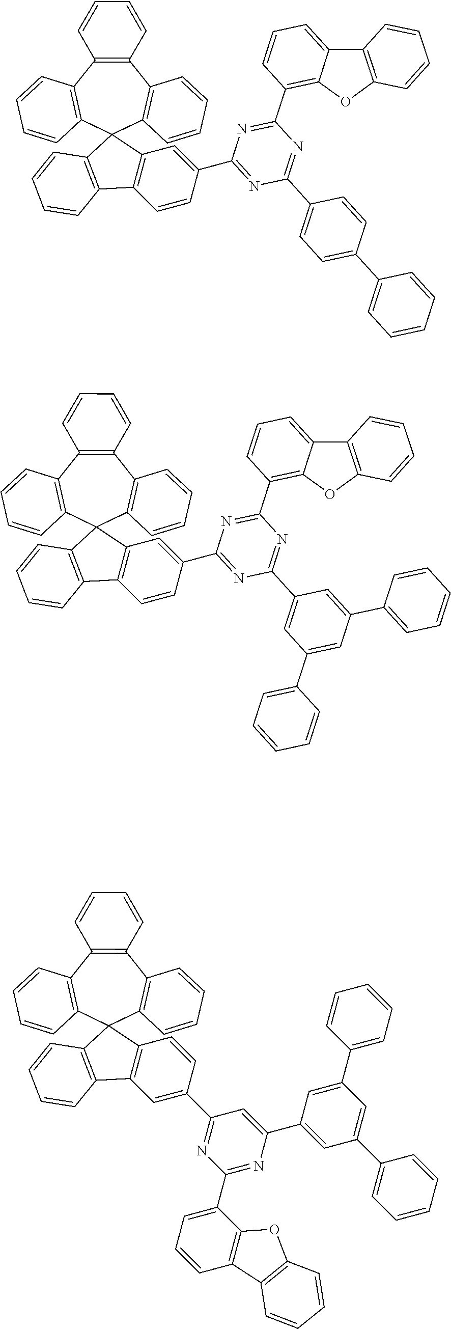


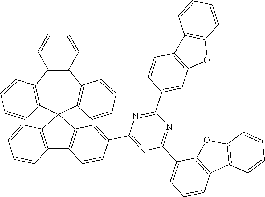


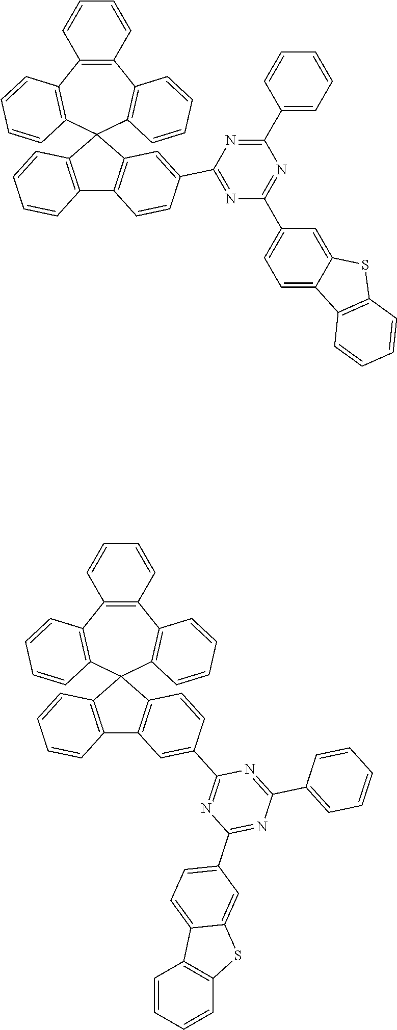


where X′ is O, S, or


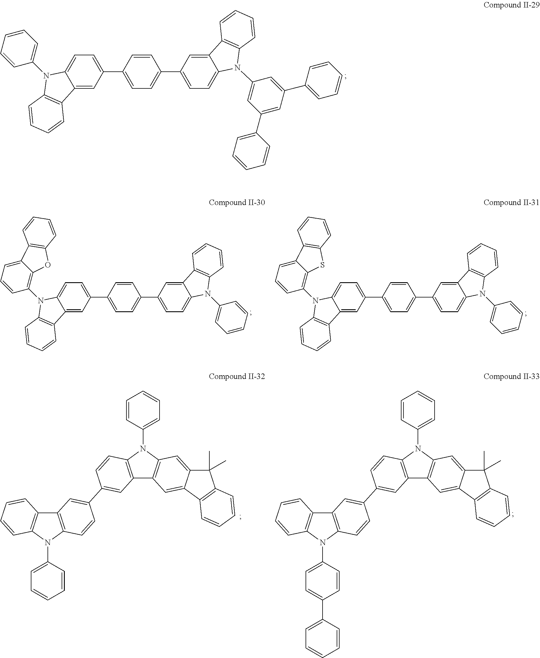


| TABLE 1 |
| chemical structures of the first host compounds |
 |
Compound I-1 |
 |
Compound I-2 |
 |
Compound I-3 |
 |
Compound I-4 |
 |
Compound I-5 |
 |
Compound I-6 |
 |
Compound I-7 |
 |
Compound I-8 |
 |
Compound I-9 |
 |
Compound I-10 |
 |
Compound I-11 |
 |
Compound I-12 |
 |
Compound I-13 |
 |
Compound I-14 |
 |
Compound I-15 |
 |
Compound I-16 |
 |
Compound I-17 |
 |
Compound I-18 |
 |
Compound I-19 |
 |
Compound I-20 |
 |
Compound I-21 |
 |
Compound I-22 |
 |
Compound I-23 |
 |
Compound I-24 |
 |
Compound I-25 |
 |
Compound I-26 |
 |
Compound I-27 |
 |
Compound I-28 |


and Intermediate C2 was


used to synthesize Compound I-10 was synthesized by the following steps. The synthesis pathway was summarized in Scheme R1-1.


in a yield of 80%. Its FD-MS analysis: C21H7D5ClN3O; and observed value of 362.82.
| TABLE 2-1 |
| Intermediate C1 or C2 and Reactant adopted to prepare Compounds |
| I-3 to I-6, I-8 to I-15 and I-28 and their yields, formulae, and FD-MS data |
| Intermediate | First Host Compound |
| C1/ | Reactant/ | Chemical | Yield | Formula/ |
| Intermediate C2 | CAS No. | Structure | (%) | Mass (M+) |
 |
 |
 |
83 | C52H33N3/ 699.84 |
 |
 |
 |
85 | C58H37N3/ 775.93 |
 |
 |
 |
80 | C58H37N3/ 775.93 |
 |
 |
 |
86 | C52H33N3/ 699.84 |
 |
 |
 |
75 | C53H34N2/ 698.85 |
 |
 |
 |
81 | C52H31N3O/ 713.82 |
 |
 |
 |
82 | C52H26D5N3O/ 718.85 |
 |
 |
 |
81 | C58H35N3O/ 789.92 |
 |
 |
 |
75 | C53H32N2O/ 712.83 |
 |
 |
 |
76 | C53H32N2O/ 712.83 |
 |
 |
 |
70 | C53H32N2O/ 712.83 |
 |
 |
 |
79 | C53H32N2O/ 712.83 |
 |
 |
 |
85 | C52H31N3O/ 713.82 |
| TABLE 2-2 |
| H1-NMR results of Compounds I-3 to I-6, I-8 to I-15 and I-28 |
| First Host | |
| Compound | H1-NMR |
 |
1H NMR (500 MHz, CDCl3): δ 9.05 (s, 1H) m 8.79-8.73 (dd, 4H) m 8.43 (dd, 1H),7.91 (d 1H), 7.77-7.46 (m, 18H), 7.47 (t, 1H), 7.46-7.30 (m, 2H), 7.16 (t, 2H), 7.06 (t, 1H), 6.66 (t, 1H), 5.89 (d, 1H) ppm. |
 |
1H NMR (500 MHz, CDCl3): δ 8.81 (s, 2H), 8.69 (d, J = 2.0 Hz, 1H), 8.67 (d, 1H), 8.64 (d, 2H), 7.90-7.85 (m, 2H), 7.8 g-7.75 (m, 2H), 7.75-7.67 (m, 5H), 7.67-7.55 (m, 8H), 7.55-7.50 (m, 4H), 7.50-7.40 (m, 2H), 7.40-7.30 (m, 1H), 7.30-7.20 (m, 3H), 7.13 (t, 1H), 7.09 (t, 1H), 6.64 (t, 1H), 5.89 (d, 1H) ppm. |
 |
1H NMR (500 MHz, CDCl3): δ 8.82 (d, 2H), 8.75-8.65 (m, 2H), 8.61 (d, 2H), 8.00 (s, 1H), 8.60 (d, 2H), 7.80-7.70 (m, 4H), 7.70-7.61 (m, 6H), 7.61-7.51 (m, 7H), 7.51-7.40 (m, 3H), 7.30-7.20 (m, 3H), 7.16 (t, 1H), 7.10 (t, 1H), 6.69 (t, 1H), 5.94 (d, J = 10.5 Hz, 1H) ppm. |
 |
1H NMR (500 MHz, CDCl3): δ 8.94 (s, 1H), 8.75 (d, 4H), 8.73 (d, 1H), 8.01 (d, 1H), 7.91 (d, 1H), 7.79 (dd, 1H), 7.72 (dd, 1H), 7.71 (m, 1H), 7.63-7.52 (m, 14H), 7.40 (dd, 1H), 7.33 (t, 1H), 7.26 (d, 1H), 7.15-7.07 (m, 3H), 6.64 (t, 1H), 5.87 (d, 1H) ppm. |
 |
1H NMR (500 MHz, CDCl3): δ 9.03 (d, 1H), 8.48-8.41 (m, 1H), 8.39 (dd, J = 13, 1H), 8.30-8.24 (m, 2H), 8.21 (d, 1H), 8.02 (s, 1H), 7.91 (d, 1H), 8.03-7.75 (m, 1H), 7.75-7.66 (m, 4H), 7.66-7.58 (m, 6H), 7.58-7.45 (m, 7H), 7.45-7.37 (m, 1H), 7.37-7.26 (m, 2H), 7.19-7.10 (m, 2H), 7.10-7.00 (m, 1H), 6.67 (t, 1H), 5.93 (d, 1H) ppm. |
 |
1H NMR (500 MHz, CDCl3): δ 8.74 (s, 1H), 8.63 (d, 1H), 8.58 (d, 2H), 8.43 (d, 1H), 8.24 (d, 1H), 7.92 (d, 1H), 7.84 (d, 1H), 7.78 (d, 1H), 7.75-7.52 (m, 14H), 7.46 (t, 1H), 7.34 (t, 1H), 7.26 (t, 1H), 7.20-7.05 (m, 3H), 6.65 (t, 1H), 5.90 (d, 1H) ppm. |
 |
1H NMR (500 MHz, CDCl3): δ 8.75 (d, 1H), 8.38 (dd, 1H), 8.46 (d, 1H), 8.25 (d, 1H), 7.93 (d, 1H), 7.84 (d, 1H), 7.78 (d, 1H), 7.75-7.60 (m, 10H), 7.60-7.53 (m, 1H), 7.52-7.44 (m, 1H), 7.35 (t, 3H), 7.29 (d, J = 10.5 Hz, 1H), 7.20-7.05 (m, 3H), 6.70 (t, 1H), 5.92 (d, 1H) ppm. |
 |
1H NMR (500 MHz, CDCl3): δ 9.04 (s, 1H), 8.93 (s, 1H), 8.88 (s, 1H), 8.71 (d, 1H), 8.67 (d, 1H), 8.48 (d, 1H), 8.05-7.85 (m, 3H), 7.84-7.61 (m, 7H), 7.60-7.49 (m, 9H), 7.49-7.26 (m, 3H), 7.20-7.11 (m, 2H), 7.11-7.00 (m, 1H), 6.68 (t, 1H), 5.92 (d, 1H) ppm. |
 |
1H NMR (500 MHz, CDCl3): δ 9.01 (d, 1H), 8.49 (d, 1H), 8.39 (dd, , 1H), 8.30-8.20 (m, 3H), 8.10-8.03 (m, 2H), 7.98 (d, 1H), 7.90 (d, 1H), 7.83-7.73 (m, 1H), 7.72-7.45 (m, 12H), 7.42-7.26 (m, 3H), 7.20-7.10 (m, 2H), 7.09-7.00 (m, 1H), 6.65 (td, 1H), 5.90 (d, 1H) ppm. |
 |
1H NMR (500 MHz, CDCl3): δ 8.66 (d, 2H), 8.39 (s, 1H), 8.20-8.12 (m, 2H), 8.09 (d, 1H), 8.05-7.95 (m, 4H), 7.89-7.80 (m, 2H), 7.80-7.69 (m, 3H), 7.69-7.58 (m, 6H), 7.57-7.50 (m, 4H), 7.39 (t,, 1H), 7.33 (t, 1H), 7.29 (d, 1H), 7.15-7.04 (m, 2H), 6.64 (t, 1H), 5.91 (d, 1H) ppm. |
 |
1H NMR (500 MHz, CDCl3): δ 8.70(dd, J = 10.0, 3.5 Hz, 2H), 8.58 (d, J = 2.5 Hz, 1H), 8.51 (d, 1H), 8.21 (dd, 1H), 8.05 (s, 1H), 8.03-8.01 (m, 1H), 8.00-7.93 (m, 2H), 7.92-7.88 (m, 1H), 7.76-7.70 (m, 2H), 7.70-7.56 (m, 7H), 7.55-7.45 (m, 5H), 7.4-7.26 (m, 3H), 7.20-7.10 (m, 2H), 7.10-7.02 (m, 1H), 6.66 (t, 1H), 5.89 (d, 1H) ppm. |
 |
1H NMR (500 MHz, CDCl3): δ 8.62-8.52(m, 2H), 8.41 (d, 1H), 8.24 (d, J = 2.0 Hz, 1H), 8.20-8.10 (dd, H), 8.04-7.92 (m, 3H), 7.85-7.69 (m, 5H), 7.69-7.57 (m, 7H), 7.57-7.45 (m, 4H), 7.45-7.31 (m, 2H), 7.28 (dd, 1H), 7.19-7.05 (m, 2H), 6.66 (t, 1H), 5.91 (d, 1H) ppm. |
 |
1H NMR (500 MHz, CDCl3): δ 9.17 (s, 1H), 8.73-8.68 (m, 2H), 8.65 (d, 1H), 8.60 (d, 2H), 8.11 (d, 1H), 8.02 (d, 1H), 7.83 (d, 1H), 7.79-7.69 (m, 4H), 7.69-7.61 (m, 6H), 7.61-7.51 (m, 4H), 7.48 (t, 1H), 7.43-7.31 (m, 2H), 7.26 (t, 1H), 7.20-7.05 (m, 2H), 6.67 (t, 1H), 5.90 (d, 1H) ppm. |


and Intermediate C2′ was

| TABLE 3-1 |
| Intermediate C1′ or C2′ and Reactant Bn adopted to prepare |
| Compounds I-16 to I-19 and I-27 and their yields, formulae, and FD-MS data |
| First Host Compound |
| Intermediate C1′/ | Reactant Bn/ | Chemical | Yield | Formula/ |
| Intermediate C2′ | CAS No. | Structure | (%) | Mass (M+) |
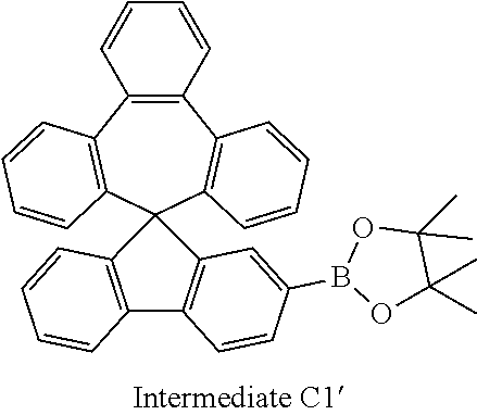 |
 |
 |
85 | C46H29N3/ 623.74 |
 |
 |
 |
65 | C58H37N3/ 775.93 |
 |
 |
 |
77 | C58H37N3/ 775.93 |
 |
 |
 |
82 | C58H37N3/ 775.93 |
 |
 |
 |
76 | C58H37N3/ 775.93 |
| TABLE 3-2 |
| H1-NMR results of Compounds I-16 to I-19 and I-27 |
| First Host | |
| Compound | H1-NMR |
 |
δ 9.01 ppm (d, 1H), 8.99 ppm (s, 1H), 8.75 ppm (d, 4H), 8.65 ppm (d, 1H), 8.05 ppm (d, 1H), 7.7 ppm (t, 2H), 7.60-7.58 ppm (m, 8H), 7.35-7.31 ppm (m, 4H), 7.29-7.05 ppm (m, 5H), 6.70 ppm (t, 1H), 5.85 ppm (d, 1H). |
 |
δ 9.01 ppm (s, 2H), 8.89 ppm (s, 1H), 8.74 ppm (d, 2H), 8.07 ppm (d, 1H), 7.84 ppm (dd, 2H), 7.76-7.68 ppm (m, 6H), 7.66-7.57 ppm (m, 6H),, 7.52-7.46 ppm (m, 5H) 7.44-7.39 ppm (m, 3H), 7.36-7.30 ppm (m, 4H), 7.16 ppm (t, 1H), 7.11-7.06 ppm (m, 2H), 6.70 ppm (t, 1H), 5.89 ppm (d, 1H). |
 |
δ 9.23 ppm (s, 1H), 9.08 ppm (s, 2H), 8.96 ppm (d, 1H), 8.92 ppm (s, 2H), 8.85 ppm (d, 2H), 8.69 ppm (d, 2H), 8.10 ppm (d, 1H), 8.02 ppm (d, 1H), 7.85-7.76 ppm (m, 11H), 7.73-7.67 ppm (m, 10H), 7.64-7.58 ppm (m, 12H), 7.53 ppm (dd, 8H), 7.44 ppm (t, 4H), 7.34 ppm (t, 4H), 7.19-7.12 ppm (m, 6H), 7.05 ppm (t, 4H), 6.69 ppm (t, 1H), 6.05 ppm (d, 1H), 5.85 ppm (d, 1H). |
 |
δ 9.23 ppm (s, 1H), 9.04 ppm (s, 2H), 8.94 ppm (d, IH), 8.92 ppm (s, 1H), 8.88 ppm (s, 2H), 8.86 ppm (d, 2H), 8.73 ppm (d, 2H) 8.10 ppm (d, 1H), 8.19 ppm (s, 1H), 8.02 ppm (d, 1H), 8.00ppm (s, 1H)7.83 ppm (d, 6H), 7.78 ppm (d, 4H), 7.70 ppm (dd, 4H), 7.70-7.51 ppm (m, 25H), 7.46 ppm (t, 4H), 7.34 ppm (t, 4H), 7.20-7.13 ppm (m, 5H), 7.08-7.04 ppm (m, 4H), 6.68 ppm (t, 1H), 6.05 ppm (dd 1H), 5.88 ppm (dd, 1H). |
 |
δ 8.97 ppm (s, 3H), 8.84 ppm (s, 1H), 8.81 ppm (d, 1H), 8.77 ppm (d, 1H), 8.06 ppm (m, 2H), 7.80-7.76 ppm (m, 6H), 7.62-7.49 ppm (m, 12H), 7.47-7.41 ppm (m, 4H), 7.34-7.24 ppm (m, 3H), 7.09-7.05 ppm (m, 2H), 6.68 ppm (t, 1H), 5.87 ppm (d, 1H). |


(Intermediate C1-B),

(Intermediate C2-B),

(Intermediate C7-B), or

(Intermediate C3-B).


(Intermediate D1-B) or

(Intermediate D4-B).
| TABLE 4 |
| chemical structures and CAS No. of the second host compounds |
| Chemical structure |
 |
 |
| CAS No. | [57102-51-9] | [1643479-47-3] |
| Chemical structure |
 |
 |
| CAS No. | [1357150-54-9] | [1541194-36-8] |
| TABLE 5 |
| materials of first and second host compounds and weight ratio |
| therebetween in Compositions 1 to 53 |
| Weight ratio of first | |||
| Composition | First Host | Second Host | and second host |
| No. | Compound | Compound | compounds |
| 1 | Compound I-1 | Compound II-1 | 1:1 |
| 2 | Compound I-2 | Compound II-1 | 1:1 |
| 3 | Compound I-4 | Compound II-1 | 1:1 |
| 4 | Compound I-5 | Compound II-1 | 1:1 |
| 5 | Compound I-9 | Compound II-1 | 1:1 |
| 6 | Compound I-18 | Compound II-1 | 1:1 |
| 7 | Compound I-19 | Compound II-1 | 1:1 |
| 8 | Compound I-20 | Compound II-1 | 1:1 |
| 9 | Compound I-22 | Compound II-1 | 1:1 |
| 10 | Compound I-24 | Compound II-1 | 1:1 |
| 11 | Compound I-26 | Compound II-1 | 1:1 |
| 12 | Compound I-28 | Compound II-1 | 1:1 |
| 13 | Compound I-1 | Compound II-2 | 1:1 |
| 14 | Compound I-2 | Compound II-2 | 1:1 |
| 15 | Compound I-3 | Compound II-2 | 1:1 |
| 16 | Compound I-4 | Compound II-2 | 1:1 |
| 17 | Compound I-5 | Compound II-2 | 1:1 |
| 18 | Compound I-6 | Compound II-2 | 1:1 |
| 19 | Compound I-7 | Compound II-2 | 1:1 |
| 20 | Compound I-8 | Compound II-2 | 1:1 |
| 21 | Compound I-9 | Compound II-2 | 1:1 |
| 22 | Compound I-10 | Compound II-2 | 1:1 |
| 23 | Compound I-11 | Compound II-2 | 1:1 |
| 24 | Compound I-12 | Compound II-2 | 1:1 |
| 25 | Compound I-13 | Compound II-2 | 1:1 |
| 26 | Compound I-14 | Compound II-2 | 1:1 |
| 27 | Compound I-15 | Compound II-2 | 1:1 |
| 28 | Compound I-16 | Compound II-2 | 1:1 |
| 29 | Compound I-17 | Compound II-2 | 1:1 |
| 30 | Compound I-18 | Compound II-2 | 1:1 |
| 31 | Compound I-19 | Compound II-2 | 1:1 |
| 32 | Compound I-20 | Compound II-2 | 1:1 |
| 33 | Compound I-21 | Compound II-2 | 1:1 |
| 34 | Compound I-22 | Compound II-2 | 1:1 |
| 35 | Compound I-23 | Compound II-2 | 1:1 |
| 36 | Compound I-24 | Compound II-2 | 1:1 |
| 37 | Compound I-25 | Compound II-2 | 1:1 |
| 38 | Compound I-26 | Compound II-2 | 1:1 |
| 39 | Compound I-27 | Compound II-2 | 1:1 |
| 40 | Compound I-2 | Compound II-3 | 1:1 |
| 41 | Compound I-7 | Compound II-3 | 1:1 |
| 42 | Compound I-2 | Compound II-4 | 1:1 |
| 43 | Compound I-5 | Compound II-4 | 1:1 |
| 44 | Compound I-12 | Compound II-4 | 1:1 |
| 45 | Compound I-20 | Compound II-4 | 1:1 |
| 46 | Compound I-22 | Compound II-4 | 1:1 |
| 47 | Compound I-18 | Compound II-4 | 1:1 |
| 48 | Compound I-2 | Compound II-1 | 6:4 |
| 49 | Compound I-26 | Compound II-1 | 6:4 |
| 50 | Compound I-5 | Compound II-4 | 6:4 |
| 51 | Compound I-12 | Compound II-4 | 4:6 |
| 52 | TPBi | Compound II-2 | 1:1 |
| 53 | TPBi | Compound II-1 | 1:1 |
| TABLE 6 |
| λmax of |
| to 39, 42, 43, 45 to 47 and 52 and λmax of the |
| first and second host compounds concerned |
| λmax of | |||||
| λmax of | Second | λmax of | |||
| Compo- | Second | First Host | Host | Compo- | |
| sition | First Host | Host | Compound | Compound | sition |
| No. | Compound | Compound | (nm) | (nm) | (nm) |
| 2 | I-2 | II-1 | 393 | 413 | 498 |
| 8 | I-20 | II-1 | 445 | 413 | 493 |
| 9 | I-22 | II-1 | 417 | 413 | 500 |
| 13 | I-1 | II-2 | 394 | 414 | 488 |
| 14 | I-2 | II-2 | 393 | 414 | 478 |
| 16 | I-4 | II-2 | 407 | 414 | 500 |
| 17 | I-5 | II-2 | 419 | 414 | 500 |
| 19 | I-7 | II-2 | 387 | 414 | 462 |
| 28 | I-16 | II-2 | 402 | 414 | 478 |
| 29 | I-17 | II-2 | 404 | 414 | 493 |
| 30 | I-18 | II-2 | 398 | 414 | 494 |
| 31 | I-19 | II-2 | 392 | 414 | 499 |
| 32 | I-20 | II-2 | 445 | 414 | 466 |
| 33 | I-21 | II-2 | 401 | 414 | 488 |
| 34 | I-22 | II-2 | 417 | 414 | 505 |
| 35 | I-23 | II-2 | 397 | 414 | 508 |
| 36 | I-24 | II-2 | 395 | 414 | 494 |
| 37 | I-25 | II-2 | 410 | 414 | 483 |
| 38 | I-26 | II-2 | 389 | 414 | 463 |
| 39 | I-27 | II-2 | 403 | 414 | 498 |
| 42 | I-2 | II-4 | 393 | 388 | 469 |
| 43 | I-5 | II-4 | 419 | 388 | 469 |
| 45 | I-20 | II-4 | 445 | 388 | 472 |
| 46 | I-22 | II-4 | 417 | 388 | 477 |
| 47 | I-18 | II-4 | 398 | 388 | 463 |
| 52 | TPBi | Compound | 382 | 414 | 418 |
| II-2 | |||||
| TABLE 7 |
| chemical structures of commercial materials for OLED devices |
 |
 |
 |
 |
 |
 |
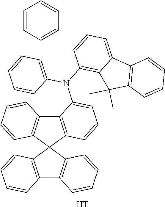 |
 |
| TABLE 8 |
| coating sequence, materials and thickness of the organic layers in |
| green OLED device |
| Coating | ||||
| Sequence | Layer | Material | Thickness | |
| 1 | HIL-1 | HI doped with 3.0 wt % of HI-D | 100 |
|
| 2 | HIL-2 | HI | 1400 Å | |
| 3 | HTL | HT | 100 |
|
| 4 | GEL | Composition for GH doped with 10.0 | 400 Å | |
| wt % of GD | ||||
| 5 | ETL | ET doped with 35.0 wt % of |
350 Å | |
| 6 | | Liq | 15 Å | |
| 7 | Cthd | Al | 1500 Å | |
| TABLE 9 |
| coating sequence, materials and thickness of the |
| organic layers in red OLED device |
| Coating | ||||
| Sequence | Layer | Material | Thickness | |
| 1 | HIL-1 | HI doped with 3.0 wt % of HI-D | 100 |
|
| 2 | HIL-2 | HI | 2200 Å | |
| 3 | HTL | HT | 100 Å | |
| 4 | REL | Composition for RH doped with 3.5 | 300 Å | |
| wt % of RD | ||||
| 5 | ETL | ET doped with 35.0 wt % of |
350 Å | |
| 6 | | Liq | 15 Å | |
| 7 | Cthd | Al | 1500 Å | |
-
- (3). Measurement of Current Efficiency
-
- (4). Measurement of Color Coordinates (x,y)
| TABLE 10 |
| Compositions for GH, CIEs, driving voltages, and current |
| efficiencies of green OLED devices of Examples |
| 1 to 37 and Comparative Example 1 |
| Composition | Driving | Current | ||
| Example | No. | CIE | voltage | efficiency |
| No. | for GH | (x, y) | (V) | (cd/A) |
| Example 1 | 1 | (0.316, 0.632) | 5.24 | 67.3 |
| Example 2 | 2 | (0.319,0.630) | 4.18 | 68.6 |
| Example 3 | 3 | (0.319, 0.629) | 4.45 | 66.6 |
| Example 4 | 4 | (0.322, 0.629) | 4.72 | 68.8 |
| Example 5 | 6 | (0.314, 0.632) | 5.18 | 61.8 |
| Example 6 | 8 | (0.318, 0.628) | 4.60 | 64.1 |
| Example 7 | 9 | (0.322, 0.628) | 4.22 | 62.3 |
| Example 8 | 11 | (0.328, 0.627) | 4.74 | 73.2 |
| Example 9 | 15 | (0.317, 0.634) | 4.29 | 71.8 |
| Example 10 | 18 | (0.356, 0.598) | 5.41 | 58.6 |
| Example 11 | 20 | (0.314, 0.635) | 4.58 | 63.9 |
| Example 12 | 21 | (0.323, 0.629) | 4.14 | 69.2 |
| Example 13 | 22 | (0.330, 0.625) | 4.22 | 70.2 |
| Example 14 | 23 | (0.317, 0.632) | 4.62 | 66.8 |
| Example 15 | 24 | (0.314, 0.635) | 4.59 | 70.4 |
| Example 16 | 25 | (0.324, 0.630) | 4.63 | 70.7 |
| Example 17 | 26 | (0.313, 0.635) | 4.55 | 70.0 |
| Example 18 | 27 | (0.316, 0.634) | 4.40 | 72.3 |
| Example 19 | 28 | (0.318, 0.629) | 4.45 | 65.2 |
| Example 20 | 29 | (0.320, 0.627) | 4.53 | 61.5 |
| Example 21 | 31 | (0.317,0.631) | 4.55 | 65.2 |
| Example 22 | 33 | (0.315, 0.631) | 4.34 | 62.3 |
| Example 23 | 35 | (0.321, 0.625) | 5.75 | 58.9 |
| Example 24 | 36 | (0.318, 0.629) | 4.35 | 66.7 |
| Example 25 | 37 | (0.318, 0.628) | 4.14 | 62.7 |
| Example 26 | 38 | (0.312, 0.633) | 4.53 | 65.5 |
| Example 27 | 40 | (0.317, 0.630) | 5.24 | 61.0 |
| Example 28 | 41 | (0.317, 0.629) | 4.70 | 59.9 |
| Example 29 | 42 | (0.320, 0.627) | 4.62 | 63.0 |
| Example 30 | 43 | (0.322, 0.631) | 4.37 | 72.4 |
| Example 31 | 45 | (0.319, 0.627) | 4.46 | 62.9 |
| Example 32 | 46 | (0.322, 0.627) | 4.34 | 63.7 |
| Example 33 | 47 | (0.316, 0.630) | 5.39 | 61.8 |
| Example 34 | 48 | (0.323, 0.629) | 4.23 | 68.2 |
| Example 35 | 49 | (0.317, 0.633) | 4.37 | 76.1 |
| Example 36 | 50 | (0.331, 0.626) | 4.28 | 73.7 |
| Example 37 | 51 | (0.319, 0.633) | 4.91 | 68.1 |
| Comparative | 53 | (0.313, 0.634) | 6.30 | 47.2 |
| Example 1 | ||||
| TABLE 11 |
| Compositions for RH, CIEs, driving voltages, and current |
| efficiencies of red OLED devices of Examples |
| 38 to 43 and Comparative Example 2 |
| Driving | Current | |||
| Example | Composition | CIE | voltage | efficiency |
| No. | No. for RH | (x, y) | (V) | (cd/A) |
| Example 38 | 5 | (0.660, 0.338) | 4.05 | 27.3 |
| Example 39 | 7 | (0.665, 0.333) | 4.31 | 27.0 |
| Example 40 | 10 | (0.660, 0.338) | 4.31 | 28.7 |
| Example 41 | 12 | (0.661, 0.337) | 4.40 | 26.0 |
| Example 42 | 19 | (0.661, 0.336) | 4.74 | 28.7 |
| Example 43 | 44 | (0.661, 0.336) | 4.53 | 28.2 |
| Comparative | 53 | (0.658, 0.339) | 5.80 | 17.5 |
| Example 2 | ||||
| TABLE 12 |
| Compositions for GH and lifespan of green OLED |
| devices of Examples 1 to 7, 12, 13, 18, 29 to |
| 34, 36 and 37 and Comparative Example 1 |
| Example | Composition | Lifespan (T95) |
| No. | No. | (hrs) |
| Example 1 | 1 | 90 |
| Example 2 | 2 | 104 |
| Example 3 | 3 | 47 |
| Example 4 | 4 | 81 |
| Example 5 | 6 | 65 |
| Example 6 | 8 | 61 |
| Example 7 | 9 | 112 |
| Example 12 | 21 | 40 |
| Example 13 | 22 | 20 |
| Example 18 | 27 | 44 |
| Example 29 | 42 | 112 |
| Example 30 | 43 | 30 |
| Example 31 | 45 | 87 |
| Example 32 | 46 | 98 |
| Example 33 | 47 | 56 |
| Example 34 | 48 | 52 |
| Example 36 | 50 | 68 |
| Example 37 | 51 | 20 |
| Comparative Example 1 | 53 | 1 |
| TABLE 13 |
| Compositions for RH and lifespan of red OLED |
| devices of Examples 38, 39, 41 |
| and 43 and Comparative Example 2 |
| Example | Composition | Lifespan (T95) |
| No. | No. | (hrs) |
| Example 38 | 5 | 32 |
| Example 39 | 7 | 17 |
| Example 41 | 12 | 16 |
| Example 43 | 44 | 14 |
| Comparative Example 2 | 53 | 0.5 |
Claims (19)


Priority Applications (1)
| Application Number | Priority Date | Filing Date | Title |
|---|---|---|---|
| US16/429,124 US11183641B2 (en) | 2018-06-05 | 2019-06-03 | Composition for an organic electronic device and organic electronic device using the same |
Applications Claiming Priority (2)
| Application Number | Priority Date | Filing Date | Title |
|---|---|---|---|
| US201862680625P | 2018-06-05 | 2018-06-05 | |
| US16/429,124 US11183641B2 (en) | 2018-06-05 | 2019-06-03 | Composition for an organic electronic device and organic electronic device using the same |
Publications (2)
| Publication Number | Publication Date |
|---|---|
| US20190372014A1 US20190372014A1 (en) | 2019-12-05 |
| US11183641B2 true US11183641B2 (en) | 2021-11-23 |
Family
ID=68692823
Family Applications (4)
| Application Number | Title | Priority Date | Filing Date |
|---|---|---|---|
| US16/429,124 Expired - Fee Related US11183641B2 (en) | 2018-06-05 | 2019-06-03 | Composition for an organic electronic device and organic electronic device using the same |
| US16/429,563 Abandoned US20190372015A1 (en) | 2018-06-05 | 2019-06-03 | Compound and organic electronic device comprising the same |
| US16/429,160 Abandoned US20190367491A1 (en) | 2018-06-05 | 2019-06-03 | Compound and organic electronic device comprising the same |
| US16/429,594 Abandoned US20190372016A1 (en) | 2018-06-05 | 2019-06-03 | Compound and organic electronic device using the same |
Family Applications After (3)
| Application Number | Title | Priority Date | Filing Date |
|---|---|---|---|
| US16/429,563 Abandoned US20190372015A1 (en) | 2018-06-05 | 2019-06-03 | Compound and organic electronic device comprising the same |
| US16/429,160 Abandoned US20190367491A1 (en) | 2018-06-05 | 2019-06-03 | Compound and organic electronic device comprising the same |
| US16/429,594 Abandoned US20190372016A1 (en) | 2018-06-05 | 2019-06-03 | Compound and organic electronic device using the same |
Country Status (5)
| Country | Link |
|---|---|
| US (4) | US11183641B2 (en) |
| JP (1) | JP6771785B2 (en) |
| KR (4) | KR102170538B1 (en) |
| CN (4) | CN110563662A (en) |
| TW (1) | TWI699357B (en) |
Families Citing this family (4)
| Publication number | Priority date | Publication date | Assignee | Title |
|---|---|---|---|---|
| KR102263106B1 (en) * | 2019-12-19 | 2021-06-09 | 주식회사 엘지화학 | Novel compound and organic light emitting device comprising the same |
| KR102691685B1 (en) | 2020-02-18 | 2024-08-05 | 히다치 아스테모 가부시키가이샤 | Vehicle control device, vehicle control method and vehicle control system |
| CN115745872A (en) * | 2022-09-06 | 2023-03-07 | 常州强力昱镭光电材料有限公司 | Spirofluorene derivative containing seven-membered ring, electron transport material containing the same, and organic electroluminescent element |
| CN119954853A (en) * | 2024-07-15 | 2025-05-09 | 北京云基科技股份有限公司 | A heterocyclic compound and its application |
Citations (4)
| Publication number | Priority date | Publication date | Assignee | Title |
|---|---|---|---|---|
| CN105679946A (en) | 2014-12-09 | 2016-06-15 | 三星Sdi株式会社 | Organic Optoelectronic Devices and Display Devices |
| CN107011248A (en) | 2016-01-27 | 2017-08-04 | 彩丰精技股份有限公司 | Compound and organic electronic device thereof |
| WO2018021714A1 (en) * | 2016-07-26 | 2018-02-01 | 주식회사 엘지화학 | Organic light emitting element |
| US20180155312A1 (en) * | 2016-12-07 | 2018-06-07 | Nichem Fine Technology Co., Ltd. | Compound and organic electronic device using the same |
Family Cites Families (10)
| Publication number | Priority date | Publication date | Assignee | Title |
|---|---|---|---|---|
| JP2008074832A (en) * | 2006-08-24 | 2008-04-03 | Tokuyama Corp | Chromene compounds |
| KR101793428B1 (en) * | 2011-04-13 | 2017-11-03 | 에스에프씨 주식회사 | Condensed aryl compounds and organic light-diode including the same |
| JP6071398B2 (en) * | 2012-10-05 | 2017-02-01 | キヤノン株式会社 | Indeno [1,2-b] phenanthrene compound and organic light-emitting device having the same |
| US10573818B2 (en) * | 2014-12-01 | 2020-02-25 | Merck Patent Gmbh | Materials for organic electroluminescent devices |
| TWI662013B (en) * | 2016-03-24 | 2019-06-11 | 大陸商上海嶸彩光電材料有限公司 | Compound and organic electronic device using the same |
| KR102573815B1 (en) * | 2016-05-09 | 2023-09-04 | 삼성디스플레이 주식회사 | Polycyclic compound and organic electroluminescence device including the same |
| KR102637956B1 (en) * | 2016-08-02 | 2024-02-19 | 에스에프씨 주식회사 | Novel organic compounds derivatives and organic light-emitting diode therewith |
| US10476006B2 (en) * | 2016-08-09 | 2019-11-12 | Shanghai Nichem Fine Chemical Co., Ltd. | Compound and organic electronic device using the same |
| US10693075B2 (en) * | 2016-08-09 | 2020-06-23 | Shanghai Nichem Fine Chemical Co., Ltd. | Spiro compound and organic electronic device comprising the same |
| EP3291319B1 (en) * | 2016-08-30 | 2019-01-23 | Novaled GmbH | Method for preparing an organic semiconductor layer |
-
2019
- 2019-06-03 US US16/429,124 patent/US11183641B2/en not_active Expired - Fee Related
- 2019-06-03 US US16/429,563 patent/US20190372015A1/en not_active Abandoned
- 2019-06-03 US US16/429,160 patent/US20190367491A1/en not_active Abandoned
- 2019-06-03 US US16/429,594 patent/US20190372016A1/en not_active Abandoned
- 2019-06-04 CN CN201910481571.4A patent/CN110563662A/en active Pending
- 2019-06-04 TW TW108119389A patent/TWI699357B/en not_active IP Right Cessation
- 2019-06-04 CN CN201910482237.0A patent/CN110563707A/en active Pending
- 2019-06-04 CN CN201910482238.5A patent/CN110571338B/en active Active
- 2019-06-04 JP JP2019104392A patent/JP6771785B2/en not_active Expired - Fee Related
- 2019-06-05 KR KR1020190066992A patent/KR102170538B1/en not_active Expired - Fee Related
- 2019-06-05 CN CN201910485320.3A patent/CN110563638A/en active Pending
- 2019-06-05 KR KR1020190066952A patent/KR20190138611A/en not_active Ceased
- 2019-06-05 KR KR1020190066983A patent/KR102259757B1/en not_active Expired - Fee Related
- 2019-06-05 KR KR1020190066982A patent/KR102243851B1/en not_active Expired - Fee Related
Patent Citations (5)
| Publication number | Priority date | Publication date | Assignee | Title |
|---|---|---|---|---|
| CN105679946A (en) | 2014-12-09 | 2016-06-15 | 三星Sdi株式会社 | Organic Optoelectronic Devices and Display Devices |
| CN107011248A (en) | 2016-01-27 | 2017-08-04 | 彩丰精技股份有限公司 | Compound and organic electronic device thereof |
| WO2018021714A1 (en) * | 2016-07-26 | 2018-02-01 | 주식회사 엘지화학 | Organic light emitting element |
| TW201807855A (en) | 2016-07-26 | 2018-03-01 | 南韓商Lg化學股份有限公司 | Organic light emitting device |
| US20180155312A1 (en) * | 2016-12-07 | 2018-06-07 | Nichem Fine Technology Co., Ltd. | Compound and organic electronic device using the same |
Also Published As
| Publication number | Publication date |
|---|---|
| CN110563638A (en) | 2019-12-13 |
| KR20190138612A (en) | 2019-12-13 |
| CN110563662A (en) | 2019-12-13 |
| CN110571338A (en) | 2019-12-13 |
| CN110571338B (en) | 2022-03-04 |
| KR102259757B1 (en) | 2021-06-02 |
| KR20190138611A (en) | 2019-12-13 |
| US20190367491A1 (en) | 2019-12-05 |
| KR102170538B1 (en) | 2020-10-28 |
| KR102243851B1 (en) | 2021-04-23 |
| TW202003478A (en) | 2020-01-16 |
| KR20190138615A (en) | 2019-12-13 |
| CN110563707A (en) | 2019-12-13 |
| JP6771785B2 (en) | 2020-10-21 |
| JP2020025080A (en) | 2020-02-13 |
| US20190372015A1 (en) | 2019-12-05 |
| KR20190138613A (en) | 2019-12-13 |
| US20190372014A1 (en) | 2019-12-05 |
| TWI699357B (en) | 2020-07-21 |
| US20190372016A1 (en) | 2019-12-05 |
Similar Documents
| Publication | Publication Date | Title |
|---|---|---|
| US12291543B2 (en) | Boron compound and organic light-emitting diode comprising same | |
| US11469378B2 (en) | Electroluminescent compound and electroluminescent device including the same | |
| US11133472B1 (en) | Organic light-emitting diode having long lifespan, low voltage, and high efficiency property | |
| CN112457844B (en) | Novel compound and organic light-emitting device containing the same | |
| US10312459B2 (en) | Compound and organic electronic device using the same | |
| US9299935B2 (en) | Nitrogen-containing heterocyclic compounds and organic electronic device comprising the same | |
| US20100326526A1 (en) | Emissive aryl-heteroaryl compounds | |
| US12018039B2 (en) | Boron compound, and organic light-emitting diode comprising same | |
| US12114562B2 (en) | Compound for organic light-emitting diode and long lifespan organic light-emitting diode comprising same | |
| US12209083B2 (en) | Polycyclic compound and organic light emitting diode comprising same | |
| US11183641B2 (en) | Composition for an organic electronic device and organic electronic device using the same | |
| US11279693B2 (en) | Organic heterocyclic compound and light-emitting diode comprising same | |
| KR20160068683A (en) | Novel compound and organic electroluminescent device comprising same | |
| US20150171344A1 (en) | Novel compound and electroluminescent device including same | |
| US12133455B2 (en) | Polycyclic compound and organic light emitting diode comprising same | |
| KR20140086880A (en) | Novel organic compound and organic electroluminescent device comprising same | |
| US7455917B2 (en) | Organic compound and organic light emitting device using the same | |
| KR20140070425A (en) | New compounds and organic electronic device using the same | |
| CN114702484A (en) | Organic compound containing azole and application thereof | |
| KR101838504B1 (en) | An electroluminescent compound and an electroluminescent device comprising the same | |
| US10693077B2 (en) | Compound and organic electronic device using the same | |
| KR20130120855A (en) | Using thiophen derivative as hole transporting mateial and organic electroluminescent device using the same | |
| KR101327301B1 (en) | Amine derivative as hole transporting material and organic electroluminescent device using the same | |
| US10693075B2 (en) | Spiro compound and organic electronic device comprising the same | |
| US12048239B2 (en) | Composition for organic optoelectronic device, organic optoelectronic device and display device |
Legal Events
| Date | Code | Title | Description |
|---|---|---|---|
| AS | Assignment |
Owner name: SHANGHAI NICHEM FINE CHEMICAL CO., LTD., CHINA Free format text: ASSIGNMENT OF ASSIGNORS INTEREST;ASSIGNORS:CHEN, CHI-CHUNG;SHIEH, SHWU-JU;LEE, MING-ZER;REEL/FRAME:049342/0081 Effective date: 20190603 |
|
| FEPP | Fee payment procedure |
Free format text: ENTITY STATUS SET TO UNDISCOUNTED (ORIGINAL EVENT CODE: BIG.); ENTITY STATUS OF PATENT OWNER: SMALL ENTITY |
|
| FEPP | Fee payment procedure |
Free format text: ENTITY STATUS SET TO SMALL (ORIGINAL EVENT CODE: SMAL); ENTITY STATUS OF PATENT OWNER: SMALL ENTITY |
|
| STPP | Information on status: patent application and granting procedure in general |
Free format text: DOCKETED NEW CASE - READY FOR EXAMINATION |
|
| STPP | Information on status: patent application and granting procedure in general |
Free format text: NOTICE OF ALLOWANCE MAILED -- APPLICATION RECEIVED IN OFFICE OF PUBLICATIONS |
|
| STPP | Information on status: patent application and granting procedure in general |
Free format text: PUBLICATIONS -- ISSUE FEE PAYMENT VERIFIED |
|
| STCF | Information on status: patent grant |
Free format text: PATENTED CASE |
|
| FEPP | Fee payment procedure |
Free format text: MAINTENANCE FEE REMINDER MAILED (ORIGINAL EVENT CODE: REM.); ENTITY STATUS OF PATENT OWNER: SMALL ENTITY |
|
| LAPS | Lapse for failure to pay maintenance fees |
Free format text: PATENT EXPIRED FOR FAILURE TO PAY MAINTENANCE FEES (ORIGINAL EVENT CODE: EXP.); ENTITY STATUS OF PATENT OWNER: SMALL ENTITY |
|
| STCH | Information on status: patent discontinuation |
Free format text: PATENT EXPIRED DUE TO NONPAYMENT OF MAINTENANCE FEES UNDER 37 CFR 1.362 |
|
| FP | Lapsed due to failure to pay maintenance fee |
Effective date: 20251123 |