US11177324B2 - Display component, display device and display control method - Google Patents
Display component, display device and display control method Download PDFInfo
- Publication number
- US11177324B2 US11177324B2 US15/781,614 US201715781614A US11177324B2 US 11177324 B2 US11177324 B2 US 11177324B2 US 201715781614 A US201715781614 A US 201715781614A US 11177324 B2 US11177324 B2 US 11177324B2
- Authority
- US
- United States
- Prior art keywords
- inter
- sub
- transmission
- unit
- pixel
- Prior art date
- Legal status (The legal status is an assumption and is not a legal conclusion. Google has not performed a legal analysis and makes no representation as to the accuracy of the status listed.)
- Active, expires
Links
Images


Classifications
-
- H01L27/3211—
-
- G—PHYSICS
- G09—EDUCATION; CRYPTOGRAPHY; DISPLAY; ADVERTISING; SEALS
- G09G—ARRANGEMENTS OR CIRCUITS FOR CONTROL OF INDICATING DEVICES USING STATIC MEANS TO PRESENT VARIABLE INFORMATION
- G09G3/00—Control arrangements or circuits, of interest only in connection with visual indicators other than cathode-ray tubes
- G09G3/20—Control arrangements or circuits, of interest only in connection with visual indicators other than cathode-ray tubes for presentation of an assembly of a number of characters, e.g. a page, by composing the assembly by combination of individual elements arranged in a matrix no fixed position being assigned to or needed to be assigned to the individual characters or partial characters
- G09G3/22—Control arrangements or circuits, of interest only in connection with visual indicators other than cathode-ray tubes for presentation of an assembly of a number of characters, e.g. a page, by composing the assembly by combination of individual elements arranged in a matrix no fixed position being assigned to or needed to be assigned to the individual characters or partial characters using controlled light sources
- G09G3/30—Control arrangements or circuits, of interest only in connection with visual indicators other than cathode-ray tubes for presentation of an assembly of a number of characters, e.g. a page, by composing the assembly by combination of individual elements arranged in a matrix no fixed position being assigned to or needed to be assigned to the individual characters or partial characters using controlled light sources using electroluminescent panels
- G09G3/32—Control arrangements or circuits, of interest only in connection with visual indicators other than cathode-ray tubes for presentation of an assembly of a number of characters, e.g. a page, by composing the assembly by combination of individual elements arranged in a matrix no fixed position being assigned to or needed to be assigned to the individual characters or partial characters using controlled light sources using electroluminescent panels semiconductive, e.g. using light-emitting diodes [LED]
- G09G3/3208—Control arrangements or circuits, of interest only in connection with visual indicators other than cathode-ray tubes for presentation of an assembly of a number of characters, e.g. a page, by composing the assembly by combination of individual elements arranged in a matrix no fixed position being assigned to or needed to be assigned to the individual characters or partial characters using controlled light sources using electroluminescent panels semiconductive, e.g. using light-emitting diodes [LED] organic, e.g. using organic light-emitting diodes [OLED]
- G09G3/3225—Control arrangements or circuits, of interest only in connection with visual indicators other than cathode-ray tubes for presentation of an assembly of a number of characters, e.g. a page, by composing the assembly by combination of individual elements arranged in a matrix no fixed position being assigned to or needed to be assigned to the individual characters or partial characters using controlled light sources using electroluminescent panels semiconductive, e.g. using light-emitting diodes [LED] organic, e.g. using organic light-emitting diodes [OLED] using an active matrix
- G09G3/3233—Control arrangements or circuits, of interest only in connection with visual indicators other than cathode-ray tubes for presentation of an assembly of a number of characters, e.g. a page, by composing the assembly by combination of individual elements arranged in a matrix no fixed position being assigned to or needed to be assigned to the individual characters or partial characters using controlled light sources using electroluminescent panels semiconductive, e.g. using light-emitting diodes [LED] organic, e.g. using organic light-emitting diodes [OLED] using an active matrix with pixel circuitry controlling the current through the light-emitting element
-
- G—PHYSICS
- G09—EDUCATION; CRYPTOGRAPHY; DISPLAY; ADVERTISING; SEALS
- G09G—ARRANGEMENTS OR CIRCUITS FOR CONTROL OF INDICATING DEVICES USING STATIC MEANS TO PRESENT VARIABLE INFORMATION
- G09G3/00—Control arrangements or circuits, of interest only in connection with visual indicators other than cathode-ray tubes
- G09G3/20—Control arrangements or circuits, of interest only in connection with visual indicators other than cathode-ray tubes for presentation of an assembly of a number of characters, e.g. a page, by composing the assembly by combination of individual elements arranged in a matrix no fixed position being assigned to or needed to be assigned to the individual characters or partial characters
- G09G3/22—Control arrangements or circuits, of interest only in connection with visual indicators other than cathode-ray tubes for presentation of an assembly of a number of characters, e.g. a page, by composing the assembly by combination of individual elements arranged in a matrix no fixed position being assigned to or needed to be assigned to the individual characters or partial characters using controlled light sources
- G09G3/30—Control arrangements or circuits, of interest only in connection with visual indicators other than cathode-ray tubes for presentation of an assembly of a number of characters, e.g. a page, by composing the assembly by combination of individual elements arranged in a matrix no fixed position being assigned to or needed to be assigned to the individual characters or partial characters using controlled light sources using electroluminescent panels
- G09G3/32—Control arrangements or circuits, of interest only in connection with visual indicators other than cathode-ray tubes for presentation of an assembly of a number of characters, e.g. a page, by composing the assembly by combination of individual elements arranged in a matrix no fixed position being assigned to or needed to be assigned to the individual characters or partial characters using controlled light sources using electroluminescent panels semiconductive, e.g. using light-emitting diodes [LED]
- G09G3/3208—Control arrangements or circuits, of interest only in connection with visual indicators other than cathode-ray tubes for presentation of an assembly of a number of characters, e.g. a page, by composing the assembly by combination of individual elements arranged in a matrix no fixed position being assigned to or needed to be assigned to the individual characters or partial characters using controlled light sources using electroluminescent panels semiconductive, e.g. using light-emitting diodes [LED] organic, e.g. using organic light-emitting diodes [OLED]
- G09G3/3225—Control arrangements or circuits, of interest only in connection with visual indicators other than cathode-ray tubes for presentation of an assembly of a number of characters, e.g. a page, by composing the assembly by combination of individual elements arranged in a matrix no fixed position being assigned to or needed to be assigned to the individual characters or partial characters using controlled light sources using electroluminescent panels semiconductive, e.g. using light-emitting diodes [LED] organic, e.g. using organic light-emitting diodes [OLED] using an active matrix
- G09G3/3258—Control arrangements or circuits, of interest only in connection with visual indicators other than cathode-ray tubes for presentation of an assembly of a number of characters, e.g. a page, by composing the assembly by combination of individual elements arranged in a matrix no fixed position being assigned to or needed to be assigned to the individual characters or partial characters using controlled light sources using electroluminescent panels semiconductive, e.g. using light-emitting diodes [LED] organic, e.g. using organic light-emitting diodes [OLED] using an active matrix with pixel circuitry controlling the voltage across the light-emitting element
-
- H01L51/5203—
-
- H—ELECTRICITY
- H10—SEMICONDUCTOR DEVICES; ELECTRIC SOLID-STATE DEVICES NOT OTHERWISE PROVIDED FOR
- H10K—ORGANIC ELECTRIC SOLID-STATE DEVICES
- H10K50/00—Organic light-emitting devices
- H10K50/80—Constructional details
- H10K50/805—Electrodes
-
- H—ELECTRICITY
- H10—SEMICONDUCTOR DEVICES; ELECTRIC SOLID-STATE DEVICES NOT OTHERWISE PROVIDED FOR
- H10K—ORGANIC ELECTRIC SOLID-STATE DEVICES
- H10K59/00—Integrated devices, or assemblies of multiple devices, comprising at least one organic light-emitting element covered by group H10K50/00
- H10K59/30—Devices specially adapted for multicolour light emission
- H10K59/35—Devices specially adapted for multicolour light emission comprising red-green-blue [RGB] subpixels
-
- G—PHYSICS
- G02—OPTICS
- G02F—OPTICAL DEVICES OR ARRANGEMENTS FOR THE CONTROL OF LIGHT BY MODIFICATION OF THE OPTICAL PROPERTIES OF THE MEDIA OF THE ELEMENTS INVOLVED THEREIN; NON-LINEAR OPTICS; FREQUENCY-CHANGING OF LIGHT; OPTICAL LOGIC ELEMENTS; OPTICAL ANALOGUE/DIGITAL CONVERTERS
- G02F2201/00—Constructional arrangements not provided for in groups G02F1/00 - G02F7/00
- G02F2201/12—Constructional arrangements not provided for in groups G02F1/00 - G02F7/00 electrode
- G02F2201/121—Constructional arrangements not provided for in groups G02F1/00 - G02F7/00 electrode common or background
-
- G—PHYSICS
- G02—OPTICS
- G02F—OPTICAL DEVICES OR ARRANGEMENTS FOR THE CONTROL OF LIGHT BY MODIFICATION OF THE OPTICAL PROPERTIES OF THE MEDIA OF THE ELEMENTS INVOLVED THEREIN; NON-LINEAR OPTICS; FREQUENCY-CHANGING OF LIGHT; OPTICAL LOGIC ELEMENTS; OPTICAL ANALOGUE/DIGITAL CONVERTERS
- G02F2201/00—Constructional arrangements not provided for in groups G02F1/00 - G02F7/00
- G02F2201/12—Constructional arrangements not provided for in groups G02F1/00 - G02F7/00 electrode
- G02F2201/123—Constructional arrangements not provided for in groups G02F1/00 - G02F7/00 electrode pixel
-
- H01L27/3265—
-
- H—ELECTRICITY
- H10—SEMICONDUCTOR DEVICES; ELECTRIC SOLID-STATE DEVICES NOT OTHERWISE PROVIDED FOR
- H10K—ORGANIC ELECTRIC SOLID-STATE DEVICES
- H10K59/00—Integrated devices, or assemblies of multiple devices, comprising at least one organic light-emitting element covered by group H10K50/00
- H10K59/10—OLED displays
- H10K59/12—Active-matrix OLED [AMOLED] displays
- H10K59/121—Active-matrix OLED [AMOLED] displays characterised by the geometry or disposition of pixel elements
- H10K59/1216—Active-matrix OLED [AMOLED] displays characterised by the geometry or disposition of pixel elements the pixel elements being capacitors
Definitions
- Embodiments of the present disclosure relate to a display component, a display device and a display control method.
- VR Virtual Reality
- An embodiment of the present disclosure provides a display component, including: a plurality of sub-pixel units arranged in a matrix; an inter-transmission connection portion; and a control portion, wherein each sub-pixel unit includes a storage capacitor and an inter-transmission switching element, in each sub-pixel unit, the storage capacitor is connected to the inter-transmission connection portion via the inter-transmission switching element, the control portion is configured to execute at least one inter-transmission operation in one frame period, and each inter-transmission operation includes: selecting at least one sub-pixel unit as a first inter-transmission unit; selecting at least another one sub-pixel unit as a second inter-transmission unit; controlling the storage capacitor of the at least one sub-pixel unit selected as the first inter-transmission unit to discharge; and simultaneously turning on the inter-transmission switching elements of the sub-pixel units selected as the first inter-transmission unit and the second inter-transmission unit, so that the storage capacitor of the at least another one sub-pixel unit selected as the second inter-transmission unit charges the storage capacitor of the at least one sub
- control portion is configured to execute the selecting at least one sub-pixel unit as the first inter-transmission unit and the selecting at least another one sub-pixel unit as the second inter-transmission unit by performing analysis on a frame image signal of the one frame period and a frame image signal of a previous frame period adjacent to the one frame period, wherein a sub-image displayed in the previous frame period of the one frame period by the second inter-transmission unit and a sub-image displayed in the one frame period by the first inter-transmission unit belong to a same position of a same pattern.
- the display component further includes an adjusting unit, the control portion being further configured to adjust the storage capacitor of the at least one sub-pixel unit selected as the first inter-transmission unit by the adjusting unit to have a second voltage.
- the adjusting unit is provided with an input terminal and an output terminal, the input terminal is connected to the control portion, and the output terminal is directly connected to the inter-transmission connection portion.
- a number of the at least one sub-pixel unit selected as the first inter-transmission unit is N
- the plurality of sub-pixel units are formed on a base substrate, and the base substrate is a monocrystalline silicon chip.
- each sub-pixel unit further includes a driving transistor and an Organic Light-Emitting Diode (OLED) element, the driving transistor is connected to the OLED element, and the storage capacitor is configured to maintain a gate voltage of the driving transistor.
- OLED Organic Light-Emitting Diode
- control portion is further configured to execute a charging and/or discharging operation on the storage capacitors of the sub-pixel units which are not selected as the first inter-transmission unit by the at least one inter-transmission operation in the one frame period.
- control portion is further configured to control charge or discharge of the storage capacitor of each sub-pixel unit in a point-to-point manner.
- Another embodiment of the present disclosure provides a display device, including the display component described above.
- Yet another embodiment of the present disclosure provides a display control method of a display device, wherein the display device includes a plurality of sub-pixel units arranged in a matrix and an inter-transmission connection portion, wherein each sub-pixel unit includes a storage capacitor and an inter-transmission switching element, and in each sub-pixel unit, the storage capacitor is connected to the inter-transmission connection portion via the inter-transmission switching element, the display control method including: executing at least one inter-transmission operation in one frame period, each inter-transmission operation including: selecting at least one sub-pixel unit as a first inter-transmission unit; selecting at least another one sub-pixel unit as a second inter-transmission unit; controlling the storage capacitor of the at least one sub-pixel unit selected as the first inter-transmission unit to discharge; and simultaneously turning on the inter-transmission switching elements of the sub-pixel units selected as the first inter-transmission unit and the second inter-transmission unit, so that the storage capacitor of the at least another one sub-pixel unit selected as the second inter-transmission unit charges the storage capacitor
- the selecting at least one sub-pixel unit as the first inter-transmission unit and the selecting at least another one sub-pixel unit as the second inter-transmission unit are executed by analyzing a frame image signal of the one frame period and a frame image signal of a previous frame period adjacent to the one frame period, wherein a sub-image displayed in the previous frame period of the one frame period by the second inter-transmission unit and a sub-image displayed in the one frame period by the first inter-transmission unit belong to a same position of a same pattern.
- each inter-transmission operation further includes: after simultaneously turning on the inter-transmission switching elements selected as the first inter-transmission unit and the second inter-transmission unit, adjusting the storage capacitor of the at least one sub-pixel unit selected as the first inter-transmission unit to have a second voltage.
- a number of the at least one sub-pixel unit selected as the first inter-transmission unit is N
- the display control method further includes: executing a charging and/or discharging operation on the storage capacitors of the sub-pixel units which are not selected as the first inter-transmission units by the at least one inter-transmission operation in the one frame period.
- each sub-pixel unit further includes a driving transistor and an OLED element, a drain electrode of the driving transistor is connected to the OLED element, and the storage capacitor is configured to maintain a gate voltage of the driving transistor.
- each inter-transmission operation further includes: after adjusting the storage capacitor of the at least one sub-pixel unit selected as the first inter-transmission unit to have the second voltage, maintaining the second voltage unmodified in remaining time of the one frame period.
- FIG. 1 shows a schematic diagram of layout of a plurality of sub-pixel units and a plurality of inter-transmission connection portions of a display component provided by an embodiment of the present disclosure.
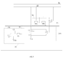
- FIG. 2 shows a schematic diagram of constitution parts of a display component and a connection relationship thereof, as provided by an example of the embodiment of the present disclosure.
- FIG. 3 shows a schematic diagram of constitution parts of a display component and a connection relationship thereof, as provided by another example of an embodiment of the present disclosure.
- FIG. 4 shows a flow chart of a display control method of a display device, as provided by an embodiment of the present disclosure.
- Embodiments of the present disclosure provide a display device and a display control method, which can implement reduction of a transmission amount of external data by data transmission between sub-pixels so as to solve a problem of ultra-large-scale data transmission in a case of a high resolution and a high refresh rate.
- FIG. 1 shows a schematic diagram of layout of a plurality of sub-pixel units and a plurality of inter-transmission connection parts of a display component provided by an embodiment of the present disclosure.
- FIG. 2 shows a schematic diagram of respective constitution parts of a display component and a connection relationship thereof, as provided by an example of the embodiment of the present disclosure.
- the display component provided by the embodiment of the present disclosure is, for example, a display substrate, including a base substrate BS and a plurality of sub-pixel units, first to third inter-transmission connection portions P 1 to P 3 , a control portion 10 and an adjusting portion 20 which are formed on the base substrate BS.
- the base substrate BS is a monocrystalline silicon wafer. It can be understood that the embodiment of the present disclosure does not limit a type of the base substrate, and for example, the base substrate BS can also be a glass substrate.
- the control portion 10 includes one or more Complementary Metal Oxide Semiconductor (CMOS) Integrated Circuits (ICs).
- CMOS Complementary Metal Oxide Semiconductor
- ICs Integrated Circuits
- the embodiment of the present disclosure does not limit a forming position of the control portion 10 either.
- the control portion 10 can be totally formed on the base substrate BS.
- the control portion 10 is an IC, including a logic circuit positioned on the base substrate. The logic circuit is configured to convert digital information into a control signal to control each switch to be turned on/off.
- the control portion 10 can have a portion formed on the base substrate BS, and another portion formed outside the base substrate BS.
- control portion 10 may not be formed on the base substrate BS at all, and for example, the control portion 10 is communicatively connected with respective sub-pixel units SPX and/or a plurality of storage units ST in a wireless manner.
- a plurality of sub-pixel units SPX are arranged in a matrix.
- the plurality of sub-pixel units SPX include a plurality of red sub-pixel units R (1, 1) to R (n, m) arranged in a matrix, a plurality of green sub-pixel units G (1, 1) to G (n, m) arranged in a matrix, and a plurality of blue sub-pixel units B (1, 1) to B (n, m) arranged in a matrix.
- the corresponding red sub-pixel unit R (x, y), green sub-pixel unit G (x, y) and blue sub-pixel unit B (x, y) form a pixel unit PX (x, y).
- the red sub-pixel unit R (1, 1), the green sub-pixel unit G (1, 1) and the blue sub-pixel unit B (1, 1) form a pixel unit PX (1, 1).
- the former reference sign in the brackets represents a row number
- the latter reference sign in the brackets represents a column number.
- each of the red sub-pixel unit R (1, 1) to R (n, m) is connected to the first inter-transmission connection portion P 1 via one inter-transmission switching element SW.
- the inter-transmission switching elements SW of any two red sub-pixels are turned on, the any two red pixels are communicated with each other via the first inter-transmission connection portion P 1 ; and each of the green sub-pixel units G (1, 1) to G (n, m) is connected to the second inter-transmission connection portion P 2 via one inter-transmission switching element SW.
- the inter-transmission switching elements SW of any two green sub-pixels are turned on, the any two green pixels are communicated with each other via the second inter-transmission connection portion P 2 ; and each of the blue sub-pixel units B (1, 1) to B (n, m) is connected to the third inter-transmission connection portion P 3 via one inter-transmission switching element SW.
- the inter-transmission switching elements SW of any two blue sub-pixels are turned on, the two random blue pixels are communicated with each other via the third inter-transmission connection portion P 3 .
- the first inter-transmission connection portion P 1 , the second inter-transmission connection portion P 2 and the third inter-transmission connection portion P 3 may include wires and through holes.
- inter-transmission switching element SW is turned on means that the inter-transmission switching element SW is in a state of allowing current to pass through the inter-transmission switching element SW.
- inter-transmission switching element SW is turned off means that the inter-transmission switching element SW is in a state of not allowing a current to pass through the inter-transmission switching element SW.
- FIG. 2 only schematically shows a connection relationship of one red sub-pixel unit and the first inter-transmission connection portion P 1 as well as other portions of the display substrate. It can be understood that other red sub-pixel units can have a similar structure and connection relationship; the green sub-pixel unit can have a similar structure and can have a corresponding connection relationship with the second inter-transmission connection portion and other portions of the display substrate; and the blue sub-pixel unit can have a similar structure and may also have a corresponding connection relationship with the third inter-transmission connection portion and other portions of the display substrate.
- the sub-pixel unit SPX is an Organic Light-Emitting Diode (OLED) display sub-pixel unit, including a storage capacitor Cst, a driving transistor T 1 and an OLED element.
- the storage capacitor Cst is configured to maintain a gate voltage of the driving transistor T 1 , so that the OLED element can continuously emit light.
- a first electrode E 1 of the storage capacitor Cst is electrically connected to a gate electrode of the driving transistor T 1
- a second electrode E 2 of the storage capacitor Cst is connected to a source electrode of the driving transistor T 1 .
- the storage capacitors of respective sub-pixel units connected to the same inter-transmission connection portion have the same capacitance.
- the control portion 10 is configured to provide a signal (for example, an analog voltage signal) to the respective sub-pixel unit to charge the storage capacitor Cst therein so as to drive the corresponding OLED element to emit light. Further, the control portion 10 , for example, is configured to directly provide a signal (for example, a voltage signal) to each sub-pixel unit to discharge the storage capacitor Cst therein. In the embodiment, the control portion 10 , for example, is configured to control charging and discharging of the storage capacitors of the plurality of sub-pixel units in a point-to-point manner. Namely, the storage capacitor of each sub-pixel unit can independently be charged and discharged regardless of charging or discharging of storage capacitors of other sub-pixel units.
- a signal for example, an analog voltage signal
- the control portion 10 provides an electrical signal to the red sub-pixel unit SPX to charge the storage capacitor Cst.
- the driving transistor T 1 When a voltage between the two electrodes of the storage capacitor Cst exceeds a certain threshold, the driving transistor T 1 is turned on, and the current can flow through the OLED element so as to enable the OLED element to emit light; and in a case that the control portion 10 stops providing the electrical signal to the storage capacitor Cst, the storage capacitor Cst can maintain the gate voltage of the driving transistor T 1 , and thus, the OLED element can continuously emit light in remaining time of one frame period.
- one frame period for example, means time required for producing or displaying one frame of image.
- the inter-transmission switching element SW for example, is a transistor (for example, a Metal Oxide Semiconductor (MOS) transistor).
- MOS Metal Oxide Semiconductor
- the first electrode of the storage capacitor Cst of the sub-pixel unit SPX is connected to the corresponding inter-transmission connection portion via the inter-transmission switching element SW.
- the first electrode of the storage capacitor Cst of the red sub-pixel unit SPX is connected to the first inter-transmission connection portion P 1 via the inter-transmission switching element SW.
- the inter-transmission switching element SW is provided with a source electrode, a drain electrode and a gate electrode.
- the source electrode of the inter-transmission switching element SW is connected to the first electrode of the storage capacitor
- the drain electrode is connected to the first inter-transmission connection portion P 1
- the gate electrode is connected to the control portion 10 .
- the control portion 10 is configured to provide the electrical signal (for example, the voltage signal) to the gate electrode of each inter-transmission switching element SW to turn on each inter-transmission switching element SW, so that the current can flow to the drain electrode from the source electrode of the inter-transmission switching element SW. It can be understood that in a case that the inter-transmission switching element SW is turned on, the current can also flow to the source electrode from the drain electrode of the inter-transmission switching element SW.
- the adjusting portion 20 is configured to adjust a voltage between the first electrode and the second electrode of the storage capacitor Cst of the sub-pixel unit SPX.
- the adjusting portion 20 includes a capacitor C 1 and a transistor T 2 .
- a compensatory voltage signal Vcomp accepted by a source electrode of the transistor T 2 can be stored into the capacitor C 1 , and one electrode of the capacitor C 1 , as an output terminal of the adjusting portion 20 , is directly connected to the first inter-transmission connection portion P 1 .
- the adjusting portion 20 can adjust the voltage between the two electrodes of the storage capacitor Cst of the sub-pixel unit SPX.
- control portion 10 is configured to adjust the voltage between the two electrodes of the storage capacitor Cst of each of the red sub-pixel units connected to the first inter-transmission connection portion P 1 by the adjusting portion 20 .
- the display substrate provided by the embodiment can further include another two adjusting portions (not shown) similar with the adjusting portion 20 , which are respectively connected to the second inter-transmission connection portion P 2 and the third inter-transmission connection portion P 3 . It can be understood that the embodiment of the present disclosure does not limit the number and a circuit structure of the adjusting portion. In another example, one adjusting portion can be provided for each sub-pixel unit.
- one pixel unit includes three sub-pixel units in the above-mentioned embodiment, it can be understood that the number of the sub-pixel units included in one pixel unit is not limited in the embodiment of the present disclosure.
- one pixel unit of a display substrate provided by an embodiment of the present disclosure can include one or four sub-pixel units. In a case that one pixel unit only includes one sub-pixel unit, the sub-pixel unit can be considered as the pixel unit.
- FIG. 3 shows a schematic diagram of respective constitution parts of a display component and a connection relationship thereof, as provided by another example of the embodiment of the present disclosure.
- the same reference signs represent the same or similar elements.
- the adjusting portion 20 includes a magnifier L 1 , a resistance element R 1 and a capacitor C 2 .
- An output terminal M 1 of the adjusting portion 20 is directly connected to the first inter-transmission connection portion P 1 , and input terminals M 2 and M 3 of the adjusting portion 20 are connected to the control portion 10 .
- the inter-transmission switching element SW includes two transistors SW 1 and SW 2 . Gate electrodes of the transistors SW 1 and SW 2 are respectively connected to the control portion 10 .
- the control portion 10 is configured to turn on the inter-transmission switching element SW by providing signals to the gate electrodes of the transistors SW 1 and SW 2 .
- the control portion 10 is configured to simultaneously turn on the transistors SW 1 and SW 2 by respectively providing a row addressing signal and a column addressing signal to the transistors SW 1 and SW 2 , so as to implement turning-on of the inter-transmission switching element SW.
- the sub-pixel unit SPX is, for example, a Liquid Crystal Display (LCD) sub-pixel unit, and includes the storage capacitor Cst.
- the first electrode E 1 of the storage capacitor Cst is, for example, a pixel electrode
- the second electrode E 2 is, for example, a common electrode and/or a common electrode line.
- the storage capacitor Cst is configured to stabilize a written data voltage, i.e., a potential of a pixel electrode.
- the control portion 10 is configured to control the storage capacitor Cst in the sub-pixel SPX to discharge by a discharge control portion formed by transistors T 3 and T 4 .
- the control portion 10 provides the row addressing signal and the column addressing signal to a gate electrode of the transistor SW 1 and a gate electrode of the transistor T 3 , so that the transistor SW 1 and the transistor T 3 are simultaneously turned on, and the transistor T 4 is also turned on, thereby implementing discharging of the storage capacitor Cst.
- the inter-transmission switching element SW is shown outside a dotted box of the sub-pixel unit SPX, but due to that each sub-pixel unit SPX is equipped with one inter-transmission switching element SW, the inter-transmission switching element SW can also be considered as a portion of the sub-pixel unit SPX.
- An embodiment of the present disclosure provides a display device, including the display component provided by any one of the above-mentioned embodiments.
- the display device can be a silicon-based micro display device.
- the display device for example, includes the display component provided by any one of the above-mentioned embodiments.
- the display control method includes: executing an inter-transmission operation at least one time in one frame period, each inter-transmission operation including:
- S 100 selecting at least one sub-pixel unit as a first inter-transmission unit, and selecting at least another one sub-pixel unit as a second inter-transmission unit;
- the selecting at least one sub-pixel unit as the first inter-transmission unit and the selecting at least another one sub-pixel unit as the second inter-transmission unit are executed by carrying out analysis on a frame image signal of the one frame period and a frame image signal of a previous frame period adjacent to the one frame period, wherein a sub-image displayed in the previous frame period of the one frame period by the second inter-transmission unit and a sub-image displayed in the one frame period by the first inter-transmission unit belong to the same position of the same pattern.
- a first frame period is a previous frame period immediately adjacent to a second frame period.
- a second sub-image to be displayed in the second frame period by a plurality of sub-pixel units at a first position and a first sub-image to be displayed in the first frame period by a plurality of sub-pixel units at a second position have a same or similar pattern(s)), for example, a same or similar triangular shape.
- the first position is different from the second position; the similar patterns refer to that one pattern is a pattern obtained by zooming in or zooming out the other pattern in equal proportion.
- the sub-pixel units at positions where a same portion of the same or similar pattern(s) is displayed within the first frame period and the second frame period can be respectively selected as the second inter-transmission unit and the first inter-transmission unit.
- the sub-pixel unit at an upper vertex of a triangle to be displayed in the second frame period can be selected as the first inter-transmission unit
- the sub-pixel unit at the same upper vertex of the triangle to be displayed in the first frame period can be selected as the second inter-transmission unit.
- At least one of the information on the number of sub-pixel units that differs in a row direction and in a column direction between the first inter-transmission unit and the second inter-transmission unit, the information on proportion for zooming in or zooming out the similar pattern, and the information on the number of sub-pixel units of the same or similar pattern occupying in the row direction and in the column direction can also be obtained by the above-described analysis.
- positioning of the first inter-transmission unit can be executed in combination with the at least one of the information described above.
- the display control method includes: executing one inter-transmission operation in one frame period.
- the first frame period and the second frame period represent two adjacent frame periods, i.e., a time point when the first frame period ends is a time point when the second frame period starts.
- the display control method can include: executing two inter-transmission operations in the second frame period as follows.
- the first inter-transmission operation includes:
- Controlling the storage capacitor Cst of the sub-pixel unit R (n ⁇ 1, m) selected as the first inter-transmission unit to discharge i.e., making a voltage (i.e., a voltage between the two electrodes) of the storage capacitor Cst of the sub-pixel unit R (n ⁇ 1, m) become basically 0V (volt).
- the control portion 10 directly provides a discharge signal to the electrode E 1 of the storage capacitor Cst of the sub-pixel unit R (n ⁇ 1, m) so as to enable the storage capacitor Cst of the sub-pixel unit R (n ⁇ 1, m) to discharge.
- FIG. 2 directly provides a discharge signal to the electrode E 1 of the storage capacitor Cst of the sub-pixel unit R (n ⁇ 1, m) so as to enable the storage capacitor Cst of the sub-pixel unit R (n ⁇ 1, m) to discharge.
- control portion 10 for example, by respectively providing a row addressing signal and a column addressing signal to gate electrodes of the transistors SW 1 and T 3 of the sub-pixel unit R (n ⁇ 1, m), makes the storage capacitor Cst of the sub-pixel unit R (n ⁇ 1, m) to discharge via the transistor T 4 .
- the case that the storage capacitor Cst of the sub-pixel unit R (n ⁇ 1, m) is charged to have the voltage V 1 means that the storage capacitor Cst of the sub-pixel unit R (n ⁇ 1, m) is charged to have the voltage V 1 between the two electrodes E 1 and E 2 of the storage capacitor Cst.
- the storage capacitor Cst of the sub-pixel unit R (n ⁇ 1, m) selected as the first inter-transmission unit and the storage capacitor Cst of the sub-pixel unit R (1, 1) selected as the second inter-transmission unit are connected in series.
- the control portion 10 directly provides addressing signals to the inter-transmission switching elements SW of the sub-pixel units R (1, 1) and R (n ⁇ 1, m) so as to turn on the inter-transmission switching elements SW of the sub-pixel units R (1, 1) and R (n ⁇ 1, m).
- the control portion 10 for example, by respectively providing a row addressing signal and a column addressing signal to the gate electrodes of the transistors SW 1 and SW 2 of each of the sub-pixel units R (1, 1) and R (n ⁇ 1, m), turns on the inter-transmission transistor SW of each of the sub-pixel units R (1, 1) and R (n ⁇ 1, m).
- the voltage between the two electrodes of the storage capacitor Cst of the sub-pixel unit R (1, 1) selected as the second inter-transmission unit is 3V.
- the voltage between the two electrodes of the storage capacitor Cst is basically 0V. Simultaneously turn-on of the inter-transmission switching elements of the sub-pixel units R (1, 1) and R (n ⁇ 1, m) enables the storage capacitors of the sub-pixel units R (1, 1) and R (n ⁇ 1, m) to be connected in series via the first inter-transmission portion P 1 .
- the second inter-transmission operation includes:
- Controlling the storage capacitor Cst of the sub-pixel unit R (n, m) selected as the first inter-transmission unit to discharge i.e., making the voltage of the storage capacitor Cst of the sub-pixel unit R (n, m) become basically 0V (volt).
- the storage capacitor Cst of the sub-pixel unit R (2, 1) selected as the second inter-transmission unit charges the storage capacitor Cst of the sub-pixel unit R (n, m) selected as the first inter-transmission unit to enable the storage capacitor Cst of the sub-pixel unit R (n, m) to have the voltage V 1 .
- the voltage between the two electrodes of the storage capacitor Cst of the sub-pixel unit R (2, 1) selected as the second inter-transmission unit is 6V.
- the voltage between the two electrodes of the storage capacitor Cst is basically 0V.
- the inter-transmission switching elements of the sub-pixel units R (2, 1) and R (n, m) are simultaneously turned on and the storage capacitors of the sub-pixel units R (2, 1) and R (n, m) are electrically communicated via the first inter-transmission portion P 1 , the voltage between the two electrodes of the storage capacitor of each of the sub-pixel units R (2, 1) and R (n, m) is 3V.
- first inter-transmission operation and the second inter-transmission operation are not carried out simultaneously so as to avoid inter-transmission signal crosstalk.
- the sub-images at the positions of the sub-pixel units R (1, 1) and R (2, 1) in the first frame period are translated to the positions of the sub-pixel units R (n ⁇ 1, m) and R (n, m) to display. Therefore, data signals which originally are to be written into the sub-pixel units R (n ⁇ 1, m) and R (n, m) in the second frame period can be removed, so that the transmission amount of the external data is reduced, and the problem of ultra-large-scale data transmission in a case of a high resolution and a high refresh rate is solved.
- the external data for example, means data outside the sub-pixels.
- the sub-images at the positions of the sub-pixel units R (1, 1) and R (2, 1) in the first frame period need to be zoomed in to positions of the sub-pixel units R (n ⁇ 3, m), R (n ⁇ 2, m), R (n ⁇ 1, m) and R (n, m) for display.
- the display control method can include: executing two inter-transmission operations in the second frame period as follows.
- the first inter-transmission operation includes:
- the storage capacitor Cst of the sub-pixel unit R (1, 1) selected as the second inter-transmission unit charges the storage capacitors Cst of the sub-pixel units R (n ⁇ 3, m) and R (n ⁇ 2, m) selected as the first inter-transmission units to have the voltages V 1 .
- the voltage between the two electrodes of the storage capacitor Cst of the sub-pixel unit R (1, 1) selected as the second inter-transmission unit is 3V.
- the voltage between the two electrodes of each storage capacitor Cst is basically 0V.
- the inter-transmission switching elements of the sub-pixel units R (1, 1), R (n ⁇ 3, m) and R (n ⁇ 2, m) are simultaneously turned on and the storage capacitors of the sub-pixel units R (1, 1), R (n ⁇ 3, m) and R (n ⁇ 2, m) are electrically communicated via the first inter-transmission portion P 1 , and the voltage V 1 between the two electrodes of the storage capacitor of each of the sub-pixel units R (1, 1), R (n ⁇ 3, m) and R (n ⁇ 2, m) is 1V.
- the second inter-transmission operation includes:
- the storage capacitor Cst of the sub-pixel unit R (2, 1) selected as the second inter-transmission unit charges the storage capacitors Cst of the sub-pixel units R (n ⁇ 1, m) and R (n, m) selected as the first inter-transmission units to have the voltages V 1 .
- the voltage between the two electrodes of the storage capacitor Cst of the sub-pixel unit R (2, 1) selected as the second inter-transmission unit is 6V.
- the voltage between the two electrodes of each storage capacitor Cst is basically 0V.
- the inter-transmission switching elements of the sub-pixel units R (2, 1), R (n ⁇ 1, m) and R (n, m) are simultaneously turned on and the storage capacitors of the sub-pixel units R (2, 1), R (n ⁇ 1, m) and R (n, m) are electrically communicated via the first inter-transmission portion P 1 , the voltage V 1 between the two electrodes of the storage capacitor of each of the sub-pixel units R (2, 1), R (n ⁇ 1, m) and R (n, m) is 2V.
- the sub-images at the positions of the sub-pixel units R (1, 1) and R (2, 1) in the first frame period are zoomed in to the positions of the sub-pixel units R (n ⁇ 3, m), R (n ⁇ 2, m), R (n ⁇ 1, m) and R (n, m) for display. Therefore, data signals which originally are to be written into the sub-pixel units R (n ⁇ 3, m), R (n ⁇ 2, m), R (n ⁇ 1, m) and R (n, m) in the second frame period can be removed, so that the transmission amount of the external data is reduced, and the problem of ultra-large-scale data transmission in a case of a high resolution and a high refresh rate is solved.
- the display control method can include: executing the inter-transmission operation in the second frame period as follows:
- Discharging the storage capacitor Cst of the sub-pixel unit R (n, m) selected as the first inter-transmission unit to discharge i.e., making the voltage of the storage capacitor Cst of the sub-pixel unit R (n, m) become basically 0V (volt);
- the voltage between the two electrodes of the storage capacitor Cst of the sub-pixel unit R (1, 1) selected as the second inter-transmission unit is 2V
- the voltage between the two electrodes of the storage capacitor Cst of the sub-pixel unit R (2, 1) selected as the second inter-transmission unit is 4V.
- the voltage between the two electrodes of the storage capacitor Cst is basically 0V.
- the voltage V 1 between the two electrodes of the storage capacitor of each of the sub-pixel units R (1, 1), R (2, 1) and R (n, m) is 3V.
- the sub-images at the positions of the sub-pixel units R (1, 1) and R (2, 1) in the first frame period are zoomed out to the position of the sub-pixel unit R (n, m) for display. Therefore, a data signal which originally is to be written into the sub-pixel unit R (n, m) in the second frame period can be removed, so that the transmission amount of the external data is reduced, and the problem of ultra-large-scale data transmission in a case of a high resolution and a high refresh rate is solved.
- the embodiments of the present disclosure limit neither the number of the sub-pixel units selected as the first inter-transmission units, nor the number of the sub-pixel units selected as the second inter-transmission units.
- each inter-transmission operation for example, after the step S 300 , further includes:
- the step S 400 is implemented as follows.
- the control portion 10 sends signals to the input terminals M 2 and M 3 of the adjusting portion 20 so as to turn on the transistor T 2 and provide an adjusting voltage to a capacitor C 1 by the transistor T 2 .
- the adjusting voltage on the capacitor C 1 can adjust the voltage of the storage capacitor Cst of the sub-pixel unit.
- the step S 400 is implemented in a mode as follows.
- the control portion 10 sends a first signal representing the voltage of the storage capacitor of the sub-pixel unit selected as the first inter-transmission unit to the input terminal M 2 of the adjusting portion 20 , and the first signal can be amplified in a multiplying mode by operation of an integrating amplifier and output to the first inter-transmission connection portion P 1 via the output terminal M 1 , so that the voltage of the storage capacitor of the corresponding sub-pixel unit can be adjusted.
- the storage capacitor Cst of the sub-pixel unit R (1, 1) charges the storage capacitor Cst of the sub-pixel unit R (n ⁇ 1, m) to make the voltage between the two electrodes of the sub-pixel unit R (n ⁇ 1, m) be V 1 .
- the voltage between the two electrodes of the storage capacitor of the sub-pixel unit R (n, m) can be adjusted similarly.
- the sub-images displayed at the positions of the sub-pixel units R (n ⁇ 1, m) and R (n, m) in the second frame of display period have brightness close to or same as gray scales of the sub-images displayed at the positions of the sub-pixel units R (1, 1) and R (2, 1) in the first frame of display period, so that a display effect of the first inter-transmission unit is improved.
- the voltage between the two electrodes of the storage capacitor of the sub-pixel unit R (n, m) can be adjusted similarly. Therefore, the sub-images displayed at the positions of the sub-pixel units R (n ⁇ 3, m), R (n ⁇ 2, m), R (n ⁇ 1, m) and R (n, m) in the second frame of display period have brightness close to or same as gray scales of the sub-images displayed at the positions of the sub-pixel units R (1, 1) and R (2, 1) in the first frame of display period, so that the display effect of the first inter-transmission unit is improved.
- the inter-transmission switching elements of the sub-pixel units R (1, 1), R (2, 1) and R (n, m) are simultaneously turned on, so that the voltage V 1 between the two electrodes of the storage capacitor of the sub-pixel unit R (n, m) is 3V.
- the voltage V 1 between the two electrodes of the storage capacitor of the sub-pixel unit R (n, m) may not be adjusted, because V 1 at the moment is equal to an arithmetic mean of the voltage of 2V between the two electrodes of the storage capacitor Cst of the sub-pixel unit R (1, 1) selected as the second inter-transmission unit and the voltage of 4V between the two electrodes of the storage capacitor Cst of the sub-pixel unit R (2, 1) selected as the second inter-transmission unit when the first frame period ends.
- each inter-transmission operation further includes: after adjusting the voltage of the storage capacitor of the at least one sub-pixel unit selected as the first inter-transmission unit into V 2 , maintaining the voltage V 2 unmodified in the remaining time of the one frame period (for example, the second frame period in the above-mentioned embodiments).
- the at least one sub-pixel unit and the at least another one sub-pixel unit which are respectively selected as the first inter-transmission unit and the second inter-transmission unit by the same inter-transmission operation, are configured to have the same color.
- a plurality of sub-pixel units connected to the same inter-transmission connection portion via the inter-transmission switching elements are configured to have the same color.
- the present disclosure is not limited thereto.
- the display control method provided by the embodiment of the present disclosure is used for a black and white display device (i.e., an achromatic display device), for example, all the sub-pixel units are connected to the same inter-transmission connection element by the respective inter-transmission switching elements without considering the colors of the at least one sub-pixel unit and the at least another one sub-pixel unit, which are respectively selected as the first inter-transmission unit and the second inter-transmission unit by the same inter-transmission operation.
- the display control method provided by the embodiment of the present disclosure further includes:
- the charging and/or discharging operation is executed on the storage capacitors of the sub-pixel units which are not selected as the first inter-transmission units by the at least one inter-transmission operation in the second frame period.
- the sub-pixel unit as the first inter-transmission unit is, for example, a portion of a sub-pixel unit array.
- a display signal can be provided to the storage capacitor of each sub-pixel unit in a point-to-point manner by the control portion 10 to implement charging and/or discharging of the storage capacitor so as to display a frame of complete image in the second frame period.
- the inter-transmission operation does not need to be executed in each frame period.
- the frame period in which the inter-transmission operation is executed not every pixel is related to the inter-transmission operation.
- one second includes 60 frame periods, i.e., a first frame period to a 60th frame period. Each period is 1/60 seconds. In these 60 frame periods, for example, only two inter-transmission operations are executed in the second frame period.
- the two inter-transmission operations are executed in order to achieve an effect of translating the sub-images at the positions of the sub-pixel units R (1, 1) and R (2, 1) in the first frame period to the positions of the sub-pixel units R (n ⁇ 1, m) and R (n, m) in the second frame period for display.
- operations such as writing external data, erasing original data or maintaining unchanged, can be further executed on the sub-pixel units except the sub-pixel units R (n ⁇ 1, m) and R (n, m). Therefore, all the sub-pixels display one frame of complete image together in a third frame period.
- whether the inter-transmission operation is executed or not is not limited therein.
- the display control method is described by taking a plurality of red sub-pixels as example in the above-mentioned embodiment, it can be understood that a plurality of green sub-pixels can also implement inter-transmission between the sub-pixels by using the display control method provided by the embodiment of the present disclosure, and a plurality of blue sub-pixels can also implement inter-transmission between the sub-pixels by using the display control method provided by the embodiment of the present disclosure.
- the embodiments of the present disclosure provide the display component and/or the display device, including the base substrate, and a plurality of sub-pixel units arranged in a matrix, the inter-transmission connection portion and the control portion which are formed on the base substrate, wherein each sub-pixel unit includes the storage capacitor and the inter-transmission switching element; in each sub-pixel unit, the storage capacitor is connected to the inter-transmission connection portion via the inter-transmission switching element; the control portion is configured to include: one or a plurality of processors, one or a plurality of storages and a computer program instruction stored in the storage; and when the computer program instruction is operated by the processor, each step and/or sub-step of the display control method provided by the embodiment above is executed.
Landscapes
- Engineering & Computer Science (AREA)
- Physics & Mathematics (AREA)
- Computer Hardware Design (AREA)
- General Physics & Mathematics (AREA)
- Theoretical Computer Science (AREA)
- Optics & Photonics (AREA)
- Control Of Indicators Other Than Cathode Ray Tubes (AREA)
Abstract
Description
Claims (19)
Applications Claiming Priority (3)
| Application Number | Priority Date | Filing Date | Title |
|---|---|---|---|
| CN201611072432.9 | 2016-11-29 | ||
| CN201611072432.9A CN106448552B (en) | 2016-11-29 | 2016-11-29 | Display base plate, display device and display control method |
| PCT/CN2017/109059 WO2018099236A1 (en) | 2016-11-29 | 2017-11-02 | Display assembly, display device, and display control method |
Publications (2)
| Publication Number | Publication Date |
|---|---|
| US20180358415A1 US20180358415A1 (en) | 2018-12-13 |
| US11177324B2 true US11177324B2 (en) | 2021-11-16 |
Family
ID=58219401
Family Applications (1)
| Application Number | Title | Priority Date | Filing Date |
|---|---|---|---|
| US15/781,614 Active 2038-01-21 US11177324B2 (en) | 2016-11-29 | 2017-11-02 | Display component, display device and display control method |
Country Status (3)
| Country | Link |
|---|---|
| US (1) | US11177324B2 (en) |
| CN (1) | CN106448552B (en) |
| WO (1) | WO2018099236A1 (en) |
Cited By (1)
| Publication number | Priority date | Publication date | Assignee | Title |
|---|---|---|---|---|
| US20220158052A1 (en) * | 2019-02-21 | 2022-05-19 | Samsung Display Co., Ltd. | Display device and manufacturing method therefor |
Families Citing this family (2)
| Publication number | Priority date | Publication date | Assignee | Title |
|---|---|---|---|---|
| CN106448552B (en) | 2016-11-29 | 2018-11-23 | 京东方科技集团股份有限公司 | Display base plate, display device and display control method |
| CN106448553B (en) * | 2016-11-29 | 2018-10-23 | 京东方科技集团股份有限公司 | Display base plate, display device and display control method |
Citations (7)
| Publication number | Priority date | Publication date | Assignee | Title |
|---|---|---|---|---|
| US20060158420A1 (en) * | 2005-01-18 | 2006-07-20 | Chang Il-Kwon | Driving multiple sub-pixels from single gray scale data |
| CN101943830A (en) | 2009-07-03 | 2011-01-12 | 奇美电子股份有限公司 | Active matrix display and its driving method |
| US20120044447A1 (en) * | 2007-11-29 | 2012-02-23 | Semiconductor Energy Laboratory Co., Ltd. | Display Device And Driving Method Thereof |
| CN104575353A (en) | 2014-12-30 | 2015-04-29 | 厦门天马微电子有限公司 | Drive circuit, array substrate and display device |
| US20160070148A1 (en) * | 2007-05-18 | 2016-03-10 | Semiconductor Energy Laboratory Co., Ltd. | Liquid crystal display device |
| CN105654903A (en) | 2016-03-31 | 2016-06-08 | 广东欧珀移动通信有限公司 | Display control method and device of terminal and intelligent terminal |
| CN106448552A (en) | 2016-11-29 | 2017-02-22 | 京东方科技集团股份有限公司 | Display substrate, display device and display control method |
Family Cites Families (10)
| Publication number | Priority date | Publication date | Assignee | Title |
|---|---|---|---|---|
| JP4663327B2 (en) * | 2003-02-28 | 2011-04-06 | 株式会社半導体エネルギー研究所 | Semiconductor device |
| JP2010281993A (en) * | 2009-06-04 | 2010-12-16 | Sony Corp | Display device, display device driving method, and electronic apparatus |
| JP2011017869A (en) * | 2009-07-08 | 2011-01-27 | Renesas Electronics Corp | Display panel driver, display apparatus, and display panel driving method |
| JP5755592B2 (en) * | 2012-03-22 | 2015-07-29 | 株式会社ジャパンディスプレイ | Display device and electronic device |
| CN102945659A (en) * | 2012-12-05 | 2013-02-27 | 东南大学 | Pixel circuit for silicon-based liquid crystal micro-displays |
| CN103137072B (en) * | 2013-03-14 | 2015-05-20 | 京东方科技集团股份有限公司 | External compensation induction circuit, induction method of external compensation induction circuit and display device |
| US9952323B2 (en) * | 2014-04-07 | 2018-04-24 | Samsung Electronics Co., Ltd. | High resolution, high frame rate, low power image sensor |
| KR102154501B1 (en) * | 2014-04-16 | 2020-09-11 | 삼성디스플레이 주식회사 | Display device and method for driving thereof |
| CN104157239A (en) * | 2014-07-21 | 2014-11-19 | 京东方科技集团股份有限公司 | Pixel circuit, driving method of pixel circuit, and display device adopting pixel circuit |
| CN106023893B (en) * | 2016-08-08 | 2018-09-14 | 京东方科技集团股份有限公司 | array substrate, display panel, display device and current measuring method |
-
2016
- 2016-11-29 CN CN201611072432.9A patent/CN106448552B/en active Active
-
2017
- 2017-11-02 US US15/781,614 patent/US11177324B2/en active Active
- 2017-11-02 WO PCT/CN2017/109059 patent/WO2018099236A1/en not_active Ceased
Patent Citations (9)
| Publication number | Priority date | Publication date | Assignee | Title |
|---|---|---|---|---|
| US20060158420A1 (en) * | 2005-01-18 | 2006-07-20 | Chang Il-Kwon | Driving multiple sub-pixels from single gray scale data |
| US20160070148A1 (en) * | 2007-05-18 | 2016-03-10 | Semiconductor Energy Laboratory Co., Ltd. | Liquid crystal display device |
| US20120044447A1 (en) * | 2007-11-29 | 2012-02-23 | Semiconductor Energy Laboratory Co., Ltd. | Display Device And Driving Method Thereof |
| CN103258512A (en) | 2007-11-29 | 2013-08-21 | 株式会社半导体能源研究所 | Liquid crystal display device and electronic device |
| CN101943830A (en) | 2009-07-03 | 2011-01-12 | 奇美电子股份有限公司 | Active matrix display and its driving method |
| CN104575353A (en) | 2014-12-30 | 2015-04-29 | 厦门天马微电子有限公司 | Drive circuit, array substrate and display device |
| US20160189586A1 (en) | 2014-12-30 | 2016-06-30 | Xiamen Tianma Micro-Electronics Co., Ltd. | Driving circuit, array substrate and display apparatus |
| CN105654903A (en) | 2016-03-31 | 2016-06-08 | 广东欧珀移动通信有限公司 | Display control method and device of terminal and intelligent terminal |
| CN106448552A (en) | 2016-11-29 | 2017-02-22 | 京东方科技集团股份有限公司 | Display substrate, display device and display control method |
Non-Patent Citations (3)
| Title |
|---|
| International Search Report of PCT/CN2017/109059 in Chinese, dated Jan. 26, 2018 with English translation. |
| Notice of Transmittal of the International Search Report of PCT/CN2017/109059 in Chinese, dated Jan. 26, 2018. |
| Written Opinion of the International Searching Authority of PCT/CN2017/109059 in Chinese, dated Jan. 26, 2018 with English translation. |
Cited By (2)
| Publication number | Priority date | Publication date | Assignee | Title |
|---|---|---|---|---|
| US20220158052A1 (en) * | 2019-02-21 | 2022-05-19 | Samsung Display Co., Ltd. | Display device and manufacturing method therefor |
| US12119436B2 (en) * | 2019-02-21 | 2024-10-15 | Samsung Display Co., Ltd. | Display device and manufacturing method therefor |
Also Published As
| Publication number | Publication date |
|---|---|
| CN106448552A (en) | 2017-02-22 |
| WO2018099236A1 (en) | 2018-06-07 |
| CN106448552B (en) | 2018-11-23 |
| US20180358415A1 (en) | 2018-12-13 |
Similar Documents
| Publication | Publication Date | Title |
|---|---|---|
| CN113838419B (en) | Pixel circuit and driving method thereof, and display panel | |
| US10255840B2 (en) | Display panel, driving method for display panel, and display device | |
| CN108520716B (en) | Pixel circuit unit and driving method, display panel, and display device | |
| JP6981877B2 (en) | Pixel circuit, display panel, display device and drive method | |
| CN106782301B (en) | Array substrate, display panel and driving method of display panel | |
| JP2020536264A (en) | Pixel circuit, pixel circuit drive method and display device | |
| US9466250B2 (en) | Display device and electronic apparatus, and driving method of display panel | |
| CN110728946A (en) | Pixel circuit and driving method thereof, and display panel | |
| KR20030026900A (en) | Active matrix display panel and image display device adapting same | |
| US8922472B2 (en) | Level shifter circuit, scanning circuit, display device and electronic equipment | |
| CN110211547A (en) | A kind of display panel, its driving method and display device | |
| US11532267B2 (en) | Pixel driving circuit with light-emitting control sub-circuit and display control sub-circuit and driving method therefor, display panel and display apparatus | |
| CN109300436A (en) | AMOLED pixel-driving circuit and driving method | |
| CN111833796B (en) | Display screen, terminal and display method | |
| CN109920376A (en) | Display device, driving method and electronic equipment for display device | |
| US20120056913A1 (en) | Display device | |
| US20160358531A1 (en) | Display apparatus and display method | |
| CN110288950A (en) | Pixel array, array substrate and display device | |
| US9595233B2 (en) | Display device and driving method thereof | |
| US11177324B2 (en) | Display component, display device and display control method | |
| CN108281112A (en) | Pixel-driving circuit and its control method, display panel and display device | |
| CN102376284B (en) | Electro-optical device and electronic equipment | |
| US11996046B2 (en) | Display panel and operation method thereof | |
| US11107387B2 (en) | Display component, display device and display control method | |
| CN115064105A (en) | Pixel driving circuit and driving method of display panel and display device |
Legal Events
| Date | Code | Title | Description |
|---|---|---|---|
| AS | Assignment |
Owner name: BEIJING BOE OPTOELECTRONICS TECHNOLOGY CO., LTD., CHINA Free format text: ASSIGNMENT OF ASSIGNORS INTEREST;ASSIGNORS:SHI, LINGYUN;DONG, XUE;SUN, WEI;AND OTHERS;SIGNING DATES FROM 20180521 TO 20180524;REEL/FRAME:045992/0352 Owner name: BOE TECHNOLOGY GROUP CO., LTD., CHINA Free format text: ASSIGNMENT OF ASSIGNORS INTEREST;ASSIGNORS:SHI, LINGYUN;DONG, XUE;SUN, WEI;AND OTHERS;SIGNING DATES FROM 20180521 TO 20180524;REEL/FRAME:045992/0352 Owner name: BEIJING BOE OPTOELECTRONICS TECHNOLOGY CO., LTD., Free format text: ASSIGNMENT OF ASSIGNORS INTEREST;ASSIGNORS:SHI, LINGYUN;DONG, XUE;SUN, WEI;AND OTHERS;SIGNING DATES FROM 20180521 TO 20180524;REEL/FRAME:045992/0352 |
|
| FEPP | Fee payment procedure |
Free format text: ENTITY STATUS SET TO UNDISCOUNTED (ORIGINAL EVENT CODE: BIG.); ENTITY STATUS OF PATENT OWNER: LARGE ENTITY |
|
| STPP | Information on status: patent application and granting procedure in general |
Free format text: DOCKETED NEW CASE - READY FOR EXAMINATION |
|
| STPP | Information on status: patent application and granting procedure in general |
Free format text: NON FINAL ACTION MAILED |
|
| STPP | Information on status: patent application and granting procedure in general |
Free format text: RESPONSE TO NON-FINAL OFFICE ACTION ENTERED AND FORWARDED TO EXAMINER |
|
| STPP | Information on status: patent application and granting procedure in general |
Free format text: FINAL REJECTION MAILED |
|
| STPP | Information on status: patent application and granting procedure in general |
Free format text: DOCKETED NEW CASE - READY FOR EXAMINATION |
|
| STPP | Information on status: patent application and granting procedure in general |
Free format text: NON FINAL ACTION MAILED |
|
| STPP | Information on status: patent application and granting procedure in general |
Free format text: RESPONSE TO NON-FINAL OFFICE ACTION ENTERED AND FORWARDED TO EXAMINER |
|
| STPP | Information on status: patent application and granting procedure in general |
Free format text: DOCKETED NEW CASE - READY FOR EXAMINATION |
|
| STPP | Information on status: patent application and granting procedure in general |
Free format text: NOTICE OF ALLOWANCE MAILED -- APPLICATION RECEIVED IN OFFICE OF PUBLICATIONS |
|
| STPP | Information on status: patent application and granting procedure in general |
Free format text: PUBLICATIONS -- ISSUE FEE PAYMENT VERIFIED |
|
| STCF | Information on status: patent grant |
Free format text: PATENTED CASE |
|
| MAFP | Maintenance fee payment |
Free format text: PAYMENT OF MAINTENANCE FEE, 4TH YEAR, LARGE ENTITY (ORIGINAL EVENT CODE: M1551); ENTITY STATUS OF PATENT OWNER: LARGE ENTITY Year of fee payment: 4 |