US11160166B2 - Printed circuit board with high-capacity copper circuit - Google Patents
Printed circuit board with high-capacity copper circuit Download PDFInfo
- Publication number
- US11160166B2 US11160166B2 US15/870,865 US201815870865A US11160166B2 US 11160166 B2 US11160166 B2 US 11160166B2 US 201815870865 A US201815870865 A US 201815870865A US 11160166 B2 US11160166 B2 US 11160166B2
- Authority
- US
- United States
- Prior art keywords
- conductive trace
- trace pattern
- base
- pattern
- circuit board
- Prior art date
- Legal status (The legal status is an assumption and is not a legal conclusion. Google has not performed a legal analysis and makes no representation as to the accuracy of the status listed.)
- Active, expires
Links
Images


Classifications
-
- H—ELECTRICITY
- H05—ELECTRIC TECHNIQUES NOT OTHERWISE PROVIDED FOR
- H05K—PRINTED CIRCUITS; CASINGS OR CONSTRUCTIONAL DETAILS OF ELECTRIC APPARATUS; MANUFACTURE OF ASSEMBLAGES OF ELECTRICAL COMPONENTS
- H05K1/00—Printed circuits
- H05K1/02—Details
- H05K1/11—Printed elements for providing electric connections to or between printed circuits
-
- H—ELECTRICITY
- H05—ELECTRIC TECHNIQUES NOT OTHERWISE PROVIDED FOR
- H05K—PRINTED CIRCUITS; CASINGS OR CONSTRUCTIONAL DETAILS OF ELECTRIC APPARATUS; MANUFACTURE OF ASSEMBLAGES OF ELECTRICAL COMPONENTS
- H05K1/00—Printed circuits
- H05K1/02—Details
- H05K1/09—Use of materials for the conductive, e.g. metallic pattern
-
- H—ELECTRICITY
- H05—ELECTRIC TECHNIQUES NOT OTHERWISE PROVIDED FOR
- H05K—PRINTED CIRCUITS; CASINGS OR CONSTRUCTIONAL DETAILS OF ELECTRIC APPARATUS; MANUFACTURE OF ASSEMBLAGES OF ELECTRICAL COMPONENTS
- H05K3/00—Apparatus or processes for manufacturing printed circuits
- H05K3/0097—Processing two or more printed circuits simultaneously, e.g. made from a common substrate, or temporarily stacked circuit boards
-
- H—ELECTRICITY
- H05—ELECTRIC TECHNIQUES NOT OTHERWISE PROVIDED FOR
- H05K—PRINTED CIRCUITS; CASINGS OR CONSTRUCTIONAL DETAILS OF ELECTRIC APPARATUS; MANUFACTURE OF ASSEMBLAGES OF ELECTRICAL COMPONENTS
- H05K1/00—Printed circuits
- H05K1/02—Details
- H05K1/0213—Electrical arrangements not otherwise provided for
- H05K1/0216—Reduction of cross-talk, noise or electromagnetic interference
- H05K1/0218—Reduction of cross-talk, noise or electromagnetic interference by printed shielding conductors, ground planes or power plane
- H05K1/0224—Patterned shielding planes, ground planes or power planes
- H05K1/0225—Single or multiple openings in a shielding, ground or power plane
-
- H—ELECTRICITY
- H05—ELECTRIC TECHNIQUES NOT OTHERWISE PROVIDED FOR
- H05K—PRINTED CIRCUITS; CASINGS OR CONSTRUCTIONAL DETAILS OF ELECTRIC APPARATUS; MANUFACTURE OF ASSEMBLAGES OF ELECTRICAL COMPONENTS
- H05K1/00—Printed circuits
- H05K1/02—Details
- H05K1/03—Use of materials for the substrate
- H05K1/0393—Flexible materials
-
- H—ELECTRICITY
- H05—ELECTRIC TECHNIQUES NOT OTHERWISE PROVIDED FOR
- H05K—PRINTED CIRCUITS; CASINGS OR CONSTRUCTIONAL DETAILS OF ELECTRIC APPARATUS; MANUFACTURE OF ASSEMBLAGES OF ELECTRICAL COMPONENTS
- H05K1/00—Printed circuits
- H05K1/02—Details
- H05K1/11—Printed elements for providing electric connections to or between printed circuits
- H05K1/111—Pads for surface mounting, e.g. lay-out
-
- H—ELECTRICITY
- H05—ELECTRIC TECHNIQUES NOT OTHERWISE PROVIDED FOR
- H05K—PRINTED CIRCUITS; CASINGS OR CONSTRUCTIONAL DETAILS OF ELECTRIC APPARATUS; MANUFACTURE OF ASSEMBLAGES OF ELECTRICAL COMPONENTS
- H05K3/00—Apparatus or processes for manufacturing printed circuits
- H05K3/0011—Working of insulating substrates or insulating layers
- H05K3/0017—Etching of the substrate by chemical or physical means
- H05K3/0026—Etching of the substrate by chemical or physical means by laser ablation
-
- H—ELECTRICITY
- H05—ELECTRIC TECHNIQUES NOT OTHERWISE PROVIDED FOR
- H05K—PRINTED CIRCUITS; CASINGS OR CONSTRUCTIONAL DETAILS OF ELECTRIC APPARATUS; MANUFACTURE OF ASSEMBLAGES OF ELECTRICAL COMPONENTS
- H05K3/00—Apparatus or processes for manufacturing printed circuits
- H05K3/02—Apparatus or processes for manufacturing printed circuits in which the conductive material is applied to the surface of the insulating support and is thereafter removed from such areas of the surface which are not intended for current conducting or shielding
- H05K3/06—Apparatus or processes for manufacturing printed circuits in which the conductive material is applied to the surface of the insulating support and is thereafter removed from such areas of the surface which are not intended for current conducting or shielding the conductive material being removed chemically or electrolytically, e.g. by photo-etch process
- H05K3/061—Etching masks
- H05K3/064—Photoresists
-
- H—ELECTRICITY
- H05—ELECTRIC TECHNIQUES NOT OTHERWISE PROVIDED FOR
- H05K—PRINTED CIRCUITS; CASINGS OR CONSTRUCTIONAL DETAILS OF ELECTRIC APPARATUS; MANUFACTURE OF ASSEMBLAGES OF ELECTRICAL COMPONENTS
- H05K3/00—Apparatus or processes for manufacturing printed circuits
- H05K3/10—Apparatus or processes for manufacturing printed circuits in which conductive material is applied to the insulating support in such a manner as to form the desired conductive pattern
- H05K3/108—Apparatus or processes for manufacturing printed circuits in which conductive material is applied to the insulating support in such a manner as to form the desired conductive pattern by semi-additive methods; masks therefor
-
- H—ELECTRICITY
- H05—ELECTRIC TECHNIQUES NOT OTHERWISE PROVIDED FOR
- H05K—PRINTED CIRCUITS; CASINGS OR CONSTRUCTIONAL DETAILS OF ELECTRIC APPARATUS; MANUFACTURE OF ASSEMBLAGES OF ELECTRICAL COMPONENTS
- H05K3/00—Apparatus or processes for manufacturing printed circuits
- H05K3/10—Apparatus or processes for manufacturing printed circuits in which conductive material is applied to the insulating support in such a manner as to form the desired conductive pattern
- H05K3/18—Apparatus or processes for manufacturing printed circuits in which conductive material is applied to the insulating support in such a manner as to form the desired conductive pattern using precipitation techniques to apply the conductive material
- H05K3/188—Apparatus or processes for manufacturing printed circuits in which conductive material is applied to the insulating support in such a manner as to form the desired conductive pattern using precipitation techniques to apply the conductive material by direct electroplating
-
- H—ELECTRICITY
- H05—ELECTRIC TECHNIQUES NOT OTHERWISE PROVIDED FOR
- H05K—PRINTED CIRCUITS; CASINGS OR CONSTRUCTIONAL DETAILS OF ELECTRIC APPARATUS; MANUFACTURE OF ASSEMBLAGES OF ELECTRICAL COMPONENTS
- H05K3/00—Apparatus or processes for manufacturing printed circuits
- H05K3/22—Secondary treatment of printed circuits
- H05K3/24—Reinforcing the conductive pattern
- H05K3/243—Reinforcing the conductive pattern characterised by selective plating, e.g. for finish plating of pads
-
- H—ELECTRICITY
- H05—ELECTRIC TECHNIQUES NOT OTHERWISE PROVIDED FOR
- H05K—PRINTED CIRCUITS; CASINGS OR CONSTRUCTIONAL DETAILS OF ELECTRIC APPARATUS; MANUFACTURE OF ASSEMBLAGES OF ELECTRICAL COMPONENTS
- H05K3/00—Apparatus or processes for manufacturing printed circuits
- H05K3/22—Secondary treatment of printed circuits
- H05K3/28—Applying non-metallic protective coatings
- H05K3/282—Applying non-metallic protective coatings for inhibiting the corrosion of the circuit, e.g. for preserving the solderability
-
- H—ELECTRICITY
- H05—ELECTRIC TECHNIQUES NOT OTHERWISE PROVIDED FOR
- H05K—PRINTED CIRCUITS; CASINGS OR CONSTRUCTIONAL DETAILS OF ELECTRIC APPARATUS; MANUFACTURE OF ASSEMBLAGES OF ELECTRICAL COMPONENTS
- H05K3/00—Apparatus or processes for manufacturing printed circuits
- H05K3/40—Forming printed elements for providing electric connections to or between printed circuits
- H05K3/42—Plated through-holes or plated via connections
- H05K3/425—Plated through-holes or plated via connections characterised by the sequence of steps for plating the through-holes or via connections in relation to the conductive pattern
- H05K3/427—Plated through-holes or plated via connections characterised by the sequence of steps for plating the through-holes or via connections in relation to the conductive pattern initial plating of through-holes in metal-clad substrates
-
- H—ELECTRICITY
- H05—ELECTRIC TECHNIQUES NOT OTHERWISE PROVIDED FOR
- H05K—PRINTED CIRCUITS; CASINGS OR CONSTRUCTIONAL DETAILS OF ELECTRIC APPARATUS; MANUFACTURE OF ASSEMBLAGES OF ELECTRICAL COMPONENTS
- H05K3/00—Apparatus or processes for manufacturing printed circuits
- H05K3/46—Manufacturing multilayer circuits
- H05K3/4644—Manufacturing multilayer circuits by building the multilayer layer by layer, i.e. build-up multilayer circuits
- H05K3/4652—Adding a circuit layer by laminating a metal foil or a preformed metal foil pattern
-
- H—ELECTRICITY
- H05—ELECTRIC TECHNIQUES NOT OTHERWISE PROVIDED FOR
- H05K—PRINTED CIRCUITS; CASINGS OR CONSTRUCTIONAL DETAILS OF ELECTRIC APPARATUS; MANUFACTURE OF ASSEMBLAGES OF ELECTRICAL COMPONENTS
- H05K3/00—Apparatus or processes for manufacturing printed circuits
- H05K3/46—Manufacturing multilayer circuits
- H05K3/4644—Manufacturing multilayer circuits by building the multilayer layer by layer, i.e. build-up multilayer circuits
- H05K3/4682—Manufacture of core-less build-up multilayer circuits on a temporary carrier or on a metal foil
-
- H—ELECTRICITY
- H05—ELECTRIC TECHNIQUES NOT OTHERWISE PROVIDED FOR
- H05K—PRINTED CIRCUITS; CASINGS OR CONSTRUCTIONAL DETAILS OF ELECTRIC APPARATUS; MANUFACTURE OF ASSEMBLAGES OF ELECTRICAL COMPONENTS
- H05K2201/00—Indexing scheme relating to printed circuits covered by H05K1/00
- H05K2201/01—Dielectrics
- H05K2201/0137—Materials
- H05K2201/0154—Polyimide
-
- H—ELECTRICITY
- H05—ELECTRIC TECHNIQUES NOT OTHERWISE PROVIDED FOR
- H05K—PRINTED CIRCUITS; CASINGS OR CONSTRUCTIONAL DETAILS OF ELECTRIC APPARATUS; MANUFACTURE OF ASSEMBLAGES OF ELECTRICAL COMPONENTS
- H05K2201/00—Indexing scheme relating to printed circuits covered by H05K1/00
- H05K2201/03—Conductive materials
- H05K2201/0332—Structure of the conductor
- H05K2201/0335—Layered conductors or foils
- H05K2201/0355—Metal foils
-
- H—ELECTRICITY
- H05—ELECTRIC TECHNIQUES NOT OTHERWISE PROVIDED FOR
- H05K—PRINTED CIRCUITS; CASINGS OR CONSTRUCTIONAL DETAILS OF ELECTRIC APPARATUS; MANUFACTURE OF ASSEMBLAGES OF ELECTRICAL COMPONENTS
- H05K2203/00—Indexing scheme relating to apparatus or processes for manufacturing printed circuits covered by H05K3/00
- H05K2203/01—Tools for processing; Objects used during processing
- H05K2203/0147—Carriers and holders
- H05K2203/0152—Temporary metallic carrier, e.g. for transferring material
-
- H—ELECTRICITY
- H05—ELECTRIC TECHNIQUES NOT OTHERWISE PROVIDED FOR
- H05K—PRINTED CIRCUITS; CASINGS OR CONSTRUCTIONAL DETAILS OF ELECTRIC APPARATUS; MANUFACTURE OF ASSEMBLAGES OF ELECTRICAL COMPONENTS
- H05K2203/00—Indexing scheme relating to apparatus or processes for manufacturing printed circuits covered by H05K3/00
- H05K2203/02—Details related to mechanical or acoustic processing, e.g. drilling, punching, cutting, using ultrasound
- H05K2203/0228—Cutting, sawing, milling or shearing
-
- H—ELECTRICITY
- H05—ELECTRIC TECHNIQUES NOT OTHERWISE PROVIDED FOR
- H05K—PRINTED CIRCUITS; CASINGS OR CONSTRUCTIONAL DETAILS OF ELECTRIC APPARATUS; MANUFACTURE OF ASSEMBLAGES OF ELECTRICAL COMPONENTS
- H05K2203/00—Indexing scheme relating to apparatus or processes for manufacturing printed circuits covered by H05K3/00
- H05K2203/05—Patterning and lithography; Masks; Details of resist
- H05K2203/0502—Patterning and lithography
- H05K2203/054—Continuous temporary metal layer over resist, e.g. for selective electroplating
-
- H—ELECTRICITY
- H05—ELECTRIC TECHNIQUES NOT OTHERWISE PROVIDED FOR
- H05K—PRINTED CIRCUITS; CASINGS OR CONSTRUCTIONAL DETAILS OF ELECTRIC APPARATUS; MANUFACTURE OF ASSEMBLAGES OF ELECTRICAL COMPONENTS
- H05K2203/00—Indexing scheme relating to apparatus or processes for manufacturing printed circuits covered by H05K3/00
- H05K2203/10—Using electric, magnetic and electromagnetic fields; Using laser light
- H05K2203/107—Using laser light
-
- H—ELECTRICITY
- H05—ELECTRIC TECHNIQUES NOT OTHERWISE PROVIDED FOR
- H05K—PRINTED CIRCUITS; CASINGS OR CONSTRUCTIONAL DETAILS OF ELECTRIC APPARATUS; MANUFACTURE OF ASSEMBLAGES OF ELECTRICAL COMPONENTS
- H05K2203/00—Indexing scheme relating to apparatus or processes for manufacturing printed circuits covered by H05K3/00
- H05K2203/15—Position of the PCB during processing
- H05K2203/1545—Continuous processing, i.e. involving rolls moving a band-like or solid carrier along a continuous production path
-
- Y—GENERAL TAGGING OF NEW TECHNOLOGICAL DEVELOPMENTS; GENERAL TAGGING OF CROSS-SECTIONAL TECHNOLOGIES SPANNING OVER SEVERAL SECTIONS OF THE IPC; TECHNICAL SUBJECTS COVERED BY FORMER USPC CROSS-REFERENCE ART COLLECTIONS [XRACs] AND DIGESTS
- Y10—TECHNICAL SUBJECTS COVERED BY FORMER USPC
- Y10T—TECHNICAL SUBJECTS COVERED BY FORMER US CLASSIFICATION
- Y10T29/00—Metal working
- Y10T29/49—Method of mechanical manufacture
- Y10T29/49002—Electrical device making
- Y10T29/49117—Conductor or circuit manufacturing
- Y10T29/49124—On flat or curved insulated base, e.g., printed circuit, etc.
- Y10T29/49155—Manufacturing circuit on or in base
Definitions
- the subject matter herein generally relates to printed circuit boards.
- a printed circuit board generally includes a circuit layer for transmitting electric signals and connecting electronic components.
- a circuit line width of a PCB production process is limited to a thickness of copper traces. Only thin copper is used to form fine conductive traces.
- FIG. 1 illustrates a flexible base copper provided as a foil on a roll.
- FIG. 2 is a cross-sectional view of a single side copper cladding substrate.
- FIG. 3 is a cross-sectional view of a photosensitive film laminated to a first surface of the base copper foil.
- FIG. 4 is a cross-sectional view of the photosensitive film exposed, developed, and etched as a shielding layer on the first surface.
- FIG. 5 is a cross-sectional view of a plating copper layer formed on openings of the shielding layer, using a copper plating method.
- FIG. 6 is a cross-sectional view of the shielding layer removed from the first surface.
- FIG. 7 is a cross-sectional view of a first protecting layer laminated on the first conductive trace pattern.
- FIG. 8 is a cross-sectional view of a supporting sheet removed from the base copper foil.
- FIG. 9 is a cross-sectional view of the base copper foil reduced using a gridding method.
- FIG. 10 is a cross-sectional view of a photosensitive film laminated to a third surface of the copper sheet.
- FIG. 11 is a cross-sectional view of a second shielding layer formed on the third surface.
- FIG. 12 is a cross-sectional view of a copper plating layer formed on the openings using an electroplating method.
- FIG. 13 is a cross-sectional view of the second shielding layer removed to form the second conductive trace pattern on the third surface.
- FIG. 14 is a cross-sectional view of the base copper foil etched to form a base conductive trace pattern.
- FIG. 15 is a cross-sectional view of a second protecting layer laminated on the second conductive trace pattern, a printed circuit board with high-capacity copper circuit being thereby obtained.
- FIG. 16 illustrates a flowchart of a manufacturing method for a printed circuit board with high-capacity copper circuit.
- substantially is defined as essentially conforming to the particular dimension, shape, or other feature that the term modifies, such that the component need not be exact.
- substantially cylindrical means that the object resembles a cylinder, but can have one or more deviations from a true cylinder.
- comprising when utilized, means “including, but not necessarily limited to”; it specifically indicates open-ended inclusion or membership in the so-described combination, group, series, and the like.
- the references “a plurality of” and “a number of” mean “at least two.”
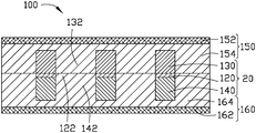
- FIG. 15 illustrates a printed circuit board with high-capacity copper circuit 100 according to a first exemplary embodiment.
- the printed circuit board with high-capacity copper circuit 100 includes a conductive trace 20 , a first protecting layer 150 , and a second protecting layer 160 .
- the first protecting layer 150 and the second protecting layer 160 are formed on opposite sides of the conductive trace 20 .
- the conductive trace 20 includes a base conductive trace pattern 120 , a first conductive trace pattern 130 , and a second conductive trace pattern 140 .
- the base conductive trace pattern 120 is sandwiched between the first conductive trace pattern 130 and the second conductive trace pattern 140 .
- the first conductive trace pattern 130 and the second conductive trace pattern 140 are directly formed on opposite surfaces of the base copper conductive trace pattern 120 by using a copper plating method, for example.
- the first conductive trace pattern 130 and the second conductive trace pattern 140 are in electrically contact with the base conductive trace pattern 120 .
- a line width of the base conductive trace pattern 120 , a line width of the first conductive trace pattern 130 , and a line width of the second conductive trace pattern 140 are substantially the same.
- a thickness of the first conductive trace pattern 130 is equal to a thickness of the second conductive trace pattern 140 .
- a thickness of the first conductive trace pattern 130 and a thickness of the second conductive trace pattern 140 are in a range from about 60 to 70 microns (i.e., 60 to 70*10 ⁇ circumflex over ( ) ⁇ -6 meters).
- the first protecting layer 150 covers the first conductive trace pattern 130 , and fills in the first gaps 132 between the first conductive trace pattern 130 .
- the second protecting layer 160 covers the second conductive trace pattern 140 , and fills in the second gaps 142 between the second conductive trace pattern 140 and the third gaps 122 between the base conductive trace pattern 120 .
- the first protecting layer 150 is a Cover Layer (CVL), and includes a base layer 152 and an adhering layer 154 formed on the base layer 152 .
- CVL Cover Layer
- FIG. 16 illustrates a flowchart of a manufacturing method in accordance with a second exemplary embodiment.
- An exemplary method 200 for manufacturing the thick copper circuit 100 (shown in FIG. 15 ) is provided by way of an example, as there are a variety of ways to carry out the method. Additionally, the illustrated order of blocks is by way of example only. The order of the blocks may change.
- the method 200 can begin at block 201 , as shown in FIG. 16 .
- a copper cladding substrate 10 is provided.
- the single side copper cladding substrate 10 includes a supporting sheet 11 and a base copper foil 12 .
- the base copper foil 12 includes a first surface 121 and a second surface 123 opposite to the first surface 121 .
- the supporting sheet 11 is located on the second surface 123 .
- the supporting sheet 11 is selected from a group consisting of polyethylene glycol terephthalate (PET), poly naphthalene dicarboxylic acid glycol ester (PEN), and polyimide (PI).
- a method of providing the single side copper cladding substrate 10 includes the following steps. First, as shown in FIG. 1 , a roll (roll 101 ) of flexible base copper foil 12 is provided and the base copper foil 12 is unrolled. The thickness of the base copper foil 12 is about 18 micrometers.
- the base copper foil 12 includes the first surface 121 and the second surface 123 opposite to the first surface 121 . Second, the supporting sheet 11 is laminated to the second surface 123 , and the base copper foil 12 adhering to the supporting sheet 11 is cut to a required size, thereby forming a plurality of pieces of the single side copper cladding substrate 10 .
- the supporting sheet 11 is provided from a wrapped roll and the supporting sheet 11 is unrolled.
- a copper plating method, or a copper deposition method or a sputtering process can then be used to form the base copper foil 12 on the supporting sheet 11 , creating a single side copper cladding substrate 10 .
- a first conductive trace pattern 130 is formed on the first surface 121 by using a copper electroplating method, for example.
- a first conductive circuit pattern is formed on a first surface of the base copper foil 12 .
- a method for forming the first conductive trace pattern 130 is as follows:
- a photosensitive film 110 is adhered to the first surface 121 , a thickness of the photosensitive film 110 is about 75 microns.
- the photosensitive film 110 is exposed, developed, and etched. As a result, a first shielding layer 112 is formed on the first surface 121 .
- the first shielding layer 112 includes a plurality of openings 114 .
- the openings 114 expose portions of the base copper foil 12 .
- a copper layer is formed in the openings 114 by using a electroplating method, for example.
- the plated copper layer forms the first conductive trace pattern 130 .
- the first shielding layer 112 is removed from the first surface 121 .
- the first conductive trace pattern 130 is situated on the surface 121 of the base copper foil 12 .
- a first protecting layer 150 is applied on the first conductive trace pattern 130 .
- the first protecting layer 150 protects the first conductive trace pattern 130 from oxidation, scratches, and so on.
- the first protecting layer 150 is CoverLay (CVL), and includes a base layer 152 and an adhering layer 154 formed on the base layer 152 .
- the adhering layer 154 fills in the first gaps 132 formed by the base copper foil 12 and the first conductive trace pattern 130 , and covers the first conductive trace pattern 130 .
- the first protecting layer 150 is a solder mask.
- the supporting sheet 11 (as shown in FIG. 7 ) is removed from the base copper foil 12 , and thickness of the base copper foil 12 is reduced by using a gridding method, for example. A thickness of the base copper foil 12 is reduced. The second surface 123 is removed by grinding, resulting in a third surface 125 . In this way, a thickness of the base copper foil 12 is retained to be about 2 to 6 microns.
- a second conductive trace pattern 140 is formed on the third surface 125 .
- the shape of the second conductive trace pattern 140 is the same as the shape of the first conductive trace pattern 130 , and a thickness of the second conductive trace pattern 140 is substantially equal to a thickness of the first conductive trace pattern 130 .
- the second conductive trace pattern 140 is formed using the same method as that used for the first conductive trace pattern 130 . That is to say, the second conductive trace pattern 140 is formed in the following way.
- a photosensitive film 115 is laminated to the third surface 125 .
- the photosensitive film 115 is exposed, developed, and etched to form a second shielding layer 116 on the third surface 125 , as shown in FIG. 11 .
- the second shielding layer 116 includes a plurality of openings 118 , the openings 118 are configured to expose portions of the base copper foil 12 .
- a copper layer is formed in the openings 118 by using an electroplating method, for example.
- the plating copper layer is configured to form the second conductive trace pattern 140 .
- the second shielding layer 116 is removed from the base copper foil 12 , the second conductive trace pattern 140 being on the third surface 125 .
- the respective thicknesses of the first conductive trace pattern 130 and of the second conductive trace pattern 140 are in a range from about 60 to 70 microns.
- the base copper foil 12 exposed in parts by the third gaps 122 is removed by etching
- the remaining portions of the base copper foil 12 form a base conductive trace pattern 120
- a thickness of the base conductive trace pattern is about 2-6 microns, in a preferred embodiment, a thickness of the base conductive trace pattern is about 2 microns.
- the third gaps 122 between the base conductive trace pattern 120 , the first gaps 132 between the first conductive trace pattern 130 , and the second gaps 142 between the second conductive trace pattern 140 are aligned with each other.
- the widths of the traces of the base conductive trace pattern 120 , of the first conductive trace pattern 130 , and of the second conductive trace pattern 140 are substantially the same.
- the base conductive trace pattern 120 , the first conductive trace pattern 130 , and the second conductive trace pattern 140 together form the conductive trace 20 .
- a thickness of the conductive trace 20 is about 122 microns to 146 microns. In a preferred embodiment, a thickness of the conductive trace 20 is about 125 microns.
- a width of each of the first gaps 132 of the first conductive trace pattern 130 is about 100 um or 130 um.
- a second protecting layer 160 is applied on the second conductive trace pattern 140 .
- the second protecting layer 160 also fills in the second gaps 142 between the second conductive trace pattern 140 , and the third gaps 122 between the base conductive trace pattern 120 .
- the circuit conductive 20 is formed by using an etching method and an electroplating method, for example. A thickness of the conductive trace 20 is about 125 microns. Thereby, the printed circuit board with thick copper circuit 100 is obtained.
- openings are formed in the first protective layer 150 and second protection layer 160 by a laser cutting method, and parts of the conductive trace 20 are exposed.
- the exposed portions can be used as electrical pads, and electronic components can be arranged on such pads.
Abstract
Description
Claims (11)
Priority Applications (1)
| Application Number | Priority Date | Filing Date | Title |
|---|---|---|---|
| US15/870,865 US11160166B2 (en) | 2016-10-06 | 2018-01-13 | Printed circuit board with high-capacity copper circuit |
Applications Claiming Priority (4)
| Application Number | Priority Date | Filing Date | Title |
|---|---|---|---|
| CN201610880403.9 | 2016-10-06 | ||
| CN201610880403.9A CN107920415B (en) | 2016-10-06 | 2016-10-06 | Circuit board with thick copper circuit and manufacturing method thereof |
| US15/394,735 US9907167B1 (en) | 2016-10-06 | 2016-12-29 | Method for manufacturing a printed circuit board with high-capacity copper circuit |
| US15/870,865 US11160166B2 (en) | 2016-10-06 | 2018-01-13 | Printed circuit board with high-capacity copper circuit |
Related Parent Applications (1)
| Application Number | Title | Priority Date | Filing Date |
|---|---|---|---|
| US15/394,735 Division US9907167B1 (en) | 2016-10-06 | 2016-12-29 | Method for manufacturing a printed circuit board with high-capacity copper circuit |
Publications (2)
| Publication Number | Publication Date |
|---|---|
| US20180139842A1 US20180139842A1 (en) | 2018-05-17 |
| US11160166B2 true US11160166B2 (en) | 2021-10-26 |
Family
ID=61225926
Family Applications (2)
| Application Number | Title | Priority Date | Filing Date |
|---|---|---|---|
| US15/394,735 Active US9907167B1 (en) | 2016-10-06 | 2016-12-29 | Method for manufacturing a printed circuit board with high-capacity copper circuit |
| US15/870,865 Active 2038-01-15 US11160166B2 (en) | 2016-10-06 | 2018-01-13 | Printed circuit board with high-capacity copper circuit |
Family Applications Before (1)
| Application Number | Title | Priority Date | Filing Date |
|---|---|---|---|
| US15/394,735 Active US9907167B1 (en) | 2016-10-06 | 2016-12-29 | Method for manufacturing a printed circuit board with high-capacity copper circuit |
Country Status (3)
| Country | Link |
|---|---|
| US (2) | US9907167B1 (en) |
| CN (1) | CN107920415B (en) |
| TW (1) | TWI640234B (en) |
Cited By (1)
| Publication number | Priority date | Publication date | Assignee | Title |
|---|---|---|---|---|
| US11582872B2 (en) * | 2017-04-28 | 2023-02-14 | Avary Holding (Shenzhen) Co., Limited. | Circuit board |
Families Citing this family (7)
| Publication number | Priority date | Publication date | Assignee | Title |
|---|---|---|---|---|
| CN109246925B (en) | 2018-08-28 | 2020-03-31 | 庆鼎精密电子(淮安)有限公司 | Manufacturing method of soft and hard board |
| CN110248465B (en) * | 2019-06-20 | 2024-03-19 | 上海铠琪科技有限公司 | Thick film and copper-clad integrated ceramic circuit board and preparation method thereof |
| CN110473836B (en) * | 2019-08-29 | 2021-01-05 | 丰鹏创科科技(珠海)有限公司 | Heat dissipation substrate, power device module and method for preparing heat dissipation substrate |
| CN110843702A (en) * | 2019-10-31 | 2020-02-28 | 武汉嘉晨汽车技术有限公司 | Novel PDU structure |
| KR20220086924A (en) * | 2020-12-17 | 2022-06-24 | 삼성전기주식회사 | Printed circuit board |
| KR20220091831A (en) * | 2020-12-24 | 2022-07-01 | 삼성전기주식회사 | Printed circuit board |
| KR20220098997A (en) * | 2021-01-05 | 2022-07-12 | 삼성전기주식회사 | Printed circuit board |
Citations (11)
| Publication number | Priority date | Publication date | Assignee | Title |
|---|---|---|---|---|
| US3791858A (en) * | 1971-12-13 | 1974-02-12 | Ibm | Method of forming multi-layer circuit panels |
| US5338900A (en) * | 1991-03-06 | 1994-08-16 | International Business Machines Corporation | Structures for electrically conductive decals filled with inorganic insulator material |
| TWM299436U (en) | 2006-04-27 | 2006-10-11 | Thinflex Corp | Hot rolling lamination apparatus |
| US20070268675A1 (en) * | 2006-05-22 | 2007-11-22 | Hitachi Cable Ltd. | Electronic device substrate, electronic device and methods for fabricating the same |
| US20110155439A1 (en) * | 2009-12-24 | 2011-06-30 | Shinko Electric Industries Co., Ltd. | Multilayer wiring substrate and method of manufacturing the same |
| US20110154657A1 (en) * | 2009-12-29 | 2011-06-30 | Subtron Technology Co. Ltd. | Manufacturing method of package carrier |
| CN102196668A (en) | 2010-03-08 | 2011-09-21 | 宏恒胜电子科技(淮安)有限公司 | Method for manufacturing circuit board |
| TW201134322A (en) | 2010-03-18 | 2011-10-01 | Foxconn Advanced Tech Inc | Method for manufacturing printed circuit board |
| US20150245484A1 (en) * | 2014-02-21 | 2015-08-27 | Samsung Electro-Mechanics Co., Ltd. | Printed circuit board and method of manufacturing the same |
| US20150351219A1 (en) * | 2011-04-15 | 2015-12-03 | Samsung Electro-Mechanics Co., Ltd. | Printed circuit board and method of manufacturing the same |
| US9832866B2 (en) * | 2015-06-29 | 2017-11-28 | Samsung Electro-Mechanics Co., Ltd. | Multilayered substrate and method of manufacturing the same |
Family Cites Families (4)
| Publication number | Priority date | Publication date | Assignee | Title |
|---|---|---|---|---|
| FI88241C (en) * | 1990-10-30 | 1993-04-13 | Nokia Mobile Phones Ltd | FOERFARANDE FOER FRAMSTAELLNING AV KRETSKORT |
| JP2003133719A (en) * | 2001-10-26 | 2003-05-09 | Sumitomo Bakelite Co Ltd | Manufacturing method of multilayer interconnection board |
| JP4713131B2 (en) * | 2004-11-19 | 2011-06-29 | 株式会社マルチ | Printed wiring board and method for manufacturing the printed wiring board |
| CN103687339B (en) * | 2012-09-26 | 2017-03-01 | 碁鼎科技秦皇岛有限公司 | Circuit board and preparation method thereof |
-
2016
- 2016-10-06 CN CN201610880403.9A patent/CN107920415B/en active Active
- 2016-11-21 TW TW105138076A patent/TWI640234B/en active
- 2016-12-29 US US15/394,735 patent/US9907167B1/en active Active
-
2018
- 2018-01-13 US US15/870,865 patent/US11160166B2/en active Active
Patent Citations (12)
| Publication number | Priority date | Publication date | Assignee | Title |
|---|---|---|---|---|
| US3791858A (en) * | 1971-12-13 | 1974-02-12 | Ibm | Method of forming multi-layer circuit panels |
| US5338900A (en) * | 1991-03-06 | 1994-08-16 | International Business Machines Corporation | Structures for electrically conductive decals filled with inorganic insulator material |
| TWM299436U (en) | 2006-04-27 | 2006-10-11 | Thinflex Corp | Hot rolling lamination apparatus |
| US20070268675A1 (en) * | 2006-05-22 | 2007-11-22 | Hitachi Cable Ltd. | Electronic device substrate, electronic device and methods for fabricating the same |
| US20110155439A1 (en) * | 2009-12-24 | 2011-06-30 | Shinko Electric Industries Co., Ltd. | Multilayer wiring substrate and method of manufacturing the same |
| US20110154657A1 (en) * | 2009-12-29 | 2011-06-30 | Subtron Technology Co. Ltd. | Manufacturing method of package carrier |
| CN102196668A (en) | 2010-03-08 | 2011-09-21 | 宏恒胜电子科技(淮安)有限公司 | Method for manufacturing circuit board |
| US8377317B2 (en) | 2010-03-08 | 2013-02-19 | Hong Heng Sheng Electrical Technology (HuaiAn) Co., Ltd | Method for manufacturing printed circuit board with thick traces |
| TW201134322A (en) | 2010-03-18 | 2011-10-01 | Foxconn Advanced Tech Inc | Method for manufacturing printed circuit board |
| US20150351219A1 (en) * | 2011-04-15 | 2015-12-03 | Samsung Electro-Mechanics Co., Ltd. | Printed circuit board and method of manufacturing the same |
| US20150245484A1 (en) * | 2014-02-21 | 2015-08-27 | Samsung Electro-Mechanics Co., Ltd. | Printed circuit board and method of manufacturing the same |
| US9832866B2 (en) * | 2015-06-29 | 2017-11-28 | Samsung Electro-Mechanics Co., Ltd. | Multilayered substrate and method of manufacturing the same |
Cited By (1)
| Publication number | Priority date | Publication date | Assignee | Title |
|---|---|---|---|---|
| US11582872B2 (en) * | 2017-04-28 | 2023-02-14 | Avary Holding (Shenzhen) Co., Limited. | Circuit board |
Also Published As
| Publication number | Publication date |
|---|---|
| TW201815242A (en) | 2018-04-16 |
| TWI640234B (en) | 2018-11-01 |
| CN107920415B (en) | 2020-11-03 |
| CN107920415A (en) | 2018-04-17 |
| US9907167B1 (en) | 2018-02-27 |
| US20180139842A1 (en) | 2018-05-17 |
Similar Documents
| Publication | Publication Date | Title |
|---|---|---|
| US11160166B2 (en) | Printed circuit board with high-capacity copper circuit | |
| US10674610B1 (en) | Multilayer rigid flexible printed circuit board and method for manufacturing the same | |
| US9277640B2 (en) | Flexible printed circuit board and method for manufacturing same | |
| CN106664800B (en) | Printed circuit board, electronic component and the method for making printed circuit board | |
| US7987586B2 (en) | Method for manufacturing printed circuit board having different thicknesses in different areas | |
| US10117328B1 (en) | Flexible circuit board and method for manufacturing same | |
| US20130341073A1 (en) | Packaging substrate and method for manufacturing same | |
| US20130118009A1 (en) | Method for manufacturing printed circuit board | |
| US8377317B2 (en) | Method for manufacturing printed circuit board with thick traces | |
| KR20130064044A (en) | Printed substrate manufacturing method and printed substrate employing same | |
| US9622340B2 (en) | Flexible circuit board and method for manufacturing same | |
| US20030207211A1 (en) | Process for massively producing tape type flexible printed circuits | |
| CN108124386A (en) | Wiring board and its production method, graph transfer method | |
| US20130220683A1 (en) | Printed circuit board and method for manufacturing printed circuit board | |
| US8280204B2 (en) | Optical wiring board and manufacturing method thereof | |
| CN216217750U (en) | Electroplating type stepped welding pad PCB | |
| KR20020050720A (en) | Processes for manufacturing multilayer flexible wiring boards | |
| KR102138341B1 (en) | Film type antenna using high ductility nickel/stannum plating and its manufacturing method | |
| US11665831B2 (en) | Method for manufacturing a circuit board with embedded nickel resistor | |
| US11582872B2 (en) | Circuit board | |
| CN110876239B (en) | Circuit board and manufacturing method thereof | |
| CN111447745A (en) | Preparation method of embedded circuit board | |
| JP4123637B2 (en) | Film carrier manufacturing method | |
| CN103841753A (en) | Printed circuit board and manufacturing method thereof | |
| JP4385482B2 (en) | Film carrier manufacturing method |
Legal Events
| Date | Code | Title | Description |
|---|---|---|---|
| AS | Assignment |
Owner name: HONGQISHENG PRECISION ELECTRONICS (QINHUANGDAO) CO.,LTD., CHINA Free format text: ASSIGNMENT OF ASSIGNORS INTEREST;ASSIGNORS:XU, FANG-BO;WU, PENG;SHEN, JIAN-QUAN;AND OTHERS;REEL/FRAME:044615/0103 Effective date: 20180110 Owner name: HONGQISHENG PRECISION ELECTRONICS (QINHUANGDAO) CO Free format text: ASSIGNMENT OF ASSIGNORS INTEREST;ASSIGNORS:XU, FANG-BO;WU, PENG;SHEN, JIAN-QUAN;AND OTHERS;REEL/FRAME:044615/0103 Effective date: 20180110 Owner name: AVARY HOLDING (SHENZHEN) CO., LIMITED., CHINA Free format text: ASSIGNMENT OF ASSIGNORS INTEREST;ASSIGNORS:XU, FANG-BO;WU, PENG;SHEN, JIAN-QUAN;AND OTHERS;REEL/FRAME:044615/0103 Effective date: 20180110 |
|
| FEPP | Fee payment procedure |
Free format text: ENTITY STATUS SET TO UNDISCOUNTED (ORIGINAL EVENT CODE: BIG.); ENTITY STATUS OF PATENT OWNER: LARGE ENTITY |
|
| STPP | Information on status: patent application and granting procedure in general |
Free format text: DOCKETED NEW CASE - READY FOR EXAMINATION |
|
| STPP | Information on status: patent application and granting procedure in general |
Free format text: NON FINAL ACTION MAILED |
|
| STPP | Information on status: patent application and granting procedure in general |
Free format text: FINAL REJECTION MAILED |
|
| STPP | Information on status: patent application and granting procedure in general |
Free format text: DOCKETED NEW CASE - READY FOR EXAMINATION |
|
| STPP | Information on status: patent application and granting procedure in general |
Free format text: NON FINAL ACTION MAILED |
|
| STPP | Information on status: patent application and granting procedure in general |
Free format text: RESPONSE TO NON-FINAL OFFICE ACTION ENTERED AND FORWARDED TO EXAMINER |
|
| STPP | Information on status: patent application and granting procedure in general |
Free format text: NOTICE OF ALLOWANCE MAILED -- APPLICATION RECEIVED IN OFFICE OF PUBLICATIONS |
|
| STPP | Information on status: patent application and granting procedure in general |
Free format text: PUBLICATIONS -- ISSUE FEE PAYMENT VERIFIED |
|
| STCF | Information on status: patent grant |
Free format text: PATENTED CASE |