US11158357B2 - Method of performing internal processing operations with pre-defined protocol interface of memory device - Google Patents

Method of performing internal processing operations with pre-defined protocol interface of memory device Download PDF

Info

Publication number
US11158357B2
US11158357B2 US16/813,851 US202016813851A US11158357B2 US 11158357 B2 US11158357 B2 US 11158357B2 US 202016813851 A US202016813851 A US 202016813851A US 11158357 B2 US11158357 B2 US 11158357B2
Authority
US
United States
Prior art keywords
memory
pim
internal processing
command
memory device
Prior art date
Legal status (The legal status is an assumption and is not a legal conclusion. Google has not performed a legal analysis and makes no representation as to the accuracy of the status listed.)
Active
Application number
US16/813,851
Other versions
US20200294558A1 (en
Inventor
Hak-soo Yu
Namsung KIM
Kyomin SOHN
Seongil O
Sukhan Lee
Current Assignee (The listed assignees may be inaccurate. Google has not performed a legal analysis and makes no representation or warranty as to the accuracy of the list.)
Samsung Electronics Co Ltd
Original Assignee
Samsung Electronics Co Ltd
Priority date (The priority date is an assumption and is not a legal conclusion. Google has not performed a legal analysis and makes no representation as to the accuracy of the date listed.)
Filing date
Publication date
Priority claimed from KR1020190161673A external-priority patent/KR20200108772A/en
Application filed by Samsung Electronics Co Ltd filed Critical Samsung Electronics Co Ltd
Priority to US16/813,851 priority Critical patent/US11158357B2/en
Assigned to SAMSUNG ELECTRONICS CO., LTD. reassignment SAMSUNG ELECTRONICS CO., LTD. ASSIGNMENT OF ASSIGNORS INTEREST (SEE DOCUMENT FOR DETAILS). Assignors: KIM, NAMSUNG, LEE, SUKHAN, O, SEONGIL, SOHN, KYOMIN, YU, HAK-SOO
Publication of US20200294558A1 publication Critical patent/US20200294558A1/en
Priority to US17/504,918 priority patent/US20220036929A1/en
Application granted granted Critical
Publication of US11158357B2 publication Critical patent/US11158357B2/en
Active legal-status Critical Current
Anticipated expiration legal-status Critical

Links

Images

Classifications

    • GPHYSICS
    • G06COMPUTING; CALCULATING OR COUNTING
    • G06FELECTRIC DIGITAL DATA PROCESSING
    • G06F3/00Input arrangements for transferring data to be processed into a form capable of being handled by the computer; Output arrangements for transferring data from processing unit to output unit, e.g. interface arrangements
    • G06F3/06Digital input from, or digital output to, record carriers, e.g. RAID, emulated record carriers or networked record carriers
    • G06F3/0601Interfaces specially adapted for storage systems
    • G06F3/0628Interfaces specially adapted for storage systems making use of a particular technique
    • G06F3/0629Configuration or reconfiguration of storage systems
    • GPHYSICS
    • G11INFORMATION STORAGE
    • G11CSTATIC STORES
    • G11C7/00Arrangements for writing information into, or reading information out from, a digital store
    • G11C7/10Input/output [I/O] data interface arrangements, e.g. I/O data control circuits, I/O data buffers
    • G11C7/1015Read-write modes for single port memories, i.e. having either a random port or a serial port
    • G11C7/1045Read-write mode select circuits
    • GPHYSICS
    • G06COMPUTING; CALCULATING OR COUNTING
    • G06FELECTRIC DIGITAL DATA PROCESSING
    • G06F13/00Interconnection of, or transfer of information or other signals between, memories, input/output devices or central processing units
    • G06F13/14Handling requests for interconnection or transfer
    • G06F13/16Handling requests for interconnection or transfer for access to memory bus
    • G06F13/1668Details of memory controller
    • GPHYSICS
    • G06COMPUTING; CALCULATING OR COUNTING
    • G06FELECTRIC DIGITAL DATA PROCESSING
    • G06F3/00Input arrangements for transferring data to be processed into a form capable of being handled by the computer; Output arrangements for transferring data from processing unit to output unit, e.g. interface arrangements
    • G06F3/06Digital input from, or digital output to, record carriers, e.g. RAID, emulated record carriers or networked record carriers
    • G06F3/0601Interfaces specially adapted for storage systems
    • G06F3/0602Interfaces specially adapted for storage systems specifically adapted to achieve a particular effect
    • G06F3/0625Power saving in storage systems
    • GPHYSICS
    • G11INFORMATION STORAGE
    • G11CSTATIC STORES
    • G11C11/00Digital stores characterised by the use of particular electric or magnetic storage elements; Storage elements therefor
    • G11C11/21Digital stores characterised by the use of particular electric or magnetic storage elements; Storage elements therefor using electric elements
    • G11C11/34Digital stores characterised by the use of particular electric or magnetic storage elements; Storage elements therefor using electric elements using semiconductor devices
    • G11C11/40Digital stores characterised by the use of particular electric or magnetic storage elements; Storage elements therefor using electric elements using semiconductor devices using transistors
    • G11C11/401Digital stores characterised by the use of particular electric or magnetic storage elements; Storage elements therefor using electric elements using semiconductor devices using transistors forming cells needing refreshing or charge regeneration, i.e. dynamic cells
    • G11C11/4063Auxiliary circuits, e.g. for addressing, decoding, driving, writing, sensing or timing
    • G11C11/407Auxiliary circuits, e.g. for addressing, decoding, driving, writing, sensing or timing for memory cells of the field-effect type
    • G11C11/408Address circuits
    • G11C11/4087Address decoders, e.g. bit - or word line decoders; Multiple line decoders
    • GPHYSICS
    • G11INFORMATION STORAGE
    • G11CSTATIC STORES
    • G11C11/00Digital stores characterised by the use of particular electric or magnetic storage elements; Storage elements therefor
    • G11C11/21Digital stores characterised by the use of particular electric or magnetic storage elements; Storage elements therefor using electric elements
    • G11C11/34Digital stores characterised by the use of particular electric or magnetic storage elements; Storage elements therefor using electric elements using semiconductor devices
    • G11C11/40Digital stores characterised by the use of particular electric or magnetic storage elements; Storage elements therefor using electric elements using semiconductor devices using transistors
    • G11C11/401Digital stores characterised by the use of particular electric or magnetic storage elements; Storage elements therefor using electric elements using semiconductor devices using transistors forming cells needing refreshing or charge regeneration, i.e. dynamic cells
    • G11C11/4063Auxiliary circuits, e.g. for addressing, decoding, driving, writing, sensing or timing
    • G11C11/407Auxiliary circuits, e.g. for addressing, decoding, driving, writing, sensing or timing for memory cells of the field-effect type
    • G11C11/409Read-write [R-W] circuits 
    • GPHYSICS
    • G11INFORMATION STORAGE
    • G11CSTATIC STORES
    • G11C5/00Details of stores covered by group G11C11/00
    • G11C5/02Disposition of storage elements, e.g. in the form of a matrix array
    • G11C5/025Geometric lay-out considerations of storage- and peripheral-blocks in a semiconductor storage device
    • GPHYSICS
    • G11INFORMATION STORAGE
    • G11CSTATIC STORES
    • G11C5/00Details of stores covered by group G11C11/00
    • G11C5/06Arrangements for interconnecting storage elements electrically, e.g. by wiring
    • G11C5/063Voltage and signal distribution in integrated semi-conductor memory access lines, e.g. word-line, bit-line, cross-over resistance, propagation delay
    • GPHYSICS
    • G11INFORMATION STORAGE
    • G11CSTATIC STORES
    • G11C7/00Arrangements for writing information into, or reading information out from, a digital store
    • G11C7/10Input/output [I/O] data interface arrangements, e.g. I/O data control circuits, I/O data buffers
    • G11C7/1006Data managing, e.g. manipulating data before writing or reading out, data bus switches or control circuits therefor
    • GPHYSICS
    • G11INFORMATION STORAGE
    • G11CSTATIC STORES
    • G11C7/00Arrangements for writing information into, or reading information out from, a digital store
    • G11C7/10Input/output [I/O] data interface arrangements, e.g. I/O data control circuits, I/O data buffers
    • G11C7/1015Read-write modes for single port memories, i.e. having either a random port or a serial port
    • G11C7/1039Read-write modes for single port memories, i.e. having either a random port or a serial port using pipelining techniques, i.e. using latches between functional memory parts, e.g. row/column decoders, I/O buffers, sense amplifiers
    • GPHYSICS
    • G11INFORMATION STORAGE
    • G11CSTATIC STORES
    • G11C7/00Arrangements for writing information into, or reading information out from, a digital store
    • G11C7/10Input/output [I/O] data interface arrangements, e.g. I/O data control circuits, I/O data buffers
    • G11C7/1078Data input circuits, e.g. write amplifiers, data input buffers, data input registers, data input level conversion circuits
    • G11C7/109Control signal input circuits
    • GPHYSICS
    • G11INFORMATION STORAGE
    • G11CSTATIC STORES
    • G11C8/00Arrangements for selecting an address in a digital store
    • G11C8/12Group selection circuits, e.g. for memory block selection, chip selection, array selection

Definitions

  • the inventive concept relates to apparatuses and methods, and more particularly, to a memory device that performs an internal processing operation by using a pre-defined protocol interface, a method of operating the memory device, and a memory system including the memory device.
  • a personal-in-memory (PIM) type processor may be located within a memory device to perform some computational operations of a computing system as internal processing. Through the internal processing of the memory device, the computational operation load of the computing system may be reduced.
  • PIM personal-in-memory
  • At least one exemplary embodiment of the inventive concept provides a memory device for performing an internal processing operation by using a pre-defined protocol interface, a method of operating the memory device, and a memory system including the memory device.
  • a memory device including a memory cell array including a first memory region and a second memory region; signal lines (e.g., command/address signal lines) configured to receive a command and an address from a source located outside the memory device; mode selector circuit configured to generate a processing mode selection signal for controlling the memory device to enter an internal processing mode based on the address received together with the command; a command converter circuit configured to convert the received command into an internal processing operation command in response to activation of the internal processing mode selection signal; and an internal processor configured to perform an internal processing operation on the first memory region in response to the internal processing operation command, in the internal processing mode.
  • signal lines e.g., command/address signal lines
  • mode selector circuit configured to generate a processing mode selection signal for controlling the memory device to enter an internal processing mode based on the address received together with the command
  • a command converter circuit configured to convert the received command into an internal processing operation command in response to activation of the internal processing mode selection signal
  • an internal processor configured to perform an internal processing operation on the first memory
  • a method of operating a memory device including a memory cell array including a first memory region and a second memory region, and an internal processor configured to perform an internal processing operation, the method including receiving a command and an address from a source located outside the memory device through a pre-defined protocol interface; generating a processing mode selection signal for controlling the memory device to enter an internal processing mode based on the address received together with the command; converting the received command into an internal processing operation command in response to activation of the internal processing mode selection signal; and the internal processor performing an internal processing operation on the first memory region in response to the internal processing operation command, in the internal processing mode.
  • a memory system including a memory device; and a memory controller configured to control the memory device by using a pre-defined protocol interface connected to the memory device.
  • the memory device includes a memory cell array including a first memory region and a second memory region; an mode selector circuit configured to receive a command and an address from the memory controller through the pre-defined protocol interface and, based on the address received together with the command, generate a processing mode selection signal for controlling the memory device to enter an internal processing mode; a command converter circuit configured to convert the received command into an internal processing operation command in response to activation of the internal processing mode selection signal; and an internal processor configured to perform an internal processing operation on the first memory region in response to the internal processing operation command, in the internal processing mode.
  • FIG. 1 is a diagram showing a system including a memory device that performs an internal processing operation according to an exemplary embodiment of the inventive concept
  • FIG. 2 is a block diagram for describing a memory device according to an exemplary embodiment of the inventive concept
  • FIGS. 3 to 5 are diagrams for describing a portion of a structure of the memory device of FIG. 2 ;
  • FIG. 6 is a flowchart for describing an operation of the memory device of FIG. 2 according to an exemplary embodiment of the inventive concept
  • FIG. 7 is a timing diagram for describing an operation of a memory device of FIG. 2 according to an exemplary embodiment of the inventive concept
  • FIG. 8 is a diagram for describing a PIM mode selector of FIG. 2 according to an exemplary embodiment of the inventive concept.
  • FIG. 9 is a flowchart for describing an operation of the memory device of FIG. 2 according to an exemplary embodiment of the inventive concept.
  • FIG. 1 is a diagram showing a system including a memory device that performs an internal processing operation according to exemplary embodiment of the inventive concept.
  • a system 100 includes a host device 110 and a memory device 120 .
  • the host device 110 may be communicatively connected to the memory device 120 via a memory bus 130 .
  • connections and/or “coupled” along with their derivatives. These terms are not necessarily intended as synonyms for each other. For example, descriptions using the terms “connected” and/or “coupled” may indicate that two or more elements are in direct physical or electrical contact with each other. In addition, the terms “connected” and/or “coupled” may also mean that two or more elements are not in direct contact with each other but still cooperate or interact with each other.
  • the host device 110 may be, for example, a computing system like a computer, a laptop computer, a server, a workstation, a portable communication terminal, a personal digital assistant (PDA), a portable multimedia player (PMP), a smart phone, or a wearable device.
  • the host device 110 may be one of a plurality of components included in a computing system, e.g., a graphics card.
  • the host device 110 is a functional block for performing general computer operations in the system 100 and may correspond to a central processing unit (CPU), a digital signal processor (DSP), a graphics processing unit (GPU), or an application processor (AP).
  • the host device 110 may include a memory controller 112 (e.g., a control circuit) that manages data transmission and reception to and from the memory device 120 .
  • the memory controller 112 may access the memory device 120 according to a memory request of the host device 110 .
  • the memory controller 112 includes a memory physical layer interface 114 for interfacing with the memory device 120 .
  • the memory controller 112 may be used for selecting rows and columns corresponding to memory locations, writing data to memory locations, or reading written data.
  • the memory physical layer interface 114 may be referred to as a memory PHY 114 .
  • the memory controller 112 includes a control register 116 .
  • the control register 116 may be used for initializing the memory device 120 and/or controlling the memory device 120 according to operating characteristics of the memory device 120 . After the system 100 is powered up, the memory controller 112 may set the control register 116 .
  • the control register 116 may store various codes configured to allow the memory controller 112 to normally interoperate with the memory device 120 . For example, codes indicating a frequency, a timing, and detailed operation parameters of the memory device 120 may be stored in the control register 116 . Also, the control register 116 may store specific address information used by the controller 112 to physically or logically divide a memory cell array 121 of the memory device 120 according to an operation mode.
  • the specific address information may indicate specific addresses used to divide the memory cell array 121 into a PIM region 122 and a normal memory region 124 .
  • the PIM region 122 may be a memory cell region accessed when the memory device 120 operates in an internal processing mode
  • the normal memory region may be a memory cell region accessed when the memory device 120 operates in a normal mode.
  • a specific address may indicate an address used to access the PIM region 122 and may serve as a basic signal for allowing the memory device 120 to enter the internal processing mode.
  • a specific address may include, for example, a stack identification signal, a channel address, or a bank address.
  • the specific address may include a combination of a stack identification signal, a channel address, and/or a bank address.
  • the memory controller 112 may control a write operation or a read operation for the memory device 120 by providing a command CMD (e.g., a read command, a write command, a verify command, etc.) and an address ADDR to the memory device 120 .
  • a command CMD e.g., a read command, a write command, a verify command, etc.
  • data DQ to be written and read data DQ may be transmitted and received between the memory controller 112 and the memory device 120 .
  • the data DQ may be transmitted from the memory controller 112 to the memory device 120 , the memory device 120 may receive the transmitted data DQ, and then the memory device 120 may write the received data DQ to the memory cell array 121 during a first memory access operation.
  • the memory device 120 may read the data DQ from the memory cell array 121 , the memory device 120 may transmit the read data DQ to the memory controller 112 , and then the memory controller 112 may receive the transmitted data DQ during a second memory access operation. Such a memory access operation may be performed through the memory PHY 114 and the memory bus 130 between the memory controller 112 and the memory device 120 .
  • the memory PHY 114 is a physical or electrical layer and a logical layer provided for signals, frequencies, timings, detailed operation parameters, and functionality needed for an efficient communication between the memory controller 112 and the memory device 120 .
  • the memory PHY 114 may support the features of a double data rate (DDR) protocol and/or a low power double data rate (LPDDR) protocol of the Joint Electron Device Engineering Council (JEDEC) standard.
  • DDR double data rate
  • LPDDR low power double data rate
  • JEDEC Joint Electron Device Engineering Council
  • the memory PHY 114 may include connectors for connecting the memory controller 110 and the memory device 120 .
  • the connectors may be implemented as pins, balls, signal lines, or other hardware components.
  • a clock signal CK FIG. 7
  • a command CMD FIG. 7
  • an address ADDR Address Dever Dever 114
  • data DQ Data DQ
  • Reuse of existing connectors in the memory PHY 114 may save significant space in an integrated circuit IC and avoid the cost for extending additional wires to the memory device 120 . Also, avoiding additional pins and wires eliminates potential electro-magnetic interference (EMI) due to the presence of additional wires and, since large numbers of drivers and receivers are not needed, power conservation may be realized.
  • EMI electro-magnetic interference
  • the memory bus 130 may include command/address signal lines 132 for transmitting command/address CMD/ADDR and data lines 134 for transmitting the data DQ.
  • command/address signal lines 132 and the data lines 134 are single lines between the memory controller 110 and the memory device 120 , but the command/address signal lines 132 and the data lines 134 may actually be a plurality of signal lines.
  • the memory device 120 may write data or read data under the control of the memory controller 112 .
  • the memory device 120 may be a DDR synchronous dynamic random access memory (SDRAM) device.
  • SDRAM synchronous dynamic random access memory
  • the inventive concept is not limited thereto, and the memory device 120 may be any one of volatile memory devices like an LPDDR SDRAM, a wide I/O DRAM, a high bandwidth memory (HBM), and a hybrid memory cube (HMC).
  • the memory device 120 may be any one of non-volatile memory devices like a flash memory, a phase-change RAM (PRAM), a magnetic RAM (MRAM), a resistive RAM (RRAM), and a ferroelectric RAM (FRAM).
  • PRAM phase-change RAM
  • MRAM magnetic RAM
  • RRAM resistive RAM
  • FRAM ferroelectric RAM
  • the memory device 120 operates in one of the normal mode and the internal processing mode.
  • the normal mode refers to an operation mode for performing a general data transaction operation
  • the internal processing mode refers to an operation mode for performing an internal processing operation.
  • a general data transaction operation is a data exchange operation performed according to a predefined protocol like the DDR protocol and/or the LPDDR protocol.
  • the memory device 120 performs an internal processing operation under the control of the memory controller 112 .
  • the memory controller 112 may provide a specific address, which is the basis of an internal processing operation to be performed by the memory device 120 , to the memory device 120 through the command/address signal lines 132 by using a predefined protocol like the DDR protocol and/or the LPDDR protocol.
  • the memory device 120 may enter the internal processing mode based on the specific address.
  • the specific address may be provided via an existing connector of the memory PHY 114 .
  • the specific address which is the basis of an internal processing operation, may be statically set when the memory device 120 is mounted in the system 100 .
  • Static setting means that the specific address may be fixed by using one specific address information.
  • the specific address is dynamically set before and after an internal processing operation of the memory device 120 .
  • the specific address may be changed by using various combinations of specific address information during a dynamic setting.
  • the memory device 120 includes the memory cell array 121 and a PIM command converter 126 (e.g., a processor or a logic circuit).
  • the memory cell array 121 includes the PIM region 122 and the normal memory region 124 that are physically or logically divided according to an operation mode of the memory device 120 .
  • the PIM region 122 may refer to a memory cell region configured to access internal processing data for an internal processing operation performed in the internal processing mode.
  • Internal processing operations of the memory device 120 may include a write operation to the PIM region 122 and/or a read operation from the PIM region 122 .
  • the normal memory region 124 may refer to a memory cell region configured to access data according to a general data transaction operation performed in the normal mode.
  • Data transaction operations of memory device 120 may include a write operation to the normal memory region 124 and/or a read operation from the normal memory region 124 .
  • the PIM command converter 126 converts the command CMD received through the command/address signal lines 132 into an internal processing operation command PIM_CMD.
  • the PIM command converter 126 may convert the command CMD received through the command/address signal lines 132 into the internal processing operation command PIM_CMD instructing a type of internal processing operation (e.g., data search, data arithmetic operation (e.g., add, subtract, multiple, divide, etc.), data move, data inversion, data shift, data swap, data comparison, logical operations, data processing/operations, etc.).
  • the internal processing operation command PIM_CMD may include an internal processing read command and/or an internal processing write command associated with an internal processing operation.
  • An internal processing operation for reading internal processing data from the PIM region 122 or writing internal processing data to the PIM region 122 may be performed according to the internal processing operation command PIM_CMD.
  • the internal processing data may refer to reference data or target data used in an internal processing operation.
  • the internal processing data may include address information related to an internal processing operation like a data swap.
  • FIG. 2 is a block diagram for describing a memory device according to an exemplary embodiment of the inventive concept.
  • the memory device 120 includes the memory cell array 121 including the PIM region 122 and the normal memory region 124 , the PIM command converter 126 , a PIM mode selector 210 (e.g., logic circuit), a first switch 231 , a second switch 232 , a PIM engine 250 (e.g., a processor or logic circuit), and a data input/output circuit 260 .
  • a PIM mode selector 210 e.g., logic circuit
  • a first switch 231 e.g., a second switch 232
  • a PIM engine 250 e.g., a processor or logic circuit
  • a data input/output circuit 260 e.g., a processor or logic circuit
  • the PIM region 122 may be a region defined to access (e.g., to store) and output internal processing data for an internal processing operation when the memory device 120 operates in the internal processing mode.
  • the normal memory region 124 may be a region defined to access data according to a general data transaction operation when the memory device 120 operates in the normal mode.
  • the PIM region 122 and the normal memory region 124 may be set as fixed regions in the memory cell array 121 . In an exemplary embodiment where the regions are fixed, their sizes and physical locations within the memory cell array 121 remain constant. According to embodiments, the PIM region 122 and the normal memory region 124 may be set as variable regions in the memory cell array 121 . In an exemplary embodiment where the regions are variable, their sizes and physical locations within the memory cell array 121 , their sizes and physical locations within the memory cell array 121 may dynamically change based on or more conditions.
  • the PIM command converter 126 may convert the command CMD received through the command/address signal lines 132 into the internal processing operation command PIM_CMD.
  • the PIM mode selector 210 may receive the address ADDR from the memory controller 112 through the command/address signal lines 132 of the memory bus 130 and output a PIM mode selection signal PIM_SEL in response to the received address ADDR.
  • the PIM mode selector 210 may determine whether a specific address is included in the received address ADDR and output the PIM mode selection signal PIM_SEL as a result of the determination.
  • the PIM mode selector 210 outputs a PIM mode selection signal PIM_SEL set to a first logic level to indicate the internal processing mode when the received address ADDR is within a predefined range of addresses and outputs the PIM mode selection signal PIM_SEL set to a second other logic level to indicate the normal mode when the received address ADDR is outside the predefined range of addresses.
  • the specific address may be an address within the range or the specific address itself.
  • the specific address that the PIM mode selector 210 is aware of is the same as a specific address that is stored in the control register 116 of the memory controller 112 and used to address the PIM region 122 .
  • one or more addresses may be stored in the control register 116 as the specific address.
  • the PIM mode selection signal PIM_SEL serves as a control signal for determining whether the memory device 120 is to enter and operate in the internal processing mode or the normal mode.
  • the specific address may alternately be stored outside the control register 116 within a memory of the memory controller 112 or within a memory of the host device 110 outside the memory controller.
  • the PIM mode selector 210 may activate the PIM mode selection signal PIM_SEL when a specific address is included in the address ADDR received through the command/address signal lines 132 . By activating the PIM mode selection signal PIM_SEL, the memory device 120 may operate in the internal processing mode.
  • the PIM mode selector 210 may deactivate the PIM mode selection signal PIM_SEL when no specific address is included in the address ADDR received through the command/address signal lines 132 .
  • the PIM mode selection signal PIM_SEL may be activated by setting it the first logic level and deactivated by setting it to the second logic level. By deactivating the PIM mode selection signal PIM_SEL, the memory device 120 may operate in the normal mode.
  • the PIM mode selection signal PIM_SEL may be provided to the first switch 231 and the second switch 232 .
  • the first switch 231 may selectively connect the command/address signal lines 132 to input signal lines 221 or internal command signal lines 240 of the PIM command converter 126 in response to the PIM mode selection signal PIM_SEL.
  • the second switch 232 may selectively connect output signal lines 222 or the internal command signal lines 240 of the PIM command converter 126 to the memory cell array 121 and the PIM engine 250 in response to the PIM mode selection signal PIM_SEL.
  • the first switch 231 may selectively connect the command/address signal lines 132 to the input signal lines 221 of the PIM command converter 126 in response to activation of the PIM mode selection signal PIM_SEL.
  • the first switch 231 may provide the command CMD received through the command/address signal lines 132 to the PIM command converter 126 .
  • the PIM command converter 126 may convert the command CMD received through the input signal lines 221 into the internal processing operation command PIM_CMD and output the internal processing operation command PIM_CMD to the output signal lines 222 .
  • the internal processing operation command PIM_CMD may be a command associated with an internal processing operation performed in the internal processing mode.
  • the second switch 232 may connect output signal lines 221 of the PIM command converter 126 to the memory cell array 121 and/or the PIM engine 250 in response to activation of the PIM mode selection signal PIM_SEL.
  • the second switch 232 may provide the internal processing operation command PIM_CMD output through the output signal lines 222 of the PIM command converter 126 to the PIM region 122 and/or the PIM engine 250 of the memory cell array 121 .
  • the PIM engine 250 may access the PIM region 122 according to the internal processing operation command PIM_CMD and perform an internal processing operation.
  • an internal processing operation may include a processing operation for internal processing data stored in the PIM region 122 , e.g., data search, data arithmetic operation (e.g., add, subtract, multiple, divide, etc.), data move, data inversion, data shift, data swap, data comparison, logical operations, data processing/operations, etc.
  • data search e.g., data search, data arithmetic operation (e.g., add, subtract, multiple, divide, etc.), data move, data inversion, data shift, data swap, data comparison, logical operations, data processing/operations, etc.
  • data arithmetic operation e.g., add, subtract, multiple, divide, etc.
  • data move e.g., data inversion, data shift, data swap, data comparison, logical operations, data processing/operations, etc.
  • the first switch 231 may connect the command/address signal lines 132 to the internal command signal lines 240 in response to deactivation of the PIM mode selection signal PIM_SEL and the command CMD received through the command/address signal lines 132 to the internal command signal lines 240 .
  • the command CMD provided to the internal command signal lines 240 may be a command associated with a data transaction operation performed in the normal mode.
  • the second switch 232 may connect the internal command signal lines 240 to the memory cell array 121 in response to deactivation of the PIM mode selection signal PIM_SEL.
  • the normal memory region 124 of the memory cell array 121 may be accessed according to the command CMD provided to the internal command signal lines 240 , and thus a data transaction operation may be performed.
  • the second switch 232 may connect the internal command signal lines 240 to the normal memory region 124 in response to deactivation of the PIM mode selection signal PIM_SEL.
  • the PIM engine 250 may perform an internal processing operation according to the internal processing operation command PIM_CMD.
  • the PIM engine 250 may perform an internal processing operation on internal processing data according to the internal processing operation command PIM_CMD by using the PIM region 122 of the memory cell array 121 .
  • the PIM engine 250 is hardware having processing functionality, similar to a processor (e.g., a CPU) included in the host device 110 .
  • a processor e.g., a CPU
  • the term “internal” means that the PIM engine 250 exists within the memory device 120 . Therefore, a processor existing “outside” the memory device 120 may refer to, for example, a processor of the host device 110 .
  • the data input/output circuit 260 may operate as a write driver (e.g., a driving circuit) or a sense amplifier of the memory device 120 .
  • the data input/output circuit 260 may receive the data DQ from the memory controller 112 through data lines 134 of the memory bus 130 and provide the received data DQ to the memory cell array 121 and/or the PIM engine 250 .
  • the data input/output circuit 260 may receive the data DQ from the memory cell array 121 and/or the PIM engine 250 and transmit the received data DQ to the memory controller 112 through the data lines 134 .
  • the PIM engine 250 may perform an internal processing operation.
  • the PIM engine 250 may transmit/receive the data DQ to/from the memory controller 112 through the data input/output circuit 260 and the data lines 134 .
  • the data DQ received through the data lines 134 and the data input/output circuit 260 may be stored in the PIM region 122 of the memory cell array 121 as internal processing data.
  • the PIM engine 250 may store internal processing data according to an internal processing operation performed in response to the internal processing operation command PIM_CMD in the PIM region 122 .
  • the PIM engine 250 may read internal processing data from the PIM region 122 according to the internal processing operation command PIM_CMD.
  • the PIM engine 250 may perform an internal processing operation based on internal processing data read from the PIM region 122 .
  • the PIM engine 250 may transmit internal processing data processed through the internal processing operation to the memory controller 112 through the data input/output circuit 260 and the data lines 134 .
  • An internal processing operation may be partly or mostly data exchange operations performed according to the internal processing operation command PIM_CMD.
  • the data exchange operation may include an operation for reading internal processing data used for an internal processing operation (e.g., reference data, source data, destination data, or target data) from the PIM region 122 and/or an operation for writing a result of an internal processing operation to the PIM region 122 .
  • the PIM engine 250 performs an internal processing operation like a data search, a data move, a data arithmetic operation (e.g., add, subtract, multiple, divide, etc.), and a data swap according to the internal processing operation command PIM_CMD.
  • the PIM engine 250 may search for whether internal processing data corresponding to the data search is stored in the PIM region 122 .
  • the PIM engine 250 may output hit/miss information and/or corresponding address information as a result of a data search operation.
  • the PIM engine 250 may write the hit/miss information or the corresponding address information associated with the data search operation to the PIM region 122 .
  • the hit/miss information could be a first value to indicate the data is present in the PIM region 122 and a second other value to indicate the data is not present in the PIM region 122 .
  • the address information could be set to physical address of the data within the PIM region 122 when the data is present and set to an invalid address (e.g., ⁇ 1) when the data is not present.
  • the PIM engine 250 may move data corresponding to reference address information in the PIM region 122 to a target region.
  • the PIM engine 250 may output address information of the region to which the data is moved as a result of the data move operation.
  • the data move operation by the PIM engine 250 and an operation for writing address information regarding the region to which the data is moved may be performed in the PIM region 122 .
  • the target region could the PIM region 122 or the normal memory region 124 .
  • the data move operation could move data stored in a first location of the PIM region 122 to a second other location within the PIM region 122 or the normal memory region 124 .
  • the PIM engine 250 may read data corresponding to the reference address information from the PIM region 122 , add internal processing data to the read data to generate a sum, and store the added data (e.g., the sum) in the PIM region 122 .
  • the PIM engine 250 may output address information regarding a region in which the added data is stored as a result of a data add operation.
  • the data add operation by the PIM engine 250 and an operation for writing address information regarding the region in which the added data is stored may be performed in the PIM region 122 .
  • the internal processing operation command PIM_CMD is a command for one of various arithmetic operations such as a data subtract, a data multiple, or a data divide.
  • internal processing data may be subtracted from the read data, multiplied by the read data, or the read data may be divided by the internal processing data.
  • the PIM engine 250 may read first data and second data respectively corresponding to first reference address information and second reference address information from the PIM region 122 , swap the first data and the second data with each other, and store swapped first and second data in memory cells corresponding to the first reference address information and the second reference address information of the PIM region 122 .
  • the data swap operation by the PIM engine 250 may be performed in the PIM region 122 .
  • the data input/output circuit 260 may receive the data DQ received from the memory controller 112 through the data lines 134 , store (write) the data DQ in the normal memory region 124 of the memory cell array 121 , and transmit data read from the normal memory region 124 to the memory controller 112 through the data lines 134 .
  • the memory device 120 may perform a data transaction operation by using the normal memory region 124 .
  • FIG. 3 is a diagram for describing a portion of a structure of the memory device of FIG. 2 .
  • the memory device 120 includes a plurality of stacked memory layers 301 to 308 .
  • the memory device 120 may be an HBM.
  • the memory layers 301 to 308 may be referred to as core dies.
  • the memory layers 301 to 308 may constitute a plurality of independent interfaces called channels.
  • the memory layers 301 to 308 may each include two channels.
  • FIG. 1 For conceptual description of the inventive concept and simplification of the drawings, FIG.
  • odd-numbered channels e.g., CH 1 a , CH 3 a , CH 5 a , CH 7 a , CH 1 b , CH 3 b , CH 5 b , and CH 7 b
  • even-numbered channels e.g., CH 2 a , CH 4 a , CH 6 a , CH 8 a , CH 2 b , CH 4 b , CH 6 b , and CH 8 b
  • even-numbered channels e.g., CH 2 a , CH 4 a , CH 6 a , CH 8 a , CH 2 b , CH 4 b , CH 6 b , and CH 8 b
  • the arrangement of the memory layers 301 to 308 according to the inventive concept is not limited thereto.
  • a first memory layer 301 may include a channel CH 1 a and a channel CH 2 a
  • a second memory layer 302 may include a channel CH 3 a and a channel CH 4 a
  • a third memory layer 303 may include a channel CH 5 a and a channel CH 6 a
  • a fourth memory layer 304 may include a channel CH 7 a and a channel CH 8 a .
  • a fifth memory layer 305 may include a channel CH 1 b and a channel CH 2 b
  • a sixth memory layer 306 may include a channel CH 3 b and a channel CH 4 b
  • a seventh memory layer 307 may include a channel CH 5 b and a channel CH 6 b
  • an eighth memory layer 308 may include a channel CH 7 b and a channel CH 8 b .
  • FIG. 3 an example of the memory device 120 is illustrated as in which eight memory layers 301 to 308 are stacked.
  • various numbers of memory layers e.g., 2, 4, etc.
  • the memory device 120 may further include a buffer die 310 below the stacked memory layers 301 to 308 .
  • the buffer die 310 may be referred to as a memory buffer.
  • the buffer die 310 may include an input buffer (or a receiver) that receives the clock signal CK, the command CMD, the address ADDR, and the data DQ from the memory controller 112 ( FIG. 1 ).
  • the buffer die 310 may provide a signal distribution function and a data input/output function with respect to channels CH 1 a , CH 2 a , CH 3 a , CH 4 a , CH 5 a , CH 6 a , CH 7 a , CH 8 a , CH 1 b , CH 2 b , CH 3 b , CH 4 b , CH 5 b , CH 6 b , CH 7 b , and CH 8 b through silicon vias TSV 1 to TSV 8 .
  • the buffer die 310 may communicate with the memory controller 112 through conductive units like bumps or solder balls formed on an outer surface of the memory device 120 .
  • the buffer die 310 may include the PIM command converter 126 , the PIM mode selector 210 , the first switch 231 , the second switch 232 , the PIM engine 250 and the data input/output circuit 260 described above with reference to FIG. 2 .
  • the stacked memory layers 301 to 308 may correspond to the memory cell array 121 including the PIM region 122 and the normal memory region 124 described above with reference to FIG. 2 .
  • Lower four memory layers 301 to 304 from among the stacked memory layers 301 to 308 may be allocated to the PIM region 122
  • upper four memory layers 305 to 308 may be allocated to the normal memory region 124 .
  • the lower four memory layers 301 to 304 from among the stacked memory layers 301 to 308 are allocated to the normal memory region 124
  • the upper four memory layers 305 to 308 are allocated to the PIM region 122 .
  • the memory layers 301 to 304 of the PIM region 122 and the memory layers 305 to 308 of the normal memory region 124 may form common channels CH 1 to CH 8 through the through silicon vias TSV 1 to TSV 8 and electrode pads P 1 a , P 2 a , P 3 a , P 4 a , P 5 a , P 6 a , P 7 a , P 8 a , P 1 b , P 2 b , P 3 b , P 4 b , P 5 b , P 6 b , P 7 b , and P 8 b that are electrically connected to the through silicon vias TSV 1 to TSV 8 .
  • the electrode pads P 1 a , P 2 a , P 3 a , P 4 a , P 5 a , P 6 a , P 7 a , P 8 a , P 1 b , P 2 b , P 3 b , P 4 b , P 5 b , P 6 b , P 7 b , and P 8 b are shown as circles.
  • the electrode pads P 1 a , P 2 a , P 3 a , P 4 a , P 5 a , P 6 a , P 7 a , P 8 a , P 1 b , P 2 b , P 3 b , P 4 b , P 5 b , P 6 b , P 7 b , and P 8 b are electrically connected to the through silicon vias TSV 1 to TSV 8 , respectively.
  • the channel CH 1 a of the first memory layer 301 may be connected to through silicon vias TSV 1 through an electrode pad P 1 a
  • a channel CH 1 b of the fifth memory layer 305 may be connected to the through silicon vias TSV 1 through an electrode pad P 1 b
  • the channel CH 1 a and the channel CH 1 b electrically connected to the through silicon vias TSV 1 may form a first common channel CH 1
  • a channel CH 2 a of the first memory layer 301 may be connected to through silicon vias TSV 2 through an electrode pad P 2 a
  • a channel CH 2 b of the fifth memory layer 305 may be connected to the through silicon vias TSV 2 through an electrode pad P 2 b
  • the channel CH 2 a and the channel CH 2 b electrically connected to the through silicon vias TSV 2 may form a second common channel CH 2 .
  • a channel CH 3 a of the second memory layer 302 may be connected to through silicon vias TSV 3 through an electrode pad P 3 a
  • a channel CH 3 b of the sixth memory layer 306 may be connected to the through silicon vias TSV 3 through an electrode pad P 3 b
  • the channel CH 3 a and the channel CH 3 b electrically connected to the through silicon vias TSV 3 may form a third common channel CH 3
  • a channel CH 4 a of the second memory layer 302 may be connected to through silicon vias TSV 4 through an electrode pad P 4 a
  • a channel CH 4 b of the sixth memory layer 306 may be connected to the through silicon vias TSV 4 through an electrode pad P 4 b
  • the channel CH 4 a and the channel CH 4 b electrically connected to the through silicon vias TSV 4 may form a fourth common channel CH 4 .
  • a channel CH 5 a of the third memory layer 303 may be connected to through silicon vias TSV 5 through an electrode pad P 5 a
  • a channel CH 5 b of the seventh memory layer 307 may be connected to the through silicon vias TSV 5 through an electrode pad P 5 b
  • the channel CH 5 a and the channel CH 5 b electrically connected to the through silicon vias TSV 5 may form a fifth common channel CH 5
  • a channel CH 6 a of the third memory layer 303 may be connected to through silicon vias TSV 6 through an electrode pad P 6 a
  • a channel CH 6 b of the seventh memory layer 307 may be connected to the through silicon vias TSV 6 through an electrode pad P 6 b
  • the channel CH 6 a and the channel CH 6 b electrically connected to the through silicon vias TSV 6 may form a sixth common channel CH 6 .
  • a channel CH 7 a of the fourth memory layer 304 may be connected to through silicon vias TSV 7 through an electrode pad P 7 a
  • a channel CH 7 b of the eighth memory layer 308 may be connected to the through silicon vias TSV 7 through an electrode pad P 7 b
  • the channel CH 7 a and the channel CH 7 b electrically connected to the through silicon vias TSV 7 may form a seventh common channel CH 7
  • a channel CH 8 a of the fourth memory layer 304 may be connected to through silicon vias TSV 8 through an electrode pad P 8 a
  • a channel CH 8 b of the eighth memory layer 308 may be connected to the through silicon vias TSV 8 through an electrode pad P 8 b
  • the channel CH 8 a and the channel CH 8 b electrically connected to the through silicon vias TSV 8 may form an eighth common channel CH 8 .
  • First to eighth common channels CH 1 to CH 8 of the memory cell array 121 may be connected to the buffer die 310 .
  • the PIM region 122 and the normal memory region 124 may be selectively accessed according to a stack identification signal SID that distinguishes the lower memory layers 301 to 304 and the upper memory layers 305 to 308 .
  • the stack identification signal SID is logic “0”
  • the lower memory layers 301 to 304 i.e., the PIM region 122
  • the stack identification signal SID is logic “1”
  • the upper memory layers 305 to 308 i.e., the normal memory region 124
  • the PIM region 122 may be accessed.
  • the stack identification signal SID set to a logic “0” is included in the address ADDR received through the command/address signal lines 132 of the memory bus 130 and the PIM mode selection signal PIM_SEL is activated by the PIM mode selector 210 , the memory device 120 operates in the internal processing mode. Since the PIM mode selection signal PIM_SEL is activated, the memory device 120 may access the PIM region 122 and operate in the internal processing mode.
  • the normal memory region 124 may be accessed.
  • the stack identification signal SID offset to a logic “1” is included in the address ADDR received through the command/address signal lines 132 of the memory bus 130 , and the PIM mode selection signal PIM_SEL is deactivated by the PIM mode selector 210 , the memory device 120 operates in the normal mode. Since the PIM mode selection signal PIM_SEL is deactivated, the memory device 120 may access the normal memory region 124 and operate in the normal mode.
  • the stack identification signal SID may be a specific address, which is stored in the control register 116 and divides the memory cell array 121 of the memory controller 112 into the PIM region 122 and the normal memory region 124 . Also, the stack identification signal SID may be a specific address used to address the PIM region 122 recognized by the PIM mode selector 210 .
  • FIG. 4 is a diagram for describing a portion of a structure of the memory device of FIG. 2 .
  • a memory device 120 a is different from the memory device 120 of FIG. 3 in that the memory cell array 121 includes first to fourth memory layers 301 to 304 .
  • the memory cell array 121 includes first to fourth memory layers 301 to 304 .
  • first and second memory layers 301 and 302 may be allocated to PIM region 122
  • third and fourth memory layers 303 and 304 may be allocated to the normal memory region 124
  • the first and second memory layers 301 and 302 are allocated to the normal memory region 124
  • the third and fourth memory layers 303 and 304 are allocated to the PIM region 122 .
  • Eight channels CH 1 a to CH 8 a of the first through fourth memory layers 301 to 304 may be connected to the buffer die 310 through the through silicon vias TSV 1 TSV 8 , respectively.
  • the eight channels CH 1 a to CH 8 a may be addressed by a 3-bit channel address.
  • channels CH 1 a , CH 2 a , CH 3 a , and CH 4 a of the first and second memory layers 301 and 302 may be selected.
  • channels CH 5 a , CH 6 a , CH 7 a , and CH 8 a of the third and fourth memory layers 303 and 304 may be selected.
  • the PIM region 122 and the normal memory region 124 may be selectively accessed according to the most significant bit of the channel address.
  • the most significant bit of the channel address is a specific address that divides the memory cell array 121 of the memory device 120 a into the PIM region 122 and the normal memory region 124 and may be stored in the control register 116 of the memory controller 112 . Also, the most significant bit of the channel address may be a specific address used to address the PIM region 122 recognized by the PIM mode selector 210 .
  • FIG. 5 is a diagram for describing a portion of a structure of a memory cell array of FIG. 2 .
  • the memory cell array 121 may include, for example, eight banks BANK 1 to BANK 8 .
  • First to fourth banks BANK to BANK 4 may be allocated to the PIM region 122
  • fifth to eighth banks BANK 5 to BANK 8 may be allocated to the normal memory region 124 .
  • the eight banks BANK 1 to BANK 8 may be addressed by a 3-bit bank address. When the most significant bit of a bank address is “0”, the first to fourth banks BANK 1 to BANK 4 may be selected. On the contrary, when the most significant bit of the bank address is “1”, the fifth to eighth banks BANK 5 to BANK 8 may be selected.
  • the PIM region 122 and the normal memory region 124 may be selectively accessed according to the most significant bit of the bank address.
  • the most significant bit of the bank address is a specific address that divides the memory cell array 121 into the PIM region 122 and the normal memory region 124 and may be stored in the control register 116 of the memory controller 112 . Also, the most significant bit of the bank address may be a specific address used to address the PIM region 122 recognized by the PIM mode selector 210 .
  • the PIM region 122 and the normal memory region 124 described above with reference to FIGS. 3 to 5 are examples that are set as fixed regions in the memory cell array 121 by the stack identification signal SIDs, a channel address, or a bank address. Specific address information for setting the PIM region 122 and the normal memory region 124 as fixed regions may be statically set in the control register 116 of the memory controller 112 .
  • the PIM region 122 and the normal memory region 124 are set as variable regions in the memory cell array 121 according to combinations of the stack identification signal SID, a channel address, and/or a bank address. Specific address information for setting the PIM region 122 and the normal memory region 124 as variable regions may be dynamically set in the control register 116 of the memory controller 112 .
  • FIG. 6 is a flowchart for describing an operation of the memory device of FIG. 2 according to an exemplary embodiment of the inventive concept.
  • the memory device 120 provides specific address information regarding the PIM region 122 and the normal memory region 124 of the memory cell array 121 to the memory controller 112 .
  • the specific address information may include specific addresses that divide the memory cell array 121 into a PIM region 122 and a normal memory region 124 .
  • the specific address is an address used to address the PIM region 122 and may include, for example, the stack identification signal SID, a channel address, and/or a bank address.
  • the specific address information may be stored in the control register 116 of the memory controller 112 .
  • the memory device 120 receives a specific address together with the command CMD from the memory controller 112 through the command/address signal lines 132 .
  • the memory controller 112 may issue the command CMD for accessing the memory device 120 based on a memory request of the host device 110 .
  • the command CMD and the specific address may be provided through the memory PHY 114 , which supports the DDR protocol and/or the LPDDR protocol of the JEDEC standard, between the memory controller 112 and the memory device 120 .
  • a specific address is the stack identification signal SID, as described above with reference to FIG. 3 .
  • the memory device 120 determines whether the stack identification signal SID received as the specific address together with the command CMD in operation S 620 addresses the PIM region 122 of the memory cell array 121 .
  • the stack identification signal SID is provided as logic “0”
  • the lower memory layers 301 to 304 that is, the PIM region 122 , from among the first through eighth common channels CH 1 to CH 8 may be accessed.
  • the stack identification signal SID is provided as logic “1”
  • the upper memory layers 305 to 308 that is, the normal memory region 124 , from among the first through eighth common channels CH 1 to CH 8 may be accessed.
  • the memory device 120 When the stack identification signal SID is logic “0”, in operation S 640 , the memory device 120 enters the internal processing mode.
  • the PIM mode selector 210 of the memory device 120 may activate the PIM mode selection signal PIM_SEL in response to the stack identification signal SID of logic “0”. By activating the PIM mode selection signal PIM_SEL, the memory device 120 may operate in the internal processing mode.
  • the memory device 120 converts the command CMD received in operation S 620 into the internal processing operation command PIM_CMD.
  • the PIM command converter 126 of the memory device 120 may convert the received command CMD into the internal processing operation command PIM_CMD that instructs a type of an internal processing operation, e.g., data search, data arithmetic operation (e.g., add, subtract, multiple, divide, etc.), data move, data inversion, data shift, data swap, data comparison, logic operations, and/or data processing/operations.
  • a type of an internal processing operation e.g., data search, data arithmetic operation (e.g., add, subtract, multiple, divide, etc.), data move, data inversion, data shift, data swap, data comparison, logic operations, and/or data processing/operations.
  • the memory device 120 performs an internal processing operation according to the internal processing operation command PIM_CMD.
  • the PIM engine 250 of the memory device 120 may perform an internal processing operation by using the PIM region 122 of the memory cell array 121 according to the internal processing operation command PIM_CMD.
  • the PIM engine 250 may store internal processing data, which is a result of the internal processing operation performed in response to the internal processing operation command PIM_CMD, in the PIM region 122 .
  • the PIM engine 250 may read internal processing data from the PIM region 122 in response to the internal processing operation command PIM_CMD and perform an internal processing operation based on the read internal processing data.
  • the memory device 120 may proceed to operation S 620 and receive a next command CMD with a specific address.
  • the memory device 120 enters the normal mode in operation S 650 .
  • the PIM mode selector 210 of the memory device 120 may deactivate the PIM mode selection signal PIM_SEL in response to the stack identification signal SID of logic “1”. By deactivating the PIM mode selection signal PIM_SEL, the memory device 120 may operate in the normal mode.
  • the memory device 120 performs a data transaction operation according to the command CMD received in operation S 620 .
  • the command CMD may be associated with a data transaction operation performed in the normal mode.
  • the memory device 120 may store (write) the data DQ received from the memory controller 112 through the data lines 134 in the normal memory region 124 of the memory cell array 121 according to the command CMD, read data from the normal memory region 124 , and transmit the read data to the memory controller 112 through the data lines 134 as the data DQ.
  • the memory device 120 may proceed to operation S 620 and receive a next command CMD with a specific address.
  • FIG. 7 is a timing diagram for describing an operation of a memory device of FIG. 2 .
  • FIG. 7 shows a timing diagram of an operation based on the clock signal CK according to the DDR protocol and/or the LPDDR protocol.
  • FIG. 7 conceptually shows a write operation and a read operation in which the data DQ is input/output to/from the memory device 120 through the data lines 134 .
  • the memory device 120 receives the address ADDR including the stack identification signal SID from the memory controller 112 together with a read command RD.
  • the stack identification signal SID is set to logic “0”.
  • an active command associated with the read command RD may be received from the memory controller 112 before the time point Ta.
  • the memory device 120 In response to logic “0” of the stack identification signal SID at the time point Ta, the memory device 120 enters the internal processing mode.
  • the read command RD is converted into an internal processing read command by the PIM command converter 126 , and the PIM engine 250 reads internal processing data written to memory cells corresponding to the address ADDR in the PIM region 122 of the memory cell array 121 according to the internal processing read command and performs an internal processing operation by using the read internal processing data.
  • the present embodiment shows a case in which the internal processing data read from the PIM region 122 is not transmitted to the memory controller 112 outside the memory device 120 .
  • internal processing data processed by the PIM engine 250 is transmitted to the memory controller 112 as the data DQ through the data lines 134 of the memory bus 130 .
  • the memory device 120 receives the address ADDR including the stack identification signal SID from the memory controller 112 together with the read command RD. At this time, the stack identification signal SID is set to logic “1”.
  • the memory device 120 In response to logic “1” of the stack identification signal SID at the time point Tb, the memory device 120 enters the normal mode. In the normal mode, the memory device 120 reads data D written to memory cells corresponding to the address signal ADDR in the normal memory region 124 of the memory cell array 121 according to the read command RD. The read data D may be transmitted to the memory controller 112 as the data DQ through the data lines 134 of the memory bus 130 .
  • the memory device 120 receives the address ADDR including the stack identification signal SID from the memory controller 112 together with a write command WR. At this time, the stack identification signal SID is set to a logic “0”.
  • the memory device 120 In response to logic “0” of the stack identification signal SID at the time point Tc, the memory device 120 enters the internal processing mode.
  • the write command WR is converted into an internal processing write command by the PIM command converter 126 , and the PIM engine 250 writes internal processing data obtained as a processing result of performing an internal processing operation to memory cells corresponding to the address ADDR in the PIM region 122 of the memory cell array 121 according to the internal processing write command.
  • the memory device 120 receives the address ADDR including the stack identification signal SID from the memory controller 112 together with the write command WR. At this time, the stack identification signal SID is set to a logic “1”.
  • the memory device 120 In response to logic “1” of the stack identification signal SID at the time point Td, the memory device 120 enters the normal mode. In the normal mode, the memory device 120 writes data D to memory cells corresponding to the address signal ADDR in the normal memory region 124 of the memory cell array 121 according to the write command WR.
  • the data D to be written may be received from the memory controller 112 as the data DQ through the data lines 134 of the memory bus 130 .
  • a timing parameter called CAS-to-CAS delay tCCD which is the minimum time interval needed between successive read commands, exists between the read command RD at the time point Ta and the read command RD at the time point Tb.
  • a timing parameter tCCD which is the minimum time interval needed between successive write commands, exists between the write command WR at the time point Tc and the write command WR at the time point Td.
  • the timing parameter tCCD between the time point Ta and the time point Tb may satisfy the tCCD timing parameter requirements defined in the DDR specification and/or the LPDDR specifications of the JEDEC standard.
  • the timing parameter tCCD between the time point Tc and the time point Td may satisfy the tCCD timing parameter requirements defined in the DDR specification and/or the LPDDR specifications of the JEDEC standard.
  • a timing parameter called Read-to-Write delay tRTW exists between the read command RD at the time point Tb and the write command WR at the time point Tc.
  • the timing parameter tRTW between the time point Tb and the time point Tc may satisfy the tRTW timing parameter requirements defined in the DDR specification and/or the LPDDR specifications of the JEDEC standard.
  • FIG. 8 is a diagram for describing a PIM mode selector of FIG. 2 .
  • a PIM mode selector 210 a determines whether addresses ADDRs received together with the command CMD coincide with a PIM mode entering code and whether the addresses ADDRs coincide with a PIM mode exiting code, instead of determining whether the addresses ADDRs received through the command/address signal lines 132 of the memory bus 130 together with the command CMD include a specific address used to address the PIM region 122 .
  • the PIM mode selector 210 a includes a PIM mode entering check circuit 810 , a PIM mode exit check circuit 820 , and a PIM mode selection signal generation circuit 830 .
  • the PIM mode entering check circuit 810 may store a PIM mode entering code, compare bit values of the addresses ADDRs sequentially received by the PIM mode selector 210 a with bit values of the PIM mode entering code, and, as a result of the comparison, output a PIM mode entering signal PIM_ENTER.
  • the PIM mode entering check circuit 810 may output the PIM mode entering signal PIM_ENTER of logic “1”. Otherwise, the PIM mode entering check circuit 810 may output the PIM mode entering signal of logic “0”.
  • the PIM mode entering signal PIM_ENTER may be provided to the PIM mode selection signal generation circuit 830 .
  • bit values of addresses respectively corresponding to sequential write commands WR may be set as a back-to-back address sequence, e.g., 0xFFFF, 0x1F1F, 0xAAFF, 0x0000, 0x1111, 0x4444, 0x3333, and 0x0000.
  • the PIM mode selector 210 a may interpret receipt of such a sequence (i.e., the back-to-back-address) as instructing it to output the PIM mode entering signal PIM_ENTER of logic “1”.
  • embodiments of the inventive concept are not limited thereto. For example, there may be less than 8 pairs or more than 8 pairs in alternate embodiments.
  • bit values 0xFFFF, 0x1F1F, 0xAAFF, 0x0000, 0x1111, 0x4444, 0x3333, and 0x0000 embodiments of the inventive concept are not limited thereto.
  • the bit values may have different values in alternate embodiments.
  • the PIM mode exit check circuit 20 may store a PIM mode exiting code, compare bit values of the addresses ADDRs sequentially received by the PIM mode selector 210 a with bit values of the PIM mode exiting code, and, as a result of the comparison, output a PIM mode exiting signal PIM_EXIT.
  • the PIM mode exit check circuit 20 may output the PIM mode exiting signal PIM_EXIT of logic “1”. Otherwise, the PIM mode exit check circuit 20 may output the PIM mode exiting signal PIM_EXIT of logic “0”.
  • the PIM mode exiting signal PIM_EXIT may be provided to the PIM mode selection signal generation circuit 830 .
  • bit values of addresses respectively corresponding to the sequential write commands WR may be set as a back-to-back address sequence, e.g., 0x0000, 0x2F2F, 0xFFAA, 0x0000, 0x6666, 0xF2F3, 0x2333, and 0xFFFF.
  • the PIM mode selector 210 a may interpret receipt of such a sequence (i.e., the back-to-back-address) as instructing it to output the PIM mode exiting signal PIM
  • bit values 0x0000, 0x2F2F, 0xFFAA, 0x0000, 0x6666, 0xF2F3, 0x2333, and 0xFFFF embodiments of the inventive concept are not limited thereto.
  • the bit values may have different values in alternate embodiments
  • the PIM mode selection signal generation circuit 830 may generate a PIM mode selection signal PIM_SEL based on the PIM mode entering signal PIM_ENTER and the PIM mode exiting signal PIM_EXIT.
  • the PIM mode selection signal generation circuit 830 may activate the PIM mode selection signal PIM_SEL in response to the PIM mode entering signal PIM_ENTER of logic “1” and the PIM mode exiting signal PIM_EXIT of logic “0”. By activating the PIM mode selection signal PIM_SEL, the memory device 120 may operate in the internal processing mode.
  • the PIM mode selection signal generation circuit 830 may deactivate the PIM mode selection signal PIM_SEL in response to the PIM mode entering signal PIM_ENTER of logic “0” or the PIM mode exiting signal PIM_EXIT of logic “1”. By deactivating the PIM mode selection signal PIM_SEL, the memory device 120 may operate in the normal mode.
  • the PIM mode entering code and the PIM mode exiting code described above with reference to FIG. 8 are merely an example, and the inventive concept is not limited thereto. According to embodiments of the inventive concept, the PIM mode entering code and the PIM mode exiting code may be configured in various ways. The PIM mode entering code and the PIM mode exiting code may be stored in the control register 116 of the memory controller 112 and the PIM mode selector 210 a as same code values.
  • FIG. 9 is a flowchart for describing an operation of the memory device of FIG. 2 according to an exemplary embodiment of the inventive concept.
  • the memory device 120 sequentially receives the command CMD and the addresses ADDRs from the memory controller 112 through the command/address signal lines 132 .
  • the memory device 120 compares bit values of sequentially received addresses ADDRs with bit values of the PIM mode entering code, and, as a result of the comparison, outputs the PIM mode entering signal PIM_ENTER.
  • the memory device 120 compares the bit values of the sequentially received addresses ADDRs with bit values of the PIM mode exiting code, and, as a result of the comparison, outputs the PIM mode exiting signal PIM_EXIT.
  • the memory device 120 In operation S 920 , through the PIM mode selection signal generation circuit 830 of the PIM mode selector 210 a , the memory device 120 generates the PIM mode selection signal PIM_SEL based on the PIM mode entering signal PIM_ENTER and the PIM mode exiting signal PIM_EXIT. For example, the PIM mode selection signal generation circuit 830 may activate the PIM mode selection signal PIM_SEL in response to the PIM mode entering signal PIM_ENTER of logic “1” and the PIM mode exiting signal PIM_EXIT of logic “0”. The PIM mode selection signal generation circuit 830 may deactivate the PIM mode selection signal PIM_SEL in response to the PIM mode entering signal PIM_ENTER of logic “0” or the PIM mode exiting signal PIM_EXIT of logic “1”.
  • the memory device 120 determines whether the PIM mode selection signal PIM_SEL generated in operation S 920 is activated.
  • the memory device 120 converts the command CMD received in operation S 920 into the internal processing operation command PIM_CMD.
  • the PIM command converter 126 of the memory device 120 may convert the received command CMD into the internal processing operation command PIM_CMD that instructs a type of an internal processing operation, e.g., data search, data arithmetic operation (e.g., add, subtract, multiple, divide, etc.), data move, data inversion, data shift, data swap, data comparison, logic operations, and/or data processing/operations.
  • a type of an internal processing operation e.g., data search, data arithmetic operation (e.g., add, subtract, multiple, divide, etc.), data move, data inversion, data shift, data swap, data comparison, logic operations, and/or data processing/operations.
  • the memory device 120 performs an internal processing operation according to the internal processing operation command PIM_CMD.
  • the PIM engine 250 of the memory device 120 may perform an internal processing operation by using the PIM region 122 of the memory cell array 121 according to the internal processing operation command PIM_CMD.
  • the PIM engine 250 may store internal processing data, which is a result of an internal processing operation performed in response to the internal processing operation command PIM_CMD, in the PIM region 122 .
  • the PIM engine 250 may read internal processing data from the PIM region 122 in response to the internal processing operation command PIM_CMD and perform an internal processing operation based on the read internal processing data.
  • the memory device 120 performs a data transaction operation according to the command CMD received in operation S 905 .
  • the command CMD may be associated with a data transaction operation performed in the normal mode.
  • the memory device 120 may store the data DQ received from the memory controller 112 through the data lines 134 in the normal memory region 124 of the memory cell array 121 according to the command CMD, read the data DQ from the normal memory region 124 , and transmit the read data to the memory controller 112 through the data lines 134 as the data DQ.

Abstract

A memory device includes a memory cell array, signal lines, a mode selector circuit, a command converter circuit, and an internal processor. The memory cell array includes first and second memory regions. The mode selector circuit is configured to generate a processing mode selection signal for controlling the memory device to enter an internal processing mode based on the address received together with the command. The command converter circuit is configured to convert the received command into an internal processing operation command in response to activation of the internal processing mode selection signal. The internal processor is configured to perform an internal processing operation on the first memory region in response to the internal processing operation command, in the internal processing mode.

Description

CROSS-REFERENCE TO RELATED APPLICATIONS
This U.S. non-provisional parent application claims the benefit of priority to U.S. provisional application No. 62/816,509, filed on Mar. 11, 2019, in the United States Patent and Trademark Office and Korean Patent Application No. 10-2019-0161673, filed on Dec. 6, 2019, in the Korean Intellectual Property Office, the disclosures of which are incorporated by reference in their entireties herein.
BACKGROUND 1. Technical Field
The inventive concept relates to apparatuses and methods, and more particularly, to a memory device that performs an internal processing operation by using a pre-defined protocol interface, a method of operating the memory device, and a memory system including the memory device.
2. Discussion of Related Art
High performance applications and graphics algorithms are data-intensive and compute-intensive. Applications that execute deep neural networks require a computing system with large computational and memory capabilities to accurately train or learn different data sets. A personal-in-memory (PIM) type processor may be located within a memory device to perform some computational operations of a computing system as internal processing. Through the internal processing of the memory device, the computational operation load of the computing system may be reduced.
However, when a separate interface for the internal processing is required, hardware configurations of the memory device may become complicated to implement. Thus, costs for supporting internal processing operations may increase.
SUMMARY
At least one exemplary embodiment of the inventive concept provides a memory device for performing an internal processing operation by using a pre-defined protocol interface, a method of operating the memory device, and a memory system including the memory device.
According to an exemplary embodiment of the inventive concept, there is provided a memory device including a memory cell array including a first memory region and a second memory region; signal lines (e.g., command/address signal lines) configured to receive a command and an address from a source located outside the memory device; mode selector circuit configured to generate a processing mode selection signal for controlling the memory device to enter an internal processing mode based on the address received together with the command; a command converter circuit configured to convert the received command into an internal processing operation command in response to activation of the internal processing mode selection signal; and an internal processor configured to perform an internal processing operation on the first memory region in response to the internal processing operation command, in the internal processing mode.
According to an exemplary embodiment of the inventive concept, there is provided a method of operating a memory device including a memory cell array including a first memory region and a second memory region, and an internal processor configured to perform an internal processing operation, the method including receiving a command and an address from a source located outside the memory device through a pre-defined protocol interface; generating a processing mode selection signal for controlling the memory device to enter an internal processing mode based on the address received together with the command; converting the received command into an internal processing operation command in response to activation of the internal processing mode selection signal; and the internal processor performing an internal processing operation on the first memory region in response to the internal processing operation command, in the internal processing mode.
According to exemplary embodiment of the inventive concept, there is provided a memory system including a memory device; and a memory controller configured to control the memory device by using a pre-defined protocol interface connected to the memory device. The memory device includes a memory cell array including a first memory region and a second memory region; an mode selector circuit configured to receive a command and an address from the memory controller through the pre-defined protocol interface and, based on the address received together with the command, generate a processing mode selection signal for controlling the memory device to enter an internal processing mode; a command converter circuit configured to convert the received command into an internal processing operation command in response to activation of the internal processing mode selection signal; and an internal processor configured to perform an internal processing operation on the first memory region in response to the internal processing operation command, in the internal processing mode.
BRIEF DESCRIPTION OF THE DRAWINGS
Exemplary embodiments of the inventive concept will be more clearly understood from the following detailed description taken in conjunction with the accompanying drawings in which:
FIG. 1 is a diagram showing a system including a memory device that performs an internal processing operation according to an exemplary embodiment of the inventive concept;
FIG. 2 is a block diagram for describing a memory device according to an exemplary embodiment of the inventive concept;
FIGS. 3 to 5 are diagrams for describing a portion of a structure of the memory device of FIG. 2;
FIG. 6 is a flowchart for describing an operation of the memory device of FIG. 2 according to an exemplary embodiment of the inventive concept;
FIG. 7 is a timing diagram for describing an operation of a memory device of FIG. 2 according to an exemplary embodiment of the inventive concept;
FIG. 8 is a diagram for describing a PIM mode selector of FIG. 2 according to an exemplary embodiment of the inventive concept; and
FIG. 9 is a flowchart for describing an operation of the memory device of FIG. 2 according to an exemplary embodiment of the inventive concept.
DETAILED DESCRIPTION OF THE EXEMPLARY EMBODIMENTS
FIG. 1 is a diagram showing a system including a memory device that performs an internal processing operation according to exemplary embodiment of the inventive concept.
Referring to FIG. 1, a system 100 includes a host device 110 and a memory device 120. The host device 110 may be communicatively connected to the memory device 120 via a memory bus 130.
Some examples may be described using the expression “connected” and/or “coupled” along with their derivatives. These terms are not necessarily intended as synonyms for each other. For example, descriptions using the terms “connected” and/or “coupled” may indicate that two or more elements are in direct physical or electrical contact with each other. In addition, the terms “connected” and/or “coupled” may also mean that two or more elements are not in direct contact with each other but still cooperate or interact with each other.
The host device 110 may be, for example, a computing system like a computer, a laptop computer, a server, a workstation, a portable communication terminal, a personal digital assistant (PDA), a portable multimedia player (PMP), a smart phone, or a wearable device. Alternatively, the host device 110 may be one of a plurality of components included in a computing system, e.g., a graphics card.
The host device 110 is a functional block for performing general computer operations in the system 100 and may correspond to a central processing unit (CPU), a digital signal processor (DSP), a graphics processing unit (GPU), or an application processor (AP). The host device 110 may include a memory controller 112 (e.g., a control circuit) that manages data transmission and reception to and from the memory device 120.
The memory controller 112 may access the memory device 120 according to a memory request of the host device 110. The memory controller 112 includes a memory physical layer interface 114 for interfacing with the memory device 120. For example, the memory controller 112 may be used for selecting rows and columns corresponding to memory locations, writing data to memory locations, or reading written data. The memory physical layer interface 114 may be referred to as a memory PHY 114.
The memory controller 112 includes a control register 116. The control register 116 may be used for initializing the memory device 120 and/or controlling the memory device 120 according to operating characteristics of the memory device 120. After the system 100 is powered up, the memory controller 112 may set the control register 116. The control register 116 may store various codes configured to allow the memory controller 112 to normally interoperate with the memory device 120. For example, codes indicating a frequency, a timing, and detailed operation parameters of the memory device 120 may be stored in the control register 116. Also, the control register 116 may store specific address information used by the controller 112 to physically or logically divide a memory cell array 121 of the memory device 120 according to an operation mode.
For example, the specific address information may indicate specific addresses used to divide the memory cell array 121 into a PIM region 122 and a normal memory region 124. The PIM region 122 may be a memory cell region accessed when the memory device 120 operates in an internal processing mode, and the normal memory region may be a memory cell region accessed when the memory device 120 operates in a normal mode. For example, a specific address may indicate an address used to access the PIM region 122 and may serve as a basic signal for allowing the memory device 120 to enter the internal processing mode. A specific address may include, for example, a stack identification signal, a channel address, or a bank address. According to embodiments, the specific address may include a combination of a stack identification signal, a channel address, and/or a bank address.
The memory controller 112 may control a write operation or a read operation for the memory device 120 by providing a command CMD (e.g., a read command, a write command, a verify command, etc.) and an address ADDR to the memory device 120. Also, data DQ to be written and read data DQ may be transmitted and received between the memory controller 112 and the memory device 120. The data DQ may be transmitted from the memory controller 112 to the memory device 120, the memory device 120 may receive the transmitted data DQ, and then the memory device 120 may write the received data DQ to the memory cell array 121 during a first memory access operation. The memory device 120 may read the data DQ from the memory cell array 121, the memory device 120 may transmit the read data DQ to the memory controller 112, and then the memory controller 112 may receive the transmitted data DQ during a second memory access operation. Such a memory access operation may be performed through the memory PHY 114 and the memory bus 130 between the memory controller 112 and the memory device 120.
The memory PHY 114 is a physical or electrical layer and a logical layer provided for signals, frequencies, timings, detailed operation parameters, and functionality needed for an efficient communication between the memory controller 112 and the memory device 120. The memory PHY 114 may support the features of a double data rate (DDR) protocol and/or a low power double data rate (LPDDR) protocol of the Joint Electron Device Engineering Council (JEDEC) standard.
The memory PHY 114 may include connectors for connecting the memory controller 110 and the memory device 120. The connectors may be implemented as pins, balls, signal lines, or other hardware components. For example, a clock signal CK (FIG. 7), a command CMD, an address ADDR, and data DQ may be transmitted and received between the memory controller 110 and the memory device 120 through the memory PHY 114.
Reuse of existing connectors in the memory PHY 114 may save significant space in an integrated circuit IC and avoid the cost for extending additional wires to the memory device 120. Also, avoiding additional pins and wires eliminates potential electro-magnetic interference (EMI) due to the presence of additional wires and, since large numbers of drivers and receivers are not needed, power conservation may be realized.
The memory bus 130 may include command/address signal lines 132 for transmitting command/address CMD/ADDR and data lines 134 for transmitting the data DQ. For simplicity of the drawings, it is illustrated that the command/address signal lines 132 and the data lines 134 are single lines between the memory controller 110 and the memory device 120, but the command/address signal lines 132 and the data lines 134 may actually be a plurality of signal lines.
The memory device 120 may write data or read data under the control of the memory controller 112. For example, the memory device 120 may be a DDR synchronous dynamic random access memory (SDRAM) device. However, the inventive concept is not limited thereto, and the memory device 120 may be any one of volatile memory devices like an LPDDR SDRAM, a wide I/O DRAM, a high bandwidth memory (HBM), and a hybrid memory cube (HMC). According to embodiments, the memory device 120 may be any one of non-volatile memory devices like a flash memory, a phase-change RAM (PRAM), a magnetic RAM (MRAM), a resistive RAM (RRAM), and a ferroelectric RAM (FRAM).
In an exemplary embodiment of the inventive concept, the memory device 120 operates in one of the normal mode and the internal processing mode. The normal mode refers to an operation mode for performing a general data transaction operation, and the internal processing mode refers to an operation mode for performing an internal processing operation.
In the normal mode, the memory device 120 performs a general data transaction operation under the control of the memory controller 112. A general data transaction operation is a data exchange operation performed according to a predefined protocol like the DDR protocol and/or the LPDDR protocol.
In the internal processing mode, the memory device 120 performs an internal processing operation under the control of the memory controller 112. The memory controller 112 may provide a specific address, which is the basis of an internal processing operation to be performed by the memory device 120, to the memory device 120 through the command/address signal lines 132 by using a predefined protocol like the DDR protocol and/or the LPDDR protocol. The memory device 120 may enter the internal processing mode based on the specific address. The specific address may be provided via an existing connector of the memory PHY 114.
For example, the specific address, which is the basis of an internal processing operation, may be statically set when the memory device 120 is mounted in the system 100. Static setting means that the specific address may be fixed by using one specific address information. According to an exemplary embodiment, the specific address is dynamically set before and after an internal processing operation of the memory device 120. The specific address may be changed by using various combinations of specific address information during a dynamic setting.
The memory device 120 includes the memory cell array 121 and a PIM command converter 126 (e.g., a processor or a logic circuit). The memory cell array 121 includes the PIM region 122 and the normal memory region 124 that are physically or logically divided according to an operation mode of the memory device 120.
The PIM region 122 may refer to a memory cell region configured to access internal processing data for an internal processing operation performed in the internal processing mode. Internal processing operations of the memory device 120 may include a write operation to the PIM region 122 and/or a read operation from the PIM region 122.
The normal memory region 124 may refer to a memory cell region configured to access data according to a general data transaction operation performed in the normal mode. Data transaction operations of memory device 120 may include a write operation to the normal memory region 124 and/or a read operation from the normal memory region 124.
When the address ADDR received through the command/address signal lines 132 includes a specific address that is the basis of an internal processing operation, the PIM command converter 126 converts the command CMD received through the command/address signal lines 132 into an internal processing operation command PIM_CMD. For example, the PIM command converter 126 may convert the command CMD received through the command/address signal lines 132 into the internal processing operation command PIM_CMD instructing a type of internal processing operation (e.g., data search, data arithmetic operation (e.g., add, subtract, multiple, divide, etc.), data move, data inversion, data shift, data swap, data comparison, logical operations, data processing/operations, etc.). The internal processing operation command PIM_CMD may include an internal processing read command and/or an internal processing write command associated with an internal processing operation.
An internal processing operation for reading internal processing data from the PIM region 122 or writing internal processing data to the PIM region 122 may be performed according to the internal processing operation command PIM_CMD. The internal processing data may refer to reference data or target data used in an internal processing operation. Also, the internal processing data may include address information related to an internal processing operation like a data swap.
FIG. 2 is a block diagram for describing a memory device according to an exemplary embodiment of the inventive concept.
Referring to FIGS. 1 and 2, the memory device 120 includes the memory cell array 121 including the PIM region 122 and the normal memory region 124, the PIM command converter 126, a PIM mode selector 210 (e.g., logic circuit), a first switch 231, a second switch 232, a PIM engine 250 (e.g., a processor or logic circuit), and a data input/output circuit 260.
In the memory cell array 121, the PIM region 122 may be a region defined to access (e.g., to store) and output internal processing data for an internal processing operation when the memory device 120 operates in the internal processing mode. The normal memory region 124 may be a region defined to access data according to a general data transaction operation when the memory device 120 operates in the normal mode. The PIM region 122 and the normal memory region 124 may be set as fixed regions in the memory cell array 121. In an exemplary embodiment where the regions are fixed, their sizes and physical locations within the memory cell array 121 remain constant. According to embodiments, the PIM region 122 and the normal memory region 124 may be set as variable regions in the memory cell array 121. In an exemplary embodiment where the regions are variable, their sizes and physical locations within the memory cell array 121, their sizes and physical locations within the memory cell array 121 may dynamically change based on or more conditions.
When the memory device 120 operates in the internal processing mode, the PIM command converter 126 may convert the command CMD received through the command/address signal lines 132 into the internal processing operation command PIM_CMD.
The PIM mode selector 210 may receive the address ADDR from the memory controller 112 through the command/address signal lines 132 of the memory bus 130 and output a PIM mode selection signal PIM_SEL in response to the received address ADDR. The PIM mode selector 210 may determine whether a specific address is included in the received address ADDR and output the PIM mode selection signal PIM_SEL as a result of the determination. In an exemplary embodiment, the PIM mode selector 210 outputs a PIM mode selection signal PIM_SEL set to a first logic level to indicate the internal processing mode when the received address ADDR is within a predefined range of addresses and outputs the PIM mode selection signal PIM_SEL set to a second other logic level to indicate the normal mode when the received address ADDR is outside the predefined range of addresses. For example, the specific address may be an address within the range or the specific address itself.
In an exemplary embodiment, the specific address that the PIM mode selector 210 is aware of is the same as a specific address that is stored in the control register 116 of the memory controller 112 and used to address the PIM region 122. For example, one or more addresses may be stored in the control register 116 as the specific address. The PIM mode selection signal PIM_SEL serves as a control signal for determining whether the memory device 120 is to enter and operate in the internal processing mode or the normal mode. The specific address may alternately be stored outside the control register 116 within a memory of the memory controller 112 or within a memory of the host device 110 outside the memory controller.
The PIM mode selector 210 may activate the PIM mode selection signal PIM_SEL when a specific address is included in the address ADDR received through the command/address signal lines 132. By activating the PIM mode selection signal PIM_SEL, the memory device 120 may operate in the internal processing mode. The PIM mode selector 210 may deactivate the PIM mode selection signal PIM_SEL when no specific address is included in the address ADDR received through the command/address signal lines 132. For example, the PIM mode selection signal PIM_SEL may be activated by setting it the first logic level and deactivated by setting it to the second logic level. By deactivating the PIM mode selection signal PIM_SEL, the memory device 120 may operate in the normal mode. The PIM mode selection signal PIM_SEL may be provided to the first switch 231 and the second switch 232.
The first switch 231 may selectively connect the command/address signal lines 132 to input signal lines 221 or internal command signal lines 240 of the PIM command converter 126 in response to the PIM mode selection signal PIM_SEL. The second switch 232 may selectively connect output signal lines 222 or the internal command signal lines 240 of the PIM command converter 126 to the memory cell array 121 and the PIM engine 250 in response to the PIM mode selection signal PIM_SEL.
The first switch 231 may selectively connect the command/address signal lines 132 to the input signal lines 221 of the PIM command converter 126 in response to activation of the PIM mode selection signal PIM_SEL. The first switch 231 may provide the command CMD received through the command/address signal lines 132 to the PIM command converter 126. The PIM command converter 126 may convert the command CMD received through the input signal lines 221 into the internal processing operation command PIM_CMD and output the internal processing operation command PIM_CMD to the output signal lines 222. The internal processing operation command PIM_CMD may be a command associated with an internal processing operation performed in the internal processing mode.
The second switch 232 may connect output signal lines 221 of the PIM command converter 126 to the memory cell array 121 and/or the PIM engine 250 in response to activation of the PIM mode selection signal PIM_SEL. The second switch 232 may provide the internal processing operation command PIM_CMD output through the output signal lines 222 of the PIM command converter 126 to the PIM region 122 and/or the PIM engine 250 of the memory cell array 121. The PIM engine 250 may access the PIM region 122 according to the internal processing operation command PIM_CMD and perform an internal processing operation. For example, an internal processing operation may include a processing operation for internal processing data stored in the PIM region 122, e.g., data search, data arithmetic operation (e.g., add, subtract, multiple, divide, etc.), data move, data inversion, data shift, data swap, data comparison, logical operations, data processing/operations, etc.
The first switch 231 may connect the command/address signal lines 132 to the internal command signal lines 240 in response to deactivation of the PIM mode selection signal PIM_SEL and the command CMD received through the command/address signal lines 132 to the internal command signal lines 240. The command CMD provided to the internal command signal lines 240 may be a command associated with a data transaction operation performed in the normal mode.
The second switch 232 may connect the internal command signal lines 240 to the memory cell array 121 in response to deactivation of the PIM mode selection signal PIM_SEL. The normal memory region 124 of the memory cell array 121 may be accessed according to the command CMD provided to the internal command signal lines 240, and thus a data transaction operation may be performed. For example, the second switch 232 may connect the internal command signal lines 240 to the normal memory region 124 in response to deactivation of the PIM mode selection signal PIM_SEL.
When the memory device 120 operates in the internal processing mode, the PIM engine 250 may perform an internal processing operation according to the internal processing operation command PIM_CMD. The PIM engine 250 may perform an internal processing operation on internal processing data according to the internal processing operation command PIM_CMD by using the PIM region 122 of the memory cell array 121.
The PIM engine 250 is hardware having processing functionality, similar to a processor (e.g., a CPU) included in the host device 110. When the PIM engine 250 is referred to as an internal processor, the term “internal” means that the PIM engine 250 exists within the memory device 120. Therefore, a processor existing “outside” the memory device 120 may refer to, for example, a processor of the host device 110.
The data input/output circuit 260 may operate as a write driver (e.g., a driving circuit) or a sense amplifier of the memory device 120. The data input/output circuit 260 may receive the data DQ from the memory controller 112 through data lines 134 of the memory bus 130 and provide the received data DQ to the memory cell array 121 and/or the PIM engine 250. The data input/output circuit 260 may receive the data DQ from the memory cell array 121 and/or the PIM engine 250 and transmit the received data DQ to the memory controller 112 through the data lines 134.
When the memory device 120 operates in the internal processing mode, the PIM engine 250 may perform an internal processing operation. In this case, the PIM engine 250 may transmit/receive the data DQ to/from the memory controller 112 through the data input/output circuit 260 and the data lines 134.
For example, when the PIM engine 250 performs an internal processing operation in response to the internal processing operation command PIM_CMD, the data DQ received through the data lines 134 and the data input/output circuit 260 may be stored in the PIM region 122 of the memory cell array 121 as internal processing data. The PIM engine 250 may store internal processing data according to an internal processing operation performed in response to the internal processing operation command PIM_CMD in the PIM region 122. The PIM engine 250 may read internal processing data from the PIM region 122 according to the internal processing operation command PIM_CMD. The PIM engine 250 may perform an internal processing operation based on internal processing data read from the PIM region 122. The PIM engine 250 may transmit internal processing data processed through the internal processing operation to the memory controller 112 through the data input/output circuit 260 and the data lines 134.
An internal processing operation may be partly or mostly data exchange operations performed according to the internal processing operation command PIM_CMD. The data exchange operation may include an operation for reading internal processing data used for an internal processing operation (e.g., reference data, source data, destination data, or target data) from the PIM region 122 and/or an operation for writing a result of an internal processing operation to the PIM region 122. For example, it will be assumed that the PIM engine 250 performs an internal processing operation like a data search, a data move, a data arithmetic operation (e.g., add, subtract, multiple, divide, etc.), and a data swap according to the internal processing operation command PIM_CMD.
When the internal processing operation command PIM_CMD is a command for a data search, the PIM engine 250 may search for whether internal processing data corresponding to the data search is stored in the PIM region 122. The PIM engine 250 may output hit/miss information and/or corresponding address information as a result of a data search operation. The PIM engine 250 may write the hit/miss information or the corresponding address information associated with the data search operation to the PIM region 122. For example, the hit/miss information could be a first value to indicate the data is present in the PIM region 122 and a second other value to indicate the data is not present in the PIM region 122. For example, the address information could be set to physical address of the data within the PIM region 122 when the data is present and set to an invalid address (e.g., −1) when the data is not present.
When the internal processing operation command PIM_CMD is a command for a data move, the PIM engine 250 may move data corresponding to reference address information in the PIM region 122 to a target region. The PIM engine 250 may output address information of the region to which the data is moved as a result of the data move operation. The data move operation by the PIM engine 250 and an operation for writing address information regarding the region to which the data is moved may be performed in the PIM region 122. The target region could the PIM region 122 or the normal memory region 124. For example, the data move operation could move data stored in a first location of the PIM region 122 to a second other location within the PIM region 122 or the normal memory region 124.
When the internal processing operation command PIM_CMD is a command for a data add, the PIM engine 250 may read data corresponding to the reference address information from the PIM region 122, add internal processing data to the read data to generate a sum, and store the added data (e.g., the sum) in the PIM region 122. The PIM engine 250 may output address information regarding a region in which the added data is stored as a result of a data add operation. The data add operation by the PIM engine 250 and an operation for writing address information regarding the region in which the added data is stored may be performed in the PIM region 122. In an alternate embodiment, the internal processing operation command PIM_CMD is a command for one of various arithmetic operations such as a data subtract, a data multiple, or a data divide. For example, internal processing data may be subtracted from the read data, multiplied by the read data, or the read data may be divided by the internal processing data.
When the internal processing operation command PIM_CMD is a command for a data swap, the PIM engine 250 may read first data and second data respectively corresponding to first reference address information and second reference address information from the PIM region 122, swap the first data and the second data with each other, and store swapped first and second data in memory cells corresponding to the first reference address information and the second reference address information of the PIM region 122. The data swap operation by the PIM engine 250 may be performed in the PIM region 122.
When the memory device 120 operates in the normal mode, the data input/output circuit 260 may receive the data DQ received from the memory controller 112 through the data lines 134, store (write) the data DQ in the normal memory region 124 of the memory cell array 121, and transmit data read from the normal memory region 124 to the memory controller 112 through the data lines 134. The memory device 120 may perform a data transaction operation by using the normal memory region 124.
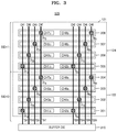
FIG. 3 is a diagram for describing a portion of a structure of the memory device of FIG. 2.
Referring to FIGS. 2 and 3, the memory device 120 includes a plurality of stacked memory layers 301 to 308. For example, the memory device 120 may be an HBM. The memory layers 301 to 308 may be referred to as core dies. The memory layers 301 to 308 may constitute a plurality of independent interfaces called channels. The memory layers 301 to 308 may each include two channels. For conceptual description of the inventive concept and simplification of the drawings, FIG. 3 shows an example configuration in which odd-numbered channels (e.g., CH1 a, CH3 a, CH5 a, CH7 a, CH1 b, CH3 b, CH5 b, and CH7 b) are arranged on the left side of the memory layers 301 to 308 and even-numbered channels (e.g., CH2 a, CH4 a, CH6 a, CH8 a, CH2 b, CH4 b, CH6 b, and CH8 b) are arranged on the right side of the memory layers 301 to 308, but the arrangement of the memory layers 301 to 308 according to the inventive concept is not limited thereto.
For example, a first memory layer 301 may include a channel CH1 a and a channel CH2 a, a second memory layer 302 may include a channel CH3 a and a channel CH4 a, a third memory layer 303 may include a channel CH5 a and a channel CH6 a, and a fourth memory layer 304 may include a channel CH7 a and a channel CH8 a. A fifth memory layer 305 may include a channel CH1 b and a channel CH2 b, a sixth memory layer 306 may include a channel CH3 b and a channel CH4 b, a seventh memory layer 307 may include a channel CH5 b and a channel CH6 b, and an eighth memory layer 308 may include a channel CH7 b and a channel CH8 b. In the present embodiment of FIG. 3, an example of the memory device 120 is illustrated as in which eight memory layers 301 to 308 are stacked. However, the inventive concept is not limited thereto. According to embodiments, various numbers of memory layers (e.g., 2, 4, etc.) may be stacked in the memory device 120.
The memory device 120 may further include a buffer die 310 below the stacked memory layers 301 to 308. The buffer die 310 may be referred to as a memory buffer. The buffer die 310 may include an input buffer (or a receiver) that receives the clock signal CK, the command CMD, the address ADDR, and the data DQ from the memory controller 112 (FIG. 1). The buffer die 310 may provide a signal distribution function and a data input/output function with respect to channels CH1 a, CH2 a, CH3 a, CH4 a, CH5 a, CH6 a, CH7 a, CH8 a, CH1 b, CH2 b, CH3 b, CH4 b, CH5 b, CH6 b, CH7 b, and CH8 b through silicon vias TSV1 to TSV8. The buffer die 310 may communicate with the memory controller 112 through conductive units like bumps or solder balls formed on an outer surface of the memory device 120.
The buffer die 310 may include the PIM command converter 126, the PIM mode selector 210, the first switch 231, the second switch 232, the PIM engine 250 and the data input/output circuit 260 described above with reference to FIG. 2.
The stacked memory layers 301 to 308 may correspond to the memory cell array 121 including the PIM region 122 and the normal memory region 124 described above with reference to FIG. 2. Lower four memory layers 301 to 304 from among the stacked memory layers 301 to 308 may be allocated to the PIM region 122, whereas upper four memory layers 305 to 308 may be allocated to the normal memory region 124. According to exemplary embodiment of the inventive concept, the lower four memory layers 301 to 304 from among the stacked memory layers 301 to 308 are allocated to the normal memory region 124, and the upper four memory layers 305 to 308 are allocated to the PIM region 122.
The memory layers 301 to 304 of the PIM region 122 and the memory layers 305 to 308 of the normal memory region 124 may form common channels CH1 to CH8 through the through silicon vias TSV1 to TSV8 and electrode pads P1 a, P2 a, P3 a, P4 a, P5 a, P6 a, P7 a, P8 a, P1 b, P2 b, P3 b, P4 b, P5 b, P6 b, P7 b, and P8 b that are electrically connected to the through silicon vias TSV1 to TSV8. For simplicity of the drawings, the electrode pads P1 a, P2 a, P3 a, P4 a, P5 a, P6 a, P7 a, P8 a, P1 b, P2 b, P3 b, P4 b, P5 b, P6 b, P7 b, and P8 b are shown as circles. It may be understood that the electrode pads P1 a, P2 a, P3 a, P4 a, P5 a, P6 a, P7 a, P8 a, P1 b, P2 b, P3 b, P4 b, P5 b, P6 b, P7 b, and P8 b are electrically connected to the through silicon vias TSV1 to TSV8, respectively.
For example, the channel CH1 a of the first memory layer 301 may be connected to through silicon vias TSV1 through an electrode pad P1 a, and a channel CH1 b of the fifth memory layer 305 may be connected to the through silicon vias TSV1 through an electrode pad P1 b. The channel CH1 a and the channel CH1 b electrically connected to the through silicon vias TSV1 may form a first common channel CH1. Also, a channel CH2 a of the first memory layer 301 may be connected to through silicon vias TSV2 through an electrode pad P2 a, and a channel CH2 b of the fifth memory layer 305 may be connected to the through silicon vias TSV2 through an electrode pad P2 b. The channel CH2 a and the channel CH2 b electrically connected to the through silicon vias TSV2 may form a second common channel CH2.
A channel CH3 a of the second memory layer 302 may be connected to through silicon vias TSV3 through an electrode pad P3 a, and a channel CH3 b of the sixth memory layer 306 may be connected to the through silicon vias TSV3 through an electrode pad P3 b. The channel CH3 a and the channel CH3 b electrically connected to the through silicon vias TSV3 may form a third common channel CH3. Also, a channel CH4 a of the second memory layer 302 may be connected to through silicon vias TSV4 through an electrode pad P4 a, and a channel CH4 b of the sixth memory layer 306 may be connected to the through silicon vias TSV4 through an electrode pad P4 b. The channel CH4 a and the channel CH4 b electrically connected to the through silicon vias TSV4 may form a fourth common channel CH4.
A channel CH5 a of the third memory layer 303 may be connected to through silicon vias TSV5 through an electrode pad P5 a, and a channel CH5 b of the seventh memory layer 307 may be connected to the through silicon vias TSV5 through an electrode pad P5 b. The channel CH5 a and the channel CH5 b electrically connected to the through silicon vias TSV5 may form a fifth common channel CH5. Also, a channel CH6 a of the third memory layer 303 may be connected to through silicon vias TSV6 through an electrode pad P6 a, and a channel CH6 b of the seventh memory layer 307 may be connected to the through silicon vias TSV6 through an electrode pad P6 b. The channel CH6 a and the channel CH6 b electrically connected to the through silicon vias TSV6 may form a sixth common channel CH6.
A channel CH7 a of the fourth memory layer 304 may be connected to through silicon vias TSV7 through an electrode pad P7 a, and a channel CH7 b of the eighth memory layer 308 may be connected to the through silicon vias TSV7 through an electrode pad P7 b. The channel CH7 a and the channel CH7 b electrically connected to the through silicon vias TSV7 may form a seventh common channel CH7. Also, a channel CH8 a of the fourth memory layer 304 may be connected to through silicon vias TSV8 through an electrode pad P8 a, and a channel CH8 b of the eighth memory layer 308 may be connected to the through silicon vias TSV8 through an electrode pad P8 b. The channel CH8 a and the channel CH8 b electrically connected to the through silicon vias TSV8 may form an eighth common channel CH8.
First to eighth common channels CH1 to CH8 of the memory cell array 121 may be connected to the buffer die 310. In the first to eighth common channels CH1 to CH8, the PIM region 122 and the normal memory region 124 may be selectively accessed according to a stack identification signal SID that distinguishes the lower memory layers 301 to 304 and the upper memory layers 305 to 308. For example, when the stack identification signal SID is logic “0”, the lower memory layers 301 to 304 (i.e., the PIM region 122) from among the first through eighth common channels CH1 to CH8 may be accessed. When the stack identification signal SID is logic “1”, the upper memory layers 305 to 308 (i.e., the normal memory region 124) from among the first through eighth common channels CH1 to CH8 may be accessed.
As described above with reference to FIG. 2, when the memory device 120 operates in the internal processing mode, the PIM region 122 may be accessed. In an exemplary embodiment, when the stack identification signal SID set to a logic “0” is included in the address ADDR received through the command/address signal lines 132 of the memory bus 130 and the PIM mode selection signal PIM_SEL is activated by the PIM mode selector 210, the memory device 120 operates in the internal processing mode. Since the PIM mode selection signal PIM_SEL is activated, the memory device 120 may access the PIM region 122 and operate in the internal processing mode.
When the memory device 120 operates in the normal mode, the normal memory region 124 may be accessed. In an exemplary embodiment, when the stack identification signal SID offset to a logic “1” is included in the address ADDR received through the command/address signal lines 132 of the memory bus 130, and the PIM mode selection signal PIM_SEL is deactivated by the PIM mode selector 210, the memory device 120 operates in the normal mode. Since the PIM mode selection signal PIM_SEL is deactivated, the memory device 120 may access the normal memory region 124 and operate in the normal mode.
In the present embodiment, the stack identification signal SID may be a specific address, which is stored in the control register 116 and divides the memory cell array 121 of the memory controller 112 into the PIM region 122 and the normal memory region 124. Also, the stack identification signal SID may be a specific address used to address the PIM region 122 recognized by the PIM mode selector 210.
FIG. 4 is a diagram for describing a portion of a structure of the memory device of FIG. 2.
Referring to FIG. 4, a memory device 120 a is different from the memory device 120 of FIG. 3 in that the memory cell array 121 includes first to fourth memory layers 301 to 304. Hereinafter, descriptions regarding the memory device 120 a identical to those given above with reference to FIG. 3 will be omitted.
In the memory cell array 121 of the memory device 120 a, first and second memory layers 301 and 302 may be allocated to PIM region 122, whereas third and fourth memory layers 303 and 304 may be allocated to the normal memory region 124. According to an exemplary embodiment of the inventive concept, the first and second memory layers 301 and 302 are allocated to the normal memory region 124, and the third and fourth memory layers 303 and 304 are allocated to the PIM region 122.
Eight channels CH1 a to CH8 a of the first through fourth memory layers 301 to 304 may be connected to the buffer die 310 through the through silicon vias TSV1 TSV8, respectively. The eight channels CH1 a to CH8 a may be addressed by a 3-bit channel address. When the most significant bit of a channel address is “0”, channels CH1 a, CH2 a, CH3 a, and CH4 a of the first and second memory layers 301 and 302 may be selected. On the contrary, when the most significant bit of the channel address is “1”, channels CH5 a, CH6 a, CH7 a, and CH8 a of the third and fourth memory layers 303 and 304 may be selected. As a result, the PIM region 122 and the normal memory region 124 may be selectively accessed according to the most significant bit of the channel address.
The most significant bit of the channel address is a specific address that divides the memory cell array 121 of the memory device 120 a into the PIM region 122 and the normal memory region 124 and may be stored in the control register 116 of the memory controller 112. Also, the most significant bit of the channel address may be a specific address used to address the PIM region 122 recognized by the PIM mode selector 210.
FIG. 5 is a diagram for describing a portion of a structure of a memory cell array of FIG. 2.
Referring to FIG. 5, the memory cell array 121 may include, for example, eight banks BANK1 to BANK8. First to fourth banks BANK to BANK4 may be allocated to the PIM region 122, and fifth to eighth banks BANK5 to BANK8 may be allocated to the normal memory region 124. The eight banks BANK1 to BANK8 may be addressed by a 3-bit bank address. When the most significant bit of a bank address is “0”, the first to fourth banks BANK1 to BANK4 may be selected. On the contrary, when the most significant bit of the bank address is “1”, the fifth to eighth banks BANK5 to BANK8 may be selected. As a result, the PIM region 122 and the normal memory region 124 may be selectively accessed according to the most significant bit of the bank address.
The most significant bit of the bank address is a specific address that divides the memory cell array 121 into the PIM region 122 and the normal memory region 124 and may be stored in the control register 116 of the memory controller 112. Also, the most significant bit of the bank address may be a specific address used to address the PIM region 122 recognized by the PIM mode selector 210.
The PIM region 122 and the normal memory region 124 described above with reference to FIGS. 3 to 5 are examples that are set as fixed regions in the memory cell array 121 by the stack identification signal SIDs, a channel address, or a bank address. Specific address information for setting the PIM region 122 and the normal memory region 124 as fixed regions may be statically set in the control register 116 of the memory controller 112.
According to embodiments of the inventive concept, the PIM region 122 and the normal memory region 124 are set as variable regions in the memory cell array 121 according to combinations of the stack identification signal SID, a channel address, and/or a bank address. Specific address information for setting the PIM region 122 and the normal memory region 124 as variable regions may be dynamically set in the control register 116 of the memory controller 112.
FIG. 6 is a flowchart for describing an operation of the memory device of FIG. 2 according to an exemplary embodiment of the inventive concept.
Referring to FIGS. 1, 2, and 6, in operation S610, the memory device 120 provides specific address information regarding the PIM region 122 and the normal memory region 124 of the memory cell array 121 to the memory controller 112. The specific address information may include specific addresses that divide the memory cell array 121 into a PIM region 122 and a normal memory region 124. The specific address is an address used to address the PIM region 122 and may include, for example, the stack identification signal SID, a channel address, and/or a bank address. The specific address information may be stored in the control register 116 of the memory controller 112.
In operation S620, the memory device 120 receives a specific address together with the command CMD from the memory controller 112 through the command/address signal lines 132. The memory controller 112 may issue the command CMD for accessing the memory device 120 based on a memory request of the host device 110. In this case, the command CMD and the specific address may be provided through the memory PHY 114, which supports the DDR protocol and/or the LPDDR protocol of the JEDEC standard, between the memory controller 112 and the memory device 120. For example, it is assumed that a specific address is the stack identification signal SID, as described above with reference to FIG. 3.
In operation S630, the memory device 120 determines whether the stack identification signal SID received as the specific address together with the command CMD in operation S620 addresses the PIM region 122 of the memory cell array 121. As described above with reference to FIG. 3, when the stack identification signal SID is provided as logic “0”, the lower memory layers 301 to 304, that is, the PIM region 122, from among the first through eighth common channels CH1 to CH8 may be accessed. On the contrary, when the stack identification signal SID is provided as logic “1”, the upper memory layers 305 to 308, that is, the normal memory region 124, from among the first through eighth common channels CH1 to CH8 may be accessed.
When the stack identification signal SID is logic “0”, in operation S640, the memory device 120 enters the internal processing mode. The PIM mode selector 210 of the memory device 120 may activate the PIM mode selection signal PIM_SEL in response to the stack identification signal SID of logic “0”. By activating the PIM mode selection signal PIM_SEL, the memory device 120 may operate in the internal processing mode.
In operation S641, the memory device 120 converts the command CMD received in operation S620 into the internal processing operation command PIM_CMD. The PIM command converter 126 of the memory device 120 may convert the received command CMD into the internal processing operation command PIM_CMD that instructs a type of an internal processing operation, e.g., data search, data arithmetic operation (e.g., add, subtract, multiple, divide, etc.), data move, data inversion, data shift, data swap, data comparison, logic operations, and/or data processing/operations.
In operation S642, the memory device 120 performs an internal processing operation according to the internal processing operation command PIM_CMD. The PIM engine 250 of the memory device 120 may perform an internal processing operation by using the PIM region 122 of the memory cell array 121 according to the internal processing operation command PIM_CMD. The PIM engine 250 may store internal processing data, which is a result of the internal processing operation performed in response to the internal processing operation command PIM_CMD, in the PIM region 122. Alternatively, the PIM engine 250 may read internal processing data from the PIM region 122 in response to the internal processing operation command PIM_CMD and perform an internal processing operation based on the read internal processing data. When the internal processing operation of operation S642 has completed, the memory device 120 may proceed to operation S620 and receive a next command CMD with a specific address.
In operation S640, when the stack identification signal SID is not logic “0”, the memory device 120 enters the normal mode in operation S650. The PIM mode selector 210 of the memory device 120 may deactivate the PIM mode selection signal PIM_SEL in response to the stack identification signal SID of logic “1”. By deactivating the PIM mode selection signal PIM_SEL, the memory device 120 may operate in the normal mode.
In operation S651, the memory device 120 performs a data transaction operation according to the command CMD received in operation S620. The command CMD may be associated with a data transaction operation performed in the normal mode. The memory device 120 may store (write) the data DQ received from the memory controller 112 through the data lines 134 in the normal memory region 124 of the memory cell array 121 according to the command CMD, read data from the normal memory region 124, and transmit the read data to the memory controller 112 through the data lines 134 as the data DQ. When the data transaction operation of operation S651 has completed, the memory device 120 may proceed to operation S620 and receive a next command CMD with a specific address.
FIG. 7 is a timing diagram for describing an operation of a memory device of FIG. 2. FIG. 7 shows a timing diagram of an operation based on the clock signal CK according to the DDR protocol and/or the LPDDR protocol. For simplicity of the drawing and convenience of explanation, FIG. 7 conceptually shows a write operation and a read operation in which the data DQ is input/output to/from the memory device 120 through the data lines 134.
Referring to FIGS. 1, 2, and 7, at a time point Ta, the memory device 120 receives the address ADDR including the stack identification signal SID from the memory controller 112 together with a read command RD. At this time, the stack identification signal SID is set to logic “0”. Although not shown, an active command associated with the read command RD may be received from the memory controller 112 before the time point Ta.
In response to logic “0” of the stack identification signal SID at the time point Ta, the memory device 120 enters the internal processing mode. In the internal processing mode, the read command RD is converted into an internal processing read command by the PIM command converter 126, and the PIM engine 250 reads internal processing data written to memory cells corresponding to the address ADDR in the PIM region 122 of the memory cell array 121 according to the internal processing read command and performs an internal processing operation by using the read internal processing data. The present embodiment shows a case in which the internal processing data read from the PIM region 122 is not transmitted to the memory controller 112 outside the memory device 120. According to another embodiment, internal processing data processed by the PIM engine 250 is transmitted to the memory controller 112 as the data DQ through the data lines 134 of the memory bus 130.
At a time point Tb, the memory device 120 receives the address ADDR including the stack identification signal SID from the memory controller 112 together with the read command RD. At this time, the stack identification signal SID is set to logic “1”.
In response to logic “1” of the stack identification signal SID at the time point Tb, the memory device 120 enters the normal mode. In the normal mode, the memory device 120 reads data D written to memory cells corresponding to the address signal ADDR in the normal memory region 124 of the memory cell array 121 according to the read command RD. The read data D may be transmitted to the memory controller 112 as the data DQ through the data lines 134 of the memory bus 130.
At a time point Tc, the memory device 120 receives the address ADDR including the stack identification signal SID from the memory controller 112 together with a write command WR. At this time, the stack identification signal SID is set to a logic “0”.
In response to logic “0” of the stack identification signal SID at the time point Tc, the memory device 120 enters the internal processing mode. In the internal processing mode, the write command WR is converted into an internal processing write command by the PIM command converter 126, and the PIM engine 250 writes internal processing data obtained as a processing result of performing an internal processing operation to memory cells corresponding to the address ADDR in the PIM region 122 of the memory cell array 121 according to the internal processing write command.
At a time point Td, the memory device 120 receives the address ADDR including the stack identification signal SID from the memory controller 112 together with the write command WR. At this time, the stack identification signal SID is set to a logic “1”.
In response to logic “1” of the stack identification signal SID at the time point Td, the memory device 120 enters the normal mode. In the normal mode, the memory device 120 writes data D to memory cells corresponding to the address signal ADDR in the normal memory region 124 of the memory cell array 121 according to the write command WR. Here, the data D to be written may be received from the memory controller 112 as the data DQ through the data lines 134 of the memory bus 130.
A timing parameter called CAS-to-CAS delay tCCD, which is the minimum time interval needed between successive read commands, exists between the read command RD at the time point Ta and the read command RD at the time point Tb. Also, a timing parameter tCCD, which is the minimum time interval needed between successive write commands, exists between the write command WR at the time point Tc and the write command WR at the time point Td. The timing parameter tCCD between the time point Ta and the time point Tb may satisfy the tCCD timing parameter requirements defined in the DDR specification and/or the LPDDR specifications of the JEDEC standard. Also, the timing parameter tCCD between the time point Tc and the time point Td may satisfy the tCCD timing parameter requirements defined in the DDR specification and/or the LPDDR specifications of the JEDEC standard.
A timing parameter called Read-to-Write delay tRTW exists between the read command RD at the time point Tb and the write command WR at the time point Tc. The timing parameter tRTW between the time point Tb and the time point Tc may satisfy the tRTW timing parameter requirements defined in the DDR specification and/or the LPDDR specifications of the JEDEC standard.
FIG. 8 is a diagram for describing a PIM mode selector of FIG. 2.
Referring to FIG. 8, compared with the PIM mode selector 210 of FIG. 2, a PIM mode selector 210 a determines whether addresses ADDRs received together with the command CMD coincide with a PIM mode entering code and whether the addresses ADDRs coincide with a PIM mode exiting code, instead of determining whether the addresses ADDRs received through the command/address signal lines 132 of the memory bus 130 together with the command CMD include a specific address used to address the PIM region 122.
The PIM mode selector 210 a includes a PIM mode entering check circuit 810, a PIM mode exit check circuit 820, and a PIM mode selection signal generation circuit 830.
The PIM mode entering check circuit 810 may store a PIM mode entering code, compare bit values of the addresses ADDRs sequentially received by the PIM mode selector 210 a with bit values of the PIM mode entering code, and, as a result of the comparison, output a PIM mode entering signal PIM_ENTER. When the bit values of the sequential addresses ADDRs coincide with the bit values of the PIM mode entering code, the PIM mode entering check circuit 810 may output the PIM mode entering signal PIM_ENTER of logic “1”. Otherwise, the PIM mode entering check circuit 810 may output the PIM mode entering signal of logic “0”. The PIM mode entering signal PIM_ENTER may be provided to the PIM mode selection signal generation circuit 830.
In the PIM mode entering code, for example, bit values of addresses respectively corresponding to sequential write commands WR may be set as a back-to-back address sequence, e.g., 0xFFFF, 0x1F1F, 0xAAFF, 0x0000, 0x1111, 0x4444, 0x3333, and 0x0000. For example, if the memory controller 112 transmits a first write command along with a first address of 0xFFFF at time 1, a second write command along with a second address of 0x1F1F at time 2, transmits a third write command along with a third address of 0xAAFF at time 3, transmits a fourth write command along with a fourth address of 0x0000 at time 4, a fifth write command along with a fifth address of 0x1111 at time 5, transmits a sixth write command along with a sixth address of 0x4444 at time 6, transmits a seventh write command along with a seventh address of 0x3333 at time 7, and transmits an eight write command along with an eighth address of 0x0000 at time 8, the PIM mode selector 210 a may interpret receipt of such a sequence (i.e., the back-to-back-address) as instructing it to output the PIM mode entering signal PIM_ENTER of logic “1”. While the above describes a sequence of 8 pairs of commands and addresses to send the back-to-back address representing the PIM Mode Enter Code, embodiments of the inventive concept are not limited thereto. For example, there may be less than 8 pairs or more than 8 pairs in alternate embodiments. Further, while the above describes use of bit values 0xFFFF, 0x1F1F, 0xAAFF, 0x0000, 0x1111, 0x4444, 0x3333, and 0x0000, embodiments of the inventive concept are not limited thereto. For example, the bit values may have different values in alternate embodiments.
The PIM mode exit check circuit 20 may store a PIM mode exiting code, compare bit values of the addresses ADDRs sequentially received by the PIM mode selector 210 a with bit values of the PIM mode exiting code, and, as a result of the comparison, output a PIM mode exiting signal PIM_EXIT. When the bit values of sequential addresses ADDRs coincide with the bit values of the PIM mode exiting code, the PIM mode exit check circuit 20 may output the PIM mode exiting signal PIM_EXIT of logic “1”. Otherwise, the PIM mode exit check circuit 20 may output the PIM mode exiting signal PIM_EXIT of logic “0”. The PIM mode exiting signal PIM_EXIT may be provided to the PIM mode selection signal generation circuit 830.
In the PIM mode exiting code, for example, bit values of addresses respectively corresponding to the sequential write commands WR may be set as a back-to-back address sequence, e.g., 0x0000, 0x2F2F, 0xFFAA, 0x0000, 0x6666, 0xF2F3, 0x2333, and 0xFFFF. For example, if the memory controller 112 transmits a ninth write command along with a ninth address of 0x0000 at time 9, a tenth write command along with a tenth address of 0x2F2F at time 10, transmits an eleventh write command along with an eleventh address of 0xFFAA at time 11, transmits a twelfth write command along with a twelfth address of 0x0000 at time 12, a thirteenth write command along with a thirteenth address of 0x6666 at time 13, transmits a fourteenth write command along with a fourteenth address of 0xF2F3 at time 14, transmits a fifteenth write command along with a fifteenth address of 0x2333 at time 15, and transmits a sixteenth write command along with a sixteenth address of 0xFFFF at time 16, the PIM mode selector 210 a may interpret receipt of such a sequence (i.e., the back-to-back-address) as instructing it to output the PIM mode exiting signal PIM_EXIT of logic “0”. While the above describes a sequence of 8 pairs of commands and addresses to send the back-to-back address representing the PIM Mode Exit Code, embodiments of the inventive concept are not limited thereto. For example, there may be less than 8 pairs or more than 8 pairs in alternate embodiments. Further, while the above describes use of bit values 0x0000, 0x2F2F, 0xFFAA, 0x0000, 0x6666, 0xF2F3, 0x2333, and 0xFFFF, embodiments of the inventive concept are not limited thereto. For example, the bit values may have different values in alternate embodiments
The PIM mode selection signal generation circuit 830 may generate a PIM mode selection signal PIM_SEL based on the PIM mode entering signal PIM_ENTER and the PIM mode exiting signal PIM_EXIT. The PIM mode selection signal generation circuit 830 may activate the PIM mode selection signal PIM_SEL in response to the PIM mode entering signal PIM_ENTER of logic “1” and the PIM mode exiting signal PIM_EXIT of logic “0”. By activating the PIM mode selection signal PIM_SEL, the memory device 120 may operate in the internal processing mode.
The PIM mode selection signal generation circuit 830 may deactivate the PIM mode selection signal PIM_SEL in response to the PIM mode entering signal PIM_ENTER of logic “0” or the PIM mode exiting signal PIM_EXIT of logic “1”. By deactivating the PIM mode selection signal PIM_SEL, the memory device 120 may operate in the normal mode.
The PIM mode entering code and the PIM mode exiting code described above with reference to FIG. 8 are merely an example, and the inventive concept is not limited thereto. According to embodiments of the inventive concept, the PIM mode entering code and the PIM mode exiting code may be configured in various ways. The PIM mode entering code and the PIM mode exiting code may be stored in the control register 116 of the memory controller 112 and the PIM mode selector 210 a as same code values.
FIG. 9 is a flowchart for describing an operation of the memory device of FIG. 2 according to an exemplary embodiment of the inventive concept.
Referring to FIGS. 1, 2, 8, and 9, in operation S905, the memory device 120 sequentially receives the command CMD and the addresses ADDRs from the memory controller 112 through the command/address signal lines 132.
In operation S911, through the PIM mode entering check circuit 810 of the PIM mode selector 210 a, the memory device 120 compares bit values of sequentially received addresses ADDRs with bit values of the PIM mode entering code, and, as a result of the comparison, outputs the PIM mode entering signal PIM_ENTER.
In operation S912, through the PIM mode exit check circuit 820 of the PIM mode selector 210 a, the memory device 120 compares the bit values of the sequentially received addresses ADDRs with bit values of the PIM mode exiting code, and, as a result of the comparison, outputs the PIM mode exiting signal PIM_EXIT.
In operation S920, through the PIM mode selection signal generation circuit 830 of the PIM mode selector 210 a, the memory device 120 generates the PIM mode selection signal PIM_SEL based on the PIM mode entering signal PIM_ENTER and the PIM mode exiting signal PIM_EXIT. For example, the PIM mode selection signal generation circuit 830 may activate the PIM mode selection signal PIM_SEL in response to the PIM mode entering signal PIM_ENTER of logic “1” and the PIM mode exiting signal PIM_EXIT of logic “0”. The PIM mode selection signal generation circuit 830 may deactivate the PIM mode selection signal PIM_SEL in response to the PIM mode entering signal PIM_ENTER of logic “0” or the PIM mode exiting signal PIM_EXIT of logic “1”.
In operation S930, the memory device 120 determines whether the PIM mode selection signal PIM_SEL generated in operation S920 is activated.
When the PIM mode selection signal PIM_SEL is activated, in operation S940, the memory device 120 enters the internal processing mode.
In operation S941, the memory device 120 converts the command CMD received in operation S920 into the internal processing operation command PIM_CMD. The PIM command converter 126 of the memory device 120 may convert the received command CMD into the internal processing operation command PIM_CMD that instructs a type of an internal processing operation, e.g., data search, data arithmetic operation (e.g., add, subtract, multiple, divide, etc.), data move, data inversion, data shift, data swap, data comparison, logic operations, and/or data processing/operations.
In operation S942, the memory device 120 performs an internal processing operation according to the internal processing operation command PIM_CMD. The PIM engine 250 of the memory device 120 may perform an internal processing operation by using the PIM region 122 of the memory cell array 121 according to the internal processing operation command PIM_CMD. The PIM engine 250 may store internal processing data, which is a result of an internal processing operation performed in response to the internal processing operation command PIM_CMD, in the PIM region 122. Alternatively, the PIM engine 250 may read internal processing data from the PIM region 122 in response to the internal processing operation command PIM_CMD and perform an internal processing operation based on the read internal processing data.
Meanwhile, when it is determined in operation S930 that the PIM mode selection signal PIM_SEL is deactivated, in operation S950, the memory device 120 enters the normal mode.
In operation S951, the memory device 120 performs a data transaction operation according to the command CMD received in operation S905. The command CMD may be associated with a data transaction operation performed in the normal mode. The memory device 120 may store the data DQ received from the memory controller 112 through the data lines 134 in the normal memory region 124 of the memory cell array 121 according to the command CMD, read the data DQ from the normal memory region 124, and transmit the read data to the memory controller 112 through the data lines 134 as the data DQ.
While the inventive concept has been particularly shown and described with reference to embodiments thereof, it will be understood that various changes in form and details may be made therein without departing from the spirit and scope of the inventive concept.

Claims (19)

What is claimed is:
1. A memory device comprising:
a memory cell array comprising a first memory region and a second memory region;
signal lines configured to receive a command and an address from a source located outside the memory device;
a mode selector circuit configured to activate a processing mode selection signal for controlling the memory device to enter an internal processing mode when the address received together with the command includes a specific address used to distinguish the first memory region from the second memory region;
a command converter circuit configured to convert the received command into an internal processing operation command in response to the activate of the processing mode selection signal; and
an internal processor configured to perform an internal processing operation on the first memory region in response to the internal processing operation command, in the internal processing mode.
2. The memory device of claim 1, wherein the signal lines are connected to a memory physical layer interface, which supports a double data rate (DDR) protocol or a low power double data rate (LPDDR) protocol and the memory physical layer interface is located outside the memory device.
3. The memory device of claim 1, wherein the memory cell array comprises stacked memory layers, the stacked memory layers include common channels, through silicon vias and electrode pads electrically connected to the through silicon vias, and, in the common channels, the stacked memory layers belonging to the first memory region and the stacked memory layers belonging to the second memory region are selectively accessed according to a stack identification signal, and the specific address comprises the stack identification signal for accessing the stacked memory layers belonging to the first memory region.
4. The memory device of claim 1, wherein the memory cell array comprises stacked memory layers, the stacked memory layers include common channels, through silicon vias and electrode pads electrically connected to the through silicon vias, and, in the common channels, the stacked memory layers belonging to the first memory region and the stacked memory layers belonging to the second memory region are selectively accessed according to a channel address, and the specific address comprises the channel address for accessing the stacked memory layers belonging to the first memory region.
5. The memory device of claim 1, wherein the memory cell array comprises a plurality of banks, from among the banks, banks belonging to the first memory region and banks belonging to the second memory region are selectively accessed according to a bank address, and the specific address comprises the bank address for accessing the banks belonging to the first memory region.
6. The memory device of claim 1, wherein the first memory region and the second memory region are set to fixed regions by the specific address.
7. The memory device of claim 1, wherein the first memory region and the second memory region are set to variable regions by the specific address.
8. The memory device of claim 1, wherein, when the specific address is not included in the address received with the command, the mode selector circuits deactivates the processing mode selection signal, such that the memory device enters a normal mode.
9. The memory device of claim 1, wherein the memory device sequentially receives first commands through the signal lines and sequentially receives addresses respectively corresponding to the sequentially received first commands, and the mode selector circuit determines whether the sequentially received addresses coincide with an internal processing mode entering code and an internal processing mode exiting code and generates the processing mode selection signal based on a result of the determination.
10. The memory device of claim 9, wherein the mode selector circuit activates the processing mode selection signal when the sequentially received addresses coincide with the internal processing mode entering code and the sequentially received addresses do not coincide with the internal processing mode exiting code.
11. The memory device of claim 9, wherein the mode selector circuit deactivates the processing mode selection signal, such that the memory device enters a normal mode, when the sequentially received addresses do not coincide with the internal processing mode entering code and the sequentially received addresses coincide with the internal processing mode exiting code.
12. A method of operating a memory device comprising a memory cell array comprising a first memory region and a second memory region, and internal processor configured to perform an internal processing operation, the method comprising:
receiving a command and an address from a source located outside the memory device through a pre-defined protocol interface;
activating a processing mode selection signal for controlling the memory device to enter an internal processing mode when the address received together with the command includes a specific address used to distinguish the memory region from the second memory region;
converting the received command into an internal processing operation command in response to the activation of the processing mode selection signal; and
performing, by the internal processor, an internal processing operation on the first memory region in response to the internal processing operation command, in the internal processing mode.
13. The method of claim 12, wherein the pre-defined protocol interface is a memory physical layer interface, which supports a double data rate (DDR) protocol or a low power double data rate (LPDDR) protocol.
14. The method of claim 12, wherein the generating of the processing mode selection signal comprises:
deactivating the internal processing mode selection signal when the specific address is not included in the address received with the command.
15. The method of claim 14, further comprising entering a normal mode in response to deactivation of the processing mode selection signal.
16. The method of claim 14, wherein the specific address comprises a stack identification signal for addressing the first memory region, a channel address, or a bank address.
17. The method of claim 14, wherein the first memory region and the second memory region are set to fixed regions by the specific address.
18. A memory system comprising:
a memory device,
wherein the memory device comprises:
a memory cell array comprising a first memory region and a second memory region;
a mode selector circuit configured to receive an address from a memory controller, generate a processing mode selection signal indicating an internal processing mode when the address is located within a predefined range, and generate the processing mode selection signal indicating a normal mode when the address is outside the range;
a command converter circuit;
a switching circuit configured to provide a command received from the memory controller together with the address to the command converter circuit during the internal processing mode to convert the command into an internal processing operation command and provide the command to the memory cell array during the normal mode;
an internal processor configured to perform an internal processing operation on the first memory region in response to the internal processing operation command, in the internal processing mode.
19. The memory system of claim 18, wherein the memory device supports a double data rate (DDR) protocol or a low power double data rate (LPDDR) protocol.
US16/813,851 2019-03-11 2020-03-10 Method of performing internal processing operations with pre-defined protocol interface of memory device Active US11158357B2 (en)

Priority Applications (2)

Application Number Priority Date Filing Date Title
US16/813,851 US11158357B2 (en) 2019-03-11 2020-03-10 Method of performing internal processing operations with pre-defined protocol interface of memory device
US17/504,918 US20220036929A1 (en) 2019-03-11 2021-10-19 Method of performing internal processing operations with pre-defined protocol interface of memory device

Applications Claiming Priority (4)

Application Number Priority Date Filing Date Title
US201962816509P 2019-03-11 2019-03-11
KR10-2019-0161673 2019-12-06
KR1020190161673A KR20200108772A (en) 2019-03-11 2019-12-06 Method of performing internal processing operations with pre-defined protocol interface of memory device
US16/813,851 US11158357B2 (en) 2019-03-11 2020-03-10 Method of performing internal processing operations with pre-defined protocol interface of memory device

Related Child Applications (1)

Application Number Title Priority Date Filing Date
US17/504,918 Continuation US20220036929A1 (en) 2019-03-11 2021-10-19 Method of performing internal processing operations with pre-defined protocol interface of memory device

Publications (2)

Publication Number Publication Date
US20200294558A1 US20200294558A1 (en) 2020-09-17
US11158357B2 true US11158357B2 (en) 2021-10-26

Family

ID=72289581

Family Applications (2)

Application Number Title Priority Date Filing Date
US16/813,851 Active US11158357B2 (en) 2019-03-11 2020-03-10 Method of performing internal processing operations with pre-defined protocol interface of memory device
US17/504,918 Pending US20220036929A1 (en) 2019-03-11 2021-10-19 Method of performing internal processing operations with pre-defined protocol interface of memory device

Family Applications After (1)

Application Number Title Priority Date Filing Date
US17/504,918 Pending US20220036929A1 (en) 2019-03-11 2021-10-19 Method of performing internal processing operations with pre-defined protocol interface of memory device

Country Status (3)

Country Link
US (2) US11158357B2 (en)
CN (1) CN111679786A (en)
DE (1) DE102020105628A1 (en)

Families Citing this family (6)

* Cited by examiner, † Cited by third party
Publication number Priority date Publication date Assignee Title
US11908541B2 (en) * 2020-01-07 2024-02-20 SK Hynix Inc. Processing-in-memory (PIM) systems
US11467834B2 (en) * 2020-04-01 2022-10-11 Samsung Electronics Co., Ltd. In-memory computing with cache coherent protocol
CN115469800A (en) 2021-06-10 2022-12-13 三星电子株式会社 Data processing system and method for accessing heterogeneous memory system
KR20230043619A (en) * 2021-09-24 2023-03-31 삼성전자주식회사 Memory device and method of implementing reducing timimg parameters and power comsumption of internal processing operations
US20230205706A1 (en) * 2021-12-23 2023-06-29 Advanced Micro Devices, Inc. Approach for managing near-memory processing commands and non-near-memory processing commands in a memory controller
US20240070068A1 (en) * 2022-08-26 2024-02-29 Samsung Electronics Co., Ltd. Device and method with memory request processing using memory address space extension

Citations (23)

* Cited by examiner, † Cited by third party
Publication number Priority date Publication date Assignee Title
US5678021A (en) 1992-08-25 1997-10-14 Texas Instruments Incorporated Apparatus and method for a memory unit with a processor integrated therein
US20100312998A1 (en) 2009-06-04 2010-12-09 Micron Technology, Inc. Direct communication with a processor internal to a memory device
US20110231827A1 (en) 2010-03-22 2011-09-22 Kilbane Stephen M Methods and apparatus for debugging programs in shared memory
US20120215991A1 (en) 2011-02-23 2012-08-23 Freescale Semiconductor, Inc. Memory protection unit (mpu) having a shared portion and method of operation
US20130036314A1 (en) 2011-08-04 2013-02-07 Glew Andrew F Security perimeter
US20130169642A1 (en) 2011-12-29 2013-07-04 Qualcomm Incorporated Packing multiple shader programs onto a graphics processor
US20140281149A1 (en) 2013-03-15 2014-09-18 Micron Technology, Inc. Apparatuses and methods for adaptive control of memory
US20150046660A1 (en) 2010-11-23 2015-02-12 IP Cube Partners (ICP) Co., Ltd. Active memory processor system
US9268704B2 (en) 2012-11-27 2016-02-23 International Business Machines Corporation Low latency data exchange
US9329804B2 (en) 2012-04-10 2016-05-03 Sandisk Technologies Inc. System and method for micro-tiering in non-volatile memory
US9535876B2 (en) 2009-06-04 2017-01-03 Micron Technology, Inc. Conditional operation in an internal processor of a memory device
US20170177498A1 (en) 2015-12-16 2017-06-22 Advanced Micro Devices, Inc. Centrally managed unified shared virtual address space
US20170344480A1 (en) 2016-05-27 2017-11-30 Arm Limited Method and apparatus for maintaining data coherence in a non-uniform compute device
US20170344301A1 (en) 2016-05-30 2017-11-30 Samsung Electronics Co., Ltd. Semiconductor memory device and operation method thereof
US20180032458A1 (en) 2016-07-26 2018-02-01 Micron Technology, Inc. Accessing status information
US20180239712A1 (en) 2017-02-21 2018-08-23 Micron Technology, Inc. Memory array page table walk
US10061590B2 (en) 2015-01-07 2018-08-28 Micron Technology, Inc. Generating and executing a control flow
US20190034097A1 (en) 2017-07-25 2019-01-31 Samsung Electronics Co., Ltd. Coordinated near-far memory controller for process-in-hbm
US20190079678A1 (en) 2017-09-14 2019-03-14 Samsung Electronics Co., Ltd. Quasi-synchronous protocol for large bandwidth memory systems
US20190138893A1 (en) 2018-09-28 2019-05-09 Intel Corporation Applications of back-end-of-line (beol) capacitors in compute-in-memory (cim) circuits
US20190198082A1 (en) * 2017-12-21 2019-06-27 Samsung Electronics Co., Ltd. Semiconductor memory device and memory module including the same
US20190258487A1 (en) * 2018-02-21 2019-08-22 Samsung Electronics Co., Ltd. Memory device supporting skip calculation mode and method of operating the same
US20200020393A1 (en) 2018-07-11 2020-01-16 Sandisk Technologies Llc Neural network matrix multiplication in memory cells

Family Cites Families (4)

* Cited by examiner, † Cited by third party
Publication number Priority date Publication date Assignee Title
JPH04248642A (en) * 1991-01-18 1992-09-04 Kenneth W Iobst Pim chip of memory integrated circuit and control method thereof
US10387299B2 (en) * 2016-07-20 2019-08-20 Micron Technology, Inc. Apparatuses and methods for transferring data
US10416896B2 (en) * 2016-10-14 2019-09-17 Samsung Electronics Co., Ltd. Memory module, memory device, and processing device having a processor mode, and memory system
US10013734B1 (en) * 2017-04-01 2018-07-03 Intel Corporation Programmable controller and command cache for graphics processors

Patent Citations (23)

* Cited by examiner, † Cited by third party
Publication number Priority date Publication date Assignee Title
US5678021A (en) 1992-08-25 1997-10-14 Texas Instruments Incorporated Apparatus and method for a memory unit with a processor integrated therein
US20100312998A1 (en) 2009-06-04 2010-12-09 Micron Technology, Inc. Direct communication with a processor internal to a memory device
US9535876B2 (en) 2009-06-04 2017-01-03 Micron Technology, Inc. Conditional operation in an internal processor of a memory device
US20110231827A1 (en) 2010-03-22 2011-09-22 Kilbane Stephen M Methods and apparatus for debugging programs in shared memory
US20150046660A1 (en) 2010-11-23 2015-02-12 IP Cube Partners (ICP) Co., Ltd. Active memory processor system
US20120215991A1 (en) 2011-02-23 2012-08-23 Freescale Semiconductor, Inc. Memory protection unit (mpu) having a shared portion and method of operation
US20130036314A1 (en) 2011-08-04 2013-02-07 Glew Andrew F Security perimeter
US20130169642A1 (en) 2011-12-29 2013-07-04 Qualcomm Incorporated Packing multiple shader programs onto a graphics processor
US9329804B2 (en) 2012-04-10 2016-05-03 Sandisk Technologies Inc. System and method for micro-tiering in non-volatile memory
US9268704B2 (en) 2012-11-27 2016-02-23 International Business Machines Corporation Low latency data exchange
US20140281149A1 (en) 2013-03-15 2014-09-18 Micron Technology, Inc. Apparatuses and methods for adaptive control of memory
US10061590B2 (en) 2015-01-07 2018-08-28 Micron Technology, Inc. Generating and executing a control flow
US20170177498A1 (en) 2015-12-16 2017-06-22 Advanced Micro Devices, Inc. Centrally managed unified shared virtual address space
US20170344480A1 (en) 2016-05-27 2017-11-30 Arm Limited Method and apparatus for maintaining data coherence in a non-uniform compute device
US20170344301A1 (en) 2016-05-30 2017-11-30 Samsung Electronics Co., Ltd. Semiconductor memory device and operation method thereof
US20180032458A1 (en) 2016-07-26 2018-02-01 Micron Technology, Inc. Accessing status information
US20180239712A1 (en) 2017-02-21 2018-08-23 Micron Technology, Inc. Memory array page table walk
US20190034097A1 (en) 2017-07-25 2019-01-31 Samsung Electronics Co., Ltd. Coordinated near-far memory controller for process-in-hbm
US20190079678A1 (en) 2017-09-14 2019-03-14 Samsung Electronics Co., Ltd. Quasi-synchronous protocol for large bandwidth memory systems
US20190198082A1 (en) * 2017-12-21 2019-06-27 Samsung Electronics Co., Ltd. Semiconductor memory device and memory module including the same
US20190258487A1 (en) * 2018-02-21 2019-08-22 Samsung Electronics Co., Ltd. Memory device supporting skip calculation mode and method of operating the same
US20200020393A1 (en) 2018-07-11 2020-01-16 Sandisk Technologies Llc Neural network matrix multiplication in memory cells
US20190138893A1 (en) 2018-09-28 2019-05-09 Intel Corporation Applications of back-end-of-line (beol) capacitors in compute-in-memory (cim) circuits

Non-Patent Citations (1)

* Cited by examiner, † Cited by third party
Title
Office Action dated Feb. 12, 2021 in Related U.S. Appl. No. 16/814,462.

Also Published As

Publication number Publication date
US20220036929A1 (en) 2022-02-03
US20200294558A1 (en) 2020-09-17
CN111679786A (en) 2020-09-18
DE102020105628A1 (en) 2020-09-17

Similar Documents

Publication Publication Date Title
US11158357B2 (en) Method of performing internal processing operations with pre-defined protocol interface of memory device
US10410685B2 (en) Memory device for performing internal process and operating method thereof
US11114139B2 (en) Stacked memory device, a system including the same and an associated method
US9818707B2 (en) Stacked memory chip having reduced input-output load, memory module and memory system including the same
US10002668B2 (en) Memory device, memory module, and memory system
KR102453542B1 (en) Memory device supporting skip calculation mode and method of operating the same
US11094371B2 (en) Memory device for processing operation and method of operating the same
KR20200108772A (en) Method of performing internal processing operations with pre-defined protocol interface of memory device
KR20160015062A (en) A semiconductor memory device, a memory system including the same, and a method operating the same
US11474950B2 (en) Memory controller including plurality of address mapping tables, system on chip, and electronic device
US11276459B2 (en) Memory die including local processor and global processor, memory device, and electronic device
US20220292033A1 (en) Memory device with internal processing interface
US11281397B2 (en) Stacked memory device performing function-in-memory (FIM) operation and method of operating the same
US8750068B2 (en) Memory system and refresh control method thereof
US20190096459A1 (en) Memory devices for performing multiple write operations and operating methods thereof
US20240079036A1 (en) Standalone Mode
US11928039B1 (en) Data-transfer test mode
US11307793B2 (en) Memory controller, and method thereof
CN111951842B (en) Method for simultaneously accessing dynamic random access memory and memory controller
KR102345539B1 (en) Memory Device performing internal process and Operating Method thereof
TWI757300B (en) Memory device for performing internal process and operating method thereof

Legal Events

Date Code Title Description
AS Assignment

Owner name: SAMSUNG ELECTRONICS CO., LTD., KOREA, REPUBLIC OF

Free format text: ASSIGNMENT OF ASSIGNORS INTEREST;ASSIGNORS:YU, HAK-SOO;KIM, NAMSUNG;SOHN, KYOMIN;AND OTHERS;REEL/FRAME:052061/0710

Effective date: 20200131

FEPP Fee payment procedure

Free format text: ENTITY STATUS SET TO UNDISCOUNTED (ORIGINAL EVENT CODE: BIG.); ENTITY STATUS OF PATENT OWNER: LARGE ENTITY

STPP Information on status: patent application and granting procedure in general

Free format text: DOCKETED NEW CASE - READY FOR EXAMINATION

STPP Information on status: patent application and granting procedure in general

Free format text: NON FINAL ACTION MAILED

STPP Information on status: patent application and granting procedure in general

Free format text: RESPONSE TO NON-FINAL OFFICE ACTION ENTERED AND FORWARDED TO EXAMINER

STPP Information on status: patent application and granting procedure in general

Free format text: FINAL REJECTION MAILED

STPP Information on status: patent application and granting procedure in general

Free format text: RESPONSE AFTER FINAL ACTION FORWARDED TO EXAMINER

STPP Information on status: patent application and granting procedure in general

Free format text: NOTICE OF ALLOWANCE MAILED -- APPLICATION RECEIVED IN OFFICE OF PUBLICATIONS

STPP Information on status: patent application and granting procedure in general

Free format text: AWAITING TC RESP, ISSUE FEE PAYMENT VERIFIED

STPP Information on status: patent application and granting procedure in general

Free format text: PUBLICATIONS -- ISSUE FEE PAYMENT VERIFIED

STCF Information on status: patent grant

Free format text: PATENTED CASE