US11145587B2 - Electronic component mounting substrate, electronic device, and electronic module - Google Patents
Electronic component mounting substrate, electronic device, and electronic module Download PDFInfo
- Publication number
- US11145587B2 US11145587B2 US16/614,927 US201816614927A US11145587B2 US 11145587 B2 US11145587 B2 US 11145587B2 US 201816614927 A US201816614927 A US 201816614927A US 11145587 B2 US11145587 B2 US 11145587B2
- Authority
- US
- United States
- Prior art keywords
- vias
- electronic component
- insulating substrate
- recess
- component mounting
- Prior art date
- Legal status (The legal status is an assumption and is not a legal conclusion. Google has not performed a legal analysis and makes no representation as to the accuracy of the status listed.)
- Active
Links
Images


Classifications
-
- H—ELECTRICITY
- H01—ELECTRIC ELEMENTS
- H01L—SEMICONDUCTOR DEVICES NOT COVERED BY CLASS H10
- H01L23/00—Details of semiconductor or other solid state devices
- H01L23/48—Arrangements for conducting electric current to or from the solid state body in operation, e.g. leads, terminal arrangements ; Selection of materials therefor
- H01L23/488—Arrangements for conducting electric current to or from the solid state body in operation, e.g. leads, terminal arrangements ; Selection of materials therefor consisting of soldered or bonded constructions
- H01L23/498—Leads, i.e. metallisations or lead-frames on insulating substrates, e.g. chip carriers
- H01L23/49805—Leads, i.e. metallisations or lead-frames on insulating substrates, e.g. chip carriers the leads being also applied on the sidewalls or the bottom of the substrate, e.g. leadless packages for surface mounting
-
- H—ELECTRICITY
- H01—ELECTRIC ELEMENTS
- H01L—SEMICONDUCTOR DEVICES NOT COVERED BY CLASS H10
- H01L23/00—Details of semiconductor or other solid state devices
- H01L23/48—Arrangements for conducting electric current to or from the solid state body in operation, e.g. leads, terminal arrangements ; Selection of materials therefor
- H01L23/488—Arrangements for conducting electric current to or from the solid state body in operation, e.g. leads, terminal arrangements ; Selection of materials therefor consisting of soldered or bonded constructions
- H01L23/498—Leads, i.e. metallisations or lead-frames on insulating substrates, e.g. chip carriers
- H01L23/49838—Geometry or layout
-
- H—ELECTRICITY
- H01—ELECTRIC ELEMENTS
- H01L—SEMICONDUCTOR DEVICES NOT COVERED BY CLASS H10
- H01L23/00—Details of semiconductor or other solid state devices
- H01L23/48—Arrangements for conducting electric current to or from the solid state body in operation, e.g. leads, terminal arrangements ; Selection of materials therefor
- H01L23/488—Arrangements for conducting electric current to or from the solid state body in operation, e.g. leads, terminal arrangements ; Selection of materials therefor consisting of soldered or bonded constructions
- H01L23/498—Leads, i.e. metallisations or lead-frames on insulating substrates, e.g. chip carriers
- H01L23/49822—Multilayer substrates
-
- H—ELECTRICITY
- H01—ELECTRIC ELEMENTS
- H01L—SEMICONDUCTOR DEVICES NOT COVERED BY CLASS H10
- H01L23/00—Details of semiconductor or other solid state devices
- H01L23/48—Arrangements for conducting electric current to or from the solid state body in operation, e.g. leads, terminal arrangements ; Selection of materials therefor
- H01L23/488—Arrangements for conducting electric current to or from the solid state body in operation, e.g. leads, terminal arrangements ; Selection of materials therefor consisting of soldered or bonded constructions
- H01L23/498—Leads, i.e. metallisations or lead-frames on insulating substrates, e.g. chip carriers
- H01L23/49827—Via connections through the substrates, e.g. pins going through the substrate, coaxial cables
-
- H—ELECTRICITY
- H01—ELECTRIC ELEMENTS
- H01L—SEMICONDUCTOR DEVICES NOT COVERED BY CLASS H10
- H01L33/00—Semiconductor devices with at least one potential-jump barrier or surface barrier specially adapted for light emission; Processes or apparatus specially adapted for the manufacture or treatment thereof or of parts thereof; Details thereof
- H01L33/48—Semiconductor devices with at least one potential-jump barrier or surface barrier specially adapted for light emission; Processes or apparatus specially adapted for the manufacture or treatment thereof or of parts thereof; Details thereof characterised by the semiconductor body packages
- H01L33/483—Containers
- H01L33/486—Containers adapted for surface mounting
-
- H—ELECTRICITY
- H01—ELECTRIC ELEMENTS
- H01L—SEMICONDUCTOR DEVICES NOT COVERED BY CLASS H10
- H01L33/00—Semiconductor devices with at least one potential-jump barrier or surface barrier specially adapted for light emission; Processes or apparatus specially adapted for the manufacture or treatment thereof or of parts thereof; Details thereof
- H01L33/48—Semiconductor devices with at least one potential-jump barrier or surface barrier specially adapted for light emission; Processes or apparatus specially adapted for the manufacture or treatment thereof or of parts thereof; Details thereof characterised by the semiconductor body packages
- H01L33/62—Arrangements for conducting electric current to or from the semiconductor body, e.g. lead-frames, wire-bonds or solder balls
-
- H—ELECTRICITY
- H01—ELECTRIC ELEMENTS
- H01L—SEMICONDUCTOR DEVICES NOT COVERED BY CLASS H10
- H01L33/00—Semiconductor devices with at least one potential-jump barrier or surface barrier specially adapted for light emission; Processes or apparatus specially adapted for the manufacture or treatment thereof or of parts thereof; Details thereof
- H01L33/48—Semiconductor devices with at least one potential-jump barrier or surface barrier specially adapted for light emission; Processes or apparatus specially adapted for the manufacture or treatment thereof or of parts thereof; Details thereof characterised by the semiconductor body packages
- H01L33/64—Heat extraction or cooling elements
- H01L33/647—Heat extraction or cooling elements the elements conducting electric current to or from the semiconductor body
-
- H—ELECTRICITY
- H05—ELECTRIC TECHNIQUES NOT OTHERWISE PROVIDED FOR
- H05K—PRINTED CIRCUITS; CASINGS OR CONSTRUCTIONAL DETAILS OF ELECTRIC APPARATUS; MANUFACTURE OF ASSEMBLAGES OF ELECTRICAL COMPONENTS
- H05K1/00—Printed circuits
- H05K1/02—Details
- H05K1/0201—Thermal arrangements, e.g. for cooling, heating or preventing overheating
- H05K1/0203—Cooling of mounted components
- H05K1/0204—Cooling of mounted components using means for thermal conduction connection in the thickness direction of the substrate
- H05K1/0206—Cooling of mounted components using means for thermal conduction connection in the thickness direction of the substrate by printed thermal vias
-
- H—ELECTRICITY
- H05—ELECTRIC TECHNIQUES NOT OTHERWISE PROVIDED FOR
- H05K—PRINTED CIRCUITS; CASINGS OR CONSTRUCTIONAL DETAILS OF ELECTRIC APPARATUS; MANUFACTURE OF ASSEMBLAGES OF ELECTRICAL COMPONENTS
- H05K1/00—Printed circuits
- H05K1/18—Printed circuits structurally associated with non-printed electric components
- H05K1/182—Printed circuits structurally associated with non-printed electric components associated with components mounted in the printed circuit board, e.g. insert mounted components [IMC]
- H05K1/183—Components mounted in and supported by recessed areas of the printed circuit board
-
- H—ELECTRICITY
- H01—ELECTRIC ELEMENTS
- H01L—SEMICONDUCTOR DEVICES NOT COVERED BY CLASS H10
- H01L21/00—Processes or apparatus adapted for the manufacture or treatment of semiconductor or solid state devices or of parts thereof
- H01L21/02—Manufacture or treatment of semiconductor devices or of parts thereof
- H01L21/04—Manufacture or treatment of semiconductor devices or of parts thereof the devices having at least one potential-jump barrier or surface barrier, e.g. PN junction, depletion layer or carrier concentration layer
- H01L21/48—Manufacture or treatment of parts, e.g. containers, prior to assembly of the devices, using processes not provided for in a single one of the subgroups H01L21/06 - H01L21/326
- H01L21/4814—Conductive parts
- H01L21/4846—Leads on or in insulating or insulated substrates, e.g. metallisation
- H01L21/4867—Applying pastes or inks, e.g. screen printing
-
- H—ELECTRICITY
- H01—ELECTRIC ELEMENTS
- H01L—SEMICONDUCTOR DEVICES NOT COVERED BY CLASS H10
- H01L2224/00—Indexing scheme for arrangements for connecting or disconnecting semiconductor or solid-state bodies and methods related thereto as covered by H01L24/00
- H01L2224/01—Means for bonding being attached to, or being formed on, the surface to be connected, e.g. chip-to-package, die-attach, "first-level" interconnects; Manufacturing methods related thereto
- H01L2224/10—Bump connectors; Manufacturing methods related thereto
- H01L2224/15—Structure, shape, material or disposition of the bump connectors after the connecting process
- H01L2224/16—Structure, shape, material or disposition of the bump connectors after the connecting process of an individual bump connector
- H01L2224/161—Disposition
- H01L2224/16151—Disposition the bump connector connecting between a semiconductor or solid-state body and an item not being a semiconductor or solid-state body, e.g. chip-to-substrate, chip-to-passive
- H01L2224/16221—Disposition the bump connector connecting between a semiconductor or solid-state body and an item not being a semiconductor or solid-state body, e.g. chip-to-substrate, chip-to-passive the body and the item being stacked
- H01L2224/16225—Disposition the bump connector connecting between a semiconductor or solid-state body and an item not being a semiconductor or solid-state body, e.g. chip-to-substrate, chip-to-passive the body and the item being stacked the item being non-metallic, e.g. insulating substrate with or without metallisation
-
- H—ELECTRICITY
- H01—ELECTRIC ELEMENTS
- H01L—SEMICONDUCTOR DEVICES NOT COVERED BY CLASS H10
- H01L2224/00—Indexing scheme for arrangements for connecting or disconnecting semiconductor or solid-state bodies and methods related thereto as covered by H01L24/00
- H01L2224/01—Means for bonding being attached to, or being formed on, the surface to be connected, e.g. chip-to-package, die-attach, "first-level" interconnects; Manufacturing methods related thereto
- H01L2224/42—Wire connectors; Manufacturing methods related thereto
- H01L2224/47—Structure, shape, material or disposition of the wire connectors after the connecting process
- H01L2224/48—Structure, shape, material or disposition of the wire connectors after the connecting process of an individual wire connector
- H01L2224/4805—Shape
- H01L2224/4809—Loop shape
- H01L2224/48091—Arched
-
- H—ELECTRICITY
- H01—ELECTRIC ELEMENTS
- H01L—SEMICONDUCTOR DEVICES NOT COVERED BY CLASS H10
- H01L2224/00—Indexing scheme for arrangements for connecting or disconnecting semiconductor or solid-state bodies and methods related thereto as covered by H01L24/00
- H01L2224/01—Means for bonding being attached to, or being formed on, the surface to be connected, e.g. chip-to-package, die-attach, "first-level" interconnects; Manufacturing methods related thereto
- H01L2224/42—Wire connectors; Manufacturing methods related thereto
- H01L2224/47—Structure, shape, material or disposition of the wire connectors after the connecting process
- H01L2224/48—Structure, shape, material or disposition of the wire connectors after the connecting process of an individual wire connector
- H01L2224/481—Disposition
- H01L2224/48151—Connecting between a semiconductor or solid-state body and an item not being a semiconductor or solid-state body, e.g. chip-to-substrate, chip-to-passive
- H01L2224/48221—Connecting between a semiconductor or solid-state body and an item not being a semiconductor or solid-state body, e.g. chip-to-substrate, chip-to-passive the body and the item being stacked
- H01L2224/48225—Connecting between a semiconductor or solid-state body and an item not being a semiconductor or solid-state body, e.g. chip-to-substrate, chip-to-passive the body and the item being stacked the item being non-metallic, e.g. insulating substrate with or without metallisation
- H01L2224/48227—Connecting between a semiconductor or solid-state body and an item not being a semiconductor or solid-state body, e.g. chip-to-substrate, chip-to-passive the body and the item being stacked the item being non-metallic, e.g. insulating substrate with or without metallisation connecting the wire to a bond pad of the item
-
- H—ELECTRICITY
- H01—ELECTRIC ELEMENTS
- H01L—SEMICONDUCTOR DEVICES NOT COVERED BY CLASS H10
- H01L23/00—Details of semiconductor or other solid state devices
- H01L23/12—Mountings, e.g. non-detachable insulating substrates
- H01L23/14—Mountings, e.g. non-detachable insulating substrates characterised by the material or its electrical properties
- H01L23/15—Ceramic or glass substrates
-
- H—ELECTRICITY
- H01—ELECTRIC ELEMENTS
- H01L—SEMICONDUCTOR DEVICES NOT COVERED BY CLASS H10
- H01L33/00—Semiconductor devices with at least one potential-jump barrier or surface barrier specially adapted for light emission; Processes or apparatus specially adapted for the manufacture or treatment thereof or of parts thereof; Details thereof
- H01L33/48—Semiconductor devices with at least one potential-jump barrier or surface barrier specially adapted for light emission; Processes or apparatus specially adapted for the manufacture or treatment thereof or of parts thereof; Details thereof characterised by the semiconductor body packages
- H01L33/58—Optical field-shaping elements
- H01L33/60—Reflective elements
-
- H—ELECTRICITY
- H05—ELECTRIC TECHNIQUES NOT OTHERWISE PROVIDED FOR
- H05K—PRINTED CIRCUITS; CASINGS OR CONSTRUCTIONAL DETAILS OF ELECTRIC APPARATUS; MANUFACTURE OF ASSEMBLAGES OF ELECTRICAL COMPONENTS
- H05K2201/00—Indexing scheme relating to printed circuits covered by H05K1/00
- H05K2201/10—Details of components or other objects attached to or integrated in a printed circuit board
- H05K2201/10007—Types of components
- H05K2201/10106—Light emitting diode [LED]
-
- H—ELECTRICITY
- H05—ELECTRIC TECHNIQUES NOT OTHERWISE PROVIDED FOR
- H05K—PRINTED CIRCUITS; CASINGS OR CONSTRUCTIONAL DETAILS OF ELECTRIC APPARATUS; MANUFACTURE OF ASSEMBLAGES OF ELECTRICAL COMPONENTS
- H05K3/00—Apparatus or processes for manufacturing printed circuits
- H05K3/40—Forming printed elements for providing electric connections to or between printed circuits
- H05K3/403—Edge contacts; Windows or holes in the substrate having plural connections on the walls thereof
-
- H—ELECTRICITY
- H05—ELECTRIC TECHNIQUES NOT OTHERWISE PROVIDED FOR
- H05K—PRINTED CIRCUITS; CASINGS OR CONSTRUCTIONAL DETAILS OF ELECTRIC APPARATUS; MANUFACTURE OF ASSEMBLAGES OF ELECTRICAL COMPONENTS
- H05K3/00—Apparatus or processes for manufacturing printed circuits
- H05K3/46—Manufacturing multilayer circuits
- H05K3/4611—Manufacturing multilayer circuits by laminating two or more circuit boards
- H05K3/4626—Manufacturing multilayer circuits by laminating two or more circuit boards characterised by the insulating layers or materials
- H05K3/4629—Manufacturing multilayer circuits by laminating two or more circuit boards characterised by the insulating layers or materials laminating inorganic sheets comprising printed circuits, e.g. green ceramic sheets
Definitions
- the present invention relates to an electronic component mounting substrate, an electronic device, and an electronic module.
- an electronic device and an electronic component mounting substrate for mounting an electronic component on a main surface of an insulating substrate made of ceramics are known (for example, see Japanese Unexamined Patent Application Publication No. 2015-159245).
- the insulating substrate includes a recess in which an electronic component is stored and mounted on an upper surface, and includes a metal layer extending from a bottom surface of the recess to a side wall thereof, an external electrode for connecting to a module substrate on a lower surface thereof, and a via for connecting the metal layer and the external electrode.
- the electronic component mounting substrate includes an insulating substrate having a recess that opens in a main surface of the insulating substrate, the recess for mounting an electronic component, a metal layer located on a bottom surface of the recess, an external electrode located on the other main surface of the insulating substrate, the other main surface opposite to the main surface, a connection wiring located between the metal layer and the external electrode in a thickness direction of the insulating substrate, a plurality of first vias that connects the metal layer and the connection wiring and that is located along a side wall of the recess in a perspective plan view, and a plurality of second vias that connects the connection wiring and the external electrode and that is located in a strip shape in the perspective plan view.
- An electronic device includes the electronic component mounting substrate having the configuration described above and the electronic component mounted in the recess.
- An electronic module according to the present disclosure includes a module substrate having a connection pad, and the electronic device described above connected to the connection pad through solder.
- FIG. 1A is a top view showing an electronic device according to a first embodiment
- FIG. 1B is a bottom view of FIG. 1A .
- FIGS. 2A and 2B are internal top views showing an electronic component mounting substrate in the electronic device shown in FIGS. 1A and 1B .
- FIG. 3 is a longitudinal sectional view taken along line A-A of the electronic device shown in FIG. 1A .
- FIG. 4 is a longitudinal sectional view showing an electronic module mounted on a module substrate using the electronic device in FIGS. 1A and 1B .
- FIG. 5A is a top view showing an electronic device according to a second embodiment
- FIG. 5B is a bottom view of FIG. 5A .
- FIGS. 6A and 6B are internal top views showing an electronic component mounting substrate in the electronic device shown in FIGS. 5A and 5B .
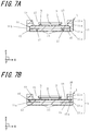
- FIG. 7A is a longitudinal sectional view taken along line A-A of the electronic device shown in FIG. 5A
- FIG. 7B is a longitudinal sectional view taken along line B-B.
- FIG. 8A is a top view showing an electronic device according to a third embodiment
- FIG. 8B is a bottom view of FIG. 8A .
- FIGS. 9A and 9B are internal top views showing the electronic component mounting substrate in the electronic device shown in FIGS. 8A and 8B .
- FIG. 10A is a longitudinal sectional view taken along line A-A of the electronic device shown in FIG. 8A
- FIG. 10B is a longitudinal sectional view taken along line B-B thereof.
- FIG. 11A is a top view showing an electronic device according to a fourth embodiment
- FIG. 11B is a bottom view of FIG. 11A .
- FIGS. 12A and 12B are internal top views of the electronic component mounting substrate in the electronic device shown in FIGS. 11A and 11B .
- FIG. 13A is a longitudinal sectional view taken along line A-A of the electronic device shown in FIG. 11A
- FIG. 13B is a longitudinal sectional view taken along line B-B thereof.
- the electronic device includes an electronic component mounting substrate 1 and an electronic component 2 mounted in a recess 12 of the electronic component mounting substrate 1 .
- the electronic device is connected to a module substrate 4 forming an electronic module using solder 5 , for example.
- the electronic component mounting substrate 1 includes an insulating substrate having a recess 12 that opens in a main surface of the insulating substrate 11 , the recess for mounting an electronic component 2 , a metal layer 13 located on a bottom surface of the recess 12 , an external electrode 14 located on the other main surface of the insulating substrate 11 , the other main surface opposite to the main surface, a connection wiring 15 located between the metal layer 13 and the external electrode 14 in a thickness direction of the insulating substrate 11 .
- the electronic component mounting substrate 1 includes a plurality of first vias 16 connecting the metal layer 13 and the connection wiring 15 and located along a side wall of the recess in a perspective plan view, a plurality of second vias 17 connecting the connection wiring 15 and the external electrode 14 and located in a strip shape in the perspective plan view.
- the upward direction means the positive direction of the virtual z axis. Note that the distinction between the upward and downward directions in the following description is for convenience, and does not limit the upward and downward directions if the electronic component mounting substrate 1 or the like is actually used.
- a portion that overlaps the side wall of the recess 12 and portions that overlap the side surfaces of the second vias 17 are indicated by dotted lines.
- a portion that overlaps the side wall of the recess 12 and regions that overlap the side surfaces of the first vias 16 are indicated by dotted lines.
- a portion that overlaps the side wall of the recess 12 , and portions that overlap the side surfaces of the first vias 16 and the side surfaces of the second vias 17 are indicated by dotted lines.
- the insulating substrate 11 includes a main surface (upper surface in FIGS. 1A to 4 ), the other main surface (lower surface in FIGS. 1A to 4 ) opposite to the main surface, and side surfaces.
- the insulating substrate 11 includes a plurality of insulating layers 11 a , and includes a recess 12 that opens in a main surface of the insulating substrate 11 , the recess for mounting the electronic component 2 .
- the insulating substrate 11 has a rectangular plate shape if viewed from a plan view, that is, from a direction perpendicular to the main surface.
- the insulating substrate 11 serves as a support for supporting the electronic component 2 , and on a mounting portion on the bottom surface of the recess 12 , the electronic component 2 is bonded and fixed through a connection member 3 such as a solder bump, a gold bump, a conductive resin (for example, anisotropic conductive resin), or a resin.
- a connection member 3 such as a solder bump, a gold bump, a conductive resin (for example, anisotropic conductive resin), or a resin.
- the insulating substrate 11 for example, ceramics such as an aluminum oxide sintered body (alumina ceramic), an aluminum nitride sintered body, a silicon nitride sintered body, a mullite sintered body, or a glass ceramic sintered body can be used.
- alumina ceramic aluminum oxide sintered body
- an aluminum nitride sintered body aluminum nitride sintered body
- a silicon nitride sintered body silicon nitride sintered body
- a mullite sintered body a glass ceramic sintered body
- a glass ceramic sintered body for example, ceramics such as an aluminum oxide sintered body (alumina ceramic), an aluminum nitride sintered body, a silicon nitride sintered body, a mullite sintered body, or a glass ceramic sintered body can be used.
- an appropriate organic binder, solvent, and the like are added to and mixed with raw material powders such as aluminum oxide (Al 2 O 3 ), silicon oxide (SiO 2 ),
- a ceramic green sheet is prepared by shaping this slurry into a form of a sheet using a conventionally-known doctor blade method or calender roll method, and the like. Next, an appropriate punching is performed on the ceramic green sheet, a plurality of ceramic green sheets is laminated to form a green body, and the green body is fired at a high temperature (about 1600° C.) to prepare the insulating substrate 11 .
- the recess 12 is located on the main surface of the insulating substrate 11 .
- the recess 12 is for mounting the electronic component 2 on the bottom surface.
- the recess 12 has a rectangular shape with a corner having an arc shape in a plan view, and is disposed in the center portion of the insulating substrate 11 .
- the insulating substrate 11 is formed of four insulating layers 11 a , and the recess 12 is disposed in the first and second insulating layers 11 a from the main surface side of the insulating substrate 11 in the examples illustrated in FIGS. 1A to 3 .
- FIG. 2A and 2B are internal top views of the electronic component mounting substrate 1 in the electronic device.
- FIG. 2A illustrates an upper surface of an insulating layer 11 a that is the third in order from the main surface side of the electronic component mounting substrate 1 , that is, illustrates the bottom surface of the recess 12 .
- FIG. 2B illustrates an upper surface of an insulating layer 11 a that is the fourth in order from the main surface side of the electronic component mounting substrate 1 .
- the recess 12 may be formed by forming through holes to be the recess 12 in the respective ceramic green sheets by laser processing or punching with a mold in a portion of the ceramic green sheets for the insulating substrate 11 , and stacking these ceramic green sheets on the other ceramic green sheet in which no through hole is formed.
- the metal layer 13 , the external electrode 14 , the connection wiring 15 , the first vias 16 , and the second vias 17 are disposed on the surface of, and within the insulating substrate 11 .
- the metal layer 13 , the external electrode 14 , the connection wiring 15 , the first vias 16 , and the second vias 17 are for electrically connecting the electronic component 2 and the module substrate 4 .
- the metal layer 13 is located on the bottom surface of the recess 12 and extends to the lower side of the side wall of the recess 12 , as in the example shown in FIGS. 1A to 3 .
- the external electrode 14 is located on the other main surface of the insulating substrate 11 , as in the example shown in FIGS. 1A to 3 . As in the example shown in FIGS.
- the connection wiring 15 is located between the insulating layers 11 a between the metal layer 13 and the external electrode 14 in the thickness direction of the insulating substrate 11 .
- the first vias 16 and the second vias 17 are located between the bottom surface of the recess 12 and the lower surface of the insulating substrate 11 in the thickness direction of the insulating substrate 11 .
- the second vias 17 are located closer to the other main surface side of the insulating substrate 11 than the first vias 16 .
- the first vias 16 are located along the side wall of the recess 12 and connects the metal layer 13 extending to the lower side of the side wall of the recess 12 and the connection wiring 15 in a perspective plan view.
- the first vias 16 are located in the insulating layer 11 a that is the third in order from the main surface side of the insulating substrate 11 in the example shown in FIGS. 1A to 3 .
- the second vias 17 are located in the insulating layer 11 a that is the fourth in order from the main surface side of the insulating substrate 11 in the example shown in FIGS. 1A to 3 .
- the second vias 17 are located inside the side wall of the recess 12 , that is, located in a region overlapping the recess 12 in a perspective plan view, and connects the external electrode 14 and the connection wiring 15 .
- the second vias 17 are disposed closer to the center than the first vias 16 in a perspective plan view.
- At least two or more first vias 16 are located along the side wall of the recess 12 in a perspective plan view.
- the second vias 17 are located in a strip shape in a perspective plan view as in the example shown in FIGS. 1A to 3 . Note that, being located in a strip shape means that at least three or more second vias 17 are located in a line. In the example shown in FIGS. 1A to 3 , there are six second vias 17 located in the strip shape.
- the metal layer 13 , the external electrode 14 , the connection wiring 15 , the first vias 16 , and the second vias 17 are metallization of a metal powder having a main component of tungsten (W), molybdenum (Mo), manganese (Mn), silver (Ag), copper (Cu), and the like, for example.
- the insulating substrate 11 is made of an aluminum oxide sintered body
- a metallized paste obtained by adding and mixing a suitable organic binder, solvent, and the like to a refractory metal powder such as W, Mo or Mn is preliminarily printed and applied in a predetermined pattern on the ceramic green sheet for the insulating substrate 11 by a screen printing method, and is fired at the same time as the ceramic green sheet for the insulating substrate 11 , to be deposited on a predetermined position of the insulating substrate 11 .
- the metal layer 13 , the external electrode 14 and the connection wiring 15 are formed by printing and applying the metallized paste for the metal layer 13 , the external electrode 14 , and the connection wiring 15 , on a ceramic green sheet for the insulating substrate 11 by a printing means such as a screen printing method, and firing the result together with the ceramic green sheet for the insulating substrate 11 .
- the first vias 16 and the second vias 17 are formed by forming through holes for a through conductor in a ceramic green sheet for the insulating substrate 11 by the processing method such as punching with mold, or laser processing, and filling the through hole with the metallized paste for the first vias 16 and the second vias 17 by the printing means, and firing the result together with the ceramic green sheet for the insulating substrate 11 .
- the metallized paste is prepared by adjusting the viscosity to an appropriate level by adding a suitable solvent and binder to the metal powder described above and kneading the same.
- glass powder or ceramic powder may be included.
- a metal plating layer is deposited on a surface of the metal layer 13 and the external electrode 14 exposed from the insulating substrate 11 by electroplating or electroless plating.
- the metal plating layer is formed of a metal having good corrosion resistance and connection member connectivity, such as nickel, copper, gold, or silver, and is sequentially deposited with a nickel plating layer having a thickness of about 0.5 to 5 ⁇ m and a gold plating layer having a thickness of about 0.1 to 3 ⁇ m, for example.
- the corrosion of the metal layer 13 and the external electrode 14 can be effectively suppressed, and the bonding between the electronic component 2 and the metal layer 13 , the bonding between the metal layer 13 and the connection member 3 such as a bonding wire, and the bonding between the external electrode 14 and the connection pad 41 for connection on the module substrate 4 can be strengthened.
- the metal plating layer is not limited to the nickel plating layer/gold plating layer, and may be other metal plating layers including nickel plating layer/palladium plating layer/gold plating layer.
- An electronic device can be prepared by mounting the electronic component 2 on the bottom surface of the recess 12 of the electronic component mounting substrate 1 .
- the electronic component 2 mounted on the electronic component mounting substrate 1 is, for example, a semiconductor element such as an IC chip or an LSI chip, a light emitting element, a piezoelectric element such as a crystal oscillator or a piezoelectric vibrator, and various sensors.
- the electronic component 2 is a wire bonding type semiconductor element
- the semiconductor element is fixed to the bottom surface of the recess 12 by a bonding member such as a low melting point brazing material or a conductive resin, and then mounted on the electronic component mounting substrate 1 by electrically connecting the electrode of the semiconductor element and the metal layer 13 through the connection member 3 such as a bonding wire.
- the electronic component 2 is electrically connected to the metal layer 13 .
- the semiconductor element is mounted on the electronic component mounting substrate 1 by electrically and mechanically connecting the electrode and the metal layer 13 of the semiconductor element through the connection member 3 such as a solder bump, a gold bump, or a conductive resin (anisotropic conductive resin and the like).
- the connection member 3 such as a solder bump, a gold bump, or a conductive resin (anisotropic conductive resin and the like).
- a plurality of electronic components 2 may be mounted, or a small electronic component such as a resistor element or a capacitor element may be mounted as necessary.
- the electronic component 2 is sealed using a sealing material made of resin, glass, and the like, or by a cover made of resin, glass, ceramics, metal, and the like, as necessary.
- the external electrodes 14 of the electronic device according to the present embodiment are connected to the connection pads 41 of the module substrate through the solder 5 to form an electronic module.
- the external electrodes 14 arranged on the other main surface of the electronic component mounting substrate 1 are connected to the connection pads 41 of the module substrate 4 .
- the electronic component mounting substrate 1 includes the insulating substrate 11 having a recess 12 that opens in a main surface of the insulating substrate 11 , the recess for mounting an electronic component 2 , the metal layer 13 located on a bottom surface of the recess 12 , the external electrode 14 located on the other main surface of the insulating substrate 11 , the other main surface opposite to the main surface, the connection wiring 15 located between the metal layer 13 and the external electrode 14 in a thickness direction of the insulating substrate 11 , a plurality of first vias 16 that connects the metal layer 13 and the connection wiring 15 and that is located along a side wall of the recess 12 in a perspective plan view, and a plurality of second vias 17 that connects the connection wiring 15 and the external electrode 14 and that is located in a strip shape in the perspective plan view.
- a plurality of first vias 16 located on the bottom surface side of the recess 12 is located on an outer periphery side of the recess 12 overlapping the side wall
- a plurality of second vias 17 located on the other main surface side and connected to the external electrode 14 is located inward the recess 12 relative to the plurality of first vias 16 , and thus a plurality of vias is separately located on the bottom surface side of the recess and the lower surface side of the insulating substrate 11 .
- the heat sources in the plurality of first vias 16 and the plurality of second vias 17 are separated, and thus the heat generated by the plurality of second vias 17 connected to the external electrode 14 is generated in the vicinity of the center of the insulating substrate 11 and spreads over the entire external electrode 14 along the arrangement of the plurality of second vias 17 to be easily dissipated to the outside.
- a high current is applied to the plurality of first vias 16 and the plurality of second vias 17 , it is possible to reduce stress generated at the outer edge (side surface and lower side surface) of the insulating substrate 11 along the vias and to reduce occurrence of distortion in the insulating substrate 11 .
- the electronic component mounting substrate 1 for a light emitting device having good luminance can be employed.
- the plurality of first vias 16 and the plurality of the second vias 17 are located in the insulating substrate 11 , and thus heat generation of the individual via is reduced by suppressing the current applied to an individual via through the metal layer 13 or the external electrode 14 . Because there is a plurality of second vias 17 located in a strip shape as in the example shown in FIGS. 1A to 2B , the heat generated by the second vias 17 may be dissipated to the external electrode 14 in the strip shape, and dispersed to the external electrode 14 to facilitate heat transfer, and the heat transfer from the external electrode 14 to the module substrate 4 may be improved, thus resulting in reduced occurrence of distortion in the insulating substrate 11 .
- the plurality of first vias 16 and the plurality of second vias 17 are connected to one connection wiring 15 as in the example shown in FIG. 2B .
- the plurality of first vias 16 is connected to one connection wiring 15 as in the example shown in FIGS. 2A and 2B . If the plurality of first vias 16 overlaps the outer edge of the connection wiring 15 in a perspective plan view, the plurality of first vias 16 is connected to the outer edge of one connection wiring 15 , and thus the heat of the plurality of first vias 16 is dispersed in the vicinity of the outer edge of the insulating substrate 11 to facilitate heat dissipation. In addition, the variation in the current value applied to each of the plurality of first vias 16 via one connection wiring 15 is reduced, the occurrence of large heat generation in each of the plurality of first vias 16 is reduced, and thus it is possible to reduce occurrence of distortion in the insulating substrate 11 .
- first vias 16 and the plurality of second vias 17 are disposed without overlapping the electronic component 2 in a perspective plan view as shown in the examples shown in FIGS. 1A to 4 , heat transfer from the electronic component 2 to the first vias 16 and the second vias 17 may be suppressed, and deterioration of the heat generation of the first vias 16 and heat generation of the second vias 17 may be suppressed, thus resulting in reduced occurrence of distortion in the insulating substrate 11 .
- connection wirings 15 are located opposite to each other with the mounting portion of the electronic component 2 being interposed therebetween, the variation in the current value applied to each of the plurality of first vias 16 in the opposite directions is reduced, and the occurrence of large heat generation in each of the plurality of first vias 16 is reduced, thus resulting in reduced occurrence of distortion in the insulating substrate 11 .
- the electronic device includes the electronic component mounting substrate 1 having the configuration described above and the electronic component 2 mounted in the recess 12 of the electronic component mounting substrate 1 , and as a result, an electronic device with increased long-term reliability can be obtained.
- the electronic module according to the present embodiment includes the module substrate 4 having the connection pads 41 , and the electronic device having the configuration described above connected to the external electrode 14 through the solder on the connection pad 41 , thereby providing the increased long-term reliability.
- the electronic component mounting substrate 1 can be suitably used in a small and high-power electronic device.
- a light emitting element such as an LED
- the electronic component mounting substrate 1 may be suitably used for a thin and high-luminance light emitting device.
- the electronic device according to the second embodiment is different from the electronic device according to the embodiment described above in that a notch 11 b is disposed in a side surface of the insulating substrate 11 , and the connection wiring 15 includes a protrusion 15 a protruding to the side surface where the notch 11 b is located in a perspective plan view.
- the insulating substrate 11 is formed of four insulating layers 11 a
- the recess 12 is disposed in the first and second insulating layers 11 a of the upper surface side of the insulating substrate 11 in the examples illustrated in FIGS. 5A to 7B .
- FIGS. 6A and 6B are internal top views of the electronic component mounting substrate 1 in the electronic device.
- FIG. 6A illustrates an upper surface of the insulating layer 11 a that is the third in order from the main surface side of the electronic component mounting substrate 1 , that is, illustrates a bottom surface of the recess 12 .
- FIG. 6B illustrates an upper surface of the insulating layer 11 a that is the fourth in order from the main surface side of the electronic component mounting substrate 1 .
- a portion that overlaps the inner wall of the recess 12 and portions that overlap the side surfaces of the second vias 17 are indicated by dotted lines.
- a portion that overlaps the inner wall of the recess 12 and portions that overlap the side surfaces of the first vias 16 are indicated by dotted lines.
- a portion that overlaps the inner wall of the recess 12 , and portions that overlap the side surfaces of the first vias 16 and the side surfaces of the second vias 17 are indicated by dotted lines.
- a plurality of first vias 16 located on the bottom surface side of the recess 12 is located on the outer periphery side of the recess 12 overlapping the side wall
- a plurality of second vias 17 located on the other main surface side and connected to the external electrode 14 is located further inward the recess 12 than the plurality of first vias 16 , and thus a plurality of vias is separately arranged on the bottom surface side of the recess 12 and the lower surface side of the insulating substrate 11 .
- the heat sources in the plurality of first vias 16 and the plurality of second vias 17 are separated, and thus the heat generated by the plurality of second vias 17 connected to the external electrode 14 is generated in the vicinity of the center of the insulating substrate 11 and spreads over the entire external electrode 14 along the arrangement of the plurality of second vias 17 to be easily dissipated to the outside.
- a high current is applied to the plurality of first vias 16 and the plurality of second vias 17 , it is possible to reduce stress generated at the outer edge (side surface and lower side surface) of the insulating substrate 11 along the vias and to reduce occurrence of distortion in the insulating substrate 11 .
- connection wiring 15 includes a protrusion 15 a protruding to the side surface where the notch 11 b is located. Accordingly, the heat transferred to the connection wiring 15 from the plurality of first vias 16 is dispersed and easily dissipated to the notch 11 b side, and thus it is possible to reduce occurrence of distortion in the insulating substrate 11 .
- the plurality of first vias 16 overlaps the protrusions 15 a in a perspective plan view, the plurality of first vias 16 is connected to the protrusions 15 a of one connection wiring 15 , and thus the heat of the plurality of first vias 16 may be dispersed in the vicinity of the notch 11 b of the insulating substrate 11 and may be easily dissipated to the notch 11 b . As a result, the occurrence of distortion in the insulating substrate 11 may be reduced.
- the notch 11 b is located in the side surface of the insulating substrate 11 in the thickness direction of the insulating substrate 11 .
- one notch 11 b is located in each of two opposite to side surfaces of the insulating substrate 11 .
- the notch 11 b is located in the insulating layer 11 a between the bottom surface of the recess 12 and the other main surface of the insulating substrate 11 , but may penetrate the insulating substrate 11 in the thickness direction.
- the notch 11 b may be manufactured by the same method as that for the recess 12 described above. For example, it may be formed by forming through holes to be the notch 11 b in the respective ceramic green sheets by laser processing or punching with a mold in a portion of the ceramic green sheets for the insulating substrate 11 and by stacking these ceramic green sheets on another ceramic green sheet in which no through hole is formed.
- a side conductor 18 is disposed on an inner surface of the notch 11 b .
- the end of the side conductor 18 is connected to the external electrode 14 , and may be connected to the connection pad 41 of the module substrate 4 through the solder 5 together with the external electrode 14 .
- connection wiring 15 includes the protrusion 15 a protruding to the side surface where the notch 11 b is located and the solder 5 is connected to the side conductor 18 of the notch 11 b
- the heat of the plurality of first vias 16 may be dispersed in the vicinity of the notch 11 b of the insulating substrate 11 to be easily dissipated to the notch 11 b where the side conductor 18 and the solder 5 are disposed, thus resulting in reduced occurrence of distortion in the insulating substrate 11 .
- the side conductor 18 may be formed by the same material and method as the metal layer 13 , the external electrode 14 and the connection wiring 15 described above. For example, it is formed by applying by printing a metallized paste for the side conductor 18 onto the through hole for the notch 11 b disposed in the ceramic green sheet for the insulating substrate 11 , by a printing means such as a screen printing method, and firing the result together with a ceramic green sheet for the insulating substrate 11 .
- a metal plating layer is disposed on the exposed surface of the side conductor 18 to strengthen the connection with the connection pad 41 for connection purpose formed on the module substrate 4 together with the external electrode 14 .
- two (a pair) of the plurality of first vias 16 are arranged respectively in two protrusions 15 a (two regions) located with the notch 11 b being interposed therebetween.
- the number of the first vias 16 located in the respective regions of the two protrusions 15 a may be the same as each other, and the currents applied to the respective regions of the two protrusions 15 a , that is, to the respective protrusions 15 a and the plurality of first vias 16 , are equally distributed.
- the protrusions 15 a are located with the notch 11 b being interposed therebetween. Accordingly, the heat generated by the plurality of first vias 16 and the connection wiring is well dispersed to the notch 11 b , and thus it is possible to reduce occurrence of distortion in the insulating substrate 11 .
- the interval between each of the two protrusions 15 a (two regions) and the notch 11 b may be formed by an equal interval within a range of 10%.
- connection wiring 15 and the protrusion 15 a are located opposite to each other with the mounting portion of the electronic component 2 being interposed therebetween, the variation in the current value applied to each of the plurality of first vias 16 in the opposite directions is reduced, and the occurrence of large heat generation in each of the plurality of first vias 16 is reduced, thus resulting in reduced occurrence of distortion in the insulating substrate 11 .
- the plurality of first vias 16 and the plurality of second vias 17 are located without overlapping the electronic component 2 in a perspective plan view as shown in the examples shown in FIGS. 5A to 7B , like the electronic component mounting substrate 1 according to the first embodiment, heat transfer from the electronic component 2 to the first vias 16 and the second vias 17 may be suppressed, and deterioration of the heat generation of the first vias 16 and heat generation of the second vias 17 may be suppressed, thus resulting in reduced occurrence of distortion in the insulating substrate 11 .
- the electronic component mounting substrate 1 according to the second embodiment may be manufactured using the same manufacturing method as the electronic component mounting substrate 1 according to the embodiment described above.
- FIGS. 8A to 10B an electronic device according to a third embodiment will be described with reference to FIGS. 8A to 10B .
- the electronic device according to the third embodiment is different from the electronic device according to the embodiment described above in that the plurality of first vias 16 is located to surround the plurality of second vias 17 in a perspective plan view.
- the insulating substrate 11 is formed of four insulating layers 11 a
- the recess 12 is located in the first and second insulating layers 11 a of the upper surface side of the insulating substrate 11 in the examples illustrated in FIGS. 8A to 10B .
- FIGS. 9A and 9B are internal top views of the electronic component mounting substrate 1 in the electronic device.
- FIG. 9A and 9B are internal top views of the electronic component mounting substrate 1 in the electronic device.
- FIG. 9A illustrates an upper surface of the insulating layer 11 a that is the third in order from the electronic component mounting substrate 1 , that is, illustrates the bottom surface of the recess 12 .
- FIG. 9B illustrates an upper surface of the insulating layer 11 a that is the fourth in order from the electronic component mounting substrate 1 .
- a portion that overlaps the inner wall of the recess 12 and portions that overlap the side surfaces of the second vias 17 are indicated by dotted lines.
- a portion that overlaps the inner wall of the recess 12 and portions that overlap the side surfaces of the first vias 16 are indicated by dotted lines.
- a portion that overlaps the inner wall of the recess 12 , and portions that overlap the side surfaces of the first vias 16 and the side surfaces of the second vias 17 are indicated by dotted lines.
- a plurality of first vias 16 located on the bottom surface side of the recess 12 is located on the outer periphery side of the recess 12 overlapping the side wall
- a plurality of second vias 17 located on the other main surface side and connected to the external electrode 14 is located further inward the recess 12 than the plurality of first vias 16 , and thus a plurality of vias is separately located on the bottom surface side of the recess 12 and the lower surface side of the insulating substrate 11 .
- the heat sources in the plurality of first vias 16 and the plurality of second vias 17 are separated, and thus the heat generated by the plurality of second vias 17 connected to the external electrode 14 is generated in the vicinity of the center of the insulating substrate 11 and spreads over the entire external electrode 14 along the arrangement of the plurality of second vias 17 to be easily dissipated to the outside.
- a high current is applied to the plurality of first vias 16 and the plurality of second vias 17 , it is possible to reduce stress generated at the outer edge (side surface and lower side surface) of the insulating substrate 11 along the vias and to reduce occurrence of distortion in the insulating substrate 11 .
- the electronic component mounting substrate 1 for a light emitting device having good luminance can be employed.
- the plurality of first vias 16 surrounds the plurality of second vias 17 . Accordingly, the current is distributed to the plurality of first vias 16 through the metal layer 13 or the connection wiring 15 , and thus stress applied to the first vias 16 is dispersed in multiple directions. As a result, even if a high current is applied to the first vias 16 and the second vias 17 , it is possible to reduce occurrence of distortion in the insulating substrate 11 .
- two (a pair) of the plurality of first vias 16 are respectively located on three sides (three regions) of the insulating substrate 11 . If there are equal number of first vias 16 located in each region of the three sides (three regions) of the insulating substrate 11 , even if a high current is applied to the first vias 16 and the second vias 17 , it is evenly distributed in the three regions, thus resulting in reduced occurrence of distortion in the insulating substrate 11 .
- connection wiring 15 and the protrusion 15 a are located opposite to each other with the mounting portion of the electronic component 2 being interposed therebetween, the variation in the current value applied to each of the plurality of first vias 16 in the opposite directions is reduced, and the occurrence of large heat generation in each of the plurality of first vias 16 is reduced, thus resulting in reduced occurrence of distortion in the insulating substrate 11 .
- a plurality of first vias 16 and second vias 17 are connected to one connection wiring 15 disposed between the insulating layers.
- the number of the plurality of first vias 16 is greater than the number of the plurality of second vias 17 , the number of first vias 16 closer to the electronic component 2 is increased, the heat generation from individual vias is reduced, and thus the overall stress applied to the vias is distributed. As a result, even if a high current is applied to the first vias 16 and the second vias 17 , the occurrence of distortion in the insulating substrate 11 may be reduced.
- the total area of the plurality of first vias 16 is smaller than the total area of the plurality of second vias 17 , the area of first vias 16 closer to the electronic component 2 is increased, and thus the heat generation from the individual vias is reduced and the overall stress applied to the vias is distributed. As a result, even if a high current is applied to the first vias 16 and the second vias 17 , the occurrence of distortion in the insulating substrate 11 may be reduced.
- the plurality of first vias 16 and the plurality of second vias 17 are located without overlapping the electronic component 2 in a perspective plan view as shown in the examples shown in FIGS. 8A to 10B , like the electronic component mounting substrate 1 according to the first embodiment, heat transfer from the electronic component 2 to the first vias 16 and the second vias 17 may be suppressed, and deterioration of the heat generation of the first vias 16 and heat generation of the second vias 17 may be suppressed, thus resulting in reduced occurrence of distortion in the insulating substrate 11 .
- the electronic component mounting substrate 1 according to the third embodiment may be manufactured using the same manufacturing method as the electronic component mounting substrate 1 according to the embodiment described above.
- FIGS. 11A to 13B an electronic device according to a fourth embodiment will be described with reference to FIGS. 11A to 13B .
- the electronic device according to the fourth embodiment is different from the electronic device according to the embodiment described above in that the recess 12 is circular in a perspective plan view.
- the insulating substrate 11 is formed of four insulating layers 11 a
- the recess 12 is located in the first and second insulating layers 11 a of the upper surface side of the insulating substrate 11 in the examples illustrated in FIGS. 11A to 13B .
- FIGS. 12A and 12B are internal top views of the electronic component mounting substrate 1 in the electronic device.
- FIG. 12A illustrates an upper surface of the insulating layer 11 a that is the third in order from the electronic component mounting substrate 1 , that is, illustrates the bottom surface of the recess 12 .
- FIG. 12B illustrates an upper surface of the insulating layer 11 a that is the fourth in order from the electronic component mounting substrate 1 .
- a portion that overlaps the inner wall of the recess 12 and portions that overlap the side surfaces of the second vias 17 are indicated by dotted lines.
- a portion that overlaps the inner wall of the recess 12 and portions that overlap the side surfaces of the first vias 16 are indicated by dotted lines.
- a portion that overlaps the inner wall of the recess 12 , and portions that overlap the side surfaces of the first vias 16 and the side surfaces of the second vias 17 are indicated by dotted lines.
- a plurality of first vias 16 located on the bottom surface side of the recess 12 is located on the outer periphery side of the recess 12 overlapping the side wall
- a plurality of second vias 17 located on the other main surface side and connected to the external electrode 14 is located further inward the recess 12 than the plurality of first vias 16 , and thus a plurality of vias is separately located on the bottom surface side of the recess 12 and the lower surface side of the insulating substrate 11 .
- the heat sources in the plurality of first vias 16 and the plurality of second vias 17 are separated, and thus the heat generated by the plurality of second vias 17 connected to the external electrode 14 is generated in the vicinity of the center of the insulating substrate 11 and spreads over the entire external electrode 14 along the arrangement of the plurality of second vias 17 to be easily dissipated to the outside.
- a high current is applied to the plurality of first vias 16 and the plurality of second vias 17 , it is possible to reduce stress generated at the outer edge (side surface and lower side surface) of the insulating substrate 11 along the vias and to reduce occurrence of distortion in the insulating substrate 11 .
- the electronic component mounting substrate 1 for a light emitting device having good luminance can be employed.
- the plurality of first vias 16 is located along the side wall of the circular recess 12 in a perspective plan view.
- connection wiring 15 and the protrusion 15 a are located opposite to each other with the mounting portion of the electronic component 2 being interposed therebetween, the variation in the current value applied to each of the plurality of first vias 16 in the opposite directions is reduced, and the occurrence of large heat generation in each of the plurality of first vias 16 is reduced, thus resulting in reduced occurrence of distortion in the insulating substrate 11 .
- the external electrode 14 includes three external electrodes 14 in the examples shown in FIGS. 11A to 13B .
- the two external electrodes 14 located on the outer side are connected to the plurality of second vias 17 , respectively.
- the external electrode 14 located closer to the center may be electrically connected to one of the other two external electrodes 14 located on the outer side and disposed with the plurality of second vias 17 .
- the plurality of first vias 16 and the plurality of second vias 17 are located without overlapping the electronic component 2 in a perspective plan view as shown in the examples shown in FIGS. 11A to 13B , like the electronic component mounting substrate 1 , heat transfer from the electronic component 2 to the first vias 16 and the second vias 17 may be suppressed, and deterioration of the heat generation of the first vias 16 and heat generation of the second vias 17 may be suppressed, thus resulting in reduced occurrence of distortion in the insulating substrate 11 .
- the electronic component mounting substrate 1 according to the fourth embodiment may be manufactured using the same manufacturing method as the electronic component mounting substrate 1 according to the embodiment described above.
- the insulating substrate 11 may have a rectangular shape having the notch 11 b or a chamfered portion in a side surface or a corner thereof in a plan view.
- the side wall surface of the recess 12 may be perpendicular to the bottom surface of the recess 12 in a longitudinal sectional view
- the side wall surface of the recess 12 may be an inclined surface so that the opening of the recess 12 is wider than the bottom surface of the recess 12 .
- a reflective layer may be located on the side wall surface of the recess 12 .
- a light emitting element is used as the electronic component 2
- it may be suitably used as the electronic component mounting substrate 1 for a light emitting device having good light emission luminance by positioning a reflective layer with good reflectivity on the side wall surface of the recess 12 .
- the electronic component mounting substrates 1 according to the first to fourth embodiments may be combined with each other.
- the recess 12 may be circular in a plan view.
- the examples are shown in which the insulating substrate 11 is formed of the four insulating layers 11 a , but the insulating substrate 11 may be formed of three, or five or more insulating layers 11 a.
- the electronic component mounting substrate 1 may be manufactured in the form of a multi-piece electronic component mounting substrate.
Abstract
Description
Claims (7)
Applications Claiming Priority (4)
| Application Number | Priority Date | Filing Date | Title |
|---|---|---|---|
| JP2017-104725 | 2017-05-26 | ||
| JPJP2017-104725 | 2017-05-26 | ||
| JP2017104725 | 2017-05-26 | ||
| PCT/JP2018/020170 WO2018216801A1 (en) | 2017-05-26 | 2018-05-25 | Electronic component mounting substrate, electronic device, and electronic module |
Publications (2)
| Publication Number | Publication Date |
|---|---|
| US20200105658A1 US20200105658A1 (en) | 2020-04-02 |
| US11145587B2 true US11145587B2 (en) | 2021-10-12 |
Family
ID=64395599
Family Applications (1)
| Application Number | Title | Priority Date | Filing Date |
|---|---|---|---|
| US16/614,927 Active US11145587B2 (en) | 2017-05-26 | 2018-05-25 | Electronic component mounting substrate, electronic device, and electronic module |
Country Status (5)
| Country | Link |
|---|---|
| US (1) | US11145587B2 (en) |
| EP (1) | EP3633719A4 (en) |
| JP (1) | JP6748302B2 (en) |
| CN (1) | CN110622300B (en) |
| WO (1) | WO2018216801A1 (en) |
Cited By (1)
| Publication number | Priority date | Publication date | Assignee | Title |
|---|---|---|---|---|
| US20210272868A1 (en) * | 2018-06-26 | 2021-09-02 | Kyocera Corporation | Electronic element mounting substrate, electronic device, and electronic module |
Families Citing this family (4)
| Publication number | Priority date | Publication date | Assignee | Title |
|---|---|---|---|---|
| CN109997220B (en) * | 2016-11-28 | 2023-09-12 | 京瓷株式会社 | Wiring substrate, electronic device, and electronic module |
| JP7136926B2 (en) * | 2018-12-26 | 2022-09-13 | 京セラ株式会社 | Wiring boards, electronic devices and electronic modules |
| JP7449768B2 (en) * | 2020-04-23 | 2024-03-14 | 新光電気工業株式会社 | Ceramic substrates and their manufacturing methods, electrostatic chucks, substrate fixing devices, packages for semiconductor devices |
| JP7368771B2 (en) | 2021-09-30 | 2023-10-25 | 日亜化学工業株式会社 | Light emitting device, linear light source and driving method thereof |
Citations (6)
| Publication number | Priority date | Publication date | Assignee | Title |
|---|---|---|---|---|
| JP2008130946A (en) | 2006-11-24 | 2008-06-05 | Ngk Spark Plug Co Ltd | Multiple patterning ceramic substrate, and ceramic wiring substrate and method of manufacturing the same |
| US20130049564A1 (en) | 2011-08-22 | 2013-02-28 | Su Jung JUNG | Light emitting device package and light unit |
| US20150146397A1 (en) * | 2012-05-30 | 2015-05-28 | Kyocera Corporation | Wiring board and electronic device |
| JP2015159245A (en) | 2014-02-25 | 2015-09-03 | 京セラ株式会社 | Package for mounting light-emitting element and light-emitting device |
| US20150305160A1 (en) * | 2013-01-22 | 2015-10-22 | Kyocera Corporation | Package for mounting electronic element, electronic device, and imaging module |
| US9704791B2 (en) * | 2013-10-23 | 2017-07-11 | Kyocera Corporation | Wiring board and electronic device |
Family Cites Families (8)
| Publication number | Priority date | Publication date | Assignee | Title |
|---|---|---|---|---|
| DE112010002822T5 (en) * | 2009-07-03 | 2012-06-14 | Seoul Semiconductor Co., Ltd. | HOUSING FOR LIGHT EMITTING DIODES |
| JP5770006B2 (en) * | 2011-04-15 | 2015-08-26 | シチズン電子株式会社 | Semiconductor light emitting device |
| US8773006B2 (en) * | 2011-08-22 | 2014-07-08 | Lg Innotek Co., Ltd. | Light emitting device package, light source module, and lighting system including the same |
| JP6400928B2 (en) * | 2014-03-26 | 2018-10-03 | 京セラ株式会社 | Wiring board and electronic device |
| CN106463470B (en) * | 2014-07-29 | 2019-04-05 | 京瓷株式会社 | Circuit board, electronic device and electronic module |
| JP6267803B2 (en) * | 2014-09-26 | 2018-01-24 | 京セラ株式会社 | Wiring board, electronic device and electronic module |
| CN206059386U (en) * | 2015-04-01 | 2017-03-29 | 三菱电机株式会社 | Circuit board and electronic installation |
| JP6698301B2 (en) * | 2015-09-24 | 2020-05-27 | 京セラ株式会社 | Wiring board, electronic device and electronic module |
-
2018
- 2018-05-25 EP EP18804931.6A patent/EP3633719A4/en active Pending
- 2018-05-25 CN CN201880031796.3A patent/CN110622300B/en active Active
- 2018-05-25 JP JP2019520327A patent/JP6748302B2/en active Active
- 2018-05-25 WO PCT/JP2018/020170 patent/WO2018216801A1/en active Application Filing
- 2018-05-25 US US16/614,927 patent/US11145587B2/en active Active
Patent Citations (6)
| Publication number | Priority date | Publication date | Assignee | Title |
|---|---|---|---|---|
| JP2008130946A (en) | 2006-11-24 | 2008-06-05 | Ngk Spark Plug Co Ltd | Multiple patterning ceramic substrate, and ceramic wiring substrate and method of manufacturing the same |
| US20130049564A1 (en) | 2011-08-22 | 2013-02-28 | Su Jung JUNG | Light emitting device package and light unit |
| US20150146397A1 (en) * | 2012-05-30 | 2015-05-28 | Kyocera Corporation | Wiring board and electronic device |
| US20150305160A1 (en) * | 2013-01-22 | 2015-10-22 | Kyocera Corporation | Package for mounting electronic element, electronic device, and imaging module |
| US9704791B2 (en) * | 2013-10-23 | 2017-07-11 | Kyocera Corporation | Wiring board and electronic device |
| JP2015159245A (en) | 2014-02-25 | 2015-09-03 | 京セラ株式会社 | Package for mounting light-emitting element and light-emitting device |
Cited By (1)
| Publication number | Priority date | Publication date | Assignee | Title |
|---|---|---|---|---|
| US20210272868A1 (en) * | 2018-06-26 | 2021-09-02 | Kyocera Corporation | Electronic element mounting substrate, electronic device, and electronic module |
Also Published As
| Publication number | Publication date |
|---|---|
| US20200105658A1 (en) | 2020-04-02 |
| EP3633719A4 (en) | 2021-03-17 |
| CN110622300A (en) | 2019-12-27 |
| JP6748302B2 (en) | 2020-08-26 |
| JPWO2018216801A1 (en) | 2020-03-19 |
| CN110622300B (en) | 2024-03-12 |
| WO2018216801A1 (en) | 2018-11-29 |
| EP3633719A1 (en) | 2020-04-08 |
Similar Documents
| Publication | Publication Date | Title |
|---|---|---|
| US11145587B2 (en) | Electronic component mounting substrate, electronic device, and electronic module | |
| WO2020045480A1 (en) | Wiring board, electronic device and electronic module | |
| JP6791719B2 (en) | Substrate for mounting electronic components, electronic devices and electronic modules | |
| US10249564B2 (en) | Electronic component mounting substrate, electronic device, and electronic module | |
| JP6698826B2 (en) | Substrate for mounting electronic parts, electronic device and electronic module | |
| JP2023071984A (en) | Wiring board, electronic device, and electronic module | |
| JP6626735B2 (en) | Electronic component mounting board, electronic device and electronic module | |
| US11004781B2 (en) | Electronic component mounting substrate, electronic device, and electronic module | |
| JP6698301B2 (en) | Wiring board, electronic device and electronic module | |
| WO2017073486A1 (en) | Wiring substrate, electronic device and electronic module | |
| US10937707B2 (en) | Wiring substrate, electronic device, and electronic module | |
| WO2018155434A1 (en) | Wiring substrate, electronic device, and electronic module | |
| JP6737646B2 (en) | Wiring board, electronic device and electronic module | |
| JP2015159139A (en) | Wiring board, electronic apparatus, and electronic module | |
| JP6595308B2 (en) | Electronic component mounting substrate, electronic device and electronic module | |
| JP2017112270A (en) | Substrate for mounting electronic component, electronic device and electronic module |
Legal Events
| Date | Code | Title | Description |
|---|---|---|---|
| FEPP | Fee payment procedure |
Free format text: ENTITY STATUS SET TO UNDISCOUNTED (ORIGINAL EVENT CODE: BIG.); ENTITY STATUS OF PATENT OWNER: LARGE ENTITY |
|
| AS | Assignment |
Owner name: KYOCERA CORPORATION, JAPAN Free format text: ASSIGNMENT OF ASSIGNORS INTEREST;ASSIGNORS:BABA, YUUKI;MORIYAMA, YOUSUKE;REEL/FRAME:051059/0656 Effective date: 20180629 |
|
| STPP | Information on status: patent application and granting procedure in general |
Free format text: NON FINAL ACTION MAILED |
|
| STPP | Information on status: patent application and granting procedure in general |
Free format text: NON FINAL ACTION MAILED |
|
| STPP | Information on status: patent application and granting procedure in general |
Free format text: RESPONSE TO NON-FINAL OFFICE ACTION ENTERED AND FORWARDED TO EXAMINER |
|
| STPP | Information on status: patent application and granting procedure in general |
Free format text: NOTICE OF ALLOWANCE MAILED -- APPLICATION RECEIVED IN OFFICE OF PUBLICATIONS |
|
| STPP | Information on status: patent application and granting procedure in general |
Free format text: AWAITING TC RESP., ISSUE FEE NOT PAID |
|
| STPP | Information on status: patent application and granting procedure in general |
Free format text: NOTICE OF ALLOWANCE MAILED -- APPLICATION RECEIVED IN OFFICE OF PUBLICATIONS |
|
| STPP | Information on status: patent application and granting procedure in general |
Free format text: PUBLICATIONS -- ISSUE FEE PAYMENT RECEIVED |
|
| STPP | Information on status: patent application and granting procedure in general |
Free format text: PUBLICATIONS -- ISSUE FEE PAYMENT VERIFIED |
|
| STCF | Information on status: patent grant |
Free format text: PATENTED CASE |