US11088129B2 - Display apparatus - Google Patents
Display apparatus Download PDFInfo
- Publication number
- US11088129B2 US11088129B2 US16/502,046 US201916502046A US11088129B2 US 11088129 B2 US11088129 B2 US 11088129B2 US 201916502046 A US201916502046 A US 201916502046A US 11088129 B2 US11088129 B2 US 11088129B2
- Authority
- US
- United States
- Prior art keywords
- circuit layer
- layer
- disposed
- thin
- film transistor
- Prior art date
- Legal status (The legal status is an assumption and is not a legal conclusion. Google has not performed a legal analysis and makes no representation as to the accuracy of the status listed.)
- Active, expires
Links
Images


Classifications
-
- H—ELECTRICITY
- H10—SEMICONDUCTOR DEVICES; ELECTRIC SOLID-STATE DEVICES NOT OTHERWISE PROVIDED FOR
- H10D—INORGANIC ELECTRIC SEMICONDUCTOR DEVICES
- H10D86/00—Integrated devices formed in or on insulating or conducting substrates, e.g. formed in silicon-on-insulator [SOI] substrates or on stainless steel or glass substrates
- H10D86/40—Integrated devices formed in or on insulating or conducting substrates, e.g. formed in silicon-on-insulator [SOI] substrates or on stainless steel or glass substrates characterised by multiple TFTs
- H10D86/441—Interconnections, e.g. scanning lines
- H10D86/443—Interconnections, e.g. scanning lines adapted for preventing breakage, peeling or short circuiting
-
- H01L25/18—
-
- H—ELECTRICITY
- H10—SEMICONDUCTOR DEVICES; ELECTRIC SOLID-STATE DEVICES NOT OTHERWISE PROVIDED FOR
- H10W—GENERIC PACKAGES, INTERCONNECTIONS, CONNECTORS OR OTHER CONSTRUCTIONAL DETAILS OF DEVICES COVERED BY CLASS H10
- H10W90/00—Package configurations
-
- G—PHYSICS
- G06—COMPUTING OR CALCULATING; COUNTING
- G06F—ELECTRIC DIGITAL DATA PROCESSING
- G06F3/00—Input arrangements for transferring data to be processed into a form capable of being handled by the computer; Output arrangements for transferring data from processing unit to output unit, e.g. interface arrangements
- G06F3/01—Input arrangements or combined input and output arrangements for interaction between user and computer
- G06F3/03—Arrangements for converting the position or the displacement of a member into a coded form
- G06F3/041—Digitisers, e.g. for touch screens or touch pads, characterised by the transducing means
- G06F3/044—Digitisers, e.g. for touch screens or touch pads, characterised by the transducing means by capacitive means
- G06F3/0445—Digitisers, e.g. for touch screens or touch pads, characterised by the transducing means by capacitive means using two or more layers of sensing electrodes, e.g. using two layers of electrodes separated by a dielectric layer
-
- G—PHYSICS
- G06—COMPUTING OR CALCULATING; COUNTING
- G06F—ELECTRIC DIGITAL DATA PROCESSING
- G06F3/00—Input arrangements for transferring data to be processed into a form capable of being handled by the computer; Output arrangements for transferring data from processing unit to output unit, e.g. interface arrangements
- G06F3/01—Input arrangements or combined input and output arrangements for interaction between user and computer
- G06F3/03—Arrangements for converting the position or the displacement of a member into a coded form
- G06F3/041—Digitisers, e.g. for touch screens or touch pads, characterised by the transducing means
- G06F3/0412—Digitisers structurally integrated in a display
-
- G—PHYSICS
- G06—COMPUTING OR CALCULATING; COUNTING
- G06F—ELECTRIC DIGITAL DATA PROCESSING
- G06F3/00—Input arrangements for transferring data to be processed into a form capable of being handled by the computer; Output arrangements for transferring data from processing unit to output unit, e.g. interface arrangements
- G06F3/01—Input arrangements or combined input and output arrangements for interaction between user and computer
- G06F3/03—Arrangements for converting the position or the displacement of a member into a coded form
- G06F3/041—Digitisers, e.g. for touch screens or touch pads, characterised by the transducing means
- G06F3/0416—Control or interface arrangements specially adapted for digitisers
- G06F3/04164—Connections between sensors and controllers, e.g. routing lines between electrodes and connection pads
-
- H01L24/32—
-
- H01L27/3262—
-
- H01L27/3276—
-
- H—ELECTRICITY
- H10—SEMICONDUCTOR DEVICES; ELECTRIC SOLID-STATE DEVICES NOT OTHERWISE PROVIDED FOR
- H10D—INORGANIC ELECTRIC SEMICONDUCTOR DEVICES
- H10D86/00—Integrated devices formed in or on insulating or conducting substrates, e.g. formed in silicon-on-insulator [SOI] substrates or on stainless steel or glass substrates
- H10D86/40—Integrated devices formed in or on insulating or conducting substrates, e.g. formed in silicon-on-insulator [SOI] substrates or on stainless steel or glass substrates characterised by multiple TFTs
- H10D86/471—Integrated devices formed in or on insulating or conducting substrates, e.g. formed in silicon-on-insulator [SOI] substrates or on stainless steel or glass substrates characterised by multiple TFTs having different architectures, e.g. having both top-gate and bottom-gate TFTs
-
- H—ELECTRICITY
- H10—SEMICONDUCTOR DEVICES; ELECTRIC SOLID-STATE DEVICES NOT OTHERWISE PROVIDED FOR
- H10D—INORGANIC ELECTRIC SEMICONDUCTOR DEVICES
- H10D86/00—Integrated devices formed in or on insulating or conducting substrates, e.g. formed in silicon-on-insulator [SOI] substrates or on stainless steel or glass substrates
- H10D86/40—Integrated devices formed in or on insulating or conducting substrates, e.g. formed in silicon-on-insulator [SOI] substrates or on stainless steel or glass substrates characterised by multiple TFTs
- H10D86/60—Integrated devices formed in or on insulating or conducting substrates, e.g. formed in silicon-on-insulator [SOI] substrates or on stainless steel or glass substrates characterised by multiple TFTs wherein the TFTs are in active matrices
-
- H—ELECTRICITY
- H10—SEMICONDUCTOR DEVICES; ELECTRIC SOLID-STATE DEVICES NOT OTHERWISE PROVIDED FOR
- H10K—ORGANIC ELECTRIC SOLID-STATE DEVICES
- H10K59/00—Integrated devices, or assemblies of multiple devices, comprising at least one organic light-emitting element covered by group H10K50/00
- H10K59/10—OLED displays
- H10K59/12—Active-matrix OLED [AMOLED] displays
- H10K59/121—Active-matrix OLED [AMOLED] displays characterised by the geometry or disposition of pixel elements
- H10K59/1213—Active-matrix OLED [AMOLED] displays characterised by the geometry or disposition of pixel elements the pixel elements being TFTs
-
- H—ELECTRICITY
- H10—SEMICONDUCTOR DEVICES; ELECTRIC SOLID-STATE DEVICES NOT OTHERWISE PROVIDED FOR
- H10K—ORGANIC ELECTRIC SOLID-STATE DEVICES
- H10K59/00—Integrated devices, or assemblies of multiple devices, comprising at least one organic light-emitting element covered by group H10K50/00
- H10K59/10—OLED displays
- H10K59/12—Active-matrix OLED [AMOLED] displays
- H10K59/123—Connection of the pixel electrodes to the thin film transistors [TFT]
-
- H—ELECTRICITY
- H10—SEMICONDUCTOR DEVICES; ELECTRIC SOLID-STATE DEVICES NOT OTHERWISE PROVIDED FOR
- H10K—ORGANIC ELECTRIC SOLID-STATE DEVICES
- H10K59/00—Integrated devices, or assemblies of multiple devices, comprising at least one organic light-emitting element covered by group H10K50/00
- H10K59/10—OLED displays
- H10K59/12—Active-matrix OLED [AMOLED] displays
- H10K59/124—Insulating layers formed between TFT elements and OLED elements
-
- H—ELECTRICITY
- H10—SEMICONDUCTOR DEVICES; ELECTRIC SOLID-STATE DEVICES NOT OTHERWISE PROVIDED FOR
- H10K—ORGANIC ELECTRIC SOLID-STATE DEVICES
- H10K59/00—Integrated devices, or assemblies of multiple devices, comprising at least one organic light-emitting element covered by group H10K50/00
- H10K59/10—OLED displays
- H10K59/12—Active-matrix OLED [AMOLED] displays
- H10K59/131—Interconnections, e.g. wiring lines or terminals
-
- H01L2224/32145—
-
- H01L2227/323—
-
- H—ELECTRICITY
- H10—SEMICONDUCTOR DEVICES; ELECTRIC SOLID-STATE DEVICES NOT OTHERWISE PROVIDED FOR
- H10K—ORGANIC ELECTRIC SOLID-STATE DEVICES
- H10K59/00—Integrated devices, or assemblies of multiple devices, comprising at least one organic light-emitting element covered by group H10K50/00
- H10K59/10—OLED displays
- H10K59/12—Active-matrix OLED [AMOLED] displays
- H10K59/1201—Manufacture or treatment
-
- H—ELECTRICITY
- H10—SEMICONDUCTOR DEVICES; ELECTRIC SOLID-STATE DEVICES NOT OTHERWISE PROVIDED FOR
- H10K—ORGANIC ELECTRIC SOLID-STATE DEVICES
- H10K59/00—Integrated devices, or assemblies of multiple devices, comprising at least one organic light-emitting element covered by group H10K50/00
- H10K59/40—OLEDs integrated with touch screens
-
- H—ELECTRICITY
- H10—SEMICONDUCTOR DEVICES; ELECTRIC SOLID-STATE DEVICES NOT OTHERWISE PROVIDED FOR
- H10K—ORGANIC ELECTRIC SOLID-STATE DEVICES
- H10K71/00—Manufacture or treatment specially adapted for the organic devices covered by this subclass
- H10K71/80—Manufacture or treatment specially adapted for the organic devices covered by this subclass using temporary substrates
-
- H—ELECTRICITY
- H10—SEMICONDUCTOR DEVICES; ELECTRIC SOLID-STATE DEVICES NOT OTHERWISE PROVIDED FOR
- H10W—GENERIC PACKAGES, INTERCONNECTIONS, CONNECTORS OR OTHER CONSTRUCTIONAL DETAILS OF DEVICES COVERED BY CLASS H10
- H10W90/00—Package configurations
- H10W90/701—Package configurations characterised by the relative positions of pads or connectors relative to package parts
- H10W90/731—Package configurations characterised by the relative positions of pads or connectors relative to package parts of die-attach connectors
- H10W90/732—Package configurations characterised by the relative positions of pads or connectors relative to package parts of die-attach connectors between stacked chips
Definitions
- the disclosure relates to an electronic apparatus, and in particular to a display apparatus.
- the disclosure provides a display apparatus, which may be manufactured easily.
- the display apparatus of an embodiment of the disclosure includes a substrate, a first circuit layer, a first adhesive layer, a second circuit layer, a first conductive element, and a display element layer.
- the first circuit layer is disposed on the substrate.
- the first adhesive layer is disposed on the first circuit layer.
- the second circuit layer is disposed on the first adhesive layer.
- the first conductive element is disposed on the second circuit layer and is electrically connected to the second circuit layer.
- the first adhesive layer has a first via, and the first conductive element is electrically connected to the first circuit layer through the first via of the first adhesive layer.
- the display element layer is disposed on the second circuit layer and is electrically connected to the second circuit layer.
- the second circuit layer includes a thin-film transistor having a gate, a semiconductor pattern and an insulating sublayer disposed between the gate and the semiconductor pattern.
- the insulating sublayer has a first via disposed outside of the semiconductor pattern; the first conductive element is electrically connected to the first circuit layer through the first via of the insulating sublayer of the thin-film transistor of the second circuit layer and the first via of the first adhesive layer.
- the first via of the insulating sublayer of the thin-film transistor of the second circuit layer and the first via of the first adhesive layer are substantively aligned.
- the first circuit layer includes a thin-film transistor, and the first conductive element is electrically connected to the thin-film transistor of the first circuit layer and the thin-film transistor of the second circuit layer.
- the first circuit layer further includes a bus line, and the thin-film transistor of the first circuit layer is electrically connected to the bus line of the first circuit layer;
- the second circuit layer further includes a bus line, and the thin-film transistor of the second circuit layer is electrically connected to the bus line of the second circuit layer.
- the display apparatus further includes a second conductive element disposed on the second circuit layer and electrically connected to the bus line of the second circuit layer.
- the insulating sublayer of the thin-film transistor of the second circuit layer further has a second via disposed outside of the semiconductor pattern
- the first adhesive layer further has a second via
- the second conductive element is electrically connected to the bus line of the first circuit layer through the second via of the insulating sublayer of the thin-film transistor of the second circuit layer and the second via of the first adhesive layer.
- the display apparatus further includes a second adhesive layer, a third element layer and a third conductive element.
- the second adhesive layer is disposed between the first circuit layer and the substrate.
- the third element layer includes a bus line, wherein the bus line of the third element layer is disposed between the second adhesive layer and the substrate.
- the third conductive element is disposed on the first circuit layer and is electrically connected to the thin-film transistor of the first circuit layer.
- the third conductive element is electrically connected to the bus line of the third element layer through a via of the second adhesive layer.
- the thin-film transistor of the first circuit layer has a gate, a semiconductor pattern, and an insulating sublayer disposed between the gate and the semiconductor pattern.
- the insulating sublayer of the first circuit layer has a via disposed outside of the semiconductor pattern and the first circuit layer.
- the third conductive element is electrically connected to the bus line of the third element layer through the via of the insulating sublayer of the thin-film transistor of the first circuit layer and the via of the second adhesive layer.
- the via of the insulating sublayer of the thin-film transistor of the first layer circuit and the via of the second adhesive layer are substantively aligned.
- the first circuit layer includes a bus line, and the first conductive element is electrically connected to the bus line of the first circuit layer and the thin-film transistor of the second circuit layer.
- the first conductive element includes a first portion and a second portion.
- the first portion is at least disposed to the first via of the first adhesive layer.
- the second portion is at least disposed to the first via of the insulating sublayer of the thin-film transistor of the second circuit layer, wherein the first portion and the second portion has an interface.
- the thin-film transistor of the second circuit layer further has a first electrode and a second electrode electrically connected to two different areas of the semiconductor patter respectively. At least a part of the first conductive element, the first electrode of the thin-film transistor of the second circuit layer, and the second electrode of the thin-film transistor of the second circuit layer form in a same film layer.
- the display element layer includes a pixel electrode, a pixel defining sublayer, an organic electroluminescent material, and a common electrode.
- the pixel electrode is disposed on the second circuit layer, and is electrically connected to the second circuit layer.
- the pixel defining layer is disposed on the pixel electrode, and has a via overlapping the pixel electrode.
- the organic electroluminescent material is disposed in the via of the pixel defining sublayer.
- the common electrode is disposed on the organic electroluminescent material. A part of the first conductive element is disposed between the pixel defining sublayer and the second circuit layer.
- a part of the first conductive element is conformally disposed in a groove defined by the first via of the first adhesive layer.
- the disclosure provides a display apparatus having a touch function and a good bending tolerance.
- An apparatus of an embodiment of the disclosure includes a substrate, a circuit layer, a display element layer, a pad, a first adhesive layer, a touch element layer, and a conductive element.
- the circuit layer is disposed on the substrate.
- the display element layer is disposed on the circuit layer and is electrically connected to the circuit layer.
- the pad is disposed on the substrate.
- the first adhesive layer is disposed on the display element layer.
- the touch element layer is disposed on the first adhesive layer.
- the conductive element is disposed on the touch element layer and is electrically connected to the touch element layer.
- the first adhesive layer has a via, and the conductive element is electrically connected to the pad through the via of the first adhesive layer.
- the touch element layer includes a sensing electrode, a peripheral wiring, and an insulating sublayer.
- the sensing electrode and the peripheral wiring are electrically connected with each other.
- the insulating sublayer is disposed between the sensing electrode and the first adhesive layer and between the peripheral wiring and the first adhesive layer, and has a via.
- the conductive element is electrically connected to the peripheral wiring, and is electrically connected to the pad through the via of the insulating sublayer and the via of the first adhesive layer.
- the via of the insulating sublayer and the via of the first adhesive layer are substantively aligned.
- the conductive element includes a first portion and a second portion.
- the first portion is at least disposed to the via of the first adhesive layer.
- the second portion is at least disposed to the via of the insulating sublayer, wherein the first portion and the second portion has an interface.
- the display apparatus further includes a second adhesive layer and a covering plate.
- the second adhesive layer is disposed on the touch element layer, and a part of the conductive element is disposed between the second adhesive layer and the touch element layer.
- the covering plate is disposed on the second adhesive layer.
- the touch element layer includes a sensing electrode, a peripheral wiring, an insulating sublayer and a buffering sublayer.
- the sensing electrode and the peripheral wiring are electrically connected to each other; the sensing electrode and the peripheral wiring are disposed between the insulating sublayer and the buffering sublayer; the insulating sublayer is disposed between the sensing electrode and the first adhesive layer and between the peripheral wiring and the first adhesive layer; the buffering sublayer is disposed between the sensing electrode and the second adhesive layer and between the peripheral wiring and the second adhesive layer; the conductive element is disposed on the buffering sublayer and is electrically connected to the peripheral wiring through a via of the buffering sublayer.
- a part of the conductive element is conformally disposed to a grove defined by the via of the first adhesive layer.
- FIG. 1A - FIG. 1E are sectional schematic views of a manufacturing process of a display apparatus of a first embodiment of the disclosure.
- FIG. 2 is a sectional schematic view of a display apparatus of a second embodiment of the disclosure.
- FIG. 3 is a sectional schematic view of a display apparatus of a third embodiment of the disclosure.
- FIG. 4 is a sectional schematic view of a display apparatus of a fourth embodiment of the disclosure.
- FIG. 5 is a sectional schematic view of a display apparatus of a fifth embodiment of the disclosure.
- FIG. 6 is a sectional schematic view of a display apparatus of a sixth embodiment of the disclosure.
- FIG. 7 is a sectional schematic view of a display apparatus of a seventh embodiment of the disclosure.
- FIG. 8A - FIG. 8D are sectional schematic views of a manufacturing process of a display apparatus of an eighth embodiment of the disclosure.
- FIG. 9 is a sectional schematic view of a manufacturing process of a display apparatus of a ninth embodiment of the disclosure.
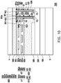
- FIG. 10 is a sectional schematic view of a manufacturing process of a display apparatus of a tenth embodiment of the disclosure.
- connection may mean physical and/or electrical connection.
- electrically connected to or “coupled to” may mean that another element exists between the two elements.
- “about”, “similarly”, “substantively” used in the present content includes the value and an average value within an acceptable deviation range of a specific value confirmed by persons skilled in the art. A specific number of errors related to a measurement (which is a limitation of a measurement system) as well as a discussed measurement are considered. For example, “about” may represent a range within one or a plurality of standard deviations of the value, or within ⁇ 30%, ⁇ 20%, ⁇ 10%, ⁇ 5%. Moreover, the “about”, “similar and “substantively” used in the present content may choose a more acceptable deviation range and standard deviation according to an optical nature, an etching nature or other natures rather than choosing one standard deviation to adapt all natures.
- FIG. 1A - FIG. 1E are sectional schematic views of a manufacturing process of a display apparatus of a first embodiment of the disclosure.
- the first circuit substrate includes a substrate 1 and a first circuit layer 100 disposed on the substrate 1 .
- the second circuit substrate includes a substrate 2 and a second circuit layer 200 disposed on the substrate 2 .
- the first circuit layer 100 may include a thin-film transistor T 1 .
- the thin-film transistor T 1 includes a semiconductor pattern 120 , an insulating sublayer 130 , a gate 141 , a first electrode 161 and a second electrode 162 .
- the insulating sublayer 130 is disposed between the gate 141 and the semiconductor pattern 120 .
- a first electrode 161 and a second electrode 162 are electrically connected to two different areas of the semiconductor pattern 120 respectively.
- the thin-film transistor T 1 may further optionally include an insulating sublayer 150 .
- the insulating sublayer 150 is disposed on the insulating sublayer 130 , and the first electrode 161 and the second electrode 162 may be disposed on the insulating sublayer 150 , but the disclosure is not limited herein.
- the first circuit layer 100 may further optionally include a buffering sublayer 110 and an insulating sublayer 170 .
- the buffering sublayer 110 is disposed on the substrate 1
- the thin-film transistor T 1 is disposed on the buffering sublayer 110
- the insulating sublayer 170 is disposed on the thin-film transistor T 1 , but the disclosure is not limited herein.
- the first circuit layer 100 may further optionally include a bus line 142 .
- the thin-film transistor T 1 of the first circuit layer 100 is electrically connected to the bus line 142 of the first circuit layer 100 .
- the bus line 142 may form in a same film layer with the gate 141 .
- the disclosure is not limited herein.
- the bus line 142 may form in a same film layer with the first electrode 161 and/or the second electrode 162 .
- the second circuit layer 200 may include a thin-film transistor T 2 .
- the thin-film transistor T 2 includes a semiconductor pattern 220 , an insulating sublayer 230 , a gate 241 , a first electrode 261 and a second electrode 262 .
- the insulating sublayer 230 is disposed between the gate 241 and the semiconductor pattern 220 .
- the first electrode 261 and the second electrode 262 are electrically connected to two different areas of the semiconductor 220 respectively.
- the thin-film transistor T 2 may further optionally include an insulating sublayer 250 .
- the insulating sublayer 250 is disposed on the insulating sublayer 230 , and the first electrode 261 and the second electrode 262 may be disposed on the insulating sublayer 250 , but the disclosure is not limited herein.
- the second circuit layer 200 may further optionally include a buffering sublayer 210 and an insulating sublayer 270 .
- the buffering sublayer 210 is disposed on the substrate 2
- the thin-film transistor T 2 is disposed on the buffering sublayer 210
- the insulating sublayer 270 is disposed on the thin-film transistor T 2 , but the disclosure is not limited herein.
- the second circuit layer 200 may further optionally include a bus line 242 .
- the thin-film transistor T 2 of the second circuit layer 200 is electrically connected to the bus line 242 of the second circuit layer 200 .
- the bus line 242 may form in a same film layer with the gate 241 .
- the disclosure is not limited herein. According to other embodiments, the bus line 242 may form in a same film layer with the first electrode 261 and/or the second electrode 262 .
- the first electrodes 161 and 261 , the second electrodes 162 and 262 , the gates 141 and 241 and the bus lines 142 and 242 of the first circuit layer 100 and the second circuit layer 200 generally use metal materials, but the disclosure is not limited herein. According to other embodiments, the first electrodes 161 and 261 , the second electrodes 162 and 262 , the gates 141 and 241 and the bus lines 142 and 242 of the first circuit layer 100 and the second circuit layer 200 may use other conductive materials such as alloy, nitrides of metal materials, oxides of metal materials, oxynitrides of metal materials, or stack layers of metal materials with other conductive materials.
- the buffering sublayers 110 and 210 and the insulating sublayers 130 , 150 , 170 , 230 , 250 and 270 of the first circuit layer 100 and the second circuit layer 200 may be inorganic materials (such as silicon dioxide, silicon nitride, silicon oxynitride, or a stack layer of the at least two materials), organic materials or combinations thereof.
- a bonding process is performed, which means using a first adhesive layer 300 to connect the first circuit substrate and the second circuit substrate.
- the first adhesive layer 300 is disposed on the first circuit layer 100
- the second circuit layer 200 is disposed on the first adhesive layer 300 .
- the first adhesive layer 300 is an insulating adhesive layer.
- the insulating sublayer 170 of the first circuit layer 100 has a surface 170 k facing away from the semiconductor pattern 120 .
- the insulating sublayer 270 of the second circuit payer 200 has a surface 270 k facing away from the semiconductor pattern 220 .
- the surface 170 k of the first circuit layer 100 facing away from the semiconductor pattern 120 may optionally face upward, and the surface 270 k of the second circuit layer 200 facing away from the semiconductor pattern 220 may optionally face downward, but the disclosure is not limited herein.
- the substrate 2 of the second circuit substrate is removed, and the second circuit layer 200 of the second circuit substrate is left on the first adhesive layer 300 .
- vias 210 a , 210 b , 210 c , 210 d and 210 e of the buffering sublayer 210 vias 230 a , 230 b , 230 c , 230 d , and 230 e of the insulating sublayer 230 , vias 250 a , 250 b , 250 c , and 250 d of the insulating sublayer 250 , vias 270 a and 270 d of the insulating sublayer 270 , vias 300 a and 300 d of the first adhesive layer 300 , vias 170 a and 170 d of the insulating sublayer 170 , and a via 150 d of the insulating sublayer 150 .
- the patterning process may include production processes such as photoresist coating, photoresist exposure and development, etching and photoresist removal.
- a same patterning photoresist may be used as a cover, etching the buffering sublayer 210 , the insulating sublayer 230 , the insulating sublayer 250 , the insulating sublayer 270 , the first adhesive layer 300 , the insulating sublayer 170 and the insulating sublayer 150 .
- the via 210 a of the buffering sublayer 210 , the via 230 a of the insulating sublayer 230 , the via 250 a of the insulating sublayer 250 , the via 270 a of the insulating sublayer 270 , the via 300 a of the first adhesive layer 300 , and the via 170 a of the insulating sublayer 170 may be aligned substantively.
- the via 210 d of the buffering sublayer 210 , the via 230 d of the insulating sublayer 230 , the via 250 d of the insulating sublayer 250 , the via 270 d of the insulating sublayer 270 , the via 300 d of the first adhesive layer 300 , the via 170 d of the insulating sublayer 170 and the via 150 d of the insulating sublayer 150 may be substantively aligned.
- the via 210 a of the buffering sublayer 210 , the via 230 a of the insulating sublayer 230 , the via 250 a of the insulating sublayer 250 , the via 270 a of the insulating sublayer 270 , the via 300 a of the first adhesive layer 300 , the via 170 a of the insulating sublayer 170 and a part of the thin-film transistor T 1 may define a groove U 1 .
- the groove U 1 is located outside of the semiconductor pattern 220 of the thin-film transistor T 2 . In other words, the groove U 1 does not overlap the semiconductor pattern 220 of the thin-film transistor T 2 .
- the via 210 b of the buffering sublayer 210 , the via 230 b of the insulating sublayer 230 , the via 250 b of the insulating sublayer 250 and a part of the thin-film transistor T 2 may define a groove U 2 .
- the groove U 2 is located outside of the semiconductor pattern 220 of the thin-film transistor T 2 . In other words, the groove U 2 does not overlap the semiconductor pattern 220 of the thin-film transistor T 2 .
- the via 210 c of the buffering sublayer 210 , the via 230 c of the insulating sublayer 230 , the via 250 c of the insulating sublayer 250 and a part of the thin-film transistor T 2 may define a groove U 3 .
- the groove U 3 is located outside of the semiconductor pattern 220 of the thin-film transistor T 2 . In other words, the groove U 3 does not overlap the semiconductor pattern 220 of the thin-film transistor T 2 .
- the via 210 d of the buffering sublayer 210 , the via 230 d of the insulating sublayer 230 , the via 250 d of the insulating sublayer 250 , the via 270 d of the insulating sublayer 270 , the via 300 d of the first adhesive layer 300 , the via 170 d of the insulating sublayer 170 , the via 150 d of the insulating sublayer 150 , and the bus line 142 may define a groove U 4 .
- the groove U 4 is located outside of the semiconductor pattern 220 of the thin-film transistor T 2 and the semiconductor pattern 120 of the thin-film transistor T 1 . In other words, the groove U 4 does not overlap the semiconductor pattern 220 of the thin-film transistor T 2 and the semiconductor pattern 120 of the thin-film transistor T 1 .
- the via 210 e of the buffering sublayer 210 , the via 230 e of the insulating sublayer 230 and the bus line 242 may define a groove U 5 .
- the groove U 5 is located outside of the semiconductor pattern 220 of the thin-film transistor T 2 . In other words, the groove U 5 does not overlap the semiconductor pattern 220 of the thin-film transistor T 2 .
- a first conductive element 411 , a second conductive element 412 and a pixel electrode 510 are formed on the second circuit layer 200 .
- the first conductive element 411 is disposed on the second circuit layer 200 , and is electrically connected to the first circuit layer 100 and the second circuit layer 200 .
- the first conductive element 411 may be electrically connected to the thin-film transistor T 1 of the first circuit layer 100 and the thin-film transistor T 2 of the second circuit layer 200 through the vias 210 a and 210 b of the buffering sublayer 210 , the vias 230 a and 230 b of the insulating sublayer 230 , the vias 250 a and 250 b of the insulating sublayer 250 , the via 270 a of the insulating sublayer 270 , the via 300 a of the first adhesive layer 300 and the via 170 a of the insulating sublayer 170 .
- the second conductive element 412 is disposed on the second circuit layer 200 .
- the second conductive element 412 is electrically connected to the bus line 142 of the first circuit layer 100 and the bus line 242 of the second circuit layer 200 through the vias 210 d and 210 e of the buffering sublayer 210 , the vias 230 d and 230 e of the insulating sublayer 230 , the via 250 d of the insulating sublayer 250 , the via 270 d of the insulating sublayer 270 , the via 300 d of the first adhesive layer 300 , the via 170 d of the insulating sublayer 170 , and the via 150 d of the insulating sublayer 150 .
- the pixel electrode 510 is disposed on the second circuit layer 200 , and is electrically connected to the second circuit layer 200 .
- the pixel electrode 510 is electrically connected to the thin-film transistor T 2 of the second circuit layer 200 through the via 210 c of the buffering sublayer 210 , the via 230 c of the insulating sublayer 230 , the via 250 c of the insulating sublayer 250 .
- a sputtering production process may be used to form the first conductive element 411 , the second conductive element 412 and the pixel electrode 250 .
- a part of the first conductive element 411 may be conformally disposed in the groove U 1 defined by the via 210 a of the buffering sublayer 210 , the via 230 a of the insulating sublayer 230 , the via 250 a of the insulating sublayer 250 , the via 270 a of the insulating sublayer 270 , the via 300 a of the first adhesive layer 300 , the via 170 a of the insulating sublayer 170 and a part of the thin-film transistor T 1 (for example but not limited to: the first electrode 161 ).
- Another part of the first conductive element 411 may be conformally disposed in the groove U 2 defined by the via 210 b of the buffering sublayer 210 , the via 230 b of the insulating sublayer 230 , the via 250 b of the insulating sublayer 250 and a part of the thin-film-transistor T 2 (for example but not limited to: the first electrode 261 ).
- a part of the second conductive element 412 may be conformally disposed in the groove U 4 defined by the via 210 d of the buffering sublayer 210 , the via 230 d of the insulating sublayer 230 , the via 250 d of the insulating sublayer 250 , the via 270 d of the insulating sublayer 270 , the via 300 d of the first adhesive layer 300 , the via 170 d of the insulating sublayer 170 , the via 150 d of the insulating sublayer 150 and the bus line 142 .
- Another part of the second conductive element 412 may be conformally disposed in the groove U 5 defined by the via 210 e of the buffering sublayer 210 , the via 230 e of the insulating sublayer 230 and the bus line 242 .
- a part of the pixel electrode 510 may be conformally disposed in the groove U 3 defined by the via 210 c of the buffering sublayer 210 , the via 230 c of the insulating sublayer 230 , the via 250 c of the insulating sublayer 250 and a part of the thin-film transistor T 2 (for example: the second electrode 262 ).
- a pixel defining sublayer 520 is formed on the pixel electrode 510 and the second circuit layer 200 .
- the pixel defining sublayer 520 is disposed on the pixel electrode 510 , and has a via 520 a overlapping the pixel electrode 510 .
- an organic electroluminescent material 530 is formed, and is disposed in the via 520 a of the pixel defining sublayer 520 .
- a common electrode 540 is formed, and is disposed on the organic electroluminescent material 530 .
- a display element layer 500 includes the pixel electrode 510 , the pixel defining sublayer 520 , the organic electroluminescent material 530 and the common electrode 540 .
- a part of the first conductive element 411 used to electrically connect the first circuit layer 100 and the second circuit layer 200 is disposed between the pixel defining sublayer 520 and the second circuit layer 200 (for example: the insulating sublayer 230 of the second circuit layer 200 ).
- a part of the second conductive element 412 used to electrically connect the first circuit layer 100 and the second circuit layer 200 is disposed between the pixel defining sublayer 520 and the second circuit layer 200 (for example: the second circuit layer 200 and the insulating sublayer 230 ).
- the first conductive element 411 and the second conductive element 412 used to electrically connect the first circuit layer 100 and the second circuit layer 200 are formed on the second circuit layer 200 , inside the second circuit layer 200 and inside the first circuit layer 100 after the first circuit layer 100 and the second circuit layer 200 are bonded. Therefore, even though the bonding precision of the first circuit layer 100 and the second circuit layer 200 is not high, the first circuit layer 100 and the second circuit layer 200 may still be electrically connected to each other using the first conductive element 411 and the second conductive element 412 formed after the bonding process, so as to greatly decrease the manufacturing difficulty of the display apparatus 10 .
- FIG. 2 is a sectional schematic view of a display apparatus of a second embodiment of the disclosure.
- a display apparatus 10 A of FIG. 2 is similar to the display apparatus 10 of FIG. 1E .
- the difference of the two apparatuses lies in that the surface 170 k of the first circuit layer 100 of the display apparatus 10 A and the surface 270 k of the second circuit layer 200 of the display apparatus 10 A both face upward.
- FIG. 3 is a sectional schematic view of a display apparatus of a third embodiment of the disclosure.
- a display apparatus 10 B of FIG. 3 is similar to the display apparatus 10 of FIG. 1E .
- the difference of the two apparatuses lies in that the surface 170 k of the insulating sublayer 170 of the first circuit layer 100 of the display apparatus 10 B and the surface 270 k of the insulating sublayer 270 of the second circuit layer 200 of the display apparatus 10 B both face downward.
- FIG. 4 is a sectional schematic view of a display apparatus of a fourth embodiment of the disclosure.
- a display apparatus 10 C of FIG. 4 is similar to the display 10 of FIG. 1E .
- the difference of the two apparatuses lies in that the surface 170 k of the first circuit layer 100 of the display apparatus 10 C faces downward and the surface 270 k of the second circuit layer 200 of the display apparatus 10 C faces upward.
- FIG. 5 is a sectional schematic view of a display apparatus of a fifth embodiment of the disclosure.
- a display apparatus 10 D of FIG. 5 is similar to the display 10 C of FIG. 4 .
- the difference of the two apparatuses lies as follows. Please refer to FIG. 5 .
- a first electrode 261 C and a second electrode 262 C of the thin-film transistor T 2 form in a same film layer with at least one part of the first conductive element 411 .
- the first electrode 261 C and the second electrode 262 C of the thin-film transistor T 2 and the first conductive element 411 may be manufactured together. Therefore, compared to the display apparatus 10 C of FIG. 4 , the display apparatus 10 D of FIG. 5 further has advantages of simplifying manufacturing process and reducing manufacturing costs.
- FIG. 6 is a sectional schematic view of a display apparatus of a sixth embodiment of the disclosure.
- a display apparatus 10 E of FIG. 6 is similar to the display apparatus 10 D of FIG. 1E .
- the difference of the two apparatuses lies as follows.
- the first adhesive layer 300 may be formed in advance on the first circuit layer 100 ; then, before the second circuit layer 200 bonds with the first circuit layer 100 , the vias 300 a and 300 d of the first adhesive layer 300 , the vias 170 a and 170 d of the insulating sublayer 170 of the first circuit layer 100 , and the via 150 d of the insulating sublayer 150 of the first circuit layer 100 are formed, and a first portion 411 a is formed in advance in the vias 170 a and 300 a , forming a first portion 412 a in the vias 300 d , 170 d and 150 d ; further, the second circuit layer 200 and the first circuit layer 100 are then bonded; further, the vias 210 a and 210 d of the insulating sublayer 210 , the vias 230 a and 230 d of the insulating sublayer 230 , the vias 250 a and 250
- the first portion 411 a and the second portion 411 b of the first conductive element 411 are formed in different manufacturing process, the first portion 411 a and the second portion 411 b of the first conductive element 411 has an interface S 1 .
- the first portion 412 a and the second portion 412 b of the second conductive element 412 are formed in different manufacturing processes, the first portion 412 a and the second portion 412 b of the second conductive element 412 has an interface S 2 .
- the display element layer 500 is driven by a driving circuit, and the driving circuit may be composed of a plurality of circuit layers (such as the first circuit layer 100 and the second circuit layer 200 ) separated by at least one adhesive layer (such as the first adhesive layer 300 ).
- the driving circuit used to drive the display element layer 500 may be a structure of 7 thin-film transistors and one capacitor (7T1C), and the thin-film transistor T 1 of the first circuit layer and the thin-film transistor T 2 of the second circuit layer 200 may be two thin-film transistors of the first electrodes 161 and 261 of the 7T1C driving circuit electrically connected to each other.
- 7T1C 7 thin-film transistors and one capacitor
- the driving circuit used to drive the display element layer 500 may be other structures, and/or the thin-film transistor T 1 of the first circuit layer 100 and the thin-film transistor T 2 of the second circuit layer 200 may be electrically connected by other methods. Examples are raised with FIG. 7 in the following content.
- FIG. 7 is a sectional schematic view of a display apparatus of a seventh embodiment of the disclosure.
- the display apparatus 10 F of FIG. 7 is similar to the display apparatus 10 of FIG. 1E , and the difference of the two apparatuses lies as follows.
- a driving circuit used to drive the display element layer 520 may be a structure of 2 thin-film transistors and one capacitor (2T1C).
- the thin-film transistor T 1 of the first circuit layer 100 and the thin-film transistor T 2 of the second circuit layer 200 may be respectively a switching TFT and a driving TFT of the 2T1C driving circuit, and the first electrode 161 of the thin-film transistor T 1 of the first circuit layer 100 and the gate 241 of the thin-film transistor T 2 of the second circuit layer 200 use the first conductive element 411 to be electrically connected to each other.
- the display apparatus 10 F further includes a second adhesive layer 600 , a third element layer 700 and a third conductive element 413 .
- the second adhesive layer 600 is disposed between the first circuit layer 100 and the substrate 1 .
- the third element layer 700 includes a bus line 710 .
- the bus line 710 is disposed between the second adhesive layer 600 and the substrate 1 .
- the third conductive element 412 is disposed on the first circuit layer 100 , and is electrically connected to the thin-film transistor T 1 of the first circuit layer 100 , wherein the third conductive element 413 is electrically connected to the bus line 710 of the third element layer 700 through a via 600 f of the second adhesive layer 600 .
- the insulating sublayer 170 has a via 170 f disposed outside of the semiconductor pattern 120
- the insulating sublayer 150 has a via 150 f disposed outside of the semiconductor pattern 120
- the insulating sublayer 130 has a via 130 f disposed outside of the semiconductor pattern 120
- the buffering sublayer 110 has a via 110 f disposed outside of the semiconductor pattern 120
- the third conductive element 413 may be electrically connected to the bus line 710 of the third element layer 700 through the via 170 f of the insulating sublayer 170 , the via 150 f of the insulating sublayer 150 , the via 130 f of the insulating sublayer 130 , the via 110 f of the buffering sublayer 110 and the via 600 f of the second adhesive layer 600 .
- the via 170 f of the insulating sublayer 170 , the via 150 f of the insulating sublayer 150 , the via 130 f of the insulating sublayer 130 , the via 110 f of the buffering sublayer 110 and the via 600 f of the second adhesive layer 600 are substantively aligned, but the disclosure is not limited herein.
- a groove U 6 may be defined by the via 170 f of the insulating sublayer 170 , the via 150 f of the insulating sublayer 150 , the via 130 f of the insulating sublayer 130 , the via 110 f of the buffering sublayer 110 , the via 600 f of the second adhesive layer 600 and the bus line 710 .
- the groove U 6 is disposed outside of the semiconductor pattern 120 of the first circuit layer 100 , and a part of the third conductive element 412 may be conformally disposed in the groove U 6 .
- FIG. 8A - FIG. 8D are sectional schematic views of a manufacturing process of a display apparatus of an eighth embodiment of the disclosure.
- the display substrate on a lower part of FIG. 8A includes the substrate 1 , the first circuit layer 100 , the second circuit layer 200 and the display element layer 500 .
- the first circuit layer 100 , the second circuit layer 200 and the display element layer 500 are schematically shown in FIG. 8 A, and detailed structures are omitted.
- the touch substrate on an upper part of FIG. 8A includes a substrate 3 and a touch element layer 800 disposed on the substrate 3 .
- the display substrate on a lower part of FIG. 8A further includes pads P 1 and P 2 disposed on the substrate 1 .
- the pads P 1 and P 2 are used for an assembling of a driving chip, so as to allowed the touch element layer 800 on an upper part of FIG. 8A to be driven by the driving chip.
- the pads P 1 and P 2 are shown to be disposed on the second circuit layer 200 as an example; however, the disclosure is not limited herein. According to other embodiments, the pads P 1 and P 2 may also be disposed to the first circuit layer 100 , to the second circuit layer 200 or inside a combination thereof.
- the touch element layer 800 may include a buffering sublayer 810 , a sensing electrode 821 a and peripheral wirings 821 b and 841 b disposed on the buffering sublayer 810 , an insulating sublayer 830 disposed on the sensing electrode 821 a and the peripheral wirings 821 b and 841 b , a sensing electrode 841 a disposed on the insulating sublayer 830 and an insulating sublayer 850 disposed on the sensing electrode 841 a .
- the sensing electrode 821 a is electrically connected to the peripheral wiring 821 b .
- the sensing electrode 841 a may be electrically connected to the peripheral wiring 841 b through a via 833 of the insulating sublayer 830 .
- a bonding process is performed, which means a first adhesive layer 930 is used to connect the touch substrate and the display substrate.
- the first adhesive layer 930 is disposed on the display element layer 500 and the pads P 1 and P 2
- the touch element layer 800 is disposed on the first adhesive layer 930 .
- the insulating sublayers 830 and 850 are disposed between the sensing electrode 821 a and the first adhesive layer 930 and between the peripheral wirings 841 b and 821 b and the first adhesive layer 930 .
- FIG. 8A and FIG. 8B Please refer to FIG. 8A and FIG. 8B .
- the substrate 3 of the touch substrate is removed, and the touch element layer 800 is left on the first adhesive layer 930 .
- the vias 811 a , 811 b , 812 a and 812 b of the buffering sublayer 810 , the vias 831 and 832 of the insulating sublayer 830 , the vias 851 and 852 of the insulating sublayer 850 and the vias 931 and 932 of the first adhesive layer 930 are formed through using the patterning process for at least one time.
- the patterning process may include production processes such as photoresist coating, photoresist exposing and development, etching and photoresist removal.
- a same patterning photoresist may be used as a cover, etching the buffering sublayer 810 , the insulating sublayer 830 , the insulating sublayer 850 and the first adhesive layer 930 .
- the via 811 a of the insulating sublayer 810 , the via 831 of the insulating sublayer 830 , the via 851 of the insulating sublayer 850 and the via 931 of the first adhesive sublayer 930 are substantively aligned.
- a groove U 1 ′ may be defined by the via 811 a of the buffering sublayer 810 , the via 831 of the insulating sublayer 830 , the via 851 of the insulating sublayer 850 , the via 931 of the first adhesive layer 930 and the pad P 1 .
- the via 812 a of the buffering sublayer 810 , the via 832 of the insulating sublayer 830 , the via 852 of the insulating sublayer 850 , and the via 932 of the first adhesive layer 930 may be substantively aligned.
- a groove U 2 ′ may be defined by the via 812 a of the buffering sublayer 810 , the via 832 of the insulating sublayer 830 , the via 852 of the insulating sublayer 850 , the via 932 of the first adhesive layer 930 and the pad P 2 .
- a conductive element 910 and a conductive element 920 are formed on the touch element layer 800 .
- the conductive elements 910 and 920 are disposed on the touch element layer 800 , and are electrically connected to the touch element layer 800 .
- the conductive element 910 may be electrically connected to the peripheral wiring 821 b through the via 811 b of the buffering sublayer 810
- the conductive element 920 may be electrically connected to the peripheral wiring 841 b through the via 812 b of the buffering sublayer 810 .
- the conductive elements 910 and 920 are electrically connected to the pads P 1 and P 2 through the vias 931 and 932 of the first adhesive layer 930 .
- the conductive elements 910 and 920 may be electrically connected to the pad P 1 through the via 811 a of the buffering sublayer 810 , the via 831 of the insulating sublayer 830 , the via 851 of the insulating sublayer 850 and the via 931 of the first adhesive layer 930
- the conductive element 920 may be electrically connected to the pad P 2 through the via 812 a of the buffering sublayer 810 , the via 832 of the insulating sublayer 830 , the via 852 of the insulating sublayer 850 and the via 932 of the first adhesive layer 930 .
- a sputtering production process may be used to form the conductive elements 910 and 920 . Therefore, a part of the conductive element 910 may be conformally disposed in a groove U 1 ′ defined by the via 811 a of the buffering sublayer 810 , the via 831 of the insulating sublayer 830 , the via 851 of the insulating sublayer 850 , the via 931 of the first adhesive layer 930 and the pad P 1 , and a part of the conductive element 920 may be conformally disposed in a groove U 2 ′ defined by the via 812 a of the buffering sublayer 810 , the via 832 of the insulating sublayer 830 , the via 852 of the insulating sublayer 850 , the via 932 of the first adhesive layer 930 and the pad P 2 .
- a bonding process is performed, which means that a second adhesive layer 940 is used to connect a covering plate 4 and the touch element layer 800 .
- the second adhesive layer 940 is disposed on the touch element layer 800 , and a part of each of the conductive elements 910 and 920 is disposed between the second adhesive layer 940 and the touch element layer 800 .
- the covering plate 4 is disposed on the second adhesive layer 940 .
- the sensing electrode 821 a and the peripheral wiring 821 b are disposed between the insulating sublayer 830 and the buffering sublayer 810
- the insulating sublayer 830 is disposed between the sensing electrode 821 a and the first adhesive layer 930 and between the peripheral wiring 821 b and the first adhesive layer 930
- the buffering sublayer 810 is disposed between the sensing electrode 821 a and the second adhesive layer 940 and between the peripheral wiring 821 b and the second adhesive layer 940
- the conductive element 910 is disposed on the buffering sublayer 810 and is electrically connected to the peripheral wiring 821 b through the via 811 b of the buffering sublayer 810 .
- the sensing electrode 841 a and the peripheral wiring 841 b are disposed between the insulating sublayer 850 and the buffering sublayer 810
- the insulating sublayer 850 is disposed between the sensing electrode 841 a and the first adhesive layer 930 and between the peripheral wiring 841 b and the first adhesive layer 930
- the buffering sublayer 810 is disposed between the sensing electrode 841 a and the second adhesive layer 940 and between the peripheral wiring 841 b and the second adhesive layer 940
- the conductive element 920 is disposed on the buffering sublayer 810 and is electrically connected to the peripheral wiring 841 b through the via 812 b of the buffering sublayer 810 .
- the conductive elements 910 and 920 used to electrically connect the touch element layer 800 and the pads P 1 and P 2 are formed on the touch element layer 800 , inside the touch element layer 800 and inside the first adhesive layer 930 after the bonding of the touch element layer 800 with the circuit layers 100 and 200 and the display element layer 500 .
- the conductive elements 910 and 920 may electrically connect the touch element layer 800 and the pads P 1 and P 2 finely, and the bending tolerance of the conductive elements 910 and 920 is good.
- FIG. 9 is a sectional schematic view of a manufacturing process of a display apparatus of a ninth embodiment of the disclosure.
- a display apparatus 20 A of FIG. 9 is similar to the display apparatus 20 of FIG. 8D .
- the difference of the two display apparatuses lies in that the display apparatus 20 A of FIG. 9 may not include the buffering sublayer 810 of FIG. 8D , a part of the conductive element 910 of FIG. 9 may directly cover on the peripheral wiring 821 b , and a part of the conductive element 920 of FIG. 9 may directly cover on the peripheral wiring 841 b.
- FIG. 10 is a sectional schematic view of a manufacturing process of a display apparatus of a tenth embodiment of the disclosure.
- a display apparatus 20 B of FIG. 10 is similar to the display apparatus 20 of FIG. 8D .
- the difference of the two display apparatuses lies as follows.
- the first adhesive layer 930 may be formed on the display element layer 500 and the pads P 1 and P 2 ; then, before the bonding of the touch element layer 800 with the display element layer 500 and the pads P 1 and P 2 , vias 931 and 932 of the first adhesive layer 930 are formed, and first portions 911 and 921 are formed in the vias 931 and 932 in advance; further, the touch element layer 800 is bonded with the display element layer 500 and the pads P 1 and P 2 ; then, the vias 811 a and 811 b of the buffering sublayer 810 , the vias 831 and 832 of the insulating sublayer 830 and the vias 851 and 852 of the insulating sublayer 850 are formed; further, a second portion 912 is formed in the vias 811 a , 831 and 851 , and a second portion 922 is formed in the vias 812 a , 832 and 852 , wherein the
- the first portion 911 and the second portion 912 of the conductive element 910 are formed in different manufacturing processes, the first portion 911 and the second portion 912 of the conductive element 910 has an interface S 1 .
- the first portion 921 and the second portion 922 of the conductive element 920 are formed in different manufacturing processes, the first portion 921 and the second portion 922 of the second conductive element 920 has an interface S 2 .
Landscapes
- Engineering & Computer Science (AREA)
- General Engineering & Computer Science (AREA)
- Theoretical Computer Science (AREA)
- Microelectronics & Electronic Packaging (AREA)
- Physics & Mathematics (AREA)
- Human Computer Interaction (AREA)
- General Physics & Mathematics (AREA)
- Geometry (AREA)
- Computer Networks & Wireless Communication (AREA)
- Devices For Indicating Variable Information By Combining Individual Elements (AREA)
- Electroluminescent Light Sources (AREA)
Abstract
Description
Claims (12)
Applications Claiming Priority (2)
| Application Number | Priority Date | Filing Date | Title |
|---|---|---|---|
| TW108111003 | 2019-03-28 | ||
| TW108111003A TWI710820B (en) | 2019-03-28 | 2019-03-28 | Display apparatus |
Publications (2)
| Publication Number | Publication Date |
|---|---|
| US20200312829A1 US20200312829A1 (en) | 2020-10-01 |
| US11088129B2 true US11088129B2 (en) | 2021-08-10 |
Family
ID=69200631
Family Applications (1)
| Application Number | Title | Priority Date | Filing Date |
|---|---|---|---|
| US16/502,046 Active 2039-07-04 US11088129B2 (en) | 2019-03-28 | 2019-07-03 | Display apparatus |
Country Status (3)
| Country | Link |
|---|---|
| US (1) | US11088129B2 (en) |
| CN (1) | CN110707102B (en) |
| TW (1) | TWI710820B (en) |
Families Citing this family (2)
| Publication number | Priority date | Publication date | Assignee | Title |
|---|---|---|---|---|
| CN113410176B (en) * | 2020-03-16 | 2023-10-27 | 合肥晶合集成电路股份有限公司 | OLED devices and manufacturing methods |
| KR102951802B1 (en) * | 2020-07-30 | 2026-04-14 | 삼성디스플레이 주식회사 | Display device and method of fabricating the same |
Citations (8)
| Publication number | Priority date | Publication date | Assignee | Title |
|---|---|---|---|---|
| US20150044792A1 (en) | 2013-08-06 | 2015-02-12 | Semiconductor Energy Laboratory Co., Ltd. | Peeling Method |
| CN104752484A (en) | 2013-12-26 | 2015-07-01 | 乐金显示有限公司 | Organic Light Emitting Diode Display Device With Touch Screen And Method Of Fabricating The Same |
| US20150214286A1 (en) * | 2014-01-27 | 2015-07-30 | Boe Technology Group Co., Ltd. | Array substrate, method for manufacturing the same, display device and electronic product |
| US20150270307A1 (en) | 2012-10-18 | 2015-09-24 | Sony Corporation | Semiconductor device, solid-state imaging device and electronic apparatus |
| US20150311260A1 (en) | 2014-04-25 | 2015-10-29 | Semiconductor Energy Laboratory Co., Ltd. | Input and output device |
| US20150309377A1 (en) * | 2013-05-30 | 2015-10-29 | Boe Technology Group Co., Ltd. | Array substrate, manufacturing method, and display device thereof |
| CN105845708A (en) | 2016-04-20 | 2016-08-10 | 上海天马微电子有限公司 | Flexible integrated touch display panel and manufacturing method thereof |
| CN106601772A (en) | 2016-12-13 | 2017-04-26 | 上海天马有机发光显示技术有限公司 | Organic light-emitting display panel, organic light-emitting display device and preparation method |
Family Cites Families (5)
| Publication number | Priority date | Publication date | Assignee | Title |
|---|---|---|---|---|
| WO2006098390A1 (en) * | 2005-03-15 | 2006-09-21 | Semiconductor Energy Laboratory Co., Ltd. | Semiconductor device and electronic device having the same |
| US8049253B2 (en) * | 2007-07-11 | 2011-11-01 | Semiconductor Energy Laboratory Co., Ltd. | Semiconductor device and method for manufacturing the same |
| US9356049B2 (en) * | 2013-07-26 | 2016-05-31 | Semiconductor Energy Laboratory Co., Ltd. | Display device with a transistor on an outer side of a bent portion |
| JP2015228367A (en) * | 2014-05-02 | 2015-12-17 | 株式会社半導体エネルギー研究所 | Semiconductor device, input / output device, and electronic device |
| JP6263093B2 (en) * | 2014-06-25 | 2018-01-17 | ルネサスエレクトロニクス株式会社 | Semiconductor device |
-
2019
- 2019-03-28 TW TW108111003A patent/TWI710820B/en active
- 2019-07-03 US US16/502,046 patent/US11088129B2/en active Active
- 2019-10-18 CN CN201910993393.3A patent/CN110707102B/en active Active
Patent Citations (19)
| Publication number | Priority date | Publication date | Assignee | Title |
|---|---|---|---|---|
| US20180350867A1 (en) | 2012-10-18 | 2018-12-06 | Sony Corporation | Semiconductor device, solid-state imaging device and electronic apparatus |
| US20170148839A1 (en) | 2012-10-18 | 2017-05-25 | Sony Corporation | Semiconductor device, solid-state imaging device and electronic apparatus |
| US20180122850A1 (en) | 2012-10-18 | 2018-05-03 | Sony Corporation | Semiconductor device, solid-state imaging device and electronic apparatus |
| US9917131B2 (en) | 2012-10-18 | 2018-03-13 | Sony Corporation | Semiconductor device, solid-state imaging device and electronic apparatus |
| US20150270307A1 (en) | 2012-10-18 | 2015-09-24 | Sony Corporation | Semiconductor device, solid-state imaging device and electronic apparatus |
| CN107425021A (en) | 2012-10-18 | 2017-12-01 | 索尼公司 | Semiconductor device, solid camera head and electronic equipment |
| US10128301B2 (en) | 2012-10-18 | 2018-11-13 | Sony Corporation | Semiconductor device, solid-state imaging device and electronic apparatus |
| US20160218135A1 (en) | 2012-10-18 | 2016-07-28 | Sony Corporation | Semiconductor device, solid-state imaging device and electronic apparatus |
| US9570499B2 (en) | 2012-10-18 | 2017-02-14 | Sony Corporation | Semiconductor device, solid-state imaging device and electronic apparatus |
| US9431450B2 (en) | 2012-10-18 | 2016-08-30 | Sony Corporation | Semiconductor device, solid-state imaging device and electronic apparatus |
| US20150309377A1 (en) * | 2013-05-30 | 2015-10-29 | Boe Technology Group Co., Ltd. | Array substrate, manufacturing method, and display device thereof |
| US20150044792A1 (en) | 2013-08-06 | 2015-02-12 | Semiconductor Energy Laboratory Co., Ltd. | Peeling Method |
| CN104752484A (en) | 2013-12-26 | 2015-07-01 | 乐金显示有限公司 | Organic Light Emitting Diode Display Device With Touch Screen And Method Of Fabricating The Same |
| US9501165B2 (en) | 2013-12-26 | 2016-11-22 | Lg Display Co., Ltd. | Organic light emitting diode display device with touch screen and method of fabricating the same |
| US20150185942A1 (en) | 2013-12-26 | 2015-07-02 | Lg Display Co., Ltd. | Organic light emitting diode display device with touch screen and method of fabricating the same |
| US20150214286A1 (en) * | 2014-01-27 | 2015-07-30 | Boe Technology Group Co., Ltd. | Array substrate, method for manufacturing the same, display device and electronic product |
| US20150311260A1 (en) | 2014-04-25 | 2015-10-29 | Semiconductor Energy Laboratory Co., Ltd. | Input and output device |
| CN105845708A (en) | 2016-04-20 | 2016-08-10 | 上海天马微电子有限公司 | Flexible integrated touch display panel and manufacturing method thereof |
| CN106601772A (en) | 2016-12-13 | 2017-04-26 | 上海天马有机发光显示技术有限公司 | Organic light-emitting display panel, organic light-emitting display device and preparation method |
Non-Patent Citations (1)
| Title |
|---|
| Kazunori Watanabe et al., "An 8.67-in. Foldable OLED Display with an In-cell Touch Sensor," SID Symposium Digest of Technical Papers, vol. 46, Jul. 2015, pp. 246-249. |
Also Published As
| Publication number | Publication date |
|---|---|
| US20200312829A1 (en) | 2020-10-01 |
| CN110707102B (en) | 2022-03-29 |
| TWI710820B (en) | 2020-11-21 |
| TW202036106A (en) | 2020-10-01 |
| CN110707102A (en) | 2020-01-17 |
Similar Documents
| Publication | Publication Date | Title |
|---|---|---|
| US12201001B2 (en) | Array substrate and display device | |
| CN104617106B (en) | A kind of array base palte and display device | |
| US11251257B2 (en) | Manufacturing method of display panel having pad comprising embedded part and protruded part | |
| WO2022193699A1 (en) | Display substrate and display apparatus | |
| US11782547B2 (en) | Display substrate and manufacturing method therefor, and display device | |
| CN213182261U (en) | Display substrates, electronic devices | |
| WO2016141709A1 (en) | Array substrate and manufacturing method therefor, and display device | |
| CN121747427A (en) | Display devices | |
| CN112255849A (en) | Display substrate and electronic device | |
| WO2022236798A1 (en) | Display substrate, display panel, and display apparatus | |
| US11950463B2 (en) | Sub-power lines in non-display area and display device including the same | |
| WO2021190034A1 (en) | Display substrate and method for preparing same, and display apparatus | |
| CN101110430A (en) | Image display system having thin film transistor device and method of manufacturing the same | |
| CN107546242A (en) | Display device | |
| CN114823782B (en) | Display substrate, manufacturing method thereof and display device | |
| CN114551532A (en) | Display device and method of manufacturing the same | |
| US11088129B2 (en) | Display apparatus | |
| US20200321356A1 (en) | Array substrate and display device | |
| CN218831219U (en) | Display device | |
| CN114023257B (en) | Display panel, display panel driving method and display device | |
| US20250234712A1 (en) | Display device and method of providing the same | |
| WO2025175976A1 (en) | Array substrate, display panel and display module | |
| US20240122011A1 (en) | Display device | |
| US20240407217A1 (en) | Display substrate and display apparatus | |
| TWI710823B (en) | Display apparatus |
Legal Events
| Date | Code | Title | Description |
|---|---|---|---|
| AS | Assignment |
Owner name: AU OPTRONICS CORPORATION, TAIWAN Free format text: ASSIGNMENT OF ASSIGNORS INTEREST;ASSIGNOR:KE, TSUNG-YING;REEL/FRAME:049659/0565 Effective date: 20190612 |
|
| FEPP | Fee payment procedure |
Free format text: ENTITY STATUS SET TO UNDISCOUNTED (ORIGINAL EVENT CODE: BIG.); ENTITY STATUS OF PATENT OWNER: LARGE ENTITY |
|
| STPP | Information on status: patent application and granting procedure in general |
Free format text: FINAL REJECTION MAILED |
|
| STPP | Information on status: patent application and granting procedure in general |
Free format text: RESPONSE AFTER FINAL ACTION FORWARDED TO EXAMINER |
|
| STPP | Information on status: patent application and granting procedure in general |
Free format text: NOTICE OF ALLOWANCE MAILED -- APPLICATION RECEIVED IN OFFICE OF PUBLICATIONS |
|
| STPP | Information on status: patent application and granting procedure in general |
Free format text: PUBLICATIONS -- ISSUE FEE PAYMENT VERIFIED |
|
| STCF | Information on status: patent grant |
Free format text: PATENTED CASE |
|
| MAFP | Maintenance fee payment |
Free format text: PAYMENT OF MAINTENANCE FEE, 4TH YEAR, LARGE ENTITY (ORIGINAL EVENT CODE: M1551); ENTITY STATUS OF PATENT OWNER: LARGE ENTITY Year of fee payment: 4 |
|
| AS | Assignment |
Owner name: NEOLAYER LLC, TEXAS Free format text: ASSIGNMENT OF ASSIGNORS INTEREST;ASSIGNOR:AUO CORPORATION;REEL/FRAME:072266/0941 Effective date: 20250701 |