US11086349B2 - Reference voltage generator capable of reducing hot carrier stress - Google Patents
Reference voltage generator capable of reducing hot carrier stress Download PDFInfo
- Publication number
- US11086349B2 US11086349B2 US16/558,144 US201916558144A US11086349B2 US 11086349 B2 US11086349 B2 US 11086349B2 US 201916558144 A US201916558144 A US 201916558144A US 11086349 B2 US11086349 B2 US 11086349B2
- Authority
- US
- United States
- Prior art keywords
- voltage
- type transistor
- circuit
- output terminal
- terminal
- Prior art date
- Legal status (The legal status is an assumption and is not a legal conclusion. Google has not performed a legal analysis and makes no representation as to the accuracy of the status listed.)
- Active
Links
Images


Classifications
-
- G—PHYSICS
- G05—CONTROLLING; REGULATING
- G05F—SYSTEMS FOR REGULATING ELECTRIC OR MAGNETIC VARIABLES
- G05F3/00—Non-retroactive systems for regulating electric variables by using an uncontrolled element, or an uncontrolled combination of elements, such element or such combination having self-regulating properties
- G05F3/02—Regulating voltage or current
- G05F3/08—Regulating voltage or current wherein the variable is DC
- G05F3/10—Regulating voltage or current wherein the variable is DC using uncontrolled devices with non-linear characteristics
- G05F3/16—Regulating voltage or current wherein the variable is DC using uncontrolled devices with non-linear characteristics being semiconductor devices
- G05F3/20—Regulating voltage or current wherein the variable is DC using uncontrolled devices with non-linear characteristics being semiconductor devices using diode- transistor combinations
- G05F3/30—Regulators using the difference between the base-emitter voltages of two bipolar transistors operating at different current densities
-
- G—PHYSICS
- G05—CONTROLLING; REGULATING
- G05F—SYSTEMS FOR REGULATING ELECTRIC OR MAGNETIC VARIABLES
- G05F3/00—Non-retroactive systems for regulating electric variables by using an uncontrolled element, or an uncontrolled combination of elements, such element or such combination having self-regulating properties
- G05F3/02—Regulating voltage or current
- G05F3/08—Regulating voltage or current wherein the variable is DC
- G05F3/10—Regulating voltage or current wherein the variable is DC using uncontrolled devices with non-linear characteristics
- G05F3/16—Regulating voltage or current wherein the variable is DC using uncontrolled devices with non-linear characteristics being semiconductor devices
- G05F3/20—Regulating voltage or current wherein the variable is DC using uncontrolled devices with non-linear characteristics being semiconductor devices using diode- transistor combinations
- G05F3/22—Regulating voltage or current wherein the variable is DC using uncontrolled devices with non-linear characteristics being semiconductor devices using diode- transistor combinations wherein the transistors are of the bipolar type only
-
- G—PHYSICS
- G11—INFORMATION STORAGE
- G11C—STATIC STORES
- G11C11/00—Digital stores characterised by the use of particular electric or magnetic storage elements; Storage elements therefor
- G11C11/56—Digital stores characterised by the use of particular electric or magnetic storage elements; Storage elements therefor using storage elements with more than two stable states represented by steps, e.g. of voltage, current, phase, frequency
- G11C11/5621—Digital stores characterised by the use of particular electric or magnetic storage elements; Storage elements therefor using storage elements with more than two stable states represented by steps, e.g. of voltage, current, phase, frequency using charge storage in a floating gate
- G11C11/5642—Sensing or reading circuits; Data output circuits
-
- G—PHYSICS
- G11—INFORMATION STORAGE
- G11C—STATIC STORES
- G11C16/00—Erasable programmable read-only memories
- G11C16/02—Erasable programmable read-only memories electrically programmable
- G11C16/04—Erasable programmable read-only memories electrically programmable using variable threshold transistors, e.g. FAMOS
- G11C16/0408—Erasable programmable read-only memories electrically programmable using variable threshold transistors, e.g. FAMOS comprising cells containing floating gate transistors
- G11C16/0433—Erasable programmable read-only memories electrically programmable using variable threshold transistors, e.g. FAMOS comprising cells containing floating gate transistors comprising cells containing a single floating gate transistor and one or more separate select transistors
-
- G—PHYSICS
- G11—INFORMATION STORAGE
- G11C—STATIC STORES
- G11C16/00—Erasable programmable read-only memories
- G11C16/02—Erasable programmable read-only memories electrically programmable
- G11C16/06—Auxiliary circuits, e.g. for writing into memory
- G11C16/08—Address circuits; Decoders; Word-line control circuits
-
- G—PHYSICS
- G11—INFORMATION STORAGE
- G11C—STATIC STORES
- G11C16/00—Erasable programmable read-only memories
- G11C16/02—Erasable programmable read-only memories electrically programmable
- G11C16/06—Auxiliary circuits, e.g. for writing into memory
- G11C16/10—Programming or data input circuits
- G11C16/14—Circuits for erasing electrically, e.g. erase voltage switching circuits
-
- G—PHYSICS
- G11—INFORMATION STORAGE
- G11C—STATIC STORES
- G11C16/00—Erasable programmable read-only memories
- G11C16/02—Erasable programmable read-only memories electrically programmable
- G11C16/06—Auxiliary circuits, e.g. for writing into memory
- G11C16/24—Bit-line control circuits
-
- G—PHYSICS
- G11—INFORMATION STORAGE
- G11C—STATIC STORES
- G11C16/00—Erasable programmable read-only memories
- G11C16/02—Erasable programmable read-only memories electrically programmable
- G11C16/06—Auxiliary circuits, e.g. for writing into memory
- G11C16/26—Sensing or reading circuits; Data output circuits
- G11C16/28—Sensing or reading circuits; Data output circuits using differential sensing or reference cells, e.g. dummy cells
-
- G—PHYSICS
- G11—INFORMATION STORAGE
- G11C—STATIC STORES
- G11C16/00—Erasable programmable read-only memories
- G11C16/02—Erasable programmable read-only memories electrically programmable
- G11C16/06—Auxiliary circuits, e.g. for writing into memory
- G11C16/30—Power supply circuits
-
- G—PHYSICS
- G11—INFORMATION STORAGE
- G11C—STATIC STORES
- G11C16/00—Erasable programmable read-only memories
- G11C16/02—Erasable programmable read-only memories electrically programmable
- G11C16/06—Auxiliary circuits, e.g. for writing into memory
- G11C16/34—Determination of programming status, e.g. threshold voltage, overprogramming or underprogramming, retention
- G11C16/3404—Convergence or correction of memory cell threshold voltages; Repair or recovery of overerased or overprogrammed cells
-
- G—PHYSICS
- G11—INFORMATION STORAGE
- G11C—STATIC STORES
- G11C16/00—Erasable programmable read-only memories
- G11C16/02—Erasable programmable read-only memories electrically programmable
- G11C16/06—Auxiliary circuits, e.g. for writing into memory
- G11C16/34—Determination of programming status, e.g. threshold voltage, overprogramming or underprogramming, retention
- G11C16/3436—Arrangements for verifying correct programming or erasure
- G11C16/344—Arrangements for verifying correct erasure or for detecting overerased cells
- G11C16/3445—Circuits or methods to verify correct erasure of nonvolatile memory cells
-
- G—PHYSICS
- G11—INFORMATION STORAGE
- G11C—STATIC STORES
- G11C16/00—Erasable programmable read-only memories
- G11C16/02—Erasable programmable read-only memories electrically programmable
- G11C16/06—Auxiliary circuits, e.g. for writing into memory
- G11C16/34—Determination of programming status, e.g. threshold voltage, overprogramming or underprogramming, retention
- G11C16/3436—Arrangements for verifying correct programming or erasure
- G11C16/3454—Arrangements for verifying correct programming or for detecting overprogrammed cells
- G11C16/3459—Circuits or methods to verify correct programming of nonvolatile memory cells
-
- G—PHYSICS
- G11—INFORMATION STORAGE
- G11C—STATIC STORES
- G11C5/00—Details of stores covered by group G11C11/00
- G11C5/14—Power supply arrangements, e.g. power down, chip selection or deselection, layout of wirings or power grids, or multiple supply levels
- G11C5/147—Voltage reference generators, voltage or current regulators; Internally lowered supply levels; Compensation for voltage drops
-
- G—PHYSICS
- G11—INFORMATION STORAGE
- G11C—STATIC STORES
- G11C7/00—Arrangements for writing information into, or reading information out from, a digital store
- G11C7/06—Sense amplifiers; Associated circuits, e.g. timing or triggering circuits
- G11C7/065—Differential amplifiers of latching type
-
- H01L27/0207—
-
- H01L27/11524—
-
- H—ELECTRICITY
- H10—SEMICONDUCTOR DEVICES; ELECTRIC SOLID-STATE DEVICES NOT OTHERWISE PROVIDED FOR
- H10B—ELECTRONIC MEMORY DEVICES
- H10B41/00—Electrically erasable-and-programmable ROM [EEPROM] devices comprising floating gates
- H10B41/30—Electrically erasable-and-programmable ROM [EEPROM] devices comprising floating gates characterised by the memory core region
- H10B41/35—Electrically erasable-and-programmable ROM [EEPROM] devices comprising floating gates characterised by the memory core region with a cell select transistor, e.g. NAND
-
- H—ELECTRICITY
- H10—SEMICONDUCTOR DEVICES; ELECTRIC SOLID-STATE DEVICES NOT OTHERWISE PROVIDED FOR
- H10D—INORGANIC ELECTRIC SEMICONDUCTOR DEVICES
- H10D89/00—Aspects of integrated devices not covered by groups H10D84/00 - H10D88/00
- H10D89/10—Integrated device layouts
-
- G—PHYSICS
- G11—INFORMATION STORAGE
- G11C—STATIC STORES
- G11C2207/00—Indexing scheme relating to arrangements for writing information into, or reading information out from, a digital store
- G11C2207/002—Isolation gates, i.e. gates coupling bit lines to the sense amplifier
Definitions
- the present invention is related to a reference voltage generator, and more particularly, to a reference voltage generator capable of reducing hot carrier stress.
- a non-volatile memory is a type of memory that retains information it stores even when no power is supplied to memory blocks.
- the non-volatile memory cell may include a varactor.
- the non-volatile memory cell can be programmed by applying a high voltage to rupture the varactor. Since the resistance of the varactor will be lowered after being ruptured, the reading current generated by the programmed non-volatile memory cell would be greater than the reading current generated by the non-volatile memory cell not being programmed.
- a reference current may be used to compare with the reading current generated by the non-volatile memory cell.
- the reference current and the reading current can be converted to voltage signals, so the sense amplifier can be used to compare the voltages easily.
- the hot carrier stress may shift the reference voltage corresponding to the reference current, resulting in wrong reading results.
- the reference voltage generator includes an output terminal, a current source, a reference circuit, a protection circuit, and a control circuit.
- the output terminal outputs a reference voltage.
- the current source is coupled to the output terminal, and generates a reference current.
- the reference circuit is coupled to the output terminal, and generates a reference voltage according to the reference current.
- the protection circuit is coupled to the output terminal, and adjusts a voltage of the output terminal to an operating voltage.
- the control circuit is coupled to the reference circuit and the protection circuit. The control circuit controls the reference circuit and the protection circuit according to a start signal.
- the reference voltage generator includes a current source, a reference circuit, and a protection circuit.
- the method includes enabling the current source to generate a reference current to an output terminal, enabling the protection circuit to adjust a voltage of the output terminal to an operating voltage, enabling the reference circuit to output a reference voltage through the output terminal according to the reference current, and disabling the protection circuit.
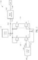
- FIG. 1 shows a reference voltage generator according to one embodiment of the present invention.
- FIG. 2 shows a timing diagram of the control signals generated by the control circuit.
- FIG. 3 shows a reference voltage generator according to another embodiment of the present invention.
- FIG. 4 shows a method for operating the reference voltage generators in FIG. 1 .
- FIG. 1 shows a reference voltage generator 100 according to one embodiment of the present invention.
- the reference voltage generator 100 includes an output terminal OUT, a current source 110 , a reference circuit 120 , a protection circuit 130 , and a control circuit 140 .
- the current source 110 is coupled to the output terminal OUT, and can generate a reference current I ref .
- the reference circuit 120 is coupled to the output terminal OUT.
- the reference circuit 120 includes N-type transistors N 1 A and N 2 A.
- the N-type transistor N 1 A has a first terminal coupled to the output terminal OUT, a second terminal, and a control terminal coupled to the first terminal of the N-type transistor N 1 A.
- the N-type transistor N 2 A has a first terminal coupled to the second terminal of the N-type transistor N 1 A, a second terminal for receiving a system voltage VS 1 , and a control terminal coupled to a first output terminal of the control circuit 140 .
- the reference circuit 120 can generate a reference voltage V ref according to the reference current I ref , and output the reference voltage V ref through the output terminal OUT.
- the output terminal OUT can be coupled to a sense amplifier SA 1 , and the sense amplifier SA 1 can compare the reference voltage V ref and a reading voltage V read .
- the reading voltage V read can be generated according to a reading current generated by the memory cell MC 1 . That is, the reference voltage V ref and the reading voltage V read can be designated to represent the reference current I ref and the reading current generated by the memory cell MC 1 .
- the reference current I ref generated by the current source 110 can be determined according to the characteristics of the memory cell MC 1 , therefore, the comparing result obtained by the sense amplifier SA 1 can be used to indicate the programming state of the memory cell MC 1 .
- the reference voltage generator 100 can be adopted in other application according to the system requirement.
- the sense amplifier SA 1 may compare the reading current generated by the memory cell MC 1 and the reference current I ref to determine the programming state of the memory cell MC 1 .
- the voltage of the output terminal OUT may be raised to a high level during the operations.
- the reference circuit 120 when the reference circuit 120 is enabled to generate the reference voltage V ref , the N-type transistor N 1 A of the reference circuit 120 may endure the hot carrier stress, and the reference voltage V ref may be shifted to a higher level than expected, causing errors to the system.
- the protection circuit 130 can be used to reduce the hot carrier stress.
- the protection circuit 130 can be coupled to the output terminal OUT, and can adjust the voltage of the output terminal OUT to an operating voltage V OPT before the reference circuit 120 is enabled.
- the protection circuit 130 includes N-type transistors N 3 A and N 4 A.
- the N-type transistor N 3 A has a first terminal coupled to the output terminal OUT, a second terminal, and a control terminal coupled to the first terminal of the N-type transistor N 3 A.
- the N-type transistor N 4 A has a first terminal coupled to the second terminal of the N-type transistor N 3 A, a second terminal for receiving the system voltage VS 1 , and a control terminal coupled to a second output terminal of the control circuit 140 .
- control circuit 140 can be coupled to the reference circuit 120 and the protection circuit 130 .
- control circuit 140 can generate control signals SIG ctrl1 and SIG ctrl2 through two output terminals for controlling the reference circuit 120 and the protection circuit 130 respectively.
- FIG. 2 shows a timing diagram of the control signals generated by the control circuit 140 .
- the control circuit 140 when the control circuit 140 receives a start signal SIG start , it may imply that the reference voltage V ref is required by the system. Therefore, when the control circuit 140 receives a start signal SIG start , the control circuit 140 can issue the control signal SIG ctr2 at a high voltage to the control terminal of the N-type transistor N 4 A. Therefore, the N-type transistor N 4 A would be turned on, and the protection circuit 130 can be enabled to adjust the voltage of the output terminal OUT to the operating voltage V OPT .
- the voltage of the output terminal OUT would be pulled down to the operating voltage V OPT from the high voltage VDD.
- the output terminal OUT may be at the high voltage VDD of 5V in the beginning, and will be pulled down to the operating voltage V OPT at 1.3V after the protection circuit 130 is enabled.
- the control circuit 140 can issue the control signal SIG ctr1 at a high voltage to the control terminal of the N-type transistor N 2 A. Therefore, the N-type transistor N 2 A would be turned on, and the reference circuit 120 can be enabled to generate the reference voltage V ref . Since the voltage of the output terminal OUT has been pulled down by the protection circuit 130 , the reference circuit 120 can adjust the voltage of the output terminal OUT from the operation voltage V OPT to the reference voltage V ref , for example but not limited to 1.2V, without suffering from the high voltage stress. Also, to ensure the accuracy of the reference voltage V ref generated by the reference circuit 120 , the control circuit 140 can disable the protection circuit 130 simultaneously when enabling the reference circuit 120 .
- the output terminal OUT can be discharged to a lower level by the protection circuit 130 . Consequently, the hot carrier stress applied on the reference circuit 120 can be reduced, and the accuracy of the reference voltage generator 100 can be improved.
- the sizes of the N-type transistors N 3 A and N 4 A can be greater than sizes of the N-type transistors N 1 A and N 2 A for improving the stability.
- the protection circuit 130 since the protection circuit 130 only needs to discharge the output terminal OUT to a rather low operation voltage V OPT for reducing the stress, the accuracy of the protection circuit 130 may not be critical.
- the sizes of the N-type transistors N 3 A and N 4 A can also be chosen to be smaller than sizes of the N-type transistors N 1 A and N 2 A for meeting the strict requirement of area.
- the reference circuit 120 and the protection circuit 130 can be implemented by N-type transistors in FIG. 1 , the reference circuit and the protection circuit may also be implemented with P-type transistors for generating a higher reference voltage in some other embodiments.
- FIG. 3 shows a reference voltage generator 200 according to another embodiment of the present invention.
- the reference voltage generator 200 and the reference voltage generator 100 have similar structures and can be operated with similar principles.
- the reference voltage generator 200 includes a current source 210 , a reference circuit 220 , a protection circuit 230 , and a control circuit 240 .
- the reference circuit 220 and the protection circuit 230 can be implemented with P-type transistors.
- the reference circuit 220 includes P-type transistor P 1 A and P 2 A.
- the P-type transistor P 1 A has a first terminal for receiving a system voltage VS 2 , a second terminal, and a control terminal coupled to a first output terminal of the control circuit 240 .
- the P-type transistor P 2 A has a first terminal coupled to the second terminal of the P-type transistor P 1 A, a second terminal coupled to the output terminal OUT, and a control terminal coupled to the second terminal of the P-type transistor P 2 A.
- the protection circuit 230 includes P-type transistors P 3 A and P 4 A.
- the P-type transistor P 3 A has a first terminal for receiving the system voltage VS 2 , a second terminal, and a control terminal coupled to a second output terminal of the control circuit 240 .
- the P-type transistor P 4 A has a first terminal coupled to the second terminal of the P-type transistor P 3 A, a second terminal coupled to the output terminal OUT, and a control terminal coupled to the second terminal of the P-type transistor P 4 A.
- the reference generator 200 may be used to generate a higher reference voltage V ref , for example but not limited to 3.8V, and the system voltage VS 2 can be, for example but not limited to 5V.
- V ref a higher reference voltage
- the system voltage VS 2 can be, for example but not limited to 5V.
- the P-type transistor P 2 A may endure a high voltage stress when the reference circuit 220 is enabled to generate the reference voltage V ref .
- the control circuit 240 may generate the control signal SIG ctrl2 at a low voltage to turn on the P-type transistor P 3 A so the protection circuit 230 will be enabled first to raise the voltage of the output terminal OUT to the operation voltage V OPT from the low voltage, for example, the ground voltage.
- the operation voltage V OPT can be, for example but not limited to 3.7V.
- the reference circuit 220 can adjust the voltage of the output terminal OUT from the operation voltage V OPT to the reference voltage V ref without suffering from the high voltage stress.
- the output terminal OUT can be charged to a higher level by the protection circuit 230 , reducing the hot carrier stress applied on the reference circuit 220 and improving the accuracy of the reference voltage generator 200 .
- the sizes of the P-type transistors P 3 A and P 4 A can be chosen to be greater or smaller than sizes of the P-type transistors P 1 A and P 2 A for the aforementioned reasons.
- FIG. 4 shows a method 300 for operating the reference voltage generators 100 .
- the method 300 includes steps S 310 to S 340 .
- steps S 330 and S 340 can be performed simultaneously. That is, the protection circuit 130 can be disabled as the reference circuit 120 is enabled.
- the method 300 can also be used to operate the reference voltage generator 200 .
- the reference voltage generator and the method for operating the reference voltage generator provided by the embodiments of the present invention can enable the protection circuit to adjust the voltage of the output terminal before the reference circuit is enabled; therefore, the hot carrier stress applied on the reference circuit can be reduced and the accuracy of reference voltage provided by the reference voltage generator can be improved.
Landscapes
- Engineering & Computer Science (AREA)
- Microelectronics & Electronic Packaging (AREA)
- Physics & Mathematics (AREA)
- Power Engineering (AREA)
- Automation & Control Theory (AREA)
- Electromagnetism (AREA)
- General Physics & Mathematics (AREA)
- Radar, Positioning & Navigation (AREA)
- Nonlinear Science (AREA)
- Computer Hardware Design (AREA)
- Read Only Memory (AREA)
- Control Of Electrical Variables (AREA)
- General Engineering & Computer Science (AREA)
- Non-Volatile Memory (AREA)
- Semiconductor Memories (AREA)
- Semiconductor Integrated Circuits (AREA)
Abstract
Description
Claims (4)
Priority Applications (3)
| Application Number | Priority Date | Filing Date | Title |
|---|---|---|---|
| US16/558,144 US11086349B2 (en) | 2018-11-16 | 2019-09-01 | Reference voltage generator capable of reducing hot carrier stress |
| TW108138051A TWI722612B (en) | 2018-11-16 | 2019-10-22 | Reference voltage generator and method for operating a reference voltage generator |
| CN201911049872.6A CN111198589B (en) | 2018-11-16 | 2019-10-31 | Reference voltage generator and operation method thereof |
Applications Claiming Priority (2)
| Application Number | Priority Date | Filing Date | Title |
|---|---|---|---|
| US201862768099P | 2018-11-16 | 2018-11-16 | |
| US16/558,144 US11086349B2 (en) | 2018-11-16 | 2019-09-01 | Reference voltage generator capable of reducing hot carrier stress |
Publications (2)
| Publication Number | Publication Date |
|---|---|
| US20200159273A1 US20200159273A1 (en) | 2020-05-21 |
| US11086349B2 true US11086349B2 (en) | 2021-08-10 |
Family
ID=70726482
Family Applications (7)
| Application Number | Title | Priority Date | Filing Date |
|---|---|---|---|
| US16/553,244 Active US10748607B2 (en) | 2018-11-16 | 2019-08-28 | Non-volatile memory device and associated peripheral circuit with data verifying and rewriting functions |
| US16/558,144 Active US11086349B2 (en) | 2018-11-16 | 2019-09-01 | Reference voltage generator capable of reducing hot carrier stress |
| US16/563,959 Active US10847218B2 (en) | 2018-11-16 | 2019-09-09 | Band-gap reference start-up circuit with greater noise margin for start-up |
| US16/581,838 Active US10803931B2 (en) | 2018-11-16 | 2019-09-25 | Non-volatile memory having memory array with differential cells |
| US16/592,951 Active US10783960B2 (en) | 2018-11-16 | 2019-10-04 | Non-volatile memory cell and non-volatile cell array |
| US16/658,179 Active US10916302B2 (en) | 2018-11-16 | 2019-10-21 | Method for operating a non-volatile memory cell |
| US17/134,471 Active US11004505B1 (en) | 2018-11-16 | 2020-12-27 | Method for operating a non-volatile memory cell |
Family Applications Before (1)
| Application Number | Title | Priority Date | Filing Date |
|---|---|---|---|
| US16/553,244 Active US10748607B2 (en) | 2018-11-16 | 2019-08-28 | Non-volatile memory device and associated peripheral circuit with data verifying and rewriting functions |
Family Applications After (5)
| Application Number | Title | Priority Date | Filing Date |
|---|---|---|---|
| US16/563,959 Active US10847218B2 (en) | 2018-11-16 | 2019-09-09 | Band-gap reference start-up circuit with greater noise margin for start-up |
| US16/581,838 Active US10803931B2 (en) | 2018-11-16 | 2019-09-25 | Non-volatile memory having memory array with differential cells |
| US16/592,951 Active US10783960B2 (en) | 2018-11-16 | 2019-10-04 | Non-volatile memory cell and non-volatile cell array |
| US16/658,179 Active US10916302B2 (en) | 2018-11-16 | 2019-10-21 | Method for operating a non-volatile memory cell |
| US17/134,471 Active US11004505B1 (en) | 2018-11-16 | 2020-12-27 | Method for operating a non-volatile memory cell |
Country Status (3)
| Country | Link |
|---|---|
| US (7) | US10748607B2 (en) |
| CN (4) | CN111199757B (en) |
| TW (7) | TWI708253B (en) |
Cited By (1)
| Publication number | Priority date | Publication date | Assignee | Title |
|---|---|---|---|---|
| US12444461B2 (en) | 2022-08-30 | 2025-10-14 | Samsung Electronics Co., Ltd. | SRAM including reference voltage generator and read method thereof |
Families Citing this family (8)
| Publication number | Priority date | Publication date | Assignee | Title |
|---|---|---|---|---|
| US11393534B2 (en) | 2020-05-28 | 2022-07-19 | Micron Technology, Inc. | Adjustment of a starting voltage corresponding to a program operation in a memory sub-system |
| US11867571B2 (en) * | 2021-10-01 | 2024-01-09 | Nxp B.V. | Self-turn-on temperature detector circuit |
| WO2023108383A1 (en) * | 2021-12-14 | 2023-06-22 | Yangtze Memory Technologies Co., Ltd. | Memory device and operation thereof |
| US11972800B2 (en) * | 2021-12-16 | 2024-04-30 | Ememory Technology Inc. | Non-volatile memory cell and non-volatile memory cell array |
| US12283326B2 (en) * | 2022-03-11 | 2025-04-22 | Ememory Technology Inc. | Memory cell and array structure of non-volatile memory and associated control method |
| US11901004B2 (en) * | 2022-04-08 | 2024-02-13 | Taiwan Semiconductor Manufacturing Company, Ltd. | Memory array, memory structure and operation method of memory array |
| US12526986B2 (en) * | 2023-05-24 | 2026-01-13 | Ememory Technology Inc. | Non-volatile memory cell of array structure and associated controlling method |
| US12554433B2 (en) * | 2023-11-26 | 2026-02-17 | Taiwan Semiconductor Manufacturing Company, Ltd. | Memory device |
Citations (49)
| Publication number | Priority date | Publication date | Assignee | Title |
|---|---|---|---|---|
| US5132936A (en) | 1989-12-14 | 1992-07-21 | Cypress Semiconductor Corporation | MOS memory circuit with fast access time |
| US5369312A (en) | 1991-10-08 | 1994-11-29 | Hyundai Electronics Industries Co., Ltd. | Hot carrier protection circuit |
| US6016050A (en) * | 1998-07-07 | 2000-01-18 | Analog Devices, Inc. | Start-up and bias circuit |
| US20020033720A1 (en) * | 2000-09-21 | 2002-03-21 | Tamio Ikehashi | Semiconductor device |
| US6400212B1 (en) | 1999-07-13 | 2002-06-04 | National Semiconductor Corporation | Apparatus and method for reference voltage generator with self-monitoring |
| US20030057931A1 (en) * | 2001-08-28 | 2003-03-27 | Ercole Di Iorio | Ultra low power tracked low voltage reference source |
| WO2003049289A1 (en) | 2001-12-03 | 2003-06-12 | Broadcom Corporation | Hot carrier injection suppression circuit |
| US6584019B1 (en) * | 1999-07-01 | 2003-06-24 | Micron Technology, Inc. | Leakage detection in flash memory cell |
| TW574782B (en) | 2002-04-30 | 2004-02-01 | Realtek Semiconductor Corp | Fast start-up low-voltage bandgap voltage reference circuit |
| US20050286305A1 (en) | 2004-06-29 | 2005-12-29 | Samsung Electronics Co., Ltd. | Sensing circuit for flash memory device operating at low power supply voltage |
| US20060114054A1 (en) * | 2004-11-30 | 2006-06-01 | Hari Giduturi | Voltage reference apparatus, method, and system |
| US20060132114A1 (en) * | 2004-12-21 | 2006-06-22 | Hari Giduturi | Step voltage generation |
| US20070052405A1 (en) * | 2005-09-07 | 2007-03-08 | Toshio Mochizuki | Reference voltage generating circuit, a semiconductor integrated circuit and a semiconductor integrated circuit apparatus |
| TW200812246A (en) | 2006-08-18 | 2008-03-01 | Elite Semiconductor Esmt | Low power reference voltage circuit |
| US7342390B2 (en) | 2006-05-01 | 2008-03-11 | Fujitsu Limited | Reference voltage generation circuit |
| US20080106965A1 (en) * | 2006-11-07 | 2008-05-08 | Nec Electronics Corporation | Semiconductor device and memory |
| US20080239837A1 (en) * | 2006-09-26 | 2008-10-02 | Noriyasu Kumazaki | Semiconductor device |
| US20090016106A1 (en) * | 2007-07-13 | 2009-01-15 | Silicon Storage Technology, Inc. | Sub volt flash memory system |
| US20090033355A1 (en) | 2007-08-02 | 2009-02-05 | International Business Machines Corporation | Method And Apparatus To Measure Threshold Shifting Of A MOSFET Device And Voltage Difference Between Nodes |
| US20090146624A1 (en) * | 2007-12-11 | 2009-06-11 | Kim Han-Su | Shunt regulator having over-voltage protection circuit and semiconductor device including the same |
| CN101515476A (en) | 2008-02-22 | 2009-08-26 | 精工电子有限公司 | Nonvolatile semiconductor memory device |
| US20090257288A1 (en) * | 2008-04-11 | 2009-10-15 | Roohparvar Frankie F | Apparatus and method for increasing data line noise tolerance |
| US20090256625A1 (en) | 2008-04-15 | 2009-10-15 | Tae Hyung Jung | Circuit and method for a gate control circuit with reduced voltage stress |
| CN100570527C (en) | 2006-06-16 | 2009-12-16 | 义隆电子股份有限公司 | Reference voltage generation circuit |
| US20100052636A1 (en) * | 2008-08-29 | 2010-03-04 | Ricoh Company, Ltd. | Constant-voltage circuit device |
| US20110234289A1 (en) | 2005-12-07 | 2011-09-29 | Vivek Subramanian | Process-Variation Tolerant Diode, Standard Cells Including the Same, Tags and Sensors Containing the Same, and Methods for Manufacturing the Same |
| CN102375470A (en) | 2010-08-20 | 2012-03-14 | 张伟 | Band gap reference voltage circuit |
| TW201243534A (en) | 2011-02-16 | 2012-11-01 | Mediatek Singapore Pte Ltd | Regulator providing various output voltages |
| CN103117080A (en) | 2013-02-01 | 2013-05-22 | 上海宏力半导体制造有限公司 | Reading circuit |
| CN103117741A (en) | 2011-11-16 | 2013-05-22 | 国民技术股份有限公司 | Bias current generation circuit and tail current source circuit |
| US20130154605A1 (en) * | 2011-12-20 | 2013-06-20 | Ricoh Company, Ltd. | Constant voltage circuit and electronic device including same |
| CN203135827U (en) | 2012-12-31 | 2013-08-14 | 意法半导体研发(深圳)有限公司 | Drive circuit used for driving power transistor |
| US20130335043A1 (en) * | 2010-11-09 | 2013-12-19 | Tdk-Lambda Corporation | Multi-level voltage regulator system and method |
| CN103595024A (en) | 2012-12-24 | 2014-02-19 | 极创电子股份有限公司 | Protection circuit of power supply |
| US20140077788A1 (en) * | 2012-09-14 | 2014-03-20 | Nxp B.V. | Shunt regulator |
| WO2014101837A1 (en) | 2012-12-28 | 2014-07-03 | 电子科技大学 | Multipath current source switching device |
| CN203786597U (en) | 2014-04-30 | 2014-08-20 | 杭州士兰微电子股份有限公司 | Low-dropout linear regulator |
| CN104571241A (en) | 2013-10-09 | 2015-04-29 | 盛群半导体股份有限公司 | Voltage stabilizing circuit and method thereof |
| CN104850161A (en) | 2014-02-18 | 2015-08-19 | 台湾积体电路制造股份有限公司 | Flipped gate voltage reference and method of using |
| US20150255162A1 (en) * | 2014-03-10 | 2015-09-10 | Kabushiki Kaisha Toshiba | Semiconductor memory device and method for detecting leak current |
| US9153335B2 (en) * | 2013-08-20 | 2015-10-06 | Winbond Electronics Corp. | Clamp voltage generator of a semiconductor memory apparatus |
| CN104979000A (en) | 2014-04-09 | 2015-10-14 | 力旺电子股份有限公司 | Sensing device and data sensing method thereof |
| US9189007B2 (en) | 2011-03-10 | 2015-11-17 | Taiwan Semiconductor Manufacturing Company, Ltd. | Power supply regulator |
| US9618959B2 (en) | 2013-09-12 | 2017-04-11 | Texas Instruments Incorporated | Reference generator circuit with dynamically tracking threshold |
| US20170178745A1 (en) * | 2015-02-25 | 2017-06-22 | Ememory Technology Inc. | One time programmable non-volatile memory and read sensing method thereof |
| US9720435B2 (en) | 2015-12-28 | 2017-08-01 | Adtran, Inc. | Reference current source |
| US10062448B1 (en) * | 2017-11-07 | 2018-08-28 | Texas Instruments Incorporated | Zero bias fuse cell |
| US20180268898A1 (en) | 2017-03-16 | 2018-09-20 | Toshiba Memory Corporation | Non-volatile semiconductor memory device |
| US20180323780A1 (en) | 2017-05-02 | 2018-11-08 | Richwave Technology Corp. | Bandgap reference circuit having clamping control circuit and being capable of improving rate of providing predetermined voltage |
Family Cites Families (61)
| Publication number | Priority date | Publication date | Assignee | Title |
|---|---|---|---|---|
| FR2728380A1 (en) * | 1994-12-20 | 1996-06-21 | Sgs Thomson Microelectronics | METHOD FOR WRITING DATA IN A CORRESPONDING ELECTRICALLY PROGRAMMABLE MEMORY AND MEMORY |
| WO1997030454A1 (en) * | 1996-02-19 | 1997-08-21 | Citizen Watch Co., Ltd. | Semiconductor nonvolatile memory |
| EP0904588B1 (en) * | 1996-06-14 | 2001-07-25 | Infineon Technologies AG | A device and method for multi-level charge/storage and reading out |
| US5867013A (en) * | 1997-11-20 | 1999-02-02 | Cypress Semiconductor Corporation | Startup circuit for band-gap reference circuit |
| JP3166838B2 (en) * | 1997-12-16 | 2001-05-14 | 日本電気株式会社 | Priority encoder and priority encoding method |
| US6201435B1 (en) * | 1999-08-26 | 2001-03-13 | Taiwan Semiconductor Manufacturing Company | Low-power start-up circuit for a reference voltage generator |
| US6259240B1 (en) * | 2000-05-19 | 2001-07-10 | Agere Systems Guardian Corp. | Power-up circuit for analog circuit |
| US6349056B1 (en) * | 2000-12-28 | 2002-02-19 | Sandisk Corporation | Method and structure for efficient data verification operation for non-volatile memories |
| JP3678692B2 (en) | 2001-10-26 | 2005-08-03 | 沖電気工業株式会社 | Bandgap reference voltage circuit |
| US6920067B2 (en) | 2002-12-25 | 2005-07-19 | Ememory Technology Inc. | Integrated circuit embedded with single-poly non-volatile memory |
| JP4005000B2 (en) * | 2003-07-04 | 2007-11-07 | 株式会社東芝 | Semiconductor memory device and data writing method. |
| US6879142B2 (en) * | 2003-08-20 | 2005-04-12 | Broadcom Corporation | Power management unit for use in portable applications |
| US7209392B2 (en) | 2004-07-20 | 2007-04-24 | Ememory Technology Inc. | Single poly non-volatile memory |
| US7388250B2 (en) * | 2004-08-13 | 2008-06-17 | United Microelectronics Corp. | Non-volatile memory cell and manufacturing method thereof |
| JP4712365B2 (en) * | 2004-08-13 | 2011-06-29 | ルネサスエレクトロニクス株式会社 | Nonvolatile semiconductor memory device and semiconductor memory device |
| GB2436272B (en) * | 2005-01-27 | 2011-01-19 | Spansion Llc | Semiconductor device, address assignment method, and verify method |
| KR100739967B1 (en) * | 2005-05-27 | 2007-07-16 | 주식회사 하이닉스반도체 | Program method of flash memory device |
| US7656710B1 (en) | 2005-07-14 | 2010-02-02 | Sau Ching Wong | Adaptive operations for nonvolatile memories |
| CN1928766A (en) * | 2005-09-07 | 2007-03-14 | 株式会社瑞萨科技 | Reference voltage generating circuit, a semiconductor integrated circuit and a semiconductor integrated circuit apparatus |
| US7755419B2 (en) * | 2006-01-17 | 2010-07-13 | Cypress Semiconductor Corporation | Low power beta multiplier start-up circuit and method |
| WO2007090089A2 (en) | 2006-01-27 | 2007-08-09 | Kilopass Technology, Inc. | Electrically programmable fuse bit |
| KR100706816B1 (en) * | 2006-03-10 | 2007-04-12 | 삼성전자주식회사 | Nonvolatile memory device and its programming method which can improve program speed |
| US20090003074A1 (en) * | 2006-03-30 | 2009-01-01 | Catalyst Semiconductor, Inc. | Scalable Electrically Eraseable And Programmable Memory (EEPROM) Cell Array |
| US7428172B2 (en) | 2006-07-17 | 2008-09-23 | Freescale Semiconductor, Inc. | Concurrent programming and program verification of floating gate transistor |
| US20080158986A1 (en) | 2006-12-29 | 2008-07-03 | Daniel Elmhurst | Flash memory and associated methods |
| US7659705B2 (en) * | 2007-03-16 | 2010-02-09 | Smartech Worldwide Limited | Low-power start-up circuit for bandgap reference voltage generator |
| US7679352B2 (en) * | 2007-05-30 | 2010-03-16 | Faraday Technology Corp. | Bandgap reference circuits |
| KR100891405B1 (en) * | 2007-09-27 | 2009-04-02 | 주식회사 하이닉스반도체 | Nonvolatile Memory Device and Its Operation Method |
| KR100953046B1 (en) * | 2007-12-27 | 2010-04-14 | 주식회사 하이닉스반도체 | Operation method of nonvolatile memory device |
| US7956597B2 (en) * | 2008-06-24 | 2011-06-07 | Mediatek Inc. | Reference buffer circuits for providing reference voltages |
| US7983078B2 (en) | 2008-09-24 | 2011-07-19 | Sandisk Technologies Inc. | Data retention of last word line of non-volatile memory arrays |
| KR101642465B1 (en) * | 2008-12-12 | 2016-07-25 | 삼성전자주식회사 | Access method of non-volatile memory device |
| KR20100077271A (en) * | 2008-12-29 | 2010-07-08 | 주식회사 동부하이텍 | Reference voltage generation circuit |
| KR101585958B1 (en) * | 2008-12-29 | 2016-01-18 | 주식회사 동부하이텍 | Reference voltage generation circuit |
| KR101532584B1 (en) | 2009-01-30 | 2015-06-30 | 삼성전자주식회사 | Multi-level non-volatile semiconductor device, memory system having the same and Operating method there-of |
| TWI380154B (en) | 2009-04-16 | 2012-12-21 | Vanguard Int Semiconduct Corp | Bandgap reference circuits |
| US7940554B2 (en) * | 2009-04-24 | 2011-05-10 | Sandisk 3D Llc | Reduced complexity array line drivers for 3D matrix arrays |
| EP2273339A1 (en) * | 2009-07-08 | 2011-01-12 | Dialog Semiconductor GmbH | Startup circuit for bandgap voltage reference generators |
| KR101676816B1 (en) | 2010-02-11 | 2016-11-18 | 삼성전자주식회사 | Flash memory device and program method thereof |
| KR101771619B1 (en) * | 2011-02-09 | 2017-08-28 | 삼성전자주식회사 | Nonvolatile memory device and driving method thereof |
| US8363477B2 (en) * | 2011-03-09 | 2013-01-29 | Ememory Technology Inc. | Method of setting trim codes for a flash memory and related device |
| TWI444813B (en) | 2011-03-16 | 2014-07-11 | Himax Tech Ltd | Bandgap circuit and start circuit thereof |
| KR101298190B1 (en) * | 2011-10-13 | 2013-08-20 | 에스케이하이닉스 주식회사 | Resistive Memory Apparatus, Layout Structure and Sensing Circuit Thereof |
| CN105932972B (en) * | 2012-03-22 | 2019-01-15 | 联咏科技股份有限公司 | output stage circuit |
| JP5942781B2 (en) * | 2012-04-16 | 2016-06-29 | ソニー株式会社 | Storage control device, memory system, information processing system, and storage control method |
| US8995202B2 (en) * | 2012-05-21 | 2015-03-31 | Freescale Semiconductor, Inc. | Test flow to detect a latent leaky bit of a non-volatile memory |
| US9142315B2 (en) * | 2012-07-25 | 2015-09-22 | Freescale Semiconductor, Inc. | Methods and systems for adjusting NVM cell bias conditions for read/verify operations to compensate for performance degradation |
| KR20140104203A (en) * | 2013-02-20 | 2014-08-28 | 삼성전자주식회사 | Circuit for generating reference voltage |
| US9515152B2 (en) * | 2013-06-27 | 2016-12-06 | Globalfoundries Singapore Pte. Ltd. | Simple and cost-free MTP structure |
| US9019780B1 (en) * | 2013-10-08 | 2015-04-28 | Ememory Technology Inc. | Non-volatile memory apparatus and data verification method thereof |
| KR20150142503A (en) * | 2014-06-12 | 2015-12-22 | 에스케이하이닉스 주식회사 | Semiconductor device and operating method thereof |
| US9627088B2 (en) * | 2015-02-25 | 2017-04-18 | Ememory Technology Inc. | One time programmable non-volatile memory and read sensing method thereof |
| US9502426B1 (en) | 2015-07-06 | 2016-11-22 | Ememory Technology Inc. | One time programming non-volatile memory cell |
| US9710010B2 (en) | 2015-07-10 | 2017-07-18 | Sk Hynix Memory Solutions Inc. | Start-up circuit for bandgap reference |
| US9548124B1 (en) | 2015-10-14 | 2017-01-17 | Sandisk Technologies Llc | Word line dependent programming in a memory device |
| US9847133B2 (en) | 2016-01-19 | 2017-12-19 | Ememory Technology Inc. | Memory array capable of performing byte erase operation |
| US9881693B2 (en) * | 2016-02-16 | 2018-01-30 | Micron Technology, Inc. | Selectors on interface die for memory device |
| US9852800B2 (en) | 2016-03-07 | 2017-12-26 | Sandisk Technologies Llc | Adaptive determination of program parameter using program of erase rate |
| US10090027B2 (en) | 2016-05-25 | 2018-10-02 | Ememory Technology Inc. | Memory system with low read power |
| US9922992B1 (en) | 2017-04-10 | 2018-03-20 | Sandisk Technologies Llc | Doping channels of edge cells to provide uniform programming speed and reduce read disturb |
| US10510426B2 (en) * | 2018-04-27 | 2019-12-17 | Gigadevice Semiconductor (Shanghai) Inc. | Programming method, programming apparatus and storage medium for non-volatile memory |
-
2019
- 2019-07-18 TW TW108125501A patent/TWI708253B/en active
- 2019-08-28 US US16/553,244 patent/US10748607B2/en active Active
- 2019-09-01 US US16/558,144 patent/US11086349B2/en active Active
- 2019-09-09 US US16/563,959 patent/US10847218B2/en active Active
- 2019-09-25 US US16/581,838 patent/US10803931B2/en active Active
- 2019-09-27 TW TW108135057A patent/TWI712039B/en active
- 2019-10-04 US US16/592,951 patent/US10783960B2/en active Active
- 2019-10-14 CN CN201910971827.XA patent/CN111199757B/en active Active
- 2019-10-21 US US16/658,179 patent/US10916302B2/en active Active
- 2019-10-21 TW TW108137897A patent/TWI706412B/en active
- 2019-10-22 TW TW108138051A patent/TWI722612B/en active
- 2019-10-23 TW TW108138138A patent/TWI711251B/en active
- 2019-10-23 TW TW108138309A patent/TWI715263B/en active
- 2019-10-29 TW TW108138937A patent/TWI715270B/en active
- 2019-10-31 CN CN201911049872.6A patent/CN111198589B/en active Active
- 2019-10-31 CN CN201911049855.2A patent/CN111221370B/en active Active
- 2019-11-12 CN CN201911102513.2A patent/CN111199763B/en active Active
-
2020
- 2020-12-27 US US17/134,471 patent/US11004505B1/en active Active
Patent Citations (54)
| Publication number | Priority date | Publication date | Assignee | Title |
|---|---|---|---|---|
| US5132936A (en) | 1989-12-14 | 1992-07-21 | Cypress Semiconductor Corporation | MOS memory circuit with fast access time |
| US5369312A (en) | 1991-10-08 | 1994-11-29 | Hyundai Electronics Industries Co., Ltd. | Hot carrier protection circuit |
| US6016050A (en) * | 1998-07-07 | 2000-01-18 | Analog Devices, Inc. | Start-up and bias circuit |
| US6584019B1 (en) * | 1999-07-01 | 2003-06-24 | Micron Technology, Inc. | Leakage detection in flash memory cell |
| US6400212B1 (en) | 1999-07-13 | 2002-06-04 | National Semiconductor Corporation | Apparatus and method for reference voltage generator with self-monitoring |
| US20020033720A1 (en) * | 2000-09-21 | 2002-03-21 | Tamio Ikehashi | Semiconductor device |
| US20030057931A1 (en) * | 2001-08-28 | 2003-03-27 | Ercole Di Iorio | Ultra low power tracked low voltage reference source |
| WO2003049289A1 (en) | 2001-12-03 | 2003-06-12 | Broadcom Corporation | Hot carrier injection suppression circuit |
| TW574782B (en) | 2002-04-30 | 2004-02-01 | Realtek Semiconductor Corp | Fast start-up low-voltage bandgap voltage reference circuit |
| US20050286305A1 (en) | 2004-06-29 | 2005-12-29 | Samsung Electronics Co., Ltd. | Sensing circuit for flash memory device operating at low power supply voltage |
| CN1725381A (en) | 2004-06-29 | 2006-01-25 | 三星电子株式会社 | Readout circuit for flash memory devices operating at low supply voltage |
| US20060114054A1 (en) * | 2004-11-30 | 2006-06-01 | Hari Giduturi | Voltage reference apparatus, method, and system |
| US20060132114A1 (en) * | 2004-12-21 | 2006-06-22 | Hari Giduturi | Step voltage generation |
| US20070052405A1 (en) * | 2005-09-07 | 2007-03-08 | Toshio Mochizuki | Reference voltage generating circuit, a semiconductor integrated circuit and a semiconductor integrated circuit apparatus |
| US20110234289A1 (en) | 2005-12-07 | 2011-09-29 | Vivek Subramanian | Process-Variation Tolerant Diode, Standard Cells Including the Same, Tags and Sensors Containing the Same, and Methods for Manufacturing the Same |
| US7342390B2 (en) | 2006-05-01 | 2008-03-11 | Fujitsu Limited | Reference voltage generation circuit |
| CN100570527C (en) | 2006-06-16 | 2009-12-16 | 义隆电子股份有限公司 | Reference voltage generation circuit |
| TW200812246A (en) | 2006-08-18 | 2008-03-01 | Elite Semiconductor Esmt | Low power reference voltage circuit |
| US20080239837A1 (en) * | 2006-09-26 | 2008-10-02 | Noriyasu Kumazaki | Semiconductor device |
| US20080106965A1 (en) * | 2006-11-07 | 2008-05-08 | Nec Electronics Corporation | Semiconductor device and memory |
| US20090016106A1 (en) * | 2007-07-13 | 2009-01-15 | Silicon Storage Technology, Inc. | Sub volt flash memory system |
| US20090033355A1 (en) | 2007-08-02 | 2009-02-05 | International Business Machines Corporation | Method And Apparatus To Measure Threshold Shifting Of A MOSFET Device And Voltage Difference Between Nodes |
| US20090146624A1 (en) * | 2007-12-11 | 2009-06-11 | Kim Han-Su | Shunt regulator having over-voltage protection circuit and semiconductor device including the same |
| US20090213665A1 (en) | 2008-02-22 | 2009-08-27 | Fumiyasu Utsunomiya | Nonvolatile semiconductor memory device |
| CN101515476A (en) | 2008-02-22 | 2009-08-26 | 精工电子有限公司 | Nonvolatile semiconductor memory device |
| US20090257288A1 (en) * | 2008-04-11 | 2009-10-15 | Roohparvar Frankie F | Apparatus and method for increasing data line noise tolerance |
| CN101594137A (en) | 2008-04-15 | 2009-12-02 | 台湾积体电路制造股份有限公司 | Circuit of grid control circuit with reduced voltage stress |
| US20090256625A1 (en) | 2008-04-15 | 2009-10-15 | Tae Hyung Jung | Circuit and method for a gate control circuit with reduced voltage stress |
| US20100052636A1 (en) * | 2008-08-29 | 2010-03-04 | Ricoh Company, Ltd. | Constant-voltage circuit device |
| CN102375470A (en) | 2010-08-20 | 2012-03-14 | 张伟 | Band gap reference voltage circuit |
| US20130335043A1 (en) * | 2010-11-09 | 2013-12-19 | Tdk-Lambda Corporation | Multi-level voltage regulator system and method |
| TW201243534A (en) | 2011-02-16 | 2012-11-01 | Mediatek Singapore Pte Ltd | Regulator providing various output voltages |
| US9189007B2 (en) | 2011-03-10 | 2015-11-17 | Taiwan Semiconductor Manufacturing Company, Ltd. | Power supply regulator |
| CN103117741A (en) | 2011-11-16 | 2013-05-22 | 国民技术股份有限公司 | Bias current generation circuit and tail current source circuit |
| US20130154605A1 (en) * | 2011-12-20 | 2013-06-20 | Ricoh Company, Ltd. | Constant voltage circuit and electronic device including same |
| US20140077788A1 (en) * | 2012-09-14 | 2014-03-20 | Nxp B.V. | Shunt regulator |
| CN103595024A (en) | 2012-12-24 | 2014-02-19 | 极创电子股份有限公司 | Protection circuit of power supply |
| WO2014101837A1 (en) | 2012-12-28 | 2014-07-03 | 电子科技大学 | Multipath current source switching device |
| CN203135827U (en) | 2012-12-31 | 2013-08-14 | 意法半导体研发(深圳)有限公司 | Drive circuit used for driving power transistor |
| CN103117080A (en) | 2013-02-01 | 2013-05-22 | 上海宏力半导体制造有限公司 | Reading circuit |
| US9153335B2 (en) * | 2013-08-20 | 2015-10-06 | Winbond Electronics Corp. | Clamp voltage generator of a semiconductor memory apparatus |
| US9618959B2 (en) | 2013-09-12 | 2017-04-11 | Texas Instruments Incorporated | Reference generator circuit with dynamically tracking threshold |
| CN104571241A (en) | 2013-10-09 | 2015-04-29 | 盛群半导体股份有限公司 | Voltage stabilizing circuit and method thereof |
| CN104850161A (en) | 2014-02-18 | 2015-08-19 | 台湾积体电路制造股份有限公司 | Flipped gate voltage reference and method of using |
| US20150234413A1 (en) * | 2014-02-18 | 2015-08-20 | Taiwan Semiconductor Manufacturing Company, Ltd. | Flipped gate voltage reference and method of using |
| US20150255162A1 (en) * | 2014-03-10 | 2015-09-10 | Kabushiki Kaisha Toshiba | Semiconductor memory device and method for detecting leak current |
| CN104979000A (en) | 2014-04-09 | 2015-10-14 | 力旺电子股份有限公司 | Sensing device and data sensing method thereof |
| CN203786597U (en) | 2014-04-30 | 2014-08-20 | 杭州士兰微电子股份有限公司 | Low-dropout linear regulator |
| US20170178745A1 (en) * | 2015-02-25 | 2017-06-22 | Ememory Technology Inc. | One time programmable non-volatile memory and read sensing method thereof |
| US9720435B2 (en) | 2015-12-28 | 2017-08-01 | Adtran, Inc. | Reference current source |
| US20180268898A1 (en) | 2017-03-16 | 2018-09-20 | Toshiba Memory Corporation | Non-volatile semiconductor memory device |
| CN108630270A (en) | 2017-03-16 | 2018-10-09 | 东芝存储器株式会社 | non-volatile semiconductor storage device |
| US20180323780A1 (en) | 2017-05-02 | 2018-11-08 | Richwave Technology Corp. | Bandgap reference circuit having clamping control circuit and being capable of improving rate of providing predetermined voltage |
| US10062448B1 (en) * | 2017-11-07 | 2018-08-28 | Texas Instruments Incorporated | Zero bias fuse cell |
Cited By (1)
| Publication number | Priority date | Publication date | Assignee | Title |
|---|---|---|---|---|
| US12444461B2 (en) | 2022-08-30 | 2025-10-14 | Samsung Electronics Co., Ltd. | SRAM including reference voltage generator and read method thereof |
Also Published As
Similar Documents
| Publication | Publication Date | Title |
|---|---|---|
| US11086349B2 (en) | Reference voltage generator capable of reducing hot carrier stress | |
| US6226224B1 (en) | Semiconductor integrated circuit device and storage device | |
| US9099191B2 (en) | Current sensing amplifier and sensing method thereof | |
| US6353559B2 (en) | Write circuit for a semiconductor memory device | |
| US7795848B2 (en) | Method and circuit for generating output voltages from input voltage | |
| US7751230B2 (en) | Negative voltage generating device | |
| US8514638B2 (en) | Write control circuit and semiconductor device | |
| US6590442B2 (en) | Voltage boosting circuit for an integrated circuit device | |
| US7969797B2 (en) | Semiconductor memory device and method for operating the same | |
| US7579821B2 (en) | Voltage generator | |
| US6351180B1 (en) | Clamp circuit with fuse options | |
| US20210167771A1 (en) | Power-on reset signal generating device | |
| US9343966B1 (en) | Voltage switching system for integrated circuit | |
| US9733655B2 (en) | Low dropout regulators with fast response speed for mode switching | |
| US6787938B1 (en) | Method and circuit for switchover between a primary and a secondary power source | |
| US20090237130A1 (en) | Dual power-up signal generator | |
| US6535425B2 (en) | Nonvolatile semiconductor memory device | |
| US10770118B2 (en) | Reverse bias voltage adjuster | |
| US11830557B2 (en) | Memory apparatus | |
| US20110001556A1 (en) | Integrated circuit | |
| US7768842B2 (en) | Semiconductor memory device voltage generating circuit for avoiding leakage currents of parasitic diodes | |
| US6515932B1 (en) | Memory circuit | |
| US20080238501A1 (en) | Initialization signal generating circuit | |
| US8884645B1 (en) | Semiconductor apparatus | |
| US9893612B2 (en) | Voltage generation circuit |
Legal Events
| Date | Code | Title | Description |
|---|---|---|---|
| FEPP | Fee payment procedure |
Free format text: ENTITY STATUS SET TO UNDISCOUNTED (ORIGINAL EVENT CODE: BIG.); ENTITY STATUS OF PATENT OWNER: SMALL ENTITY |
|
| FEPP | Fee payment procedure |
Free format text: ENTITY STATUS SET TO SMALL (ORIGINAL EVENT CODE: SMAL); ENTITY STATUS OF PATENT OWNER: SMALL ENTITY |
|
| STPP | Information on status: patent application and granting procedure in general |
Free format text: RESPONSE TO NON-FINAL OFFICE ACTION ENTERED AND FORWARDED TO EXAMINER |
|
| STPP | Information on status: patent application and granting procedure in general |
Free format text: DOCKETED NEW CASE - READY FOR EXAMINATION |
|
| STPP | Information on status: patent application and granting procedure in general |
Free format text: RESPONSE TO NON-FINAL OFFICE ACTION ENTERED AND FORWARDED TO EXAMINER |
|
| STPP | Information on status: patent application and granting procedure in general |
Free format text: NOTICE OF ALLOWANCE MAILED -- APPLICATION RECEIVED IN OFFICE OF PUBLICATIONS |
|
| STPP | Information on status: patent application and granting procedure in general |
Free format text: PUBLICATIONS -- ISSUE FEE PAYMENT RECEIVED |
|
| STPP | Information on status: patent application and granting procedure in general |
Free format text: PUBLICATIONS -- ISSUE FEE PAYMENT VERIFIED |
|
| STCF | Information on status: patent grant |
Free format text: PATENTED CASE |
|
| MAFP | Maintenance fee payment |
Free format text: PAYMENT OF MAINTENANCE FEE, 4TH YR, SMALL ENTITY (ORIGINAL EVENT CODE: M2551); ENTITY STATUS OF PATENT OWNER: SMALL ENTITY Year of fee payment: 4 |