US11061284B2 - Array substrate comprising electrode having parallel straight portions, display panel, and display device - Google Patents
Array substrate comprising electrode having parallel straight portions, display panel, and display device Download PDFInfo
- Publication number
- US11061284B2 US11061284B2 US15/993,154 US201815993154A US11061284B2 US 11061284 B2 US11061284 B2 US 11061284B2 US 201815993154 A US201815993154 A US 201815993154A US 11061284 B2 US11061284 B2 US 11061284B2
- Authority
- US
- United States
- Prior art keywords
- adjustment
- subpixel region
- electrode
- straight portions
- subpixel
- Prior art date
- Legal status (The legal status is an assumption and is not a legal conclusion. Google has not performed a legal analysis and makes no representation as to the accuracy of the status listed.)
- Active, expires
Links
Images


Classifications
-
- G—PHYSICS
- G02—OPTICS
- G02F—OPTICAL DEVICES OR ARRANGEMENTS FOR THE CONTROL OF LIGHT BY MODIFICATION OF THE OPTICAL PROPERTIES OF THE MEDIA OF THE ELEMENTS INVOLVED THEREIN; NON-LINEAR OPTICS; FREQUENCY-CHANGING OF LIGHT; OPTICAL LOGIC ELEMENTS; OPTICAL ANALOGUE/DIGITAL CONVERTERS
- G02F1/00—Devices or arrangements for the control of the intensity, colour, phase, polarisation or direction of light arriving from an independent light source, e.g. switching, gating or modulating; Non-linear optics
- G02F1/01—Devices or arrangements for the control of the intensity, colour, phase, polarisation or direction of light arriving from an independent light source, e.g. switching, gating or modulating; Non-linear optics for the control of the intensity, phase, polarisation or colour
- G02F1/13—Devices or arrangements for the control of the intensity, colour, phase, polarisation or direction of light arriving from an independent light source, e.g. switching, gating or modulating; Non-linear optics for the control of the intensity, phase, polarisation or colour based on liquid crystals, e.g. single liquid crystal display cells
- G02F1/133—Constructional arrangements; Operation of liquid crystal cells; Circuit arrangements
- G02F1/1333—Constructional arrangements; Manufacturing methods
- G02F1/1343—Electrodes
- G02F1/134309—Electrodes characterised by their geometrical arrangement
-
- G—PHYSICS
- G02—OPTICS
- G02F—OPTICAL DEVICES OR ARRANGEMENTS FOR THE CONTROL OF LIGHT BY MODIFICATION OF THE OPTICAL PROPERTIES OF THE MEDIA OF THE ELEMENTS INVOLVED THEREIN; NON-LINEAR OPTICS; FREQUENCY-CHANGING OF LIGHT; OPTICAL LOGIC ELEMENTS; OPTICAL ANALOGUE/DIGITAL CONVERTERS
- G02F1/00—Devices or arrangements for the control of the intensity, colour, phase, polarisation or direction of light arriving from an independent light source, e.g. switching, gating or modulating; Non-linear optics
- G02F1/01—Devices or arrangements for the control of the intensity, colour, phase, polarisation or direction of light arriving from an independent light source, e.g. switching, gating or modulating; Non-linear optics for the control of the intensity, phase, polarisation or colour
- G02F1/13—Devices or arrangements for the control of the intensity, colour, phase, polarisation or direction of light arriving from an independent light source, e.g. switching, gating or modulating; Non-linear optics for the control of the intensity, phase, polarisation or colour based on liquid crystals, e.g. single liquid crystal display cells
- G02F1/133—Constructional arrangements; Operation of liquid crystal cells; Circuit arrangements
- G02F1/1333—Constructional arrangements; Manufacturing methods
- G02F1/1337—Surface-induced orientation of the liquid crystal molecules, e.g. by alignment layers
- G02F1/133707—Structures for producing distorted electric fields, e.g. bumps, protrusions, recesses, slits in pixel electrodes
-
- G—PHYSICS
- G02—OPTICS
- G02F—OPTICAL DEVICES OR ARRANGEMENTS FOR THE CONTROL OF LIGHT BY MODIFICATION OF THE OPTICAL PROPERTIES OF THE MEDIA OF THE ELEMENTS INVOLVED THEREIN; NON-LINEAR OPTICS; FREQUENCY-CHANGING OF LIGHT; OPTICAL LOGIC ELEMENTS; OPTICAL ANALOGUE/DIGITAL CONVERTERS
- G02F1/00—Devices or arrangements for the control of the intensity, colour, phase, polarisation or direction of light arriving from an independent light source, e.g. switching, gating or modulating; Non-linear optics
- G02F1/01—Devices or arrangements for the control of the intensity, colour, phase, polarisation or direction of light arriving from an independent light source, e.g. switching, gating or modulating; Non-linear optics for the control of the intensity, phase, polarisation or colour
- G02F1/13—Devices or arrangements for the control of the intensity, colour, phase, polarisation or direction of light arriving from an independent light source, e.g. switching, gating or modulating; Non-linear optics for the control of the intensity, phase, polarisation or colour based on liquid crystals, e.g. single liquid crystal display cells
- G02F1/133—Constructional arrangements; Operation of liquid crystal cells; Circuit arrangements
- G02F1/1333—Constructional arrangements; Manufacturing methods
- G02F1/1343—Electrodes
- G02F1/134309—Electrodes characterised by their geometrical arrangement
- G02F1/134336—Matrix
-
- G—PHYSICS
- G02—OPTICS
- G02F—OPTICAL DEVICES OR ARRANGEMENTS FOR THE CONTROL OF LIGHT BY MODIFICATION OF THE OPTICAL PROPERTIES OF THE MEDIA OF THE ELEMENTS INVOLVED THEREIN; NON-LINEAR OPTICS; FREQUENCY-CHANGING OF LIGHT; OPTICAL LOGIC ELEMENTS; OPTICAL ANALOGUE/DIGITAL CONVERTERS
- G02F1/00—Devices or arrangements for the control of the intensity, colour, phase, polarisation or direction of light arriving from an independent light source, e.g. switching, gating or modulating; Non-linear optics
- G02F1/01—Devices or arrangements for the control of the intensity, colour, phase, polarisation or direction of light arriving from an independent light source, e.g. switching, gating or modulating; Non-linear optics for the control of the intensity, phase, polarisation or colour
- G02F1/13—Devices or arrangements for the control of the intensity, colour, phase, polarisation or direction of light arriving from an independent light source, e.g. switching, gating or modulating; Non-linear optics for the control of the intensity, phase, polarisation or colour based on liquid crystals, e.g. single liquid crystal display cells
- G02F1/133—Constructional arrangements; Operation of liquid crystal cells; Circuit arrangements
- G02F1/136—Liquid crystal cells structurally associated with a semi-conducting layer or substrate, e.g. cells forming part of an integrated circuit
- G02F1/1362—Active matrix addressed cells
- G02F1/1368—Active matrix addressed cells in which the switching element is a three-electrode device
-
- G—PHYSICS
- G02—OPTICS
- G02F—OPTICAL DEVICES OR ARRANGEMENTS FOR THE CONTROL OF LIGHT BY MODIFICATION OF THE OPTICAL PROPERTIES OF THE MEDIA OF THE ELEMENTS INVOLVED THEREIN; NON-LINEAR OPTICS; FREQUENCY-CHANGING OF LIGHT; OPTICAL LOGIC ELEMENTS; OPTICAL ANALOGUE/DIGITAL CONVERTERS
- G02F1/00—Devices or arrangements for the control of the intensity, colour, phase, polarisation or direction of light arriving from an independent light source, e.g. switching, gating or modulating; Non-linear optics
- G02F1/01—Devices or arrangements for the control of the intensity, colour, phase, polarisation or direction of light arriving from an independent light source, e.g. switching, gating or modulating; Non-linear optics for the control of the intensity, phase, polarisation or colour
- G02F1/13—Devices or arrangements for the control of the intensity, colour, phase, polarisation or direction of light arriving from an independent light source, e.g. switching, gating or modulating; Non-linear optics for the control of the intensity, phase, polarisation or colour based on liquid crystals, e.g. single liquid crystal display cells
- G02F1/133—Constructional arrangements; Operation of liquid crystal cells; Circuit arrangements
- G02F1/1333—Constructional arrangements; Manufacturing methods
- G02F1/133397—Constructional arrangements; Manufacturing methods for suppressing after-image or image-sticking
-
- G—PHYSICS
- G02—OPTICS
- G02F—OPTICAL DEVICES OR ARRANGEMENTS FOR THE CONTROL OF LIGHT BY MODIFICATION OF THE OPTICAL PROPERTIES OF THE MEDIA OF THE ELEMENTS INVOLVED THEREIN; NON-LINEAR OPTICS; FREQUENCY-CHANGING OF LIGHT; OPTICAL LOGIC ELEMENTS; OPTICAL ANALOGUE/DIGITAL CONVERTERS
- G02F1/00—Devices or arrangements for the control of the intensity, colour, phase, polarisation or direction of light arriving from an independent light source, e.g. switching, gating or modulating; Non-linear optics
- G02F1/01—Devices or arrangements for the control of the intensity, colour, phase, polarisation or direction of light arriving from an independent light source, e.g. switching, gating or modulating; Non-linear optics for the control of the intensity, phase, polarisation or colour
- G02F1/13—Devices or arrangements for the control of the intensity, colour, phase, polarisation or direction of light arriving from an independent light source, e.g. switching, gating or modulating; Non-linear optics for the control of the intensity, phase, polarisation or colour based on liquid crystals, e.g. single liquid crystal display cells
- G02F1/133—Constructional arrangements; Operation of liquid crystal cells; Circuit arrangements
- G02F1/1333—Constructional arrangements; Manufacturing methods
- G02F1/1343—Electrodes
- G02F1/134309—Electrodes characterised by their geometrical arrangement
- G02F1/134363—Electrodes characterised by their geometrical arrangement for applying an electric field parallel to the substrate, i.e. in-plane switching [IPS]
-
- G—PHYSICS
- G02—OPTICS
- G02F—OPTICAL DEVICES OR ARRANGEMENTS FOR THE CONTROL OF LIGHT BY MODIFICATION OF THE OPTICAL PROPERTIES OF THE MEDIA OF THE ELEMENTS INVOLVED THEREIN; NON-LINEAR OPTICS; FREQUENCY-CHANGING OF LIGHT; OPTICAL LOGIC ELEMENTS; OPTICAL ANALOGUE/DIGITAL CONVERTERS
- G02F1/00—Devices or arrangements for the control of the intensity, colour, phase, polarisation or direction of light arriving from an independent light source, e.g. switching, gating or modulating; Non-linear optics
- G02F1/01—Devices or arrangements for the control of the intensity, colour, phase, polarisation or direction of light arriving from an independent light source, e.g. switching, gating or modulating; Non-linear optics for the control of the intensity, phase, polarisation or colour
- G02F1/13—Devices or arrangements for the control of the intensity, colour, phase, polarisation or direction of light arriving from an independent light source, e.g. switching, gating or modulating; Non-linear optics for the control of the intensity, phase, polarisation or colour based on liquid crystals, e.g. single liquid crystal display cells
- G02F1/133—Constructional arrangements; Operation of liquid crystal cells; Circuit arrangements
- G02F1/136—Liquid crystal cells structurally associated with a semi-conducting layer or substrate, e.g. cells forming part of an integrated circuit
- G02F1/1362—Active matrix addressed cells
- G02F1/1368—Active matrix addressed cells in which the switching element is a three-electrode device
- G02F1/13685—Top gates
-
- G—PHYSICS
- G02—OPTICS
- G02F—OPTICAL DEVICES OR ARRANGEMENTS FOR THE CONTROL OF LIGHT BY MODIFICATION OF THE OPTICAL PROPERTIES OF THE MEDIA OF THE ELEMENTS INVOLVED THEREIN; NON-LINEAR OPTICS; FREQUENCY-CHANGING OF LIGHT; OPTICAL LOGIC ELEMENTS; OPTICAL ANALOGUE/DIGITAL CONVERTERS
- G02F2201/00—Constructional arrangements not provided for in groups G02F1/00 - G02F7/00
- G02F2201/12—Constructional arrangements not provided for in groups G02F1/00 - G02F7/00 electrode
- G02F2201/122—Constructional arrangements not provided for in groups G02F1/00 - G02F7/00 electrode having a particular pattern
-
- G—PHYSICS
- G02—OPTICS
- G02F—OPTICAL DEVICES OR ARRANGEMENTS FOR THE CONTROL OF LIGHT BY MODIFICATION OF THE OPTICAL PROPERTIES OF THE MEDIA OF THE ELEMENTS INVOLVED THEREIN; NON-LINEAR OPTICS; FREQUENCY-CHANGING OF LIGHT; OPTICAL LOGIC ELEMENTS; OPTICAL ANALOGUE/DIGITAL CONVERTERS
- G02F2201/00—Constructional arrangements not provided for in groups G02F1/00 - G02F7/00
- G02F2201/12—Constructional arrangements not provided for in groups G02F1/00 - G02F7/00 electrode
- G02F2201/123—Constructional arrangements not provided for in groups G02F1/00 - G02F7/00 electrode pixel
Definitions
- the present disclosure generally relates to the field of display technology and, more particularly, relates to an array substrate, a display panel, and a display device.
- LCD liquid crystal display
- the working principle of LCD is: through the adjustment of a voltage applied to a liquid-crystal layer, changing a rotation degree of liquid-crystal molecules, thereby controlling a rotation direction of the polarized light and polarization states, and achieving the alteration of display states of LCD.
- touch screen technology has gradually replaced physical keyboard technology and becomes a mainstream technology for mobile terminals.
- the touchscreen technology when a finger or a pen touches a touchscreen installed in the front end of a display, the touched position (in the form of coordinates) is detected and sent to a CPU, which determines the inputted information.
- the touchscreen has a wide range of applications.
- the main products include mobile terminals, such as touch-type mobile phones, notebook computers, and the human-machine display interfaces of automation industry, etc.
- subpixel units of different colors are arranged on a display panel.
- the adjustment of color of a displayed picture is achieved by lowering the voltage applied at a pixel unit of a certain color.
- the electric-field-induced torque exerted on the liquid crystal molecules is reduced, and liquid crystal response time is increased.
- the response time exceeds picture switching time and a page is dragged or moved LCD motion artifacts (e.g., motion blur) can be observed. Due to the inconsistent response time for different colors, a character discoloration trail is prone to occur. And the larger the discrepancy in the response time of the subpixel units of different colors is, the more evident the discoloration trail will be, thereby significantly degrading user experience.
- the disclosed array substrate, display panel, and display device thereof are directed to solve one or more problems set forth above and other problems.
- the array substrate comprises a plurality of pixel regions, arranged in an array along a first direction and a second direction.
- Each of the pixel regions includes at least three subpixel regions, among which at least one subpixel region serves as an adjustment-subpixel region.
- Each of the subpixel regions has a first electrode.
- the first direction and the second direction are intersected with each other.
- Each of the first electrodes includes at least two first straight portions parallel to each other, and second straight portions are respectively connected to each of the first straight portions, and the first electrode corresponding to the adjustment-subpixel region serves as an adjustment electrode.
- Each of the second straight portions is parallel to each other and is disposed at a first end of each of the first straight portions.
- a second end of each of the first straight portions is connected with a first connecting portion.
- An opening is configured at an end, away from the first straight portions, between the at least two adjacent second straight portions of the second straight portions corresponding to the adjustment electrode.
- An angle ⁇ 1 between an extending direction of the first straight portion and the second direction is less than an angle ⁇ 2 between an extending direction of the second straight portion of the adjustment electrode and the second direction.
- the display panel comprises: a color-film substrate; and an array substrate, arranged to be opposite to the color-film substrate.
- the array substrate comprises a plurality of pixel regions, arranged in an array along a first direction and a second direction.
- Each of the pixel regions includes at least three subpixel regions, among which at least one subpixel region serves as an adjustment-subpixel region.
- Each of the subpixel regions has a first electrode.
- the first direction and the second direction are intersected with each other.
- Each of the first electrodes includes at least two first straight portions parallel to each other, and second straight portions are respectively connected to each of the first straight portions, and the first electrode corresponding to the adjustment-subpixel region serves as an adjustment electrode.
- Each of the second straight portions is parallel to each other and is disposed at a first end of each of the first straight portions.
- a second end of each of the first straight portions is connected with a first connecting portion.
- An opening is configured at an end, away from the first straight portions, between the at least two adjacent second straight portions of the second straight portions corresponding to the adjustment electrode.
- An angle ⁇ 1 between an extending direction of the first straight portion and the second direction is less than an angle ⁇ 2 between an extending direction of the second straight portion of the adjustment electrode and the second direction.
- the display device comprises a display panel including a color-film substrate and an array substrate arranged to be opposite to the color-film substrate.
- the array substrate comprises a plurality of pixel regions, arranged in an array along a first direction and a second direction.
- Each of the pixel regions includes at least three subpixel regions, among which at least one subpixel region serves as an adjustment-subpixel region.
- Each of the subpixel regions has a first electrode.
- the first direction and the second direction are intersected with each other.
- Each of the first electrodes includes at least two first straight portions parallel to each other, and second straight portions are respectively connected to each of the first straight portions, and the first electrode corresponding to the adjustment-subpixel region serves as an adjustment electrode.
- Each of the second straight portions is parallel to each other and is disposed at a first end of each of the first straight portions.
- a second, end of each of the first straight portions is connected with a first connecting portion.
- An opening is configured rat an end, away from the first straight portions, between the at least two adjacent second straight portions of the second straight portions corresponding to the adjustment electrode.
- An angle ⁇ 1 between an extending direction of the first straight portion and the second direction is less than an angle ⁇ 2 between an extending direction of the second straight portion of the adjustment electrode and the second direction.
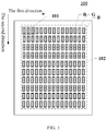
- FIG. 1 illustrates a top view of an exemplary array substrate consistent with disclosed embodiments
- FIG. 2 illustrates a schematic structural diagram of an exemplary pixel region of an exemplary array substrate consistent with disclosed embodiments
- FIG. 3 illustrates a schematic simulation diagram of an exemplary adjustment-subpixel region of an exemplary array substrate consistent with disclosed embodiments
- FIG. 4 illustrates a schematic simulation diagram of an exemplary non-adjustment-subpixel region of an exemplary array substrate consistent with disclosed embodiments
- FIG. 5 illustrates a schematic structural diagram of an exemplary adjustment electrode consistent with disclosed embodiments
- FIG. 6 illustrates a schematic structural diagram of a normal non-adjustment electrode
- FIG. 7 illustrates a schematic structural diagram of an exemplary first electrode consistent with disclosed embodiments
- FIG. 8 illustrates another schematic structural diagram of an exemplary first electrode consistent with disclosed embodiments
- FIG. 9 illustrates another schematic structural diagram of an exemplary first electrode consistent with disclosed embodiments.
- FIG. 10 illustrates a schematic structural diagram of an exemplary pixel region of an exemplary array substrate consistent with disclosed embodiments
- FIG. 11 illustrates a schematic structural diagram of an exemplary non-adjustment electrode of an exemplary array substrate consistent with disclosed embodiments
- FIG. 12 illustrates another schematic structural diagram of an exemplary non-adjustment electrode of an exemplary array substrate consistent with disclosed embodiments
- FIG. 13 illustrates a schematic structural diagram of an exemplary pixel region consistent with disclosed embodiments
- FIG. 14 illustrates another schematic structural diagram of an exemplary pixel region consistent with disclosed embodiments
- FIG. 15 illustrates another schematic structural diagram of an exemplary pixel region consistent with disclosed embodiments
- FIG. 16 illustrates another schematic structural diagram of an exemplary pixel region consistent with disclosed embodiments
- FIG. 17 illustrates another schematic structural diagram of an exemplary pixel region consistent with disclosed embodiments
- FIG. 18 illustrates another schematic structural diagram of an exemplary pixel region consistent with disclosed embodiments
- FIG. 19 illustrates another schematic structural diagram of an exemplary pixel region consistent with disclosed embodiments
- FIG. 20 illustrates a cross-sectional view of an exemplary array substrate consistent with disclosed embodiments
- FIG. 21 illustrates a schematic structural diagram of an exemplary display panel consistent with disclosed embodiments
- FIG. 22 illustrates a top view of an exemplary color-film substrate consistent with disclosed substrate.
- FIG. 23 illustrates a schematic structural diagram of an exemplary display device consistent with disclosed embodiments.
- first device is described as being coupled to a second device, it represents that the first device can be directly electrically coupled to the second device, or indirectly electrically coupled to the second device through another device or a coupling manner.
- first device can be directly electrically coupled to the second device, or indirectly electrically coupled to the second device through another device or a coupling manner.
- the adjustment of the displayed picture color of a display panel is achieved by reducing the voltage applied at a pixel unit of a certain color. As the voltage decreases, the electric-field-induced torque exerted on the liquid crystal molecules reduces, and their response time increases. This leads to an inconsistent response time for the subpixel units with different colors. After the response time exceeds the picture switching time, LCD motion artifacts (e.g., motion blur) can be observed upon a page being dragged or moved. Due to the inconsistent response time for different colors, a character discoloration trail is prone to occur. And the larger the discrepancy in the response time of the subpixel units of different colors is, the more evident the discoloration trail will be, thereby significantly degrading user experience.
- LCD motion artifacts e.g., motion blur
- an opening may be configured at the end points, away from first straight portions, between the at least two adjacent second portions of second portions corresponding to adjustment electrodes.
- an angle ⁇ 2 between an extending direction of the second straight portion and a second direction may be set to be greater than an angle ⁇ 1, between an extending direction of the first straight portions and the second direction.
- FIG. 1 illustrates a top view of an exemplary array substrate consistent with disclosed embodiments.
- FIG. 2 illustrates a schematic structural diagram of an exemplary pixel region of an exemplary array substrate consistent with disclosed embodiments.
- the array substrate 100 consistent with the present disclosure includes a plurality of pixel regions 101 , arranged in an array along a first direction and a second direction. Each of the pixel regions includes at least three subpixel regions 102 . Each of the subpixel regions 102 is configured with a first electrode 41 . The first direction intersects with the second direction.
- Each of the first electrodes 41 includes at least two first straight portions 51 parallel to each other and a second straight portion 52 connected to each of the first straight portions 51 .
- the second straight portions 52 of each of the first electrode 41 is parallel to each other and is disposed at a first end of each of the first straight portions 51 , respectively.
- a second end of each of the first straight portions 51 is connected with a first connecting portion 61 .
- At least one subpixel region 102 is an adjustment subpixel region 103 .
- the first electrode 41 corresponding to the adjustment subpixel region 103 is an adjustment electrode 42 .
- An opening 50 is configured between at least two adjacent second straight portions 52 of the second straight portions corresponding to each of the adjustment electrodes 42 at an end away from the first straight portions 51 .
- a plurality of pixel regions 101 are arranged in an array along the first direction and the second direction on the array substrate 100 .
- Each pixel region 101 includes three subpixel regions 102 .
- the first direction and the second direction may be perpendicular to each other.
- the first direction and the second direction may also be intersected in other manners according to specific applications, which are not limited herein.
- each subpixel region 102 is configured with the first electrode 41 .
- Each first electrode 41 includes two first straight portions 51 parallel to each other.
- a first end of the first straight portion 51 includes two second straight portions 52 parallel to each other, and the second straight portions 52 are connected to the first straight portions 51 in one-to-one correspondence.
- a second end of the first straight portions 51 is connected with a first connecting portion 61 .
- the first straight portion 51 deviates from the second direction with a certain angle, and the angle, between the extending direction of the first straight portion 51 and the second direction, is ⁇ 1.
- one subpixel region 102 serves as the adjustment-subpixel region 103 , and an opening 50 is configured at the end points, away from the first straight portions 51 , between the two second straight portions 52 corresponding to the adjustment electrode 42 of the subpixel region 103 . That is, at the end points (away from the first straight portions 51 ) of the second straight portions 52 , no electrode structure is configured.
- the electric-field directions, generated between the mutually parallel second straight portions 52 and a common electrode, can be consistent, which allows the liquid crystal molecules to have a consistent rotation direction at the end points (away from the first straight portions 51 ) of the second straight portions 52 .
- this opening is favorable to improve the transmittance of the adjustment-subpixel region 103 .
- FIG. 3 illustrates a schematic simulation diagram of an exemplary adjustment-subpixel region of an exemplary array substrate consistent with disclosed embodiments
- FIG. 4 illustrates a schematic simulation diagram of an exemplary non-adjustment-subpixel region of an exemplary array substrate consistent with disclosed embodiments.
- FIG. 3 there is no shadow present on the top of the adjustment-subpixel region 103 , which has a high transmittance.
- FIG. 4 there is a shadow present on the top of the non-adjustment-subpixel region 104 , which has a low transmittance.
- the rotation direction of the liquid crystal molecules corresponding to the top of the non-adjustment-subpixel region 104 is different from the rotation direction of the liquid crystal molecules corresponding to other regions, which leads to a reduced transmittance, and results in the shadow appearing on the top of the non-adjustment-subpixel region 104 (as shown in FIG. 4 ).
- the adjustment subpixel region 103 consistent with the present disclosure is illuminated, compared to non-adjustment-subpixel regions 104 , more lights from the opening 50 can pass through the adjustment-sub pixel region 103 , improving the transmittance of the adjustment-subpixel region 103 . Therefore, as required when displaying certain pictures, upon lowering the voltage of the adjustment-subpixel region 103 , the electric-field-induced torque exerted on the liquid crystal molecules 30 is reduced. Although the voltage decreases, because of the opening 50 between the second straight portions 52 of the adjustment subpixel region 103 , which helps to compensate for the reduced transmittance caused by the voltage decrease, the impact of decreasing the voltage on the overall transmittance of the array substrate 100 can be prevented.
- the angle ⁇ 2, between the extending direction of the second straight portion 52 of the adjustment electrode 42 and the second direction may be greater than the angle ⁇ 1, between the extending direct on of the first straight portion 51 and the second direction.
- the generated electric-field intensity corresponding to the adjustment-subpixel region 103 can be increased, thus increasing the voltage that can cause the rotation of the liquid crystal molecules.
- the residual torque can cause the rotation of the liquid crystal molecules.
- the angle ⁇ 1 between the extending direction of the first straight portion 51 and the second direction may be set as 6° ⁇ 1 ⁇ 14°
- the angle ⁇ 2 between the extending direction of the second straight portion 52 and the second direction may be set as ⁇ 2>14°.
- the response time of the subpixel region 102 corresponding to the adjustment-electrode 42 can be reduced to some extent, and the discrepancy in the response time among the subpixel regions 102 of different colors can be reduced, thereby effectively preventing motion blur and discoloration when dragging or moving a page and a character, and significantly improving the display quality of the array substrate 100 and enhancing the user experience.
- Table 1 and Table 2 represent comparison data of the simulated response time and the simulated transmittance, respectively, between the non-adjustment electrode 43 and the adjustment, electrode 42 .
- the angle ⁇ 2 between the extending direction of the second straight portion 52 and the second direction is set to different values.
- the non-adjustment electrode 43 there is an enclosure at the end points (away from the first straight portions 51 ) of the second straight portions 52 , and the second straight portions 52 are aligned with the first straight portions 51 .
- FIG. 5 illustrates a schematic structural diagram of an exemplary adjustment electrode consistent with disclosed embodiments
- FIG. 6 illustrates a schematic structural diagram of a normal non-adjustment electrode.
- the response time of the seal pixel region 102 having the adjustment electrode 42 can be evidently expedited, and the discrepancy in the response time among the subpixel regions 102 of different colors can be significantly lowered, which also can significantly improve the overall transmittance of the array substrate 100 , can effectively prevent motion blur and discoloration when dragging or moving a page or a character on the array substrate, and can considerably enhance the user experience.
- the length D of the second straight portion 52 of the adjustment electrode 42 may be set as 3 ⁇ m ⁇ D ⁇ 8 ⁇ m. Since during displaying by the array substrate, in the adjustment electrode 42 , the length of the second straight portion 52 and the angle of deviation from the second direction would affect the transmittance of the array substrate and the response time of the subpixel regions, under the precondition of ⁇ 2> ⁇ 1 (i.e., the angle between the extending direction of the second straight portion 52 and the second direction is larger than the angle, between the extending direction of the first straight portion 51 and the second direction), setting the length D of the second straight portion 52 of the adjustment electrode 42 as 3 ⁇ m ⁇ D ⁇ 8 ⁇ m can facilitate to improve the overall transmittance of the array substrate 100 .
- the opening 50 may be configured at the end points (away from the first straight portions 51 ) between any two adjacent second straight portions 52 .
- the first electrode 41 includes two first straight portions 51 parallel to each other, and correspondingly includes two second straight portions 52 connected to the two first straight portions 51 , respectively.
- the first electrode 41 may also include a plurality of the first straight portions 51 and a plurality of the second straight to portions 52 .
- the number of the first straight portions 51 and the number of the second straight portions 52 included in the first electrode 41 are not limited herein.
- FIG. 7 illustrates a schematic structural diagram of an exemplary first electrode consistent with disclosed embodiments
- FIG. 8 illustrates another schematic structural diagram of an exemplary first electrode consistent with disclosed embodiments
- FIG. 9 illustrates another schematic structural diagram of an exemplary first electrode consistent with disclosed embodiments.
- each of the first electrodes 41 includes three first straight portions 51 parallel to each other, and three second straight portions 52 parallel to each other.
- the end points (away from the first straight portions 51 ) of the adjacent second straight portions 52 are connected with the second connecting portion 62 .
- an opening 50 is configured at the end points (away from the first straight portions 51 ) of a pair of the adjacent second straight portions 52 .
- the opening 50 configured as shown in FIG. 8 ran improve the overall transmittance of the array substrate 100 .
- FIG. 8 ran improve the overall transmittance of the array substrate 100 .
- an opening 50 is configured, respectively, at the end points of each pair of the adjacent second straight portions 52 , which can be more favorable to improve the overall transmittance of the array substrate IOU than the structure having each of the second straight portions 52 enclosed. It should be noted that in the adjustment electrode 42 , as long as any two adjacent second straight portions 52 are configured with the opening 50 at the end points away from the first straight portions 51 , the overall transmittance of the array substrate 100 can be improved.
- the number and the position, of the opening 50 are not limited herein.
- FIG. 10 illustrates a schematic structural diagram of an exemplary to pixel region of an exemplary array substrate consistent with disclosed embodiments
- FIG. 11 illustrates a schematic structural diagram of an exemplary non-adjustment electrode of an exemplary array substrate consistent with disclosed embodiments.
- at least one subpixel region 102 may serve as the non-adjustment-subpixel region 104 .
- the first electrode corresponding to the non-adjustment-subpixel region 104 may serve as the non-adjustment electrode 43 , and the angle, between the extending direction of the second straight portion 52 of the non-adjustment electrode 43 and the second direction, is ⁇ 3 , and ⁇ 3 ⁇ 2.
- one pixel region 101 shown in FIG. 10 includes three subpixel regions 102 .
- One of the three subpixel regions 102 may serve as the non-adjustment-subpixel region 104
- the other two subpixel regions 102 may serve as the adjustment-subpixel regions 103 .
- one pixel region 101 may include two non-adjustment-subpixel regions 104 and one adjustment-subpixel region 103 , which is not limited herein.
- the angle, deviated from the extending direction of the second straight portion 52 of the non-adjustment electrode 43 to the second direction, is ⁇ 3.
- the angel ⁇ 2 between the extending direction of the second straight portion 52 of the adjustment electrode 42 and the second direction needs to be larger than the angle ⁇ 3, between the extending direction of the second straight portion 52 of the non-adjustment electrode 43 and the second direction.
- FIG. 12 illustrates another schematic structural diagram of an exemplary non-adjustment electrode of an exemplary array substrate consistent with disclosed embodiments.
- each of the second straight portions 52 of the non-adjustment electrode 43 may be connected with the second connecting portion 62 .
- the electrode corresponding to the non-adjustment-subpixel region 104 may serve as the non-adjustment electrode 43 .
- the end points (away from the first straight portions 51 ) of the second straight portions 52 of the non-adjustment electrode 43 are enclosed, that is, the second straight portions 52 are connected with the second connecting portion 62 .
- FIG. 13 illustrates a schematic structural diagram of an exemplary pixel region consistent with disclosed embodiments.
- the pixel region 101 includes a red subpixel region R, a blue subpixel region B, and a green subpixel region G.
- red, blue, and green colors as the three primary colors, a variety of colors can be formed, to meet the display requirements of colors during displaying by the array substrate 100 .
- FIG. 14 illustrates another schematic structural diagram of an exemplary pixel region consistent with disclosed embodiments.
- the pixel region 101 includes a red subpixel region R, a blue subpixel region B, a green subpixel region G, and a fourth-color subpixel region X.
- the fourth-color subpixel region X may be introduced to improve the display effect of the array substrate 100 .
- FIG. 15 illustrates another schematic structural diagram of an exemplary pixel region consistent with disclosed embodiments.
- the fourth-color subpixel region 102 shown in FIG. 15 is a white subpixel region W.
- introduction of the white subpixel region W can facilitate to improve the overall brightness of the picture displayed by the array substrate 100 .
- subpixel regions having other colors may also be used as the fourth-color subpixel region 102 , which is not limited herein.
- the white subpixel region W may be preferably selected as the adjustment-subpixel region.
- the white subpixel region W By controlling the voltage of the white subpixel region W, adjusting the brightness of the picture displayed by the array substrate 100 can be achieved.
- the pixel, region 101 may include at least one adjustment-subpixel region 103 and at least one non-adjustment-subpixel region 104 . That is, in each pixel region 101 on the array substrate 100 , both the adjustment-subpixel region 103 and the non-adjustment-subpixel region 104 may be included.
- the adjustment-subpixel region 103 may employ the adjustment electrode 42
- the non-adjustment-subpixel region 104 may employ the non-adjustment electrode 43 .
- the design of the adjustment electrode 42 consistent with the present disclosure can facilitate to expedite the response time of the subpixel region 103 , and can lower the discrepancy in the response time between the adjustment subpixel region 103 and the non-adjustment-subpixel region 104 . Meanwhile, the design of the opening 50 in the adjustment electrode 42 can further compensate the transmittance of the adjustment subpixel region 103 , thus not causing an impact on the overall transmittance of the array substrate 100 .
- the blue subpixel region B may serve as the adjustment-subpixel region 103
- the red subpixel region R and the green subpixel region G may serve as the non-adjustment-subpixel regions 104 .
- the blue subpixel region B may serve as the adjustment-subpixel region 103
- the electrode corresponding to the blue subpixel region B may serve as the adjustment electrode 43 .
- the transmittance corresponding to the blue subpixel region B would decrease.
- the top of the adjustment electrode 42 corresponding to the blue subpixel region B may be contrived in the form of a non-enclosed end, that is, an opening 50 may be contrived at the end points (away from the first straight portions 51 ) of the second straight portions 52 of the adjustment electrode 42 , thereby improving the transmittance of the blue subpixel region B, compensating for the reduced transmittance with decrease in the voltage, and preventing the impact of reducing voltage on the overall transmittance of the array substrate 100 .
- the angle ⁇ 2 between the extending direction of the second straight portion 52 and the second direction is greater than the angle ⁇ 1, between the extending direction of the first straight portion 51 and the second direction
- the response time of the blue subpixel region B can be expedited, the discrepancy in the response time, among the blue subpixel region B, the green subpixel region G and the red-green subpixel region 102 , can be reduced, thus improving the artifacts of motion blur and discoloration in the existing technologies and enhancing the user experience.
- FIG. 16 illustrates another schematic structural diagram of an exemplary pixel region consistent with disclosed embodiments.
- the blue subpixel region B and the green subpixel region G may serve as the adjustment-subpixel regions 103
- the red subpixel region R may serve as the non-adjustment-subpixel region 104 .
- the brightness of the blue subpixel region B and the green subpixel region G can be reduced, causing the picture displayed by the array substrate 100 to be orange-yellow.
- the transmittances corresponding to the blue subpixel region B and the green subpixel region G would be lowered.
- the tops of the adjustment electrodes 42 corresponding to the blue subpixel region B and the green subpixel region G may be contrived in the form of non-enclosed ends, that is, openings 50 may be contrived at the end points (away from the first straight portions 51 ) of the second straight portions 53 of the adjustment electrode 42 , thereby improving the transmittances of the blue subpixel region B and the green subpixel region compensating for the reduced transmittance with decrease in the voltage, and preventing the impact of reducing the voltage on the overall transmittance of the array substrate 100 .
- the angle ⁇ 2 between the extending direction of the second straight portion 52 and the second direction is greater than the angle ⁇ 1, between the extending direction of the first straight portion 51 and the second direction
- the response time of the blue subpixel region B can be expedited, the discrepancy in the response time, among the blue subpixel region B, the green subpixel region G and the red-green subpixel region 102 , can be reduced, thus improving the artifacts of motion blur and discoloration in the existing technologies and enhancing the user experience.
- FIG. 17 illustrates another schematic structural diagram of an exemplary pixel region consistent with disclosed embodiments.
- the red subpixel region R and the green subpixel region G may serve as the adjustment-subpixel regions 103
- the blue subpixel region B may serve as the non-adjustment-subpixel region 104 .
- the brightness of the red subpixel region R and the green subpixel region G can be reduced, causing the picture displayed by the array substrate 100 to be bluish purple.
- the transmittances corresponding to the red subpixel region R and the green subpixel region G would be lowered.
- the tops of the adjustment electrodes 42 corresponding to the red subpixel region R and the green subpixel region G may be contrived in the form non-enclosed ends, that is, openings 50 may be contrived at the end points (away from the first straight portions 51 ) of the second straight portions 52 of the adjustment electrodes 42 , thereby improving the transmittances of the red subpixel region R and the green subpixel region G, compensating for the reduced transmittance with decrease in the voltage, and preventing the impact of reducing the voltage on the overall transmittance of the array substrate 100 .
- the angle ⁇ 2 between the extending direction of the second straight portion 52 and the second direction is greater than the angle ⁇ 1, between the extending direction of the first straight portion 51 and the second direction
- the response time of the red subpixel region R and the green subpixel region G can be expedited, the discrepancy in the response time, among the red subpixel region R, the green subpixel region G and the blue-green subpixel region 102 , can be reduced, thus improving the artifacts of motion blur and discoloration in the existing technologies and enhancing the user experience.
- the embodiments shown in FIGS. 14-17 only illustrate three different examples, where the pixel region 101 includes the three red, green, and blue subpixel regions 102 .
- a user can contrive the subpixel regions specifically corresponding to the adjustment-subpixel region 103 and the non-adjustment-subpixel region 104 , which is not limited herein.
- the pixel region 101 includes the four-color red, green, blue and white subpixel regions, according to the requirements, the user can also select which subpixel region to serve as the adjustment-subpixel region 103 or the non-adjustment-subpixel region 104 , which is not limited herein either.
- FIG. 18 illustrates another schematic structural diagram of an exemplary pixel region consistent with disclosed embodiments
- FIG. 19 illustrates another schematic structural diagram of an exemplary pixel region consistent with disclosed embodiments.
- each of the subpixel regions 102 may serve as the adjustment subpixel region 103 .
- the first electrode 41 corresponding to each of the subpixel regions 102 may serve as the adjustment electrode 42 .
- An opening 50 may be configured at the end points (away from the first straight portions 51 ) of the second straight portions 52 in each of the adjustment electrodes 42 .
- This design can improve the transmittance for each of the subpixel regions 102 , thus improving the overall transmittance, and in turn enhancing the display effect of the array substrate 100 .
- FIG. 20 illustrates a cross-sectional view of an exemplary array substrate consistent with disclosed embodiments.
- the first electrode 41 may serve as a pixel electrode
- the array substrate 100 may further include a common electrode 48 .
- the common electrode 48 and the pixel electrode 41 may be insulated by an insulating layer 80 .
- the pixel electrode 41 and the common electrode 48 may be arranged to be opposite to each other.
- the common electrode 48 may receive a first voltage and the pixel electrode may receive a second voltage. The voltage difference between the first voltage and the second voltage may serve as a driving voltage for driving the liquid crystal molecules to rotate. Referring to FIG.
- the array substrate 100 consistent with the present disclosure may also include a first substrate 11 , a buffer layer 12 , and an array layer of thin-film transistors 40 .
- the array layer of thin-film transistors 40 may include a semiconductor active layer 25 on the buffer layer 12 .
- the semiconductor active layer 25 may include a source region and a drain region formed by doping N-type or P-type impurity ions. The region between the source region and the drain region is a channel region without being doped with impurity ions.
- the semiconductor active layer 25 may be formed by crystallizing amorphous silicon into polysilicon.
- RTA rapid thermal annealing
- SPC solid phase crystallization
- ELA excimer laser annealing
- MILC metal-induced lateral crystallization
- SLS continuous lateral solidification
- a gate insulating layer 26 may be disposed on the semiconductor active, layer 25 , and the gate insulating layer 26 may include one or more of inorganic layers, such as silicon oxide, silicon nitride, metal oxide, etc.
- a first metal layer 21 may be disposed in a certain region on the gate insulating layer 26 , and may serve as a gate electrode of the thin-film transistor.
- the gate electrode may include one or more layers of metal elements, such as gold (Au), silver (Ag), copper (Cu), nickel (Ni), platinum (Pt), palladium (Pd), aluminum (Al), molybdenum (Mo), chromium (Cr), etc.
- the gate electrode may include one or more layers of metal alloys, such as aluminum-neodymium (Al—Nd) molybdenum-tungsten (Mo—W) alloy, etc.
- An inter-insulating layer 24 may be disposed on the first metal layer 21 , and may be formed by an insulating inorganic layer such as silicon oxide, silicon nitride, etc. or formed by an insulating organic layer.
- a second metal layer 22 may be disposed on the inter-insulating layer 24 , and may serve as a source electrode 27 and a drain electrode 28 of the thin-film transistor.
- the source electrode 27 and the drain electrode 28 may be electrically connected through a contact hole 29 to the source region and the drain region of the semiconductor active layer 25 , respectively.
- the contact hole 29 may be formed by selectively removing the gate insulating layer 26 and the inter-insulating layer 24 .
- a passivation layer 23 may be disposed on the second metal layer 22 , and may be framed by the inorganic layer such as silicon oxide, silicon nitride, etc., or formed by the organic layer.
- the common electrode 48 , the insulating layer 80 , and the pixel electrode 41 may be configured on the side (away from the second metal layer 22 ) of the passivation layer 23 .
- the embodiments shown in FIG. 20 are illustrated by taking the thin-film transistor having a top-gate structure as an example.
- the thin-film transistor may also have a bottom-gate structure.
- FIG. 21 illustrates a schematic structural diagram of an exemplary display panel consistent with disclosed embodiments.
- the display panel 300 may include the array substrate 100 consistent with the present disclosure and a color-film substrate 200 opposite to the array substrate 100 .
- the liquid crystal molecules 30 may be filled between the array substrate 100 and the color-film substrate 200 .
- the liquid crystal molecules 30 are rotated, which allows the display panel 300 to display normally.
- the embodiments of the display panel 300 consistent with the present disclosure can refer to the foregoing embodiments of the array substrate 100 , which are not repeated herein.
- FIG. 22 illustrates a top view of an exemplary color-film substrate consistent with disclosed substrate.
- the color-film substrate 200 may be configured with a plurality of red resistances r, blue resistances b and green resistances g.
- the array substrate 100 may be configured with the plurality of red subpixel regions R, blue subpixel regions B and green subpixel regions G.
- the red resistances r, the blue resistances b and the green resistances g may correspond to the red subpixel regions R, the blue subpixel regions B and the green subpixel regions G, respectively.
- the red resistances r, the blue resistances b and the green resistances g may cooperate with the red subpixel regions R, the blue subpixel regions B and the green subpixel regions G, respectively, to achieve the display for different pictures and colors on the display panel 300 .
- FIG. 23 illustrates a schematic structural diagram of an exemplary display device consistent with disclosed embodiments.
- the display device 400 may include the display panel 300 consistent with the present disclosure.
- the display device 400 consistent with the present disclosure may be any products or components having a real function, such as a mobile phone, a tablet computer, a television, a monitor, a notebook computer, a digital photo frame, a navigator, etc.
- the embodiments of the display device 400 consistent with the present disclosure can refer to the foregoing embodiments of the display panel 300 , which are not repeated herein.
- the beneficial effects of the present disclosure includes: of the array substrate, the display panel and the display device consistent with the present disclosure, in the at least three subpixel regions included by each pixel region, at least one subpixel region may serve as the adjustment-subpixel region; an opening may be configured at the end points, away from the first straight portions, between the at least two adjacent second straight portions of the second straight portions corresponding to the adjustment electrode; and the angle ⁇ 2, between the extending direction of the second straight portion of the adjustment electrode and the second direction, may be set to be greater than the angle ⁇ 1, between the extending direction of the first, straight portion and the second direction.
- Such design can effectively prevent the decrease of transmittance, and meanwhile can speed up the pixel response time, lower the discrepancy in the response time among each subpixel, and improve the artifacts of motion blur and discoloration in the existing technologies.
Landscapes
- Physics & Mathematics (AREA)
- Nonlinear Science (AREA)
- Mathematical Physics (AREA)
- Chemical & Material Sciences (AREA)
- Crystallography & Structural Chemistry (AREA)
- General Physics & Mathematics (AREA)
- Optics & Photonics (AREA)
- Geometry (AREA)
- Engineering & Computer Science (AREA)
- Microelectronics & Electronic Packaging (AREA)
- Liquid Crystal (AREA)
- Spectroscopy & Molecular Physics (AREA)
Abstract
Description
| TABLE 1 |
| Comparison of simulated response time |
| GTG MAX | Ton + Toff | ||||
| Simulated results | θ2 | unit:ms | unit:ms | ||
| Non-adjustment | θ2 = 10° | 40.3 | 29.5 | ||
| electrode | |||||
| Adjustment | θ2 = 14° | 39.4 | 28.6 | ||
| electrode | θ2 = 17° | 38.9 | 28.5 | ||
| θ2 = 20° | 38.6 | 28.5 | |||
| TABLE 2 |
| Comparison of simulated transmittance |
| Increasing rate of | |||
| Simulated results | θ2 | TR | TR |
| Non-adjustment electrode | θ2 = 10° | 3.34% | — |
| Adjustment electrode | θ2 = 14° | 3.26% | −2.4% |
| θ2 = 17° | 3.25% | −2.7% | |
| θ2 = 20° | 3.37% | 0.9% | |
| θ2 = 25° | 3.35% | 0.3% | |
| θ2 = 30° | 1.34% | 0 | |
Claims (19)
Applications Claiming Priority (2)
| Application Number | Priority Date | Filing Date | Title |
|---|---|---|---|
| CN201810098638.1 | 2018-01-31 | ||
| CN201810098638.1A CN108363245B (en) | 2018-01-31 | 2018-01-31 | Array substrate, display panel and display device |
Publications (2)
| Publication Number | Publication Date |
|---|---|
| US20190235324A1 US20190235324A1 (en) | 2019-08-01 |
| US11061284B2 true US11061284B2 (en) | 2021-07-13 |
Family
ID=63007663
Family Applications (1)
| Application Number | Title | Priority Date | Filing Date |
|---|---|---|---|
| US15/993,154 Active 2039-05-22 US11061284B2 (en) | 2018-01-31 | 2018-05-30 | Array substrate comprising electrode having parallel straight portions, display panel, and display device |
Country Status (2)
| Country | Link |
|---|---|
| US (1) | US11061284B2 (en) |
| CN (1) | CN108363245B (en) |
Families Citing this family (1)
| Publication number | Priority date | Publication date | Assignee | Title |
|---|---|---|---|---|
| CN113050319B (en) * | 2021-04-02 | 2022-07-19 | 厦门天马微电子有限公司 | Display panel and display device |
Citations (9)
| Publication number | Priority date | Publication date | Assignee | Title |
|---|---|---|---|---|
| US20100128208A1 (en) * | 2008-11-27 | 2010-05-27 | Epson Imaging Devices Corporation | Liquid crystal display device |
| US20140125904A1 (en) * | 2012-11-06 | 2014-05-08 | Samsung Display Co., Ltd. | Liquid crystal display |
| CN103885260A (en) | 2014-02-26 | 2014-06-25 | 友达光电股份有限公司 | Display panel |
| US20140240629A1 (en) * | 2013-02-26 | 2014-08-28 | Xiamen Tianma Micro-Electronics Co., Ltd. | Pixel unit and array substrate of liquid crystal display device with a fringe field switching mode |
| CN104570514A (en) | 2014-12-30 | 2015-04-29 | 厦门天马微电子有限公司 | Electrode structure and liquid crystal display panel |
| US20160291423A1 (en) * | 2015-03-31 | 2016-10-06 | Au Optronics Corporation | Pixel structure and liquid crystal display including the same |
| CN106324936A (en) | 2016-11-21 | 2017-01-11 | 厦门天马微电子有限公司 | Pixel array substrate, liquid crystal display panel and liquid crystal display device |
| CN106773371A (en) | 2016-12-29 | 2017-05-31 | 武汉华星光电技术有限公司 | A kind of array base palte and display panel |
| CN107422549A (en) | 2017-09-29 | 2017-12-01 | 厦门天马微电子有限公司 | Display panel and display device |
Family Cites Families (8)
| Publication number | Priority date | Publication date | Assignee | Title |
|---|---|---|---|---|
| JP3194127B2 (en) * | 1996-04-16 | 2001-07-30 | 大林精工株式会社 | Liquid crystal display |
| JP4201574B2 (en) * | 2002-10-31 | 2008-12-24 | 奇美電子股▲ふん▼有限公司 | Image display device |
| KR100517345B1 (en) * | 2003-05-31 | 2005-09-28 | 삼성전자주식회사 | Liquid Crystal Display |
| KR20120017351A (en) * | 2010-08-18 | 2012-02-28 | 삼성전자주식회사 | Liquid crystal display |
| CN102998857B (en) * | 2012-11-20 | 2015-07-15 | 京东方科技集团股份有限公司 | Slit electrode, array substrate and display device |
| CN104503149B (en) * | 2014-12-30 | 2017-09-19 | 南京中电熊猫液晶显示科技有限公司 | Liquid crystal display panel and photo-alignment method thereof |
| CN105093723A (en) * | 2015-09-08 | 2015-11-25 | 深圳市华星光电技术有限公司 | Liquid crystal display panel capable of improving color error |
| CN107450240B (en) * | 2017-09-19 | 2020-06-16 | 惠科股份有限公司 | Array substrate and display panel thereof |
-
2018
- 2018-01-31 CN CN201810098638.1A patent/CN108363245B/en active Active
- 2018-05-30 US US15/993,154 patent/US11061284B2/en active Active
Patent Citations (11)
| Publication number | Priority date | Publication date | Assignee | Title |
|---|---|---|---|---|
| US20100128208A1 (en) * | 2008-11-27 | 2010-05-27 | Epson Imaging Devices Corporation | Liquid crystal display device |
| US20140125904A1 (en) * | 2012-11-06 | 2014-05-08 | Samsung Display Co., Ltd. | Liquid crystal display |
| US20140240629A1 (en) * | 2013-02-26 | 2014-08-28 | Xiamen Tianma Micro-Electronics Co., Ltd. | Pixel unit and array substrate of liquid crystal display device with a fringe field switching mode |
| CN103885260A (en) | 2014-02-26 | 2014-06-25 | 友达光电股份有限公司 | Display panel |
| CN103885260B (en) | 2014-02-26 | 2017-01-18 | 友达光电股份有限公司 | Display panel |
| CN104570514A (en) | 2014-12-30 | 2015-04-29 | 厦门天马微电子有限公司 | Electrode structure and liquid crystal display panel |
| US20160291423A1 (en) * | 2015-03-31 | 2016-10-06 | Au Optronics Corporation | Pixel structure and liquid crystal display including the same |
| CN106324936A (en) | 2016-11-21 | 2017-01-11 | 厦门天马微电子有限公司 | Pixel array substrate, liquid crystal display panel and liquid crystal display device |
| CN106773371A (en) | 2016-12-29 | 2017-05-31 | 武汉华星光电技术有限公司 | A kind of array base palte and display panel |
| US20180336829A1 (en) * | 2016-12-29 | 2018-11-22 | Wuhan China Star Optoelectronics Technology Co., Ltd. | Array substrate and display panel |
| CN107422549A (en) | 2017-09-29 | 2017-12-01 | 厦门天马微电子有限公司 | Display panel and display device |
Also Published As
| Publication number | Publication date |
|---|---|
| CN108363245A (en) | 2018-08-03 |
| US20190235324A1 (en) | 2019-08-01 |
| CN108363245B (en) | 2021-02-09 |
Similar Documents
| Publication | Publication Date | Title |
|---|---|---|
| US9991296B2 (en) | Liquid crystal display with pixel transistors having different channel widths | |
| US11054706B2 (en) | Display device | |
| US10197870B2 (en) | Array substrate and display device | |
| WO2020199515A1 (en) | Display device | |
| US11422419B2 (en) | Display device | |
| US20200117062A1 (en) | Display device | |
| CN107976836B (en) | Display panel and display device | |
| KR102567648B1 (en) | Liquid crystal display device | |
| US10775676B2 (en) | Display device | |
| US20100177256A1 (en) | Thin film transistor substrate and liquid crystal display having the same | |
| US11137652B2 (en) | Array substrate and fabrication method thereof, and display device | |
| US11061284B2 (en) | Array substrate comprising electrode having parallel straight portions, display panel, and display device | |
| KR102068962B1 (en) | Array substrate for liquid crystal display device | |
| CN107422549B (en) | Display panel and display device | |
| KR102129500B1 (en) | Liquid crystal display panel | |
| CN104122721B (en) | Pixel structure | |
| CN105842945A (en) | Liquid crystal display | |
| KR20160132245A (en) | Display device | |
| CN108535926B (en) | Display panel and display device | |
| KR20160116189A (en) | Color filter panel and liquid crystal display including the same | |
| KR20160089938A (en) | Liquid crystal display | |
| US9658498B2 (en) | Liquid crystal display | |
| US20050146663A1 (en) | Vertically aligned mode liquid crystal display | |
| US11579502B2 (en) | Display device | |
| KR102081604B1 (en) | Array substrate for liquid crystal display device |
Legal Events
| Date | Code | Title | Description |
|---|---|---|---|
| AS | Assignment |
Owner name: XIAMEN TIANMA MICRO-ELECTRONICS CO., LTD., CHINA Free format text: ASSIGNMENT OF ASSIGNORS INTEREST;ASSIGNORS:LIANG, YUJIAO;FANG, LITING;LING, ANKAI;AND OTHERS;REEL/FRAME:045939/0059 Effective date: 20180525 |
|
| FEPP | Fee payment procedure |
Free format text: ENTITY STATUS SET TO UNDISCOUNTED (ORIGINAL EVENT CODE: BIG.); ENTITY STATUS OF PATENT OWNER: LARGE ENTITY |
|
| STPP | Information on status: patent application and granting procedure in general |
Free format text: NON FINAL ACTION MAILED |
|
| STPP | Information on status: patent application and granting procedure in general |
Free format text: RESPONSE TO NON-FINAL OFFICE ACTION ENTERED AND FORWARDED TO EXAMINER |
|
| STPP | Information on status: patent application and granting procedure in general |
Free format text: NOTICE OF ALLOWANCE MAILED -- APPLICATION RECEIVED IN OFFICE OF PUBLICATIONS |
|
| STPP | Information on status: patent application and granting procedure in general |
Free format text: AWAITING TC RESP., ISSUE FEE NOT PAID |
|
| STPP | Information on status: patent application and granting procedure in general |
Free format text: NOTICE OF ALLOWANCE MAILED -- APPLICATION RECEIVED IN OFFICE OF PUBLICATIONS |
|
| STPP | Information on status: patent application and granting procedure in general |
Free format text: PUBLICATIONS -- ISSUE FEE PAYMENT RECEIVED |
|
| STPP | Information on status: patent application and granting procedure in general |
Free format text: PUBLICATIONS -- ISSUE FEE PAYMENT VERIFIED |
|
| STCF | Information on status: patent grant |
Free format text: PATENTED CASE |
|
| MAFP | Maintenance fee payment |
Free format text: PAYMENT OF MAINTENANCE FEE, 4TH YEAR, LARGE ENTITY (ORIGINAL EVENT CODE: M1551); ENTITY STATUS OF PATENT OWNER: LARGE ENTITY Year of fee payment: 4 |