US11061125B2 - Symmetric receiver switch for bipolar pulser - Google Patents
Symmetric receiver switch for bipolar pulser Download PDFInfo
- Publication number
- US11061125B2 US11061125B2 US16/035,552 US201816035552A US11061125B2 US 11061125 B2 US11061125 B2 US 11061125B2 US 201816035552 A US201816035552 A US 201816035552A US 11061125 B2 US11061125 B2 US 11061125B2
- Authority
- US
- United States
- Prior art keywords
- transistor
- gate
- circuit
- voltage
- signal
- Prior art date
- Legal status (The legal status is an assumption and is not a legal conclusion. Google has not performed a legal analysis and makes no representation as to the accuracy of the status listed.)
- Active, expires
Links
- 238000002604 ultrasonography Methods 0.000 claims abstract description 60
- 238000000034 method Methods 0.000 claims description 25
- 230000008878 coupling Effects 0.000 claims description 10
- 238000010168 coupling process Methods 0.000 claims description 10
- 238000005859 coupling reaction Methods 0.000 claims description 10
- 230000011664 signaling Effects 0.000 claims 1
- 238000001514 detection method Methods 0.000 description 43
- 238000010586 diagram Methods 0.000 description 25
- 239000000758 substrate Substances 0.000 description 14
- 239000000523 sample Substances 0.000 description 9
- 239000004065 semiconductor Substances 0.000 description 9
- 230000005669 field effect Effects 0.000 description 8
- 239000003990 capacitor Substances 0.000 description 7
- 230000008901 benefit Effects 0.000 description 6
- 230000001419 dependent effect Effects 0.000 description 3
- 230000000694 effects Effects 0.000 description 3
- 230000001747 exhibiting effect Effects 0.000 description 3
- 230000004044 response Effects 0.000 description 3
- 238000012285 ultrasound imaging Methods 0.000 description 3
- XUIMIQQOPSSXEZ-UHFFFAOYSA-N Silicon Chemical compound [Si] XUIMIQQOPSSXEZ-UHFFFAOYSA-N 0.000 description 2
- 230000004075 alteration Effects 0.000 description 2
- 230000005540 biological transmission Effects 0.000 description 2
- 230000005684 electric field Effects 0.000 description 2
- 238000005516 engineering process Methods 0.000 description 2
- 238000003384 imaging method Methods 0.000 description 2
- 230000006872 improvement Effects 0.000 description 2
- 239000000463 material Substances 0.000 description 2
- 230000004048 modification Effects 0.000 description 2
- 238000012986 modification Methods 0.000 description 2
- 229910052710 silicon Inorganic materials 0.000 description 2
- 239000010703 silicon Substances 0.000 description 2
- 230000002459 sustained effect Effects 0.000 description 2
- 230000009286 beneficial effect Effects 0.000 description 1
- 230000003247 decreasing effect Effects 0.000 description 1
- 230000002542 deteriorative effect Effects 0.000 description 1
- 230000001627 detrimental effect Effects 0.000 description 1
- 238000005457 optimization Methods 0.000 description 1
- 230000008569 process Effects 0.000 description 1
- 230000001902 propagating effect Effects 0.000 description 1
- 238000002560 therapeutic procedure Methods 0.000 description 1
Images


Classifications
-
- G—PHYSICS
- G01—MEASURING; TESTING
- G01S—RADIO DIRECTION-FINDING; RADIO NAVIGATION; DETERMINING DISTANCE OR VELOCITY BY USE OF RADIO WAVES; LOCATING OR PRESENCE-DETECTING BY USE OF THE REFLECTION OR RERADIATION OF RADIO WAVES; ANALOGOUS ARRANGEMENTS USING OTHER WAVES
- G01S7/00—Details of systems according to groups G01S13/00, G01S15/00, G01S17/00
- G01S7/52—Details of systems according to groups G01S13/00, G01S15/00, G01S17/00 of systems according to group G01S15/00
- G01S7/521—Constructional features
-
- G—PHYSICS
- G01—MEASURING; TESTING
- G01S—RADIO DIRECTION-FINDING; RADIO NAVIGATION; DETERMINING DISTANCE OR VELOCITY BY USE OF RADIO WAVES; LOCATING OR PRESENCE-DETECTING BY USE OF THE REFLECTION OR RERADIATION OF RADIO WAVES; ANALOGOUS ARRANGEMENTS USING OTHER WAVES
- G01S7/00—Details of systems according to groups G01S13/00, G01S15/00, G01S17/00
- G01S7/52—Details of systems according to groups G01S13/00, G01S15/00, G01S17/00 of systems according to group G01S15/00
- G01S7/52017—Details of systems according to groups G01S13/00, G01S15/00, G01S17/00 of systems according to group G01S15/00 particularly adapted to short-range imaging
- G01S7/52019—Details of transmitters
- G01S7/5202—Details of transmitters for pulse systems
-
- G—PHYSICS
- G01—MEASURING; TESTING
- G01S—RADIO DIRECTION-FINDING; RADIO NAVIGATION; DETERMINING DISTANCE OR VELOCITY BY USE OF RADIO WAVES; LOCATING OR PRESENCE-DETECTING BY USE OF THE REFLECTION OR RERADIATION OF RADIO WAVES; ANALOGOUS ARRANGEMENTS USING OTHER WAVES
- G01S15/00—Systems using the reflection or reradiation of acoustic waves, e.g. sonar systems
- G01S15/88—Sonar systems specially adapted for specific applications
- G01S15/89—Sonar systems specially adapted for specific applications for mapping or imaging
- G01S15/8906—Short-range imaging systems; Acoustic microscope systems using pulse-echo techniques
- G01S15/8909—Short-range imaging systems; Acoustic microscope systems using pulse-echo techniques using a static transducer configuration
- G01S15/8915—Short-range imaging systems; Acoustic microscope systems using pulse-echo techniques using a static transducer configuration using a transducer array
-
- G—PHYSICS
- G01—MEASURING; TESTING
- G01S—RADIO DIRECTION-FINDING; RADIO NAVIGATION; DETERMINING DISTANCE OR VELOCITY BY USE OF RADIO WAVES; LOCATING OR PRESENCE-DETECTING BY USE OF THE REFLECTION OR RERADIATION OF RADIO WAVES; ANALOGOUS ARRANGEMENTS USING OTHER WAVES
- G01S7/00—Details of systems according to groups G01S13/00, G01S15/00, G01S17/00
- G01S7/52—Details of systems according to groups G01S13/00, G01S15/00, G01S17/00 of systems according to group G01S15/00
- G01S7/52017—Details of systems according to groups G01S13/00, G01S15/00, G01S17/00 of systems according to group G01S15/00 particularly adapted to short-range imaging
- G01S7/52046—Techniques for image enhancement involving transmitter or receiver
- G01S7/52047—Techniques for image enhancement involving transmitter or receiver for elimination of side lobes or of grating lobes; for increasing resolving power
-
- G—PHYSICS
- G01—MEASURING; TESTING
- G01S—RADIO DIRECTION-FINDING; RADIO NAVIGATION; DETERMINING DISTANCE OR VELOCITY BY USE OF RADIO WAVES; LOCATING OR PRESENCE-DETECTING BY USE OF THE REFLECTION OR RERADIATION OF RADIO WAVES; ANALOGOUS ARRANGEMENTS USING OTHER WAVES
- G01S7/00—Details of systems according to groups G01S13/00, G01S15/00, G01S17/00
- G01S7/52—Details of systems according to groups G01S13/00, G01S15/00, G01S17/00 of systems according to group G01S15/00
- G01S7/52017—Details of systems according to groups G01S13/00, G01S15/00, G01S17/00 of systems according to group G01S15/00 particularly adapted to short-range imaging
- G01S7/5205—Means for monitoring or calibrating
-
- G—PHYSICS
- G01—MEASURING; TESTING
- G01S—RADIO DIRECTION-FINDING; RADIO NAVIGATION; DETERMINING DISTANCE OR VELOCITY BY USE OF RADIO WAVES; LOCATING OR PRESENCE-DETECTING BY USE OF THE REFLECTION OR RERADIATION OF RADIO WAVES; ANALOGOUS ARRANGEMENTS USING OTHER WAVES
- G01S7/00—Details of systems according to groups G01S13/00, G01S15/00, G01S17/00
- G01S7/52—Details of systems according to groups G01S13/00, G01S15/00, G01S17/00 of systems according to group G01S15/00
- G01S7/52017—Details of systems according to groups G01S13/00, G01S15/00, G01S17/00 of systems according to group G01S15/00 particularly adapted to short-range imaging
- G01S7/52079—Constructional features
- G01S7/5208—Constructional features with integration of processing functions inside probe or scanhead
-
- H—ELECTRICITY
- H03—ELECTRONIC CIRCUITRY
- H03K—PULSE TECHNIQUE
- H03K17/00—Electronic switching or gating, i.e. not by contact-making and –breaking
- H03K17/51—Electronic switching or gating, i.e. not by contact-making and –breaking characterised by the components used
- H03K17/56—Electronic switching or gating, i.e. not by contact-making and –breaking characterised by the components used by the use, as active elements, of semiconductor devices
- H03K17/687—Electronic switching or gating, i.e. not by contact-making and –breaking characterised by the components used by the use, as active elements, of semiconductor devices the devices being field-effect transistors
- H03K17/6871—Electronic switching or gating, i.e. not by contact-making and –breaking characterised by the components used by the use, as active elements, of semiconductor devices the devices being field-effect transistors the output circuit comprising more than one controlled field-effect transistor
- H03K17/6874—Electronic switching or gating, i.e. not by contact-making and –breaking characterised by the components used by the use, as active elements, of semiconductor devices the devices being field-effect transistors the output circuit comprising more than one controlled field-effect transistor in a symmetrical configuration
Definitions
- the present application relates to ultrasound devices for ultrasound imaging and high intensity focused ultrasound (HIFU).
- HIFU high intensity focused ultrasound
- Some conventional ultrasound devices include pulsing circuits configured to provide pulses to an ultrasonic transducer. Often the ultrasonic transducer operates in transmission and reception.
- aspects of the present application provide an ultrasound-on-a-chip device including integrated circuitry having a pulser with feedback. Symmetric receive switches are also provided in the ultrasound-on-a-chip device and coupled to an output of the ultrasonic transducers to facilitate the use of multi-level pulsers to drive the ultrasonic transducers.
- An aspect of the present application relates to an ultrasound device comprising a capacitive ultrasonic transducer, a bipolar pulser coupled to the capacitive ultrasonic transducer and configured to provide, from an output terminal, a bipolar input signal to the capacitive ultrasonic transducer, a receiving circuit configured to process an electrical signal output by the capacitive ultrasonic transducer, and a symmetric switch comprising a first transistor and a second transistor.
- the symmetric switch has an input terminal coupled between the output terminal of the bipolar pulser and the capacitive ultrasonic transducer and having an output terminal coupled to the receiving circuit.
- an ultrasound device comprising providing a bipolar pulser signal from a bipolar pulser to a first terminal of a capacitive ultrasonic transducer during a transmit mode of operation of the ultrasound device, operating a symmetric switch coupled between the first terminal of the capacitive ultrasonic transducer and a receiving circuit in an open state during the transmit mode of operation, and operating the symmetric switch in a closed state during a receive mode of operation of the ultrasound device.
- FIG. 1 is a block diagram illustrating an ultrasound device including a plurality of pulsing circuits and a plurality of receiver switches, according to a non-limiting embodiment of the present application.
- FIG. 2 is a block diagram illustrating a pulsing circuit coupled to a capacitive ultrasonic transducer, according to a non-limiting embodiment of the present application.
- FIG. 3 is a block diagram illustrating a pulsing circuit comprising a pulser and a feedback circuit, according to a non-limiting embodiment of the present application.
- FIG. 4 is a block diagram illustrating the acts of a method to operate a pulsing circuit coupled to a capacitive ultrasonic transducer, according to a non-limiting embodiment of the present application.
- FIG. 5A is a circuit diagram illustrating a resistive ladder configured to generate a plurality of threshold voltages, according to a non-limiting embodiment of the present application.
- FIG. 5B is a circuit diagram illustrating a dividing circuit configured to generate a detection signal, according to a non-limiting embodiment of the present application.
- FIG. 6A illustrates a timing diagram showing an example signal provided by the pulsing circuit to the capacitive ultrasonic transducer, according to a non-limiting embodiment of the present application.
- FIG. 6B illustrates a timing diagram showing an apodized signal provided by the pulsing circuit to the capacitive ultrasonic transducer, according to a non-limiting embodiment of the present application.
- FIG. 7 is a block diagram illustrating a plurality of pulsing circuits coupled to a plurality of capacitive ultrasonic transducers, according to a non-limiting embodiment of the present application.
- FIG. 8A is a block diagram illustrating an ultrasound device operating in transmit mode, according to a non-limiting embodiment of the present application.
- FIG. 8B is a block diagram illustrating an ultrasound device operating in receive mode, according to a non-limiting embodiment of the present application.
- FIG. 9 is a block diagram illustrating an ultrasound device comprising a symmetric switch, according to a non-limiting embodiment of the present application.
- FIG. 10 illustrates a timing diagram showing control signals configured to drive the symmetric switch of FIG. 9 , according to a non-limiting embodiment of the present application.
- FIG. 11 is a block diagram illustrating an alternative device comprising a symmetric switch, according to a non-limiting embodiment of the present application.
- An ultrasound-on-a-chip device may include ultrasonic transducers integrated with circuitry on a semiconductor die, also referred to herein as a “chip.”
- the ultrasound-on-a-chip device may be employed within an ultrasound probe to perform ultrasound imaging, therapy (e.g., high intensity focused ultrasound (HIFU)), or both.
- the circuitry integrated with the ultrasound transducers may support such functions and assume a form appropriate for being employed in a probe or other form factor, such as a stethoscope.
- the circuitry may include pulsing circuits which generate electrical pulses used to drive the ultrasonic transducers of the ultrasound-on-a-chip device to generate ultrasound signals appropriate for imaging and/or HIFU.
- the pulsing circuits may be digital, analog, or mixed analog-digital.
- aspects of the present application provide bipolar, multi-level pulsing circuits with feedback.
- ultrasound devices configured to transmit unipolar pulses exhibit limited dynamic range because the direct current (DC) component associated with the unipolar pulse may saturate the receiving circuit, thus deteriorating the contrast of the image produced.
- Unipolar pulses are those which only assume voltages greater than or equal to zero (0), or alternatively, voltages less than or equal to zero (0).
- the use of bipolar pulses limits the impact of the DC component and thus provides significantly increased dynamic range and image contrast compared to ultrasound devices utilizing unipolar pulses.
- aspects of the present application provide ultrasound devices configured to transmit bipolar pulses. Bipolar pulses can assume voltages that are greater than, less than, or equal to zero (0).
- multi-level pulsing circuits with feedback arises from Applicant's appreciation that the contrast of ultrasound images may be significantly enhanced by performing time-domain and space-domain apodization of the pulses transmitted to the target being imaged. Apodization may reduce the extent of the side-lobes associated with transmitted pulses, thus increasing the resolution of the image produced.
- the generation of temporally and spatially apodized pulses may be facilitated by the ability to control signals that can assume multiple values.
- Multi-level pulses of the type described herein can assume any value selected from among a set of selectable values, where the set may comprise at least three values. The generation of such multi-level pulses may require complicated pulser designs where multiple supply voltages are provided. Providing multiple supply voltages may be impractical.
- aspects of the present application provide ultrasound devices including a symmetric switch coupling an ultrasonic transducer to receiving circuitry. While the use of bipolar pulsing circuits may be beneficial for at least the reasons described above, they can also be detrimental to the ultrasound device's receiving circuitry.
- the pulses generated by the transmitting circuit may inadvertently electrically couple directly to the receiving circuit, which may not be designed to withstand large positive and negative voltage spikes. As a consequence, the ultrasound device may be damaged if proper protection is not provided.
- a suitably positioned symmetric switch designed to block positive and negative voltage spikes associated with bipolar pulses may prevent damage to receiving circuitry, thus protecting the ultrasound device and facilitating use of bipolar pulsing circuits.
- CMOS circuitry features described above may facilitate creation of an ultrasound-on-a-chip device suitable for performing ultrasound imaging and/or HIFU in a commercially valuable form factor.
- FIG. 1 illustrates the general architecture of an ultrasound device which may include such features in accordance with aspects of the present application.
- the ultrasound device 100 has a plurality of capacitive ultrasonic transducers 101 1 . . . 101 N , where N is an integer.
- Ultrasound device 100 may comprise a plurality of circuitry channels 102 1 . . . 102 N . Circuitry channels 102 1 . . . 102 N may be electrically connected to a respective capacitive ultrasonic transducer 101 1 . . . 101 N .
- Ultrasound device 100 may further comprise analog-to-digital converter (ADC) 111 .
- ADC analog-to-digital converter
- the capacitive ultrasonic transducers are sensors in some embodiments, producing electrical signals representing received ultrasound signals.
- the capacitive ultrasonic transducers may also transmit ultrasound signals in some embodiments.
- the capacitive ultrasonic transducers may be capacitive micromachined ultrasonic transducers (CMUTs) in some embodiments. However, other types of capacitive ultrasonic transducers may be used in other embodiments.
- CMUTs capacitive micromachined ultrasonic transducers
- the circuitry channels 102 1 . . . 102 N may include transmit circuitry, receive circuitry, or both.
- the transmit circuitry may include transmit decoders 105 1 . . . 105 N coupled to respective pulsing circuits 103 1 . . . 103 N .
- the pulsing circuits 103 1 . . . 103 N may control the respective ultrasonic transducers 101 1 . . . 101 N to emit ultrasound signals.
- pulsing circuits 103 1 . . . 103 N may be configured to generate bipolar pulses.
- pulsing circuits 103 1 . . . 103 N may be configured to generate multi-level pulses.
- pulsing circuits 103 1 . . . 103 N may include pulsers plus additional circuitry in some embodiments.
- the pulsing circuits 103 1 . . . 103 N may include pulsers and feedback circuitry.
- the receive circuitry of the circuitry channels 102 1 . . . 102 N may receive the electrical signals output from respective capacitive ultrasonic transducers 101 1 . . . 101 N .
- each circuitry channel 102 1 . . . 102 N includes a respective receive switch 107 1 . . . 107 N and a receiving circuit 109 1 . . . 109 N .
- the receive switches 107 1 . . . 107 N may be controlled to activate/deactivate readout of an electrical signal from a given ultrasonic transducer 101 1 . . . 101 N .
- the receiving circuits 109 1 . . . 109 N may comprise current-to-voltage converters.
- the current-to-voltage converters may comprise trans-impedance amplifiers (TIAs), and for that reason the receiving circuits 109 1 . . . 109 N are illustrated as TIAs, although additional and/or alternative circuitry may constitute the receiving circuits.
- TIAs trans-impedance amplifiers
- receive switches 107 1 . . . 107 N may comprise symmetric switches configured to block voltage spikes exhibiting positive and/or negative voltages.
- Receive switches 107 1 . . . 107 N may be configured to form an open circuit to electrically decouple the receiving circuitry from the transmitting circuitry and from the capacitive ultrasonic transducer during a transmit mode.
- Receive switches 107 1 . . . 107 N may be further configured to form a short circuit to electrically couple the receive circuitry to the capacitive ultrasonic transducer during a receive mode.
- Ultrasound device 100 may further comprise ADC 111 .
- ADC 111 may be configured to digitize the signals received by capacitive ultrasonic transducers 101 1 . . . 101 N . The digitization of the various received signals may be performed in series or in parallel. While a single ADC is illustrated, and thus is shown as being shared by multiple circuitry channels, alternative embodiments provide for one ADC per circuitry channel.
- FIG. 1 illustrates a number of components as part of a circuit of an ultrasound device, it should be appreciated that the various aspects described herein are not limited to the exact components or configuration of components illustrated.
- the components of FIG. 1 may be located on a single substrate or on different substrates.
- the substrate When located on a single substrate, the substrate may be a semiconductor substrate as an example, such as a silicon substrate, and components may be monolithically integrated thereon.
- the capacitive ultrasonic transducers 101 1 . . . 101 N may be on a first substrate and the remaining illustrated components may be on a second substrate, as an example.
- the ultrasonic transducers and some of the illustrated circuitry may be on the same substrate, while other circuitry components may be on a different substrate.
- they may be semiconductor substrates, such as silicon substrates.
- the components of FIG. 1 form part of an ultrasound probe.
- the ultrasound probe may be handheld.
- the components of FIG. 1 form part of an ultrasound patch configured to be worn by a patient.
- FIG. 2 illustrates an example of a pulsing circuit 103 which may serve as any of the pulsing circuits 103 1 . . . 103 N of FIG. 1 , according to some non-limiting embodiments.
- pulsing circuit 103 may comprise pulser 220 and feedback circuit 230 .
- Pulsing circuit 103 may have an output terminal electrically connected to capacitive ultrasonic transducer 101 , and may be configured to provide an input signal 240 to capacitive ultrasonic transducer 101 .
- pulser 220 may be configured to generate bipolar pulses, that may assume positive and/or negative values in addition to zero.
- pulser 220 can diminish, or suppress, any DC component associated with the pulses.
- transmitting pulses having DC components may degrade the quality of the image produced by ultrasound device 100 .
- DC components may attenuate significantly less while propagating through the medium being imaged. Consequently, the receiving circuit may receive a signal having a DC component that is significantly greater than the passband component. As a result, the receiving circuit may saturate thus limiting the dynamic range of the image.
- the feedback circuit may be configured to control the pulser to generate multi-level pulses.
- Multi-level pulses of the type described herein can assume any value selected from among a set of selectable values, where the set may comprise at least three values and in at least some embodiments may include four or more values (e.g., between 3 and 30 values, between 4 and 20 values, between 4 and 10 values, or any number within those ranges).
- the use of multi-level pulses may enable the optimization of the pulse's envelope to maximize a parameter of the ultrasound image being formed.
- the envelope of the pulses may be engineered to maximize image contrast.
- pulser 220 may be configured to generate multi-level pulses having between 3 and 30 levels, between 5 and 10 levels, or between any suitable value or range of values.
- multi-level pulses may also enable space-domain apodization.
- the various capacitive ultrasonic transducers would have to be driven with input signals having space-dependent amplitudes. Provision of input signals having space-dependent amplitudes may be facilitated by having access to a plurality of reference voltages.
- feedback circuit 230 may be configured to facilitate multi-level pulse generation.
- feedback circuit 230 may be configured to provide a plurality of reference voltages.
- the use of feedback circuits of the type described herein may facilitate the design of multi-level pulsers without resorting to multiple supply voltages. In some embodiments it may be undesirable to include multiple supply voltages, which may lead to sizeable ultrasound probes that may be difficult to fit in a handheld form factor. Contrarily, feedback circuits of the type described herein may provide compact circuitry to generate reference voltages and may be easily included in handheld ultrasound probes.
- the output terminal of feedback circuit 230 may be electrically coupled to the input terminal of pulser 220 .
- the input terminal of feedback circuit 230 may be electrically coupled to the output terminal of pulser 220 .
- the input terminal of feedback circuit 230 may be configured to receive a detection signal 241 representing input signal 240 .
- input signal 240 and detection signal 241 are voltages.
- detection signal 241 may be derived from input signal 240 .
- detection signal 241 may be proportional to input signal 240 .
- Feedback circuit 230 may compare detection signal 241 to a threshold voltage. In some embodiments, said threshold voltage may be selected from among a set of selectable threshold voltages.
- feedback circuit 230 may provide a control signal 242 to the input terminal of pulser 220 .
- feedback circuit 230 may be configured to determine whether detection signal 241 is greater than, less than or equal to a threshold voltage.
- feedback circuit 230 may be configured to determine whether detection signal 241 is within a range of the threshold voltage, such as within 10% of the threshold voltage, within 5% of the threshold voltage, or within any suitable range. Based on the value of detection signal 241 relative to the threshold voltage, feedback circuit 230 may control pulser 220 to hold the present value of input signal 240 or to vary input signal 240 .
- feedback circuit 230 may control pulser 220 to increase the value of input signal 240 until detection signal 241 is equal to, or within a range of, the threshold voltage. If the value of detection signal 241 is greater than the threshold voltage, feedback circuit 230 may control pulser 220 to decrease the value of input signal 240 until detection signal 241 is equal to, or within a range of, the threshold voltage.
- the capacitance associated with capacitive ultrasonic transducer 101 may retain an electric charge to maintain a constant voltage across its terminals when detection signal 241 has reached the selected threshold voltage.
- pulser 220 may be controlled to charge the capacitance associated with capacitive ultrasonic transducer 101 , thus increasing input signal 240 .
- pulser 220 may be controlled to discharge, or negatively charge, the capacitance associated with capacitive ultrasonic transducer 101 , thus decreasing input signal 240 .
- feedback circuit 230 may control pulser 220 asynchronously. Accordingly, control signal 242 , input signal 240 and detection signal 241 may be allowed to vary at any moment in time. In some embodiments, pulsing circuit 100 may be timed by a clock signal. However, control signal 242 may still be allowed to vary during periods of time that are not defined by the clock signal.
- capacitive ultrasonic transducer 101 may be coupled to bias circuitry (not shown) and may be configured to receive a bias voltage having an absolute value that is greater than zero.
- the bias voltage may have an absolute value that is between 10V and 100V, between 30V and 80V, or between any suitable values or range of values.
- biasing capacitive ultrasonic transducers may lead to responses exhibiting increased degrees of linearity.
- FIG. 3 is a non-limiting detailed implementation of the pulsing circuit of FIG. 2 .
- pulser 220 may comprise two transistors, such as 322 and 324 .
- the transistors may comprise metal-oxide-semiconductor field effect transistors (MOSFETs), junction field effect transistors (JFETs), bipolar junction transistors (BJTs), metal-semiconductor field effect transistors (MESFETs), insulated gate field effect transistors (IGFETs), laterally diffused metal-oxide-semiconductor transistors (LDMOS), or any suitable combination thereof.
- MOSFETs metal-oxide-semiconductor field effect transistors
- JFETs junction field effect transistors
- BJTs bipolar junction transistors
- MESFETs metal-semiconductor field effect transistors
- IGFETs insulated gate field effect transistors
- LDMOS laterally diffused metal-oxide-semiconductor transistors
- Pulser 220 may comprise transistor 322 and transistor 324 .
- Transistor 322 may have one type of conductivity that is different from the type of conductivity of transistor 324 .
- transistor 322 may have a conductivity that is based on drift currents sustained by holes moving under the effect of an electric field.
- Transistor 324 may have a conductivity that is based on drift currents sustained by electrons moving under the effect of an electric field.
- transistor 324 may be an nMOSFET and transistor 322 may be a pMOSFET. The transistors may be configured such that the drain of nMOS transistor 324 is connected to the drain of pMOS transistor 324 .
- the drains may be further connected to a terminal of capacitive ultrasonic transducer 101 .
- the source of nMOS transistor 324 may be connected to a supply voltage V N . In some embodiments, V N may be less than zero. V N may be between ⁇ 100V and ⁇ 1V, between ⁇ 50V and ⁇ 20V, or between any suitable values or range of values.
- the source of pMOS transistor 322 may be connected to a supply voltage V P . In some embodiments, V P may be greater than zero. V P may be between 1V and 100V, between 20V and 50V, or between any suitable values or range of values.
- the voltages provided to the gates of transistors 322 and 324 may be generated by feedback circuit 230 of FIG. 2 .
- feedback circuit 230 may comprise controller 336 , dividing circuit 332 and reference generator 334 . In some embodiments, feedback circuit 230 may further comprise level shifter 338 and level shifter 340 . Dividing circuit 332 may be configured to receive the voltage corresponding to input signal 240 and to output detection signal 341 . Dividing circuit 332 may be configured to provide a detection signal 341 that is proportional to input signal 240 . Detection signal 341 may be provided to controller 336 through the input terminal labelled “In”.
- Reference generator 334 may be configured to provide a set of selectable threshold voltages to the terminal labelled “Ref” of controller 336 .
- reference generator 334 is connected to controller 336 through n connectors, and is configured to provide n threshold voltages through corresponding connectors, where n may assume any suitable value greater than two.
- the threshold voltages may be equal to, greater, or less than zero.
- feedback circuit 230 may be digitally controlled, and controller 336 may comprise a digital controller. Controller 336 may be configured to control pulser 220 to hold, increase or decrease the voltage corresponding to input signal 240 based on a comparison of detection signal 341 with a threshold voltage, selected from among the n threshold voltages. Controller 336 may select a threshold voltage from the n threshold voltages provided by reference generator 334 . The threshold voltage may be digitally selected through signal sel_threshold. Signal sel_threshold may comprise m bits, where m is such that n is equal to, or less than, 2 m . Each bit combination may select one threshold voltage from the n threshold voltages.
- a sel_threshold sequence equal to 000 may select the least of 8 threshold voltages, and a sel_threshold sequence equal to 111 may select the largest of 8 threshold voltages.
- signal sel_threshold may be varied asynchronously.
- dividing circuit 332 may provide a detection signal 341 that is proportional to input signal 240 by a scaling factor.
- reference generator 334 may be configured to provide a set of threshold voltages that are scaled to input signal 240 by the same scaling factor. Consequently, detection signal 341 may be directly compared to the selected threshold voltage without having to further scale one of the two signals.
- signal p/n may be used to control the status of transistors 322 and 324 .
- p/n may be a single bit signal.
- Signal p/n may be set to “p” to activate transistor 322 , or to “n” to activate transistor 324 .
- any suitable number of bits configured to control the status of transistors 322 and 324 may also be used.
- the value of the single bit may cause either transistor 322 or transistor 324 to turn into a conductive state, whether in linear or saturation mode. In such embodiment, only one transistor at a time may be set to a conductive state.
- controller 336 may output control signals 242 P and 242 N , through the output terminals labelled “N_control” and “P_control”. Together, control signals 242 P and 242 N , may represent control signal 242 illustrated in FIG. 2 .
- Signal 242 P may comprise a single bit, in some embodiments, configured to control the state of pMOS transistor 322 .
- Signal 242 N may comprise a single bit, in some embodiments, configured to control the state of nMOS transistor 324 . The two transistors may be allowed to be in a cutoff state at the same time.
- control signals 242 P and 242 N may directly drive the gates of transistors 322 and 324 respectively.
- control signals 242 P and 242 N may be coupled to the input terminals of level shifter 338 and level shifter 340 , respectively.
- the output terminals of level shifter 338 and level shifter 340 may be coupled to the gates of transistors 322 and 324 respectively.
- Level shifters 338 and level shifter 340 may be configured to adapt the voltages generated by controller 336 to voltages compatible to transistors 322 and 324 to drive the transistors into their cutoff or conductive state, based on signals 242 P and 242 N .
- controller 336 may be configured to output control signals 242 P and 242 N with values suitable to turn pMOS transistor 322 into a conductive state and nMOS 324 transistor into a cutoff state.
- an electric current flowing from voltage supply V P to capacitive ultrasonic transducer 101 may charge capacitive ultrasonic transducer 101 until detection signal 341 reaches the selected threshold voltage, or a predetermined range of the selected threshold voltage.
- controller 336 may be configured to output control signals 242 P and 242 N with values suitable to turn nMOS transistor 324 into a conductive state and pMOS transistor 322 into a cutoff state.
- an electric current flowing from capacitive ultrasonic transducer 101 to voltage supply V N may discharge, or negatively charge, capacitive ultrasonic transducer 101 until detection signal 341 reaches the selected threshold voltage, or a predetermined range of the selected threshold voltage.
- pMOS transistor 322 and nMOS transistor 324 may be controlled through signals 242 P and 242 N to both turn into a cutoff state. In this case, no electric current would flow to or from capacitive ultrasonic transducer 101 . Consequently, capacitive ultrasonic transducer 101 may retain an electric charge, thus holding the target voltage corresponding to the selected threshold voltage across its terminals.
- the ultrasound transducers 101 may be capacitive.
- the use of resistive ultrasound transducers may not operate properly in such situations.
- controller 336 may be configured to control pulser 220 based on the signals p/n and sel_threshold in the non-limiting embodiment described in connection with FIG. 3
- pulsing circuit 103 is not limited in this respect. Accordingly, any signal, or combination of signals, configured to control pulser 220 to hold, increase or decrease input signal 240 until a threshold voltage, or a range of the threshold voltage, is reached, may also be employed.
- FIG. 4 illustrates a method to operate a pulsing circuit to drive a capacitive ultrasonic device, according to some non-limiting embodiments.
- the method of FIG. 4 may be performed in connection with the pulsing circuit of FIG. 2 or the pulsing circuit of FIG. 3 .
- Method 400 starts at act 402 , where a threshold voltage may be selected from among a set of n selectable threshold voltages, where n may assume any suitable value greater than two. In some embodiments the threshold voltage may be selected through a digital signal having m bits, where n is equal to, or less than, 2 m .
- Method 400 continues to act 404 , where an input signal, such as input signal 240 , may be provided by pulser 220 to capacitive ultrasonic transducer 101 .
- pulser 220 may be configured to provide a bipolar input signal, which may exhibit positive and/or negative voltages. Bipolar input signals of the type described herein may lead to echo signals that do not saturate the receiving circuit of the ultrasound device.
- pulser 220 may be configured to provide a multi-level pulse, which may exhibit values selected from among multiple selectable values.
- Pulsing circuits capable of generating multi-level pulses may facilitate time-domain and space-domain apodization, which may lead to enhanced image contrast.
- the generation of multi-level pulses of the type described herein may be facilitated by feedback circuits designed to provide a threshold voltage selected from a set of threshold voltages, without resorting to additional voltage supply circuits that may render handheld ultrasound probes more sizeable.
- a detection signal such as detection signal 341
- Detection signal 341 may represent input signal 240 . Accordingly, detection signal 341 may be equal, or proportional, to input signal 240 .
- detection signal 341 may be compared to the threshold voltage selected at act 402 .
- detection signal 341 is proportional to input signal 240 by a scaling factor.
- the threshold voltage may be scaled to input signal 240 by the same scaling factor. As a result of the comparison, detection signal 341 may be equal to, greater than, or less than the threshold voltage.
- a control signal 242 may be provided to pulser 220 to control input signal 240 .
- the control signal may be provided by feedback circuit 230 .
- Feedback circuit 230 may be controlled digitally.
- control signal 242 may control pulser 220 to increase the voltage corresponding to input signal 240 .
- control signal 242 may turn pMOS transistor 322 into a conductive state to charge the capacitance associated to capacitive ultrasonic transducer 101 .
- control signal 242 may control pulser 220 to decrease the voltage corresponding to input signal 240 .
- control signal 242 may turn nMOS transistor 324 into a conductive state to discharge, or negatively charge, the capacitance associated to capacitive ultrasonic transducer 101 .
- method 400 may return back to act 406 and method 400 may repeat until detection signal 341 is equal or within a predefined range of the selected threshold voltage.
- control signal 242 may control pulser 220 to hold the current value of input signal 240 .
- control signal 242 may turn nMOS transistor 324 and pMOS transistor 322 into a cutoff state to allow the capacitance associated with capacitive ultrasonic transducer 101 to retain the current electric charge.
- the predefined range may be defined as 10% within the selected threshold voltage, 5% within the selected threshold voltage, or within any suitable range.
- another threshold voltage may be selected from among the n selectable threshold voltages at act 414 . If another threshold voltage is selected at act 414 , method 400 may repeat from act 404 for the newly selected threshold voltage. The selection of the new threshold voltage may be performed asynchronously. Otherwise, if no new threshold voltage is selected, method 400 may end at act 416 .
- FIG. 5A illustrates the circuit diagram of the reference generator of FIG. 3 , according to some non-limiting embodiments.
- Reference generator 334 may comprise a resistive ladder, configured to generate n threshold voltages ref 1 . . . ref n , where n may assume any value greater than two.
- the resistive ladder may comprise n+1 resistors 534 1 . . . 534 n+1 connected in series, in some embodiments.
- Resistor 534 1 may be coupled to supply voltage V H .
- Supply voltage V H may be equal to supply voltage V P , shown in FIG. 3 .
- Resistor 534 n+1 may be coupled to supply voltage V L .
- Supply voltage V L may equal supply voltage V N , shown in FIG. 3 .
- the n+1 resistors may all have equal resistances to divide the voltage range corresponding to V H -V L into n equal segments.
- resistors 534 2 . . . 534 n+1 may have resistances equal to R, while resistor 534 1 may have a resistance equal to xR, where x may assume any value between 0.01 and 100.
- x may assume any value between 0.01 and 100.
- a scaled voltage range proportional to V H -V L may be divided into n equal segments.
- FIG. 5B illustrates the circuit diagram of the dividing circuit of FIG. 3 , according to some non-limiting embodiments.
- the dividing circuit may comprise a capacitive divider, configured to generate a detection signal 341 that is proportional to input signal 240 .
- the capacitive divider may comprise capacitor 532 and capacitor 533 .
- Capacitor 532 may have one terminal coupled to the output of pulser 220 and one terminal coupled to an input of controller 336 .
- capacitor 532 may be configured to receive input signal 240 generated from by pulser 220 .
- Capacitor 533 may have one terminal coupled to the same input of controller 336 and one terminal coupled to supply voltage V C .
- capacitor 336 may be configured to receive a scaled version of input signal 240 .
- supply voltage V C may be equal to supply voltage V N shown in FIG. 3 .
- the capacitance of capacitors 532 and 533 may be configured to scale detection signal 341 by the same scaling factor by which the threshold voltages of FIG. 5A are scaled. In such embodiments, detection signal 341 may be directly compared to a threshold voltage selected from among the n threshold voltage without having to scale any of the two signals first.
- FIG. 6A illustrates a timing diagram showing an example signal provided by the pulsing circuit to the capacitive ultrasonic transducer, according to a non-limiting embodiment of the present application.
- timing diagram 600 illustrates an exemplary target signal 602 and an exemplary input signal 240 .
- a threshold voltage may be selected from among seven threshold voltages.
- Target signal 602 represents the signal to be followed by input signal 240 .
- detection signal 341 is equal to the current threshold voltage.
- feedback circuit 230 may control pulser 220 to keep input voltage 240 constant at the current value.
- feedback circuit 230 may control pulser 220 to increase input voltage 240 until the current target voltage is reached.
- feedback circuit 230 may control pulser 220 to decrease input voltage 240 until the current target voltage is reached.
- target signal 602 may be varied asynchronously. Consequently the duration of each segment of target voltage 602 may be set independently from the duration of the other segments.
- pulsing circuit 103 may be configured to generate an input signal 240 having a DC component that is greater than zero.
- the extent of the DC component may be chosen to bias the receiving circuit without letting it reach saturation.
- input signal 240 may overshoot target signal 602 (not shown).
- feedback circuit 230 may be configured to skew the threshold voltage.
- the threshold voltage may be skewed by adding (or subtracting) a voltage offset to the threshold voltage. For example, if the desired output voltage is x volts, the threshold voltage may be set to y volts, such that the difference between x and y is equal to the overshooting voltage. In some embodiments, the threshold voltage may be skewed through a non-uniform resistive ladder.
- FIG. 6B illustrates a timing diagram showing an apodized signal provided by the pulsing circuit to the capacitive ultrasonic transducer, according to a non-limiting embodiment of the present application.
- timing diagram 620 illustrates an apodized target signal 604 and an apodized input signal 240 .
- Feedback circuit 230 may be configured to perform time-domain apodization of input signal 240 based on a Gaussian window, a Hamming window, a flat top window, a cosine window, or any suitable window function.
- Multi-level pulses of the type described herein provide a sufficient degree of granularity to faithfully generate continuous window functions.
- FIG. 7 is a block diagram illustrating a plurality of pulsing circuits coupled to a plurality of capacitive ultrasonic transducers, according to a non-limiting embodiment of the present application.
- capacitive ultrasonic transducers 101 1 , 101 2 , 101 3 . . . 101 N may be disposed to form a 1D array.
- capacitive ultrasonic transducers 101 1 . . . 101 N may be disposed to form a 2D array.
- Capacitive ultrasonic transducers 101 1 . . . 101 N may be coupled to the output terminal of a respective pulser among pulsers 220 1 , 220 2 , 220 3 . . . 220 N .
- Feedback circuits 230 1 , 230 2 , 230 3 , . . . 230 N may be coupled to the input terminal and to the output terminal of a respective pulser among pulsers 220 1 . . . 220 N .
- feedback circuits 230 1 . . . 230 N may be separate circuits.
- feedback circuits 230 1 . . . 230 N may be part of a single circuit, configured to control pulsers 220 1 . . . 220 N .
- feedback circuits 230 1 . . . 230 N may control pulsers 220 1 . . .
- the feedback circuits may control the pulsers to perform space-domain apodization of the input signals.
- input signals 740 1 . . . 740 N may exhibit amplitudes that are larger at the center of the array and decay, following a predefined profile, towards the edge of the array.
- the space-domain apodization function may be a Gaussian window, a Hamming window, a flat top window, a cosine window, or any suitable window function. Space-domain apodization may be performed over one spatial dimension or two spatial dimensions.
- the aperture of the array may be effectively varied, thus providing means to optimize the spatial profile of the emitted ultrasound wave.
- the spatial profile may be optimized to minimize spatial side-lobes.
- Ultrasound devices capable of emitting spatial profiles that have minimal, or suppressed, side-lobes exhibit enhanced spatial resolution and hence increased image contrast.
- capacitive ultrasonic transducer 101 may be connected to transmit and receive circuitry.
- the bipolar input signal generated by the pulsing circuit may inadvertently couple to the receiving circuit.
- the receiving circuit may comprise, in some embodiments, components that are not designed to withstand large positive and negative voltage spikes of the type generated with pulser 220 . Accordingly, coupling bipolar pulses directly into the receiving circuit may have the effect of damaging one or more components.
- a symmetric switch configured to decouple the receiving circuit from the transmitting circuit while the bipolar pulses are being generated.
- a symmetric switch is a transistor-based switch which has input and output terminals of the same type.
- the input and output terminals of the switch may both be sources, both drains, both emitters, both collectors, or other terminal types.
- FIG. 8A and FIG. 8B are block diagrams illustrating an ultrasound device operating in transmit mode and receive mode respectively, according to a non-limiting embodiment of the present application.
- Symmetric switch 107 may have an input terminal connected to the output terminal of pulsing circuits 103 .
- the input terminal of symmetric switch 107 may be connected to the output terminal of pulser 220 of pulsing circuit 103 .
- the input terminal of symmetric switch 107 may be further connected to a terminal of capacitive ultrasonic transducer 101 .
- the input terminal of symmetric switch 107 may be coupled between the output terminal of pulser 220 and a terminal of capacitive ultrasonic transducer 101 .
- Symmetric switch may also have an output terminal coupled to the input terminal of receiving circuit 109 .
- receiving circuit 109 comprises a current-to-voltage converter configured to convert the current generated by capacitive ultrasonic transducer 101 in response to receiving an echo signal.
- the current-to-voltage converter may comprise a trans-impedance amplifier (TIA).
- symmetric switch 107 in transmit mode (TX mode), may be configured to provide high impedance to decouple the pulse generated by pulsing circuit 103 from receiving circuit 109 .
- symmetric switch 107 may be configured to operate as an open circuit during transmit mode.
- Arrow 801 may represent the signal path corresponding to input signal 240 during transmit mode.
- symmetric switch 107 in receive mode (RX mode), may be configured to provide low impedance to couple the pulse generated by capacitive ultrasonic transducer 101 in response to receiving an echo signal (or other received signal) to receiving circuit 109 .
- symmetric switch 107 may be configured to short-circuit receiving circuit 109 to capacitive ultrasonic transducer 101 during receive mode.
- pulsing circuit 103 may be configured to be in a high-impedance state during receive mode.
- Arrow 821 may represent the signal path corresponding to the received signal during receive mode.
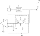
- FIG. 9 illustrates a block diagram 900 of an ultrasound device comprising a symmetric switch, according to a non-limiting embodiment of the present application.
- Symmetric switch 907 may be configured to block positive and negative voltages associated with the bipolar pulses generated by pulsing circuit 103 , thus preventing damage to receiving circuit 109 .
- symmetric switch 907 may comprise two transistors 910 and 912 .
- symmetric switch 907 may include any suitable number of transistors configured to block bipolar pulses during transmit mode.
- Transistors 910 and 912 may be of any type, such as metal-oxide-semiconductor field effect transistors (MOSFETs) including nMOS or pMOS, junction field effect transistors (JFETs), bipolar junction transistors (BJTs), metal-semiconductor field effect transistors (MESFETs), insulated gate field effect transistors (IGFETs), laterally diffused metal-oxide-semiconductor transistors (LDMOS), or any suitable combination thereof.
- MOSFETs metal-oxide-semiconductor field effect transistors
- JFETs junction field effect transistors
- BJTs bipolar junction transistors
- MEFETs metal-semiconductor field effect transistors
- IGFETs insulated gate field effect transistors
- LDMOS later
- both transistors 910 and 912 are nMOS.
- the gate of transistor 910 may be short-circuited to the gate of transistor 912 .
- a second terminal, other than the gate, of transistor 910 may be short-circuited to a second terminal, other than the gate, of transistor 912 .
- the source of transistor 910 may be short-circuited to the source of transistor 912 .
- the third terminal of transistor 912 for example, the drain, may be coupled between the output terminal of pulsing circuit 103 and a terminal of capacitive ultrasonic transducer 101 .
- the third terminal of transistor 910 for example, the drain, may be coupled to the input terminal of receiving circuit 109 .
- the drain of transistor 910 may be short-circuited to the input terminal of receiving circuit 109 .
- the body terminal of transistor 910 may be short-circuited to the source of transistor 910 and the body terminal of transistor 912 may be short-circuited to the source of transistor 912 .
- switching circuit 908 may be used to block bipolar pulses during transmit mode.
- Switching circuit 908 may comprise symmetric switch 907 and transistor 915 .
- Transistor 915 may be any suitable type of transistor.
- transistor 915 may be an nMOS.
- Transistor 915 may be configured to have the drain short-circuited to the input terminal of receiving circuit 109 .
- the source of transistor 915 may be short-circuited to a ground terminal.
- the body terminal of transistor 915 may be short-circuited to its source.
- the symmetric switch may comprise pMOS transistors.
- FIG. 11 illustrates a block diagram 1100 of an ultrasonic device comprising a symmetric switch, where the symmetric switch comprises two pMOS transistors 1110 and 1112 , according to a non-limiting embodiment of the present application. While FIG. 11 illustrates a symmetric switch comprising two pMOS transistors, any other suitable number of pMOS transistors may be used.
- Symmetric switch 1107 may be configured such that the gate of transistor 1110 may be short-circuited to the gate of transistor 1112 .
- a second terminal, other than the gate, of transistor 1110 may be short-circuited to a second terminal, other than the gate, of transistor 1112 .
- the source of transistor 1110 may be short-circuited to the source of transistor 1112 .
- the third terminal of transistor 1112 for example, the drain, may be coupled between the output terminal of pulsing circuit 103 and a terminal of capacitive ultrasonic transducer 101 .
- the third terminal of transistor 1110 for example, the drain, may be coupled to the input terminal of receiving circuit 109 .
- the drain of transistor 1110 may be short-circuited to the input terminal of receiving circuit 109 .
- the body terminal of transistor 1110 may be short-circuited to the source of transistor 1110 and the body terminal of transistor 1112 may be short-circuited to the source of transistor 1112 .
- switching circuit 1108 may comprise symmetric switch 1107 and transistor 915 .
- Switching circuit 908 may be controlled by any suitable type and number of control signals configured to block bipolar pulses generated by pulsing circuit 103 during transmit mode and further configured to couple capacitive ultrasonic transducer 101 to receiving circuit 109 during receive mode.
- FIG. 10 illustrates a timing diagram 1000 showing control signals configured to drive the symmetric switch of FIG. 9 , according to a non-limiting embodiment of the present application.
- Control signal 1002 may control the gates of transistors 910 and 912 via terminal G.
- Control signal 1004 may control the sources of transistors 910 and 912 via terminal S.
- Control signal 1006 may control the gate of transistor 915 via terminal G 2 .
- receiving circuit 109 may be turned on and off with control signal 1008 .
- control 1008 may enable/disable the voltage supply of receiving circuit 109 .
- switching circuit 908 may be configured to operate in receive mode.
- control signal 1002 may be greater than control signal 1004 .
- both control signals 1002 and 1004 may be greater than zero. In this way, both transistors may have a gate-source voltage greater than zero and hence may be configured to conduct electric currents.
- Control signal 1006 may be zero or below the threshold voltage of transistor 915 to maintain transistor 915 in a cutoff state.
- control signal 1008 may be set to a value that enables receiving circuit 109 .
- control signal 1008 may be set to a value that disables receiving circuit 109 .
- control signal 1002 may be set to a value equal to control signal 1004 . Consequently, transistors 910 and 912 may turn into their cutoff mode.
- control signal 1006 may be set to a value above the threshold voltage of transistor 915 . Consequently, the input terminal of receiving circuit 109 may be forced to a voltage equal to zero.
- control signals 1002 and 1004 may be set to a negative voltage. In some embodiments, control signals 1002 and 1004 may be set to a negative voltage simultaneously. In some embodiments the negative voltage may be equal to V N shown in FIG. 3 .
- control signals 1002 and 1004 may be set to zero or to the bias voltage of pulsing circuit 103 . In some embodiments, control signals 1002 and 1004 may be set to zero or to the bias voltage of pulsing circuit 103 simultaneously.
- control signal 1002 may be set to a voltage such that the gate-source voltages of transistors 910 and 912 are above threshold.
- control signal 1006 may be set to a value below the threshold voltage of transistor 915 , so that the voltage associated with the input terminal of receive circuit 109 may fluctuate freely.
- control signal 1008 may be set to a value that enables receiving circuit 109 .
- the receive mode may be defined by the time periods before t 0 and after t 5 and the transmit mode may be defined by the time period between t 0 and t 5 . In other embodiments, the receive mode may be defined by the time periods before t 1 and after t 4 and the transmit mode may be defined by the time period between t 1 and t 4 .
- t 0 may be equal to t 1 .
- t 1 may be equal to t 2 .
- t 3 may be equal to t 4 .
- t 4 may be equal to t 5 .
- aspects of the present application provide pulsing circuits configured to generate bipolar pulses that may be received without resulting in the saturation of the receiving circuit.
- receiving circuits may comprise components not designed to withstand the large positive and negative voltage spikes associated with the bipolar pulses.
- aspects of the present application provide symmetric switches configured to decouple the receiving circuit from the transmitting circuit, during a transmit mode, thus preventing damage to the receiving circuit caused by bipolar pulses.
- time-domain and space-domain apodized pulses requires the ability to control multi-level pulses.
- aspects of the present application provide feedback circuits configured to provide time-domain and space-domain apodization without resorting to additional supply voltages. Accordingly, incorporating additional supply voltages to the ultrasound devices may result in sizeable handheld ultrasound probes.
- some aspects may be embodied as one or more methods.
- the acts performed as part of the method may be ordered in any suitable way. Accordingly, embodiments may be constructed in which acts are performed in an order different than illustrated, which may include performing some acts simultaneously, even though shown as sequential acts in illustrative embodiments.
- the phrase “at least one,” in reference to a list of one or more elements, should be understood to mean at least one element selected from any one or more of the elements in the list of elements, but not necessarily including at least one of each and every element specifically listed within the list of elements and not excluding any combinations of elements in the list of elements.
- This definition also allows that elements may optionally be present other than the elements specifically identified within the list of elements to which the phrase “at least one” refers, whether related or unrelated to those elements specifically identified.
- the terms “approximately” and “about” may be used to mean within ⁇ 20% of a target value in some embodiments, within ⁇ 10% of a target value in some embodiments, within ⁇ 5% of a target value in some embodiments, and yet within ⁇ 2% of a target value in some embodiments.
- the terms “approximately” and “about” may include the target value.
Landscapes
- Engineering & Computer Science (AREA)
- Physics & Mathematics (AREA)
- Radar, Positioning & Navigation (AREA)
- Remote Sensing (AREA)
- Computer Networks & Wireless Communication (AREA)
- General Physics & Mathematics (AREA)
- Acoustics & Sound (AREA)
- Ultra Sonic Daignosis Equipment (AREA)
- Transducers For Ultrasonic Waves (AREA)
Abstract
Description
Claims (9)
Priority Applications (1)
| Application Number | Priority Date | Filing Date | Title |
|---|---|---|---|
| US16/035,552 US11061125B2 (en) | 2016-03-31 | 2018-07-13 | Symmetric receiver switch for bipolar pulser |
Applications Claiming Priority (3)
| Application Number | Priority Date | Filing Date | Title |
|---|---|---|---|
| US15/087,943 US9778348B1 (en) | 2016-03-31 | 2016-03-31 | Symmetric receiver switch for bipolar pulser |
| US15/659,134 US10094917B2 (en) | 2016-03-31 | 2017-07-25 | Symmetric receiver switch for bipolar pulser |
| US16/035,552 US11061125B2 (en) | 2016-03-31 | 2018-07-13 | Symmetric receiver switch for bipolar pulser |
Related Parent Applications (1)
| Application Number | Title | Priority Date | Filing Date |
|---|---|---|---|
| US15/659,134 Division US10094917B2 (en) | 2016-03-31 | 2017-07-25 | Symmetric receiver switch for bipolar pulser |
Publications (2)
| Publication Number | Publication Date |
|---|---|
| US20180321365A1 US20180321365A1 (en) | 2018-11-08 |
| US11061125B2 true US11061125B2 (en) | 2021-07-13 |
Family
ID=59929190
Family Applications (3)
| Application Number | Title | Priority Date | Filing Date |
|---|---|---|---|
| US15/087,943 Active US9778348B1 (en) | 2016-03-31 | 2016-03-31 | Symmetric receiver switch for bipolar pulser |
| US15/659,134 Active 2036-07-18 US10094917B2 (en) | 2016-03-31 | 2017-07-25 | Symmetric receiver switch for bipolar pulser |
| US16/035,552 Active 2037-05-19 US11061125B2 (en) | 2016-03-31 | 2018-07-13 | Symmetric receiver switch for bipolar pulser |
Family Applications Before (2)
| Application Number | Title | Priority Date | Filing Date |
|---|---|---|---|
| US15/087,943 Active US9778348B1 (en) | 2016-03-31 | 2016-03-31 | Symmetric receiver switch for bipolar pulser |
| US15/659,134 Active 2036-07-18 US10094917B2 (en) | 2016-03-31 | 2017-07-25 | Symmetric receiver switch for bipolar pulser |
Country Status (9)
| Country | Link |
|---|---|
| US (3) | US9778348B1 (en) |
| EP (1) | EP3435872B1 (en) |
| JP (1) | JP6975721B2 (en) |
| KR (1) | KR102403143B1 (en) |
| CN (1) | CN109069106B (en) |
| AU (1) | AU2017240043B2 (en) |
| CA (1) | CA3018967A1 (en) |
| TW (1) | TWI729108B (en) |
| WO (1) | WO2017173211A1 (en) |
Cited By (2)
| Publication number | Priority date | Publication date | Assignee | Title |
|---|---|---|---|---|
| US11294044B2 (en) | 2016-03-31 | 2022-04-05 | Bfly Operations, Inc. | Multilevel bipolar pulser |
| US12156762B2 (en) | 2021-04-01 | 2024-12-03 | Bfly Operations, Inc. | Apparatuses and methods for configuring ultrasound devices |
Families Citing this family (11)
| Publication number | Priority date | Publication date | Assignee | Title |
|---|---|---|---|---|
| US9778348B1 (en) | 2016-03-31 | 2017-10-03 | Butterfly Network, Inc. | Symmetric receiver switch for bipolar pulser |
| US10859687B2 (en) | 2016-03-31 | 2020-12-08 | Butterfly Network, Inc. | Serial interface for parameter transfer in an ultrasound device |
| US11154279B2 (en) * | 2016-03-31 | 2021-10-26 | Bfly Operations, Inc. | Transmit generator for controlling a multilevel pulser of an ultrasound device, and related methods and apparatus |
| KR20210005208A (en) | 2018-05-03 | 2021-01-13 | 버터플라이 네트워크, 인크. | Pressure port for ultrasonic transducer on CMOS sensor |
| WO2021016461A1 (en) | 2019-07-25 | 2021-01-28 | Butterfly Network, Inc. | Methods and apparatuses for turning on and off and adc driver in an ultrasound device |
| JP2021038981A (en) * | 2019-09-02 | 2021-03-11 | 株式会社日立製作所 | Measurement method using capacitance detection type ultrasonic transducer |
| WO2021055721A1 (en) * | 2019-09-19 | 2021-03-25 | Butterfly Network, Inc. | Symmetric receiver switch for ultrasound devices |
| US11815492B2 (en) | 2020-04-16 | 2023-11-14 | Bfly Operations, Inc. | Methods and circuitry for built-in self-testing of circuitry and/or transducers in ultrasound devices |
| US11808897B2 (en) | 2020-10-05 | 2023-11-07 | Bfly Operations, Inc. | Methods and apparatuses for azimuthal summing of ultrasound data |
| IT202100004466A1 (en) | 2021-02-25 | 2022-08-25 | St Microelectronics Srl | MULTILEVEL PULSE GENERATOR CIRCUIT AND PROCEDURE OF OPERATION OF A MULTILEVEL PULSE GENERATOR CIRCUIT |
| US12408895B2 (en) * | 2022-11-10 | 2025-09-09 | Fujifilm Corporation | Ultrasound probe and ultrasound diagnostic apparatus |
Citations (69)
| Publication number | Priority date | Publication date | Assignee | Title |
|---|---|---|---|---|
| US3643181A (en) | 1970-06-11 | 1972-02-15 | Us Army | Amplitude and/or frequency-modulated paramagnetic resonance oscillator |
| JPS6169212A (en) | 1984-09-12 | 1986-04-09 | Fujitsu Ltd | Switching circuit |
| JPS62240032A (en) | 1986-04-10 | 1987-10-20 | 株式会社東芝 | Ultrasonic diagnostic apparatus |
| US5487015A (en) | 1993-09-13 | 1996-01-23 | Rockwell International Corporation | Self-oscillating driver circuit for a quartz resonator of an angular rate sensor |
| US5608409A (en) | 1995-03-28 | 1997-03-04 | Rilling; Kenneth F. | Adaptive array with automatic loop gain control |
| JPH0974345A (en) | 1995-09-05 | 1997-03-18 | Fuji Electric Co Ltd | Insulated gate semiconductor element drive circuit |
| US5841693A (en) | 1996-04-25 | 1998-11-24 | Nec Corporation | Non-volatile memory using field effect transistors having dual floating gates for storing two bits per cell |
| US5929811A (en) | 1995-03-28 | 1999-07-27 | Rilling; Kenneth F. | Adaptive array with automatic loop gain control |
| US6241676B1 (en) | 1999-06-10 | 2001-06-05 | Agilent Technologies, Inc. | Ultrasound transmit waveforms having low harmonic content |
| US20020067208A1 (en) | 2000-12-05 | 2002-06-06 | Nippon Telegraph And Telephone Corporation | Transconductance amplifier, filter using the transconductance amplifier and tuning circuitry for transconductance amplifier in the filter |
| US6459743B1 (en) | 1998-08-07 | 2002-10-01 | Telefonaktiebolaget Lm Ericsson (Publ) | Digital reception with radio frequency sampling |
| US20030097071A1 (en) | 2001-11-21 | 2003-05-22 | Menachem Halmann | Method and system for PDA-based ultrasound system |
| US6653891B1 (en) | 2002-07-09 | 2003-11-25 | Intel Corporation | Voltage regulation |
| US20040037342A1 (en) | 2002-08-22 | 2004-02-26 | Blauvelt Henry A. | Grating-stabilized semiconductor laser |
| US20050007879A1 (en) | 2003-06-03 | 2005-01-13 | Masaru Nishida | Ultrasonic transmitter, ultrasonic transceiver and sounding apparatus |
| US20050040896A1 (en) | 2003-08-22 | 2005-02-24 | Koichi Yahagi | High frequency semiconductor integrated circuit device, wireless electric unit and wireless communication system |
| US20050131297A1 (en) | 2002-04-30 | 2005-06-16 | Matsushita Electric Industrial Co., Ltd. | Ultrasonic diagnostic equipment |
| US20050154300A1 (en) | 2003-12-30 | 2005-07-14 | Wodnicki Robert G. | Integrated low-voltage transmit/receive switch for ultrasound imaging system |
| US20050171431A1 (en) | 2004-01-21 | 2005-08-04 | Siemens Medical Solutions Usa, Inc. | Integrated low-power pw/cw transmitter |
| US20060012400A1 (en) | 2004-07-14 | 2006-01-19 | Nec Electronics Corporation | Electric potential switching circuit, flash memory with electric potential switching circuit, and method of switching electric potential |
| US20060058588A1 (en) | 2004-09-02 | 2006-03-16 | Proteus Biomedical, Inc. | Methods and apparatus for tissue activation and monitoring |
| US7103188B1 (en) | 1993-06-23 | 2006-09-05 | Owen Jones | Variable gain active noise cancelling system with improved residual noise sensing |
| US20070016026A1 (en) | 2005-06-29 | 2007-01-18 | Thomenius Kai E | Transmit and receive interface array for highly integrated ultrasound scanner |
| US20070083119A1 (en) | 2004-06-11 | 2007-04-12 | Olympus Corporation | Ultrasonic probe apparatus and ultrasonic diagnostic apparatus |
| US20070153937A1 (en) | 2003-10-23 | 2007-07-05 | Grigory Itkin | Power control circuitary for a mobile terminal application |
| US20070242567A1 (en) | 2005-12-07 | 2007-10-18 | Daft Christopher M | Multi-dimensional CMUT array with integrated beamformation |
| US7313053B2 (en) | 2003-03-06 | 2007-12-25 | General Electric Company | Method and apparatus for controlling scanning of mosaic sensor array |
| US20080021327A1 (en) | 2006-05-12 | 2008-01-24 | Tarek Hessin Ahmed El-Bialy | Ultrasound stimulation devices and techniques |
| US20080238532A1 (en) | 2007-03-30 | 2008-10-02 | Satoshi Hanazawa | Semiconductor integrated circuit device |
| US20080264171A1 (en) | 2007-04-26 | 2008-10-30 | General Electric Company | Reconfigurable array with multi-level transmitters |
| US20080283889A1 (en) | 2007-05-17 | 2008-11-20 | Keiichi Haraguchi | Semiconductor device |
| US20090096489A1 (en) | 2007-10-16 | 2009-04-16 | Broadcom Corporation | High voltage tolerant over-current detector |
| US7549961B1 (en) | 2003-07-31 | 2009-06-23 | Sonosite, Inc. | System and method supporting imaging and monitoring applications |
| US20090182233A1 (en) | 2008-01-10 | 2009-07-16 | Robert Gideon Wodnicki | Ultrasound System With Integrated Control Switches |
| US20090250729A1 (en) | 2004-09-15 | 2009-10-08 | Lemmerhirt David F | Capacitive micromachined ultrasonic transducer and manufacturing method |
| WO2009135255A1 (en) | 2008-05-07 | 2009-11-12 | Signostics Pty Ltd | Docking system for medical diagnostic scanning using a handheld device |
| US20100152587A1 (en) | 2008-12-17 | 2010-06-17 | General Electric Company | Systems and methods for operating a two-dimensional transducer array |
| CN201535683U (en) | 2009-11-12 | 2010-07-28 | 中环天仪股份有限公司 | Drive circuit of piezoelectric supersonic transducer |
| US20100317972A1 (en) | 2009-06-16 | 2010-12-16 | Charles Edward Baumgartner | Ultrasound transducer with improved acoustic performance |
| US20100315272A1 (en) | 2008-05-07 | 2010-12-16 | Colin Findlay Steele | Capacitive transducer circuit and method |
| US20110060225A1 (en) | 2009-09-09 | 2011-03-10 | General Electric Company | Ultrasound probe with integrated pulsers |
| US20120108963A1 (en) | 2010-10-28 | 2012-05-03 | Hitachi, Ltd. | Semiconductor Device and Ultrasonic Diagnostic Apparatus Using the Same |
| US20120169420A1 (en) | 2010-12-29 | 2012-07-05 | Stmicroelectronics (Shenzhen) R&D Co. Ltd. | Circuit and method for amplifying a digital signal |
| US8298144B2 (en) | 2006-06-23 | 2012-10-30 | Koninklijke Philips Electronics N.V. | Timing controller for combined photoacoustic and ultrasound imager |
| US8327521B2 (en) | 2007-09-17 | 2012-12-11 | Koninklijke Philips Electronics N.V. | Method for production and using a capacitive micro-machined ultrasonic transducer |
| CN102869959A (en) | 2010-04-28 | 2013-01-09 | 米托尔斯有限公司 | Ultrasonic Flow Meter |
| CN103028199A (en) | 2011-10-09 | 2013-04-10 | 北京汇福康医疗技术有限公司 | Monitoring method and monitoring device of ultrasound energy converter sound filed |
| US20130207113A1 (en) | 2012-02-10 | 2013-08-15 | E Ink Holdings Inc. | Electrostatic discharge protection structure for an active array substrate |
| CN103654852A (en) | 2012-09-25 | 2014-03-26 | 精工爱普生株式会社 | Integrated circuit apparatus, ultrasound measuring apparatus and ultrasound diagnosis apparatus |
| TW201417505A (en) | 2012-10-17 | 2014-05-01 | 財團法人工業技術研究院 | Capacitive load drive circuit and pulse excitation device |
| CN203616291U (en) | 2013-12-02 | 2014-05-28 | 河海大学常州校区 | Bipolar high-power pulse ultrasonic generator |
| US20140243614A1 (en) | 2013-02-26 | 2014-08-28 | Butterfly Network, Inc. | Transmissive imaging and related apparatus and methods |
| US20140288428A1 (en) | 2013-03-15 | 2014-09-25 | Butterfly Network, Inc. | Monolithic ultrasonic imaging devices, systems and methods |
| US8852103B2 (en) | 2011-10-17 | 2014-10-07 | Butterfly Network, Inc. | Transmissive imaging and related apparatus and methods |
| US20150032002A1 (en) | 2013-07-23 | 2015-01-29 | Butterfly Network, Inc. | Interconnectable ultrasound transducer probes and related methods and apparatus |
| US20150109057A1 (en) | 2013-10-22 | 2015-04-23 | Stmicroelectronics Sa | Resistive ladder |
| US20150297193A1 (en) | 2014-04-18 | 2015-10-22 | Butterfly Network, Inc. | Ultrasonic Imaging Compression Methods and Apparatus |
| US20150340023A1 (en) | 2012-11-28 | 2015-11-26 | B-K Medical Aps | Ultrasound Imaging Probe with Sigma-Delta Beamformer and Apodization Therein |
| WO2015189982A1 (en) | 2014-06-13 | 2015-12-17 | 株式会社日立製作所 | Switch circuit, ultrasonic contactor using same, and ultrasonic diagnosis apparatus |
| US20150374335A1 (en) | 2013-03-07 | 2015-12-31 | Sharp Kabushiki Kaisha | Ultrasound sensor element, ultrasound sensor array assembly, ultrasound transmit sensor element, imaging device, ultrasound transducer, and method of performing an ultrasound scan |
| US9229097B2 (en) | 2014-04-18 | 2016-01-05 | Butterfly Network, Inc. | Architecture of single substrate ultrasonic imaging devices, related apparatuses, and methods |
| US20160076933A1 (en) | 2014-09-15 | 2016-03-17 | Stmicroelectronics S.R.L. | Reception and transmission circuit for a capacitive micromachined ultrasonic transducer |
| WO2016057622A1 (en) | 2014-10-07 | 2016-04-14 | Butterfly Network, Inc. | Ultrasound signal processing circuitry and related apparatus and methods |
| WO2016057631A1 (en) | 2014-10-08 | 2016-04-14 | Butterfly Network, Inc. | Parameter loader for ultrasound probe and related apparatus and methods |
| US20160207760A1 (en) | 2013-03-15 | 2016-07-21 | Butterfly Network, Inc. | Complementary metal oxide semiconductor (cmos) ultrasonic transducers and methods for forming the same |
| US20160331353A1 (en) | 2015-05-15 | 2016-11-17 | Butterfly Network, Inc. | Autonomous ultrasound probe and related apparatus and methods |
| US20170104481A1 (en) * | 2015-10-08 | 2017-04-13 | Microchip Technology Inc. | Optimized CMOS Analog Switch |
| US9778348B1 (en) | 2016-03-31 | 2017-10-03 | Butterfly Network, Inc. | Symmetric receiver switch for bipolar pulser |
| US20170285155A1 (en) | 2016-03-31 | 2017-10-05 | Butterfly Network, Inc. | Multilevel bipolar pulser |
-
2016
- 2016-03-31 US US15/087,943 patent/US9778348B1/en active Active
-
2017
- 2017-03-31 JP JP2018550321A patent/JP6975721B2/en active Active
- 2017-03-31 CN CN201780025290.7A patent/CN109069106B/en active Active
- 2017-03-31 KR KR1020187031301A patent/KR102403143B1/en active Active
- 2017-03-31 EP EP17776738.1A patent/EP3435872B1/en active Active
- 2017-03-31 AU AU2017240043A patent/AU2017240043B2/en not_active Ceased
- 2017-03-31 TW TW106111106A patent/TWI729108B/en not_active IP Right Cessation
- 2017-03-31 WO PCT/US2017/025269 patent/WO2017173211A1/en not_active Ceased
- 2017-03-31 CA CA3018967A patent/CA3018967A1/en active Pending
- 2017-07-25 US US15/659,134 patent/US10094917B2/en active Active
-
2018
- 2018-07-13 US US16/035,552 patent/US11061125B2/en active Active
Patent Citations (87)
| Publication number | Priority date | Publication date | Assignee | Title |
|---|---|---|---|---|
| US3643181A (en) | 1970-06-11 | 1972-02-15 | Us Army | Amplitude and/or frequency-modulated paramagnetic resonance oscillator |
| JPS6169212A (en) | 1984-09-12 | 1986-04-09 | Fujitsu Ltd | Switching circuit |
| JPS62240032A (en) | 1986-04-10 | 1987-10-20 | 株式会社東芝 | Ultrasonic diagnostic apparatus |
| US7103188B1 (en) | 1993-06-23 | 2006-09-05 | Owen Jones | Variable gain active noise cancelling system with improved residual noise sensing |
| US5487015A (en) | 1993-09-13 | 1996-01-23 | Rockwell International Corporation | Self-oscillating driver circuit for a quartz resonator of an angular rate sensor |
| US5608409A (en) | 1995-03-28 | 1997-03-04 | Rilling; Kenneth F. | Adaptive array with automatic loop gain control |
| US5929811A (en) | 1995-03-28 | 1999-07-27 | Rilling; Kenneth F. | Adaptive array with automatic loop gain control |
| JPH0974345A (en) | 1995-09-05 | 1997-03-18 | Fuji Electric Co Ltd | Insulated gate semiconductor element drive circuit |
| US5841693A (en) | 1996-04-25 | 1998-11-24 | Nec Corporation | Non-volatile memory using field effect transistors having dual floating gates for storing two bits per cell |
| US6459743B1 (en) | 1998-08-07 | 2002-10-01 | Telefonaktiebolaget Lm Ericsson (Publ) | Digital reception with radio frequency sampling |
| US6241676B1 (en) | 1999-06-10 | 2001-06-05 | Agilent Technologies, Inc. | Ultrasound transmit waveforms having low harmonic content |
| US20020067208A1 (en) | 2000-12-05 | 2002-06-06 | Nippon Telegraph And Telephone Corporation | Transconductance amplifier, filter using the transconductance amplifier and tuning circuitry for transconductance amplifier in the filter |
| US20030097071A1 (en) | 2001-11-21 | 2003-05-22 | Menachem Halmann | Method and system for PDA-based ultrasound system |
| CN1649545A (en) | 2002-04-30 | 2005-08-03 | 松下电器产业株式会社 | Ultrasonic diagnostic instrument |
| US20050131297A1 (en) | 2002-04-30 | 2005-06-16 | Matsushita Electric Industrial Co., Ltd. | Ultrasonic diagnostic equipment |
| US6653891B1 (en) | 2002-07-09 | 2003-11-25 | Intel Corporation | Voltage regulation |
| US20040037342A1 (en) | 2002-08-22 | 2004-02-26 | Blauvelt Henry A. | Grating-stabilized semiconductor laser |
| US7313053B2 (en) | 2003-03-06 | 2007-12-25 | General Electric Company | Method and apparatus for controlling scanning of mosaic sensor array |
| US20050007879A1 (en) | 2003-06-03 | 2005-01-13 | Masaru Nishida | Ultrasonic transmitter, ultrasonic transceiver and sounding apparatus |
| US7549961B1 (en) | 2003-07-31 | 2009-06-23 | Sonosite, Inc. | System and method supporting imaging and monitoring applications |
| US20050040896A1 (en) | 2003-08-22 | 2005-02-24 | Koichi Yahagi | High frequency semiconductor integrated circuit device, wireless electric unit and wireless communication system |
| US20070153937A1 (en) | 2003-10-23 | 2007-07-05 | Grigory Itkin | Power control circuitary for a mobile terminal application |
| US20050154300A1 (en) | 2003-12-30 | 2005-07-14 | Wodnicki Robert G. | Integrated low-voltage transmit/receive switch for ultrasound imaging system |
| US7314445B2 (en) | 2003-12-30 | 2008-01-01 | General Electric Company | Integrated low-voltage transmit/receive switch for ultrasound imaging system |
| US20050171431A1 (en) | 2004-01-21 | 2005-08-04 | Siemens Medical Solutions Usa, Inc. | Integrated low-power pw/cw transmitter |
| US7883466B2 (en) | 2004-06-11 | 2011-02-08 | Olympus Corporation | Ultrasonic probe apparatus and ultrasonic diagnostic apparatus |
| US20070083119A1 (en) | 2004-06-11 | 2007-04-12 | Olympus Corporation | Ultrasonic probe apparatus and ultrasonic diagnostic apparatus |
| US20060012400A1 (en) | 2004-07-14 | 2006-01-19 | Nec Electronics Corporation | Electric potential switching circuit, flash memory with electric potential switching circuit, and method of switching electric potential |
| US20060058588A1 (en) | 2004-09-02 | 2006-03-16 | Proteus Biomedical, Inc. | Methods and apparatus for tissue activation and monitoring |
| US20090250729A1 (en) | 2004-09-15 | 2009-10-08 | Lemmerhirt David F | Capacitive micromachined ultrasonic transducer and manufacturing method |
| US7775979B2 (en) | 2005-06-29 | 2010-08-17 | General Electric Company | Transmit and receive interface array for highly integrated ultrasound scanner |
| US20070016026A1 (en) | 2005-06-29 | 2007-01-18 | Thomenius Kai E | Transmit and receive interface array for highly integrated ultrasound scanner |
| US20070242567A1 (en) | 2005-12-07 | 2007-10-18 | Daft Christopher M | Multi-dimensional CMUT array with integrated beamformation |
| US20080021327A1 (en) | 2006-05-12 | 2008-01-24 | Tarek Hessin Ahmed El-Bialy | Ultrasound stimulation devices and techniques |
| US8298144B2 (en) | 2006-06-23 | 2012-10-30 | Koninklijke Philips Electronics N.V. | Timing controller for combined photoacoustic and ultrasound imager |
| US20080238532A1 (en) | 2007-03-30 | 2008-10-02 | Satoshi Hanazawa | Semiconductor integrated circuit device |
| US20080264171A1 (en) | 2007-04-26 | 2008-10-30 | General Electric Company | Reconfigurable array with multi-level transmitters |
| US20080283889A1 (en) | 2007-05-17 | 2008-11-20 | Keiichi Haraguchi | Semiconductor device |
| US8327521B2 (en) | 2007-09-17 | 2012-12-11 | Koninklijke Philips Electronics N.V. | Method for production and using a capacitive micro-machined ultrasonic transducer |
| US20090096489A1 (en) | 2007-10-16 | 2009-04-16 | Broadcom Corporation | High voltage tolerant over-current detector |
| US20090182233A1 (en) | 2008-01-10 | 2009-07-16 | Robert Gideon Wodnicki | Ultrasound System With Integrated Control Switches |
| US20100315272A1 (en) | 2008-05-07 | 2010-12-16 | Colin Findlay Steele | Capacitive transducer circuit and method |
| US20110055447A1 (en) | 2008-05-07 | 2011-03-03 | Signostics Limited | Docking system for medical diagnostic scanning using a handheld device |
| WO2009135255A1 (en) | 2008-05-07 | 2009-11-12 | Signostics Pty Ltd | Docking system for medical diagnostic scanning using a handheld device |
| CN101745501A (en) | 2008-12-17 | 2010-06-23 | 通用电气公司 | Systems and methods for operating a two-dimensional transducer array |
| US20100152587A1 (en) | 2008-12-17 | 2010-06-17 | General Electric Company | Systems and methods for operating a two-dimensional transducer array |
| US20100317972A1 (en) | 2009-06-16 | 2010-12-16 | Charles Edward Baumgartner | Ultrasound transducer with improved acoustic performance |
| US20110060225A1 (en) | 2009-09-09 | 2011-03-10 | General Electric Company | Ultrasound probe with integrated pulsers |
| CN201535683U (en) | 2009-11-12 | 2010-07-28 | 中环天仪股份有限公司 | Drive circuit of piezoelectric supersonic transducer |
| CN102869959A (en) | 2010-04-28 | 2013-01-09 | 米托尔斯有限公司 | Ultrasonic Flow Meter |
| US20130047695A1 (en) | 2010-04-28 | 2013-02-28 | Jens Drachmann | Ultrasonic Flow Meter |
| US20120108963A1 (en) | 2010-10-28 | 2012-05-03 | Hitachi, Ltd. | Semiconductor Device and Ultrasonic Diagnostic Apparatus Using the Same |
| CN102545860A (en) | 2010-10-28 | 2012-07-04 | 株式会社日立制作所 | Semiconductor device and ultrasonic diagnostic apparatus using the same |
| US20120169420A1 (en) | 2010-12-29 | 2012-07-05 | Stmicroelectronics (Shenzhen) R&D Co. Ltd. | Circuit and method for amplifying a digital signal |
| CN103028199A (en) | 2011-10-09 | 2013-04-10 | 北京汇福康医疗技术有限公司 | Monitoring method and monitoring device of ultrasound energy converter sound filed |
| US8852103B2 (en) | 2011-10-17 | 2014-10-07 | Butterfly Network, Inc. | Transmissive imaging and related apparatus and methods |
| US20130207113A1 (en) | 2012-02-10 | 2013-08-15 | E Ink Holdings Inc. | Electrostatic discharge protection structure for an active array substrate |
| CN103654852A (en) | 2012-09-25 | 2014-03-26 | 精工爱普生株式会社 | Integrated circuit apparatus, ultrasound measuring apparatus and ultrasound diagnosis apparatus |
| EP2711094A2 (en) | 2012-09-25 | 2014-03-26 | Seiko Epson Corporation | Integrated circuit apparatus, ultrasound measuring apparatus, ultrasound probe and ultrasound diagnosis apparatus |
| TW201417505A (en) | 2012-10-17 | 2014-05-01 | 財團法人工業技術研究院 | Capacitive load drive circuit and pulse excitation device |
| US20150340023A1 (en) | 2012-11-28 | 2015-11-26 | B-K Medical Aps | Ultrasound Imaging Probe with Sigma-Delta Beamformer and Apodization Therein |
| US20140243614A1 (en) | 2013-02-26 | 2014-08-28 | Butterfly Network, Inc. | Transmissive imaging and related apparatus and methods |
| US20150374335A1 (en) | 2013-03-07 | 2015-12-31 | Sharp Kabushiki Kaisha | Ultrasound sensor element, ultrasound sensor array assembly, ultrasound transmit sensor element, imaging device, ultrasound transducer, and method of performing an ultrasound scan |
| US20160207760A1 (en) | 2013-03-15 | 2016-07-21 | Butterfly Network, Inc. | Complementary metal oxide semiconductor (cmos) ultrasonic transducers and methods for forming the same |
| US20140288428A1 (en) | 2013-03-15 | 2014-09-25 | Butterfly Network, Inc. | Monolithic ultrasonic imaging devices, systems and methods |
| US9327142B2 (en) | 2013-03-15 | 2016-05-03 | Butterfly Network, Inc. | Monolithic ultrasonic imaging devices, systems and methods |
| US9351706B2 (en) | 2013-07-23 | 2016-05-31 | Butterfly Network, Inc. | Interconnectable ultrasound transducer probes and related methods and apparatus |
| US20150032002A1 (en) | 2013-07-23 | 2015-01-29 | Butterfly Network, Inc. | Interconnectable ultrasound transducer probes and related methods and apparatus |
| US20150109057A1 (en) | 2013-10-22 | 2015-04-23 | Stmicroelectronics Sa | Resistive ladder |
| CN203616291U (en) | 2013-12-02 | 2014-05-28 | 河海大学常州校区 | Bipolar high-power pulse ultrasonic generator |
| US20150297193A1 (en) | 2014-04-18 | 2015-10-22 | Butterfly Network, Inc. | Ultrasonic Imaging Compression Methods and Apparatus |
| US9229097B2 (en) | 2014-04-18 | 2016-01-05 | Butterfly Network, Inc. | Architecture of single substrate ultrasonic imaging devices, related apparatuses, and methods |
| US20170188996A1 (en) | 2014-06-13 | 2017-07-06 | Hitachi, Ltd. | Switch circuit, ultrasound probe using the same, and ultrasonic diagnosis apparatus |
| WO2015189982A1 (en) | 2014-06-13 | 2015-12-17 | 株式会社日立製作所 | Switch circuit, ultrasonic contactor using same, and ultrasonic diagnosis apparatus |
| US20160076933A1 (en) | 2014-09-15 | 2016-03-17 | Stmicroelectronics S.R.L. | Reception and transmission circuit for a capacitive micromachined ultrasonic transducer |
| CN105425227A (en) | 2014-09-15 | 2016-03-23 | 意法半导体股份有限公司 | Reception and transmission circuit for a capacitive micromachined ultrasonic transducer |
| WO2016057622A1 (en) | 2014-10-07 | 2016-04-14 | Butterfly Network, Inc. | Ultrasound signal processing circuitry and related apparatus and methods |
| WO2016057631A1 (en) | 2014-10-08 | 2016-04-14 | Butterfly Network, Inc. | Parameter loader for ultrasound probe and related apparatus and methods |
| US20160331353A1 (en) | 2015-05-15 | 2016-11-17 | Butterfly Network, Inc. | Autonomous ultrasound probe and related apparatus and methods |
| US20170104481A1 (en) * | 2015-10-08 | 2017-04-13 | Microchip Technology Inc. | Optimized CMOS Analog Switch |
| US9778348B1 (en) | 2016-03-31 | 2017-10-03 | Butterfly Network, Inc. | Symmetric receiver switch for bipolar pulser |
| US20170285155A1 (en) | 2016-03-31 | 2017-10-05 | Butterfly Network, Inc. | Multilevel bipolar pulser |
| US20170285150A1 (en) | 2016-03-31 | 2017-10-05 | Butterfly Network, Inc. | Symmetric receiver switch for bipolar pulser |
| US20170322293A1 (en) | 2016-03-31 | 2017-11-09 | Butterfly Network, Inc. | Symmetric receiver switch for bipolar pulser |
| US10082565B2 (en) | 2016-03-31 | 2018-09-25 | Butterfly Network, Inc. | Multilevel bipolar pulser |
| US10094917B2 (en) | 2016-03-31 | 2018-10-09 | Butterfly Network, Inc. | Symmetric receiver switch for bipolar pulser |
| US20180364342A1 (en) | 2016-03-31 | 2018-12-20 | Butterfly Network, Inc. | Multilevel bipolar pulser |
Non-Patent Citations (17)
| Title |
|---|
| Agarwal et al., Single-Chip Solution for Ultrasound Imaging Systems: Initial Results. 2007 IEEE Ultrasonics Symposium. Oct. 1, 2007;1563-6. |
| Chen et al., Ultrasonic Imaging Front-End Design for CMUT: A 3-Leve1 30Vpp Pulse-Shaping Pulser with Improved Efficiency and a Noise-Optimized Receiver. IEEE Asian Solid-State Circuits Conference. Nov. 12-14, 2012;173-6. |
| Cheng et al., An Efficient Electrical Addressing Method Using Through-Wafer Vias for Two-Dimensional Ultrasonic Arrays. 2000 IEEE Ultrasonics Symposium. 2000;2:1179-82. |
| Cheng et al., CMUT-in-CMOS ultrasonic transducer arrays with on-chip electronics. Transducers 2009. IEEE. Jun. 21, 2009;1222-5. |
| Cheng et al., Electrical Through-Wafer Interconnects with Sub-PicoFarad Parasitic Capacitance. 2001 Microelectromechan Syst Conf. Aug. 24, 2001;18-21. |
| Daft et al., 5F-3 a Matrix Transducer Design with Improved Image Quality and Acquisition Rate. 2007 IEEE Ultrasonics Symposium. Oct. 1, 2007;411-5. |
| Daft et al., Microfabricated Ultrasonic Transducers Monolithically Integrated with High Voltage Electronics. 2004 IEEE Ultrasonics Symposium. Aug. 23, 2004;1:493-6. |
| Extended European Search Report dated Oct. 25, 2019 in connection with European Application No. 17776733.2. |
| Extended European Search Report dated Oct. 25, 2019 in connection with European Application No. 17776738.1. |
| Gurun et al., Front-end CMOS electronics for monolithic integration with CMUT arrays: circuit design and initial experimental results. Proc Ultrason Symp. 2008;390-3. |
| International Preliminary Report on Patentability dated Oct. 11, 2018 in connection with International Application No. PCT/US2017/025269. |
| International Search Report and Written Opinion dated Jan. 4, 2021 in connection with International Application No. PCT/US2020/051453. |
| International Search Report and Written Opinion dated Jun. 16, 2017 in connection with International Application No. PCT/US2017/025269. |
| International Search Report and Written Opinion dated Nov. 13, 2014 in connection with International Application No. PCT/US2014/032803. |
| Khuri-Yakub B et al., Miniaturized Ultrasound Imaging Probes Enabled by CMUT Arrays with Integrated Frontend Electronic Circuits. Conf Proc IEEE Eng Med Biol Soc. 2010;1:5987-90. doi:10.1109/IEMBS.2010.5627580. Epub Dec. 6, 2010. 13 pages. |
| Kim et al., Design and Test of a Fully Controllable 64x128 2-D CMUT Array Integrated with Reconfigurable Frontend ASICs for Volumetric Ultrasound Imaging. IEEE. International Ultrasonics Symposium Proceedings. Oct. 7-10, 2012;77-80. doi:10.1109/ULTSYM.2012.0019. |
| Wygant et al., 50 kHz Capacitive Micromachined Ultrasonic Transducers for Generation of Highly Directional Sound with Parametric Arrays. IEEE Transactions on Ultrasonics, Ferroelectrics and Frequency Control. Jan. 2009; 56(1): 193-203. |
Cited By (3)
| Publication number | Priority date | Publication date | Assignee | Title |
|---|---|---|---|---|
| US11294044B2 (en) | 2016-03-31 | 2022-04-05 | Bfly Operations, Inc. | Multilevel bipolar pulser |
| US11768282B2 (en) | 2016-03-31 | 2023-09-26 | BFLY Operations, Inc | Multilevel bipolar pulser |
| US12156762B2 (en) | 2021-04-01 | 2024-12-03 | Bfly Operations, Inc. | Apparatuses and methods for configuring ultrasound devices |
Also Published As
| Publication number | Publication date |
|---|---|
| JP2019514256A (en) | 2019-05-30 |
| EP3435872C0 (en) | 2023-06-07 |
| TWI729108B (en) | 2021-06-01 |
| CN109069106A (en) | 2018-12-21 |
| TW201809719A (en) | 2018-03-16 |
| US20180321365A1 (en) | 2018-11-08 |
| JP6975721B2 (en) | 2021-12-01 |
| WO2017173211A1 (en) | 2017-10-05 |
| AU2017240043A1 (en) | 2018-10-11 |
| EP3435872A1 (en) | 2019-02-06 |
| US10094917B2 (en) | 2018-10-09 |
| US20170322293A1 (en) | 2017-11-09 |
| AU2017240043B2 (en) | 2021-12-16 |
| KR102403143B1 (en) | 2022-05-27 |
| EP3435872B1 (en) | 2023-06-07 |
| EP3435872A4 (en) | 2019-11-27 |
| US20170285150A1 (en) | 2017-10-05 |
| CA3018967A1 (en) | 2017-10-05 |
| KR20180127463A (en) | 2018-11-28 |
| US9778348B1 (en) | 2017-10-03 |
| CN109069106B (en) | 2022-03-08 |
Similar Documents
| Publication | Publication Date | Title |
|---|---|---|
| US11768282B2 (en) | Multilevel bipolar pulser | |
| US11061125B2 (en) | Symmetric receiver switch for bipolar pulser | |
| US11921240B2 (en) | Symmetric receiver switch for ultrasound devices | |
| US20050154300A1 (en) | Integrated low-voltage transmit/receive switch for ultrasound imaging system | |
| US20100321089A1 (en) | Complementary high voltage switched current source integrated circuit | |
| KR100416686B1 (en) | Integrated circuit for generating high voltage pulse for use in a medical ultrasound diagnostic system | |
| US20120209120A1 (en) | Integrated Ultrasound Transmitter with Cascode Trimming |
Legal Events
| Date | Code | Title | Description |
|---|---|---|---|
| FEPP | Fee payment procedure |
Free format text: ENTITY STATUS SET TO UNDISCOUNTED (ORIGINAL EVENT CODE: BIG.); ENTITY STATUS OF PATENT OWNER: LARGE ENTITY |
|
| FEPP | Fee payment procedure |
Free format text: ENTITY STATUS SET TO SMALL (ORIGINAL EVENT CODE: SMAL); ENTITY STATUS OF PATENT OWNER: LARGE ENTITY |
|
| STPP | Information on status: patent application and granting procedure in general |
Free format text: DOCKETED NEW CASE - READY FOR EXAMINATION |
|
| AS | Assignment |
Owner name: BUTTERFLY NETWORK, INC., CONNECTICUT Free format text: ASSIGNMENT OF ASSIGNORS INTEREST;ASSIGNORS:CHEN, KAILIANG;RALSTON, TYLER S.;FIFE, KEITH G.;SIGNING DATES FROM 20160420 TO 20160429;REEL/FRAME:047460/0685 |
|
| FEPP | Fee payment procedure |
Free format text: ENTITY STATUS SET TO UNDISCOUNTED (ORIGINAL EVENT CODE: BIG.); ENTITY STATUS OF PATENT OWNER: LARGE ENTITY |
|
| STPP | Information on status: patent application and granting procedure in general |
Free format text: RESPONSE TO NON-FINAL OFFICE ACTION ENTERED AND FORWARDED TO EXAMINER |
|
| STPP | Information on status: patent application and granting procedure in general |
Free format text: NOTICE OF ALLOWANCE MAILED -- APPLICATION RECEIVED IN OFFICE OF PUBLICATIONS |
|
| STPP | Information on status: patent application and granting procedure in general |
Free format text: AWAITING TC RESP., ISSUE FEE NOT PAID |
|
| STPP | Information on status: patent application and granting procedure in general |
Free format text: NOTICE OF ALLOWANCE MAILED -- APPLICATION RECEIVED IN OFFICE OF PUBLICATIONS |
|
| STPP | Information on status: patent application and granting procedure in general |
Free format text: PUBLICATIONS -- ISSUE FEE PAYMENT RECEIVED |
|
| STPP | Information on status: patent application and granting procedure in general |
Free format text: PUBLICATIONS -- ISSUE FEE PAYMENT VERIFIED |
|
| STCF | Information on status: patent grant |
Free format text: PATENTED CASE |
|
| AS | Assignment |
Owner name: BFLY OPERATIONS, INC., CONNECTICUT Free format text: CHANGE OF NAME;ASSIGNOR:BUTTERFLY NETWORK, INC.;REEL/FRAME:059369/0969 Effective date: 20210212 |
|
| FEPP | Fee payment procedure |
Free format text: ENTITY STATUS SET TO SMALL (ORIGINAL EVENT CODE: SMAL); ENTITY STATUS OF PATENT OWNER: SMALL ENTITY |
|
| MAFP | Maintenance fee payment |
Free format text: PAYMENT OF MAINTENANCE FEE, 4TH YR, SMALL ENTITY (ORIGINAL EVENT CODE: M2551); ENTITY STATUS OF PATENT OWNER: SMALL ENTITY Year of fee payment: 4 |