US11035036B2 - Method of forming copper alloy sputtering targets with refined shape and microstructure - Google Patents
Method of forming copper alloy sputtering targets with refined shape and microstructure Download PDFInfo
- Publication number
- US11035036B2 US11035036B2 US16/247,232 US201916247232A US11035036B2 US 11035036 B2 US11035036 B2 US 11035036B2 US 201916247232 A US201916247232 A US 201916247232A US 11035036 B2 US11035036 B2 US 11035036B2
- Authority
- US
- United States
- Prior art keywords
- billet
- copper
- heat treatment
- copper manganese
- forging
- Prior art date
- Legal status (The legal status is an assumption and is not a legal conclusion. Google has not performed a legal analysis and makes no representation as to the accuracy of the status listed.)
- Active, expires
Links
Images


Classifications
-
- B—PERFORMING OPERATIONS; TRANSPORTING
- B21—MECHANICAL METAL-WORKING WITHOUT ESSENTIALLY REMOVING MATERIAL; PUNCHING METAL
- B21J—FORGING; HAMMERING; PRESSING METAL; RIVETING; FORGE FURNACES
- B21J1/00—Preparing metal stock or similar ancillary operations prior, during or post forging, e.g. heating or cooling
- B21J1/003—Selecting material
-
- B—PERFORMING OPERATIONS; TRANSPORTING
- B21—MECHANICAL METAL-WORKING WITHOUT ESSENTIALLY REMOVING MATERIAL; PUNCHING METAL
- B21C—MANUFACTURE OF METAL SHEETS, WIRE, RODS, TUBES, PROFILES OR LIKE SEMI-MANUFACTURED PRODUCTS OTHERWISE THAN BY ROLLING; AUXILIARY OPERATIONS USED IN CONNECTION WITH METAL-WORKING WITHOUT ESSENTIALLY REMOVING MATERIAL
- B21C23/00—Extruding metal; Impact extrusion
- B21C23/001—Extruding metal; Impact extrusion to improve the material properties, e.g. lateral extrusion
-
- B—PERFORMING OPERATIONS; TRANSPORTING
- B21—MECHANICAL METAL-WORKING WITHOUT ESSENTIALLY REMOVING MATERIAL; PUNCHING METAL
- B21J—FORGING; HAMMERING; PRESSING METAL; RIVETING; FORGE FURNACES
- B21J1/00—Preparing metal stock or similar ancillary operations prior, during or post forging, e.g. heating or cooling
- B21J1/02—Preliminary treatment of metal stock without particular shaping, e.g. salvaging segregated zones, forging or pressing in the rough
-
- B—PERFORMING OPERATIONS; TRANSPORTING
- B21—MECHANICAL METAL-WORKING WITHOUT ESSENTIALLY REMOVING MATERIAL; PUNCHING METAL
- B21J—FORGING; HAMMERING; PRESSING METAL; RIVETING; FORGE FURNACES
- B21J1/00—Preparing metal stock or similar ancillary operations prior, during or post forging, e.g. heating or cooling
- B21J1/04—Shaping in the rough solely by forging or pressing
-
- B—PERFORMING OPERATIONS; TRANSPORTING
- B21—MECHANICAL METAL-WORKING WITHOUT ESSENTIALLY REMOVING MATERIAL; PUNCHING METAL
- B21J—FORGING; HAMMERING; PRESSING METAL; RIVETING; FORGE FURNACES
- B21J1/00—Preparing metal stock or similar ancillary operations prior, during or post forging, e.g. heating or cooling
- B21J1/06—Heating or cooling methods or arrangements specially adapted for performing forging or pressing operations
-
- C—CHEMISTRY; METALLURGY
- C22—METALLURGY; FERROUS OR NON-FERROUS ALLOYS; TREATMENT OF ALLOYS OR NON-FERROUS METALS
- C22C—ALLOYS
- C22C9/00—Alloys based on copper
- C22C9/05—Alloys based on copper with manganese as the next major constituent
-
- C—CHEMISTRY; METALLURGY
- C22—METALLURGY; FERROUS OR NON-FERROUS ALLOYS; TREATMENT OF ALLOYS OR NON-FERROUS METALS
- C22F—CHANGING THE PHYSICAL STRUCTURE OF NON-FERROUS METALS AND NON-FERROUS ALLOYS
- C22F1/00—Changing the physical structure of non-ferrous metals or alloys by heat treatment or by hot or cold working
- C22F1/08—Changing the physical structure of non-ferrous metals or alloys by heat treatment or by hot or cold working of copper or alloys based thereon
-
- C—CHEMISTRY; METALLURGY
- C23—COATING METALLIC MATERIAL; COATING MATERIAL WITH METALLIC MATERIAL; CHEMICAL SURFACE TREATMENT; DIFFUSION TREATMENT OF METALLIC MATERIAL; COATING BY VACUUM EVAPORATION, BY SPUTTERING, BY ION IMPLANTATION OR BY CHEMICAL VAPOUR DEPOSITION, IN GENERAL; INHIBITING CORROSION OF METALLIC MATERIAL OR INCRUSTATION IN GENERAL
- C23C—COATING METALLIC MATERIAL; COATING MATERIAL WITH METALLIC MATERIAL; SURFACE TREATMENT OF METALLIC MATERIAL BY DIFFUSION INTO THE SURFACE, BY CHEMICAL CONVERSION OR SUBSTITUTION; COATING BY VACUUM EVAPORATION, BY SPUTTERING, BY ION IMPLANTATION OR BY CHEMICAL VAPOUR DEPOSITION, IN GENERAL
- C23C14/00—Coating by vacuum evaporation, by sputtering or by ion implantation of the coating forming material
- C23C14/22—Coating by vacuum evaporation, by sputtering or by ion implantation of the coating forming material characterised by the process of coating
- C23C14/34—Sputtering
- C23C14/3407—Cathode assembly for sputtering apparatus, e.g. Target
- C23C14/3414—Metallurgical or chemical aspects of target preparation, e.g. casting, powder metallurgy
Definitions
- the present disclosure generally relates to copper manganese alloys and methods of forming copper manganese alloys. More specifically, the present disclosure relates to copper manganese alloys with refined shape and microstructures. In some embodiments, the copper manganese alloys may be formed into sputtering targets and used in various sputtering applications.
- PVD Physical vapor deposition
- FIG. 1 A schematic diagram of a portion of an exemplary sputtering assembly is shown in FIG. 1 .
- a sputtering assembly 10 comprises a backing plate 12 having a sputtering target 14 bonded thereto.
- a semiconductor wafer 18 is positioned within the assembly and is spaced from a sputtering surface 16 of the sputtering target 14 .
- particles or sputtered material 22 is displaced from the surface 16 of the sputtering target 14 and deposits on the surface of the semiconductor wafer 18 to form a coating (or thin film) 20 on the wafer.
- the sputtering assembly 10 depicted in FIG. 1 is an example configuration since, for example, both the target 14 and the backing plate 12 can be any suitable size or shape.
- the physical vapor deposition apparatus 10 may include the sputtering target 14 without the backing plate 12 . This configuration is referred to as a monolithic configuration.
- Various metals and alloys can be deposited using PVD technology, including for example Al, Ti, Cu, Ta, Ni, Mo, Au, Ag, Pt, and alloys of these elements.
- One such alloy is copper manganese (“CuMn”) which has been used in sputtering targets to form, for example, various metal interconnects used in the semiconductor industry.
- a sputtering target may be formed or forged from a metal or metal alloy billet.
- the use of various casting techniques that are characterized by a slower cooling rate can be advantageous to reduce the overall impurity of the billets and obtain cast billets, and thus sputtering targets, with higher purity.
- slower cooling during casting can result in large microstructures that can be detrimental during further processing. Therefore, there is a desire in the industry for increasingly refined metal and metal alloys and methods for forming such refined metal and metal alloys, for example as billets.
- Various aspects of the present disclosure relate to a method of forming a copper manganese sputtering target.
- the method includes subjecting a copper manganese billet to a first unidirectional forcing step such that a number of grains of the copper manganese billet are increased by at least a factor of 10.
- the method also includes heating the copper manganese billet at a temperature from about 650° C. to about 750° C. for from about 1 hour to about 3 hours in a first heat treatment step.
- the method also includes subjecting the copper manganese billet to a second unidirectional forging step such that the height of the billet is reduced by from about 40 percent to 95 percent.
- the method also includes heating the copper manganese billet at a temperature from about 500° C. to about 650° C. for from about 4 hours to about 8 hours in a second heat treatment step to form a copper alloy.
- Various aspects of the present disclosure relate to a method of forming a copper alloy sputtering target.
- the method includes subjecting a copper alloy billet to a first forging step such that a number of grains of the copper alloy billet are increased by at least a factor of 10.
- the method also includes heating the copper alloy billet after the first forging step in a first heat treatment step at a temperature and for a time sufficient to achieve 100 percent recrystallization of the copper alloy.
- the method also includes subjecting the copper alloy billet to a second forging step such that a height of the copper alloy billet is reduced by from about 40 percent to 95 percent.
- the method also includes heating the copper alloy billet after the second forging step in a second heat treatment step at a temperature and for a time sufficient to achieve a substantially refined grain structure.
- the method also includes forming the copper alloy billet into a copper alloy sputtering target.
- FIG. 1 is a schematic diagram of a portion of an exemplary sputtering assembly, according to some embodiments.
- FIG. 2 is a perspective diagram of an exemplary billet.
- FIG. 3 is a block flow diagram of a method of forming a copper manganese alloy, according to some embodiments.
- FIGS. 4A-C are photographs showing the effect of conventional processing methods on a copper manganese alloy.
- FIG. 5 is a photograph showing the effect of two-step forging process, according to some embodiments.
- FIGS. 6A-C are photographs showing the effect of an additional heat treatment step after a 25% forging process, according to some embodiments.
- FIGS. 7A-C are photographs showing the effect of an additional heat treatment step after a 17% forging process, according to some embodiments.
- FIGS. 8A-C are photographs showing the effect of an additional heat treatment step after a 12% forging process, according to some embodiments.
- FIG. 9 is a graph illustrating a relationship between the heat treatment temperature and percent forging/reduction in the first forging step, according to some embodiments.
- FIGS. 10A-B are micrographs of grain structures of various large-scale copper manganese alloy billets, according to some embodiments.
- FIGS. 10C-D are graphs illustrating an R ratio and grain size, respectively, for the copper manganese alloys of FIGS. 10A-B , according to some embodiments.
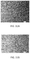
- FIGS. 11A-B are micrographs of the copper manganese alloys of FIGS. 10A-B after additional ECAE processing, according to some embodiments.
- FIG. 12A is a graph of the R ratio for copper manganese alloy billets, according to some embodiments.
- FIG. 12B is a graph of the grain size for copper manganese alloy billets, according to some embodiments.
- Disclosed herein is a copper manganese alloy for use, for example, in a sputtering target. Also disclosed herein are methods of forming copper manganese alloys. More specifically, disclosed herein are methods of forming copper manganese alloys with refined shape and refined, uniform microstructure.
- slow cooling refers to controlled or natural cooling of a cast copper manganese material from its melting temperature to an ambient temperature. During slow cooling, the cast material remains in the same crucible as used during the heating and melting phases and is allowed to cool within the crucible. This technique is opposed to other, faster cooling techniques such as quenching or pouring of the molten material from a first crucible to a second crucible with a significantly lower temperature than that of the molten material.
- Subjecting the copper manganese material to slow cooling may contribute to misshapen billets, increased cracking in billets, and various other defects during further plastic deformation, for example as the billet is processed to form a sputtering target.
- This slow cooling may reduce the overall impurity of the billets, enabling cast billets with higher purities to be obtained.
- slow cooling can result in large microstructures that can be detrimental during further processing.
- the alloys and methods disclosed herein produce copper manganese alloys having improved shape, reduced cracking and/or reduced defects during further plastic deformation.
- the copper manganese alloy includes copper as a primary component and manganese as a secondary component. Copper, as the primary component, is present in a higher weight percentage than manganese, which is a secondary component.
- the copper manganese alloy can include greater than 90 wt. %, greater than 98 wt. %, or greater than 99 wt. % copper, and less than 10 wt. %, less than 2.0 wt. %, less than 1.0 wt. % manganese, less than 0.1 wt. % manganese or less than 0.01 wt. % manganese.
- the copper manganese alloy may include copper, manganese and one or more additional secondary components.
- the copper manganese alloy may consist of copper, manganese and inevitable impurities, such as oxygen, carbon and other trace elements.
- the copper manganese alloy may have a refined microstructure.
- the amount of refinement of the microstructure can be characterized by a ratio, R, of the cross-sectional area of a billet over the average area of grains in that given cross-section.
- R can be defined as the total number of grains per billet cross-section.
- the cross-sectional area of the billet is the area of a face F of the billet when the billet is cut in half at diameter D along its height H (i.e., the cross-sectional area taken perpendicular to the bases of a cylindrical billet).
- the microstructure of the copper manganese alloy is characterized such that it has a ratio R greater than or equal to about 500.
- the copper manganese alloy may have a ratio R greater than 500, which, for example, is equivalent to greater than 500 grains per billet cross-section.
- a cylindrical billet with a height of 10 inches and a diameter of 10 inches has a cross-sectional area of 100 in 2 or 64,500 mm 2 . If the average diameter of grains in that billet is about 12.82 mm or 0.5 in, the average area of grains would be about 130 mm 2 or 0.2 in 2 . Therefore, the ratio R would be about 500 (i.e., there would be about 500 grains in the given cross-sectional area).
- the copper manganese alloy may have a ratio R greater than 1,000, greater than 10,000, greater than 100,000, greater than 1,000,000, or greater than 10,000,000.
- the billet has a certain, minimum number of grains required for a given billet size to facilitate isotropic and uniform deformation in all directions during forging.
- the copper manganese alloy may have an average grain size that is less than about 150 ⁇ m in diameter, less than about 100 ⁇ m in diameter, less than about 80 ⁇ m in diameter, less than about 50 ⁇ m in diameter, less than about 25 ⁇ m in diameter, or less than about 1 ⁇ m in diameter.
- the average grain size of a given billet will vary depending on the size and/or the cross-sectional area of the billet.
- the copper manganese alloy billet can have a refined shape.
- the billet may have a top face and/or a bottom face that is substantially equiaxed, circular, or rounded in shape.
- the top face and/or the bottom face of the billet may have approximately equal dimensions in all directions.
- the diameter of the top face and/or the bottom face in one direction is approximately equal to the diameter of the top face and/or the bottom face in the opposite/perpendicular direction.
- the top face and bottom face of the billet are uniform and/or smooth in texture.
- the billet may also be formed such that there may be no substantial protrusions detectable at the edges of the billet.
- a method 100 of forming a copper manganese alloy is shown in FIG. 3 .
- the method 100 includes forming a starting material in an initial processing step 110 .
- a copper material may be cast into a billet form using various casting techniques in combination with slow cooling, as described above.
- the copper material may include additives, such as other elements, which alloy with the copper to form a copper alloy.
- the copper material may include copper as a primary component and one or more elements as a secondary component.
- the copper material may include manganese as a secondary component.
- the copper manganese material may be formed using standard casting practices for a copper alloy including both copper and manganese.
- the copper manganese alloy is subjected to a first processing step 102 .
- the first processing step 102 includes a first forging step 112 and a first heat treatment step 114 .
- the first forging step 112 may include reducing the height of the copper manganese billet by from about 10% to about 33%.
- the first forging step 112 may include from a 10% reduction to a 25% reduction, from a 12% reduction to a 25% reduction, from about a 15% reduction to a 25% reduction, or from a 17% reduction to a 25% reduction in height of the copper manganese billet.
- the first forging step 112 is unidirectional forging or uniaxial forging such that the billet is forged along one plane or axis.
- the grain structure may be refined by a factor of at least about 10 during the first forging step 112 such that the total existing number of grains in the copper manganese billet increases by a factor of at least about 10 as a result of the first forging step 112 .
- the total number of grains in the copper manganese billet is increased by at least a factor of 10, as compared to the total number of grains in the copper manganese billet prior to forging.
- a material having a total of about 10 grains before the first forging step 112 will have a total of at least about 100 grains after the first forging step 112 .
- the first heat treatment step 114 may include heating the copper manganese billet at a temperature from about 650° C. to about 750° C., from about 675° C. to about 750° C., or from about 675° C. to about 700° C. for a period from about 0.5 hour to about 3 hours or for a period of about 1.5 to about 2 hours.
- the copper manganese billet may be heated at a temperature of about 700° C. for a period of about 2 hours.
- the first heat treatment step 114 may be carried out for a sufficient time to reach temperature homogeneity and equilibrium within the billet.
- the first heat treatment step 114 may be carried out at a sufficient temperature and time such that the grains do not regrow. In yet other embodiments, the first heat treatment step 114 may be carried out at a temperature and time sufficient to obtain from about 80% to 100% recrystallization of the existing grain structure, from about 90% to 100% recrystallization of the existing grain structure, or full recrystallization of the existing grain structure. In some examples, the grain structure may be refined by a factor of at least about 10 such that the total existing number of grains in the copper manganese billet increases by a factor of at least about 10, as described above, as a result of the first heat treatment step 114 .
- a copper manganese billet having a total of about 100 grains in a given cross-section before the first heat treatment step 114 will have a total of at least about 1,000 grains after the first heat treatment step.
- the grain structure may be refined by a factor of at least about 50, at least about 100, at least about 1,000, at least about 10,000, at least about 100,000, or greater than 100,000.
- the copper manganese alloy may be subjected to a second processing step 104 including a second forging step 116 and a second heat treatment step 118 .
- the second forging step 116 may include reducing the height of the billet to a final desired height. The final desired height of the billet will vary depending on a variety of factors.
- the second forging step 116 may reduce the height of the billet from about 40% to about 80% or from about 50% to about 70% as desired.
- the copper manganese billet is substantially equiaxed in shape after the second forging step 116 .
- the billet may be more equiaxed in shape after the second forging step 116 than after the first forging step 112 .
- the second forging step 116 is unidirectional forging or uniaxial forging such that the billet is forged along one plane or axis.
- the copper manganese billet may be subjected to a second heat treatment step 118 .
- the copper manganese billet may be heated to a temperature that is lower than the temperature of the first heat treatment step 114 .
- the copper manganese billet may be heated to a temperature from about 500° C. to about 650° C., from about 550° C. to about 650° C. or from about 600° C. to about 650° C. for a period from about 4 hours to about 8 hours to form a copper manganese alloy.
- the copper manganese alloy may have a substantially refined grain structure after the second heat treatment step 118 .
- the copper alloy may have an average grain size of less than about 150 ⁇ m, less than about 100 ⁇ m, less than about 80 ⁇ m, less than about 50 ⁇ m, less than about 25 ⁇ m, or less than about 1 ⁇ m in diameter after the second heat treatment step 118 .
- the copper alloy may undergo further processing, as desired, in a final processing step 120 .
- the copper manganese billet may be subjected to additional processing steps, as described above.
- the copper manganese billet may be subjected to a variety of conventional processing techniques such as optional additional forging, rolling, and/or severe plastic deformation such as equal channel angular extrusion (ECAE) to further refine the microstructure as desired.
- the copper alloy may be formed into a sputtering target for use in various sputtering applications.
- an alloy billet must have a certain, minimum number of grains in relation to the size of the alloy billet (i.e., a substantially refined microstructure) to deform in a uniform manner when undergoing forging, rolling, ECAE, and/or other processing techniques. Therefore, advantages of the disclosed alloys include, for example, uniform deformation of the alloy billet during processing. In certain examples where further processing such as additional forging, rolling, and/or ECAE is desired, the present methods may facilitate less cracking and/or other surface defects in the resulting alloy product.
- the following experiments were conducted to evaluate the effects of various amounts of forging reduction and heat treatment temperatures on the shape and grain structure of a copper manganese alloy billet.
- the material used in all following experiments was a 6N copper manganese (CuMn) alloy having copper as a primary component and manganese as a secondary component at a concentration of 0.69 wt. %.
- the initial, as-cast grain size averaged several centimeters in diameter and grains were non-uniform throughout.
- the first forging process included a unidirectional, two-step hot-forging process that involved heating the copper manganese billet in an oven for a time sufficient to reach temperature homogeneity and equilibrium. In most examples, this comprised an average temperature of about 550° C. for a period of about 1.5 hours to 2 hours. After heating, the copper manganese billet was forged to the desired percent reduction, as discussed in the examples below.
- the first heat treatment process involved heating the copper manganese billet to a temperature sufficient to induce recrystallization. In most examples, this involved heating the billet to an average temperature of about 700° C. for a period of about 2 hours. However, these parameters are not meant to be limiting.
- FIGS. 4A-C Results of the single-step forge are shown in FIGS. 4A-C .
- FIG. 4A shows a copper manganese billet that was heated to a temperature of about 550° C. during the second heat treatment step.
- FIG. 4B shows a copper manganese billet that was heated to a temperature of about 650° C. during the second heat treatment step.
- FIG. 4C shows a copper manganese billet that was heated to a temperature of about 800° C. during the second heat treatment step.
- the billet was substantially oblong and non-uniform in shape. Therefore, it was determined that a single-step forge is not adequate to produce a substantially equiaxed billet and that increasing the temperature of the second heat treatment does not cure this deficiency.
- the effect of a two-step forge with 25% reduction for the first forging step on shape and grain structure of a copper manganese billet was observed.
- the first forging step was followed by a first heat treatment step in which the billet was heated to a temperature of 700° C. for a period of two hours.
- the billet was then forged to a final desired thickness (70% reduction) in a second forging step. No second heat treatment step was applied.
- the billet of Example 2 was substantially equiaxed in shape, as compared to the billets of Example 1, which were processed with a single-step forge.
- the billet of Example 2 also had a fine, recrystallized microstructure after the second forging step.
- the effect of an additional heat treatment step after the second forging step on shape and grain structure of a copper manganese billet was observed.
- the copper manganese billet was subjected to the process of Example 2.
- the first forging step involved a 25% reduction and was followed by a first heat treatment step in which the billet was heated to a temperature of 700° C. for a period of two hours.
- the billet was then subjected to a second forging step in which the billet was reduced to a final, desired thickness (70% reduction).
- the billet was then subjected to a second heating step as shown below in Table 1.
- FIGS. 6A-C Results of the Example 3 are shown in FIGS. 6A-C .
- FIG. 6A shows the grain structure of the as-received copper manganese billet after the second forging step and before the second heat treatment step.
- FIG. 6B shows the grain structure of the copper manganese billet of Experiment A after the second heat treatment step. As shown, the grain structure is more refined than the grain structure of the as-received billet of FIG. 6A .
- FIG. 6C shows the grain structure of the copper manganese billet of Experiment B after the second heat treatment step. As shown, the grain structure is more refined than the grain structure of both the as-received billet and the billet of FIG. 6B . Therefore, it was determined that an additional heat treatment step after the second forging step produces an increasingly refined microstructure.
- the effect of a two-step forge with 17% reduction for the first forging step on shape and grain structure of a copper manganese billet was observed.
- the first forging step was followed by a heat treatment step in which the billet was heated to a temperature of 700° C. for a period of two hours.
- the billet was then forged to a final desired thickness (70% reduction) in a second forging step.
- the billet of Example 4 was substantially equiaxed in shape, as compared to the billets of Example 1, which were processed with a single-step forge.
- the billet of Example 4 also had a fine, recrystallized microstructure after the second forging step.
- the effect of an additional heat treatment step after the second forging step on shape and grain structure of a copper manganese billet was observed.
- the copper manganese billet was subjected to the process of Example 4.
- the billet was subjected to a first forging step in which a two-step forge with 17% reduction was used.
- the first forging step was followed by a first heat treatment step in which the billet was heated to a temperature of 700° C. for a period of two hours.
- the billet was then subjected to a second, final forging step in which the billet was reduced to a final, desired thickness (70% reduction).
- the billet was heated to various selected temperatures as shown below in Table 2.
- FIGS. 7A-7C Results of the Example 5 are shown in FIGS. 7A-7C .
- FIG. 7A shows the grain structure of the as-received copper manganese billet after the second forging step and before the second heat treatment step.
- FIG. 7B shows the grain structure of the copper manganese billet of Experiment A after the second heat treatment step. As shown, the grain structure is more refined than the grain structure of the as-received billet of FIG. 7A .
- FIG. 7C shows the grain structure of the copper manganese billet of Experiment B after the second heat treatment step. As shown, the grain structure is more refined than the grain structure of the as-received billet of FIG. 7A . Therefore, it was determined that an additional heat treatment step after the second forging step produces an increasingly refined microstructure.
- the effect of a two-step forge with 12% reduction for the first forging step on shape and grain structure of a copper manganese billet was observed.
- the first forging step was followed by a heat treatment step in which the billet was heated to a temperature of 700° C. for a period of two hours.
- the billet was then forged to a final desired thickness (70% reduction) in a second forging step.
- the billet of Example 6 was substantially equiaxed in shape, as compared to the billets of Example 1, which were processed with a single-step forge.
- the billet of Example 6 also had a fine, recrystallized microstructure after the second forging step.
- the effect of an additional heat treatment step after the second forging step on shape and grain structure of a copper manganese billet was observed.
- the copper manganese billet was subjected to the process of Example 6.
- the billet was subjected to a first forging step in which a two-step forge with 12% reduction was used.
- the first forging step was followed by a first heat treatment step in which the billet was heated to a temperature of 700° C. for a period of two hours.
- the billet was then subjected to a second, final forging step in which the billet was reduced to a final, desired thickness (70% reduction).
- the billet was then heated to various selected temperatures as shown below in Table 3.
- FIGS. 8A-8C Results of Example 7 are shown in FIGS. 8A-8C .
- FIG. 8A shows the grain structure of the copper manganese billet of Experiment A after the second heat treatment step. As shown, the grain structure is refined except for portions at the top center and bottom center of the billet.
- FIG. 8B shows the grain structure of the copper manganese billet of Experiment B after the second heat treatment step. As shown, the grain structure is more refined than the grain structure of the billet of FIG. 8A .
- the billet did contain unrefined portions (e.g., large grains) at the top center and bottom center of the billet.
- FIG. 8C shows the grain structure of the copper manganese billet of Experiment C after the second heat treatment step. The grain structure is more refined than the grain structure of both billets of Experiments A and B.
- This example illustrates the apparent interplay between the heat treatment temperature and percent forging/reduction in the first forging step. That is, a higher heat treatment temperature is required for billets subjected to less percent reduction during the first forging step in order to achieve a similar grain structure. This relationship is shown in FIG. 9 .
- a billet undergoing only 17% reduction during the first forging step required a recrystallization (i.e., heat treatment temperature) of about 700° C. during the second heat treatment step, while billets subjected to higher percent reductions required lower heat treatment temperatures in order to achieve similar grain structures.
- Two large-scale (10-inch by 10-inch) billets were subjected to the following process.
- One billet, referred to as Sample 1 was a 6N copper manganese alloy having 0.69 wt. % manganese
- the other billet, referred to as Sample 2 was a copper manganese alloy having 0.43 wt. % manganese.
- Both as-cast billets were first subjected to a first forging step with 25% reduction. The billets were then heated to a temperature of about 700° C. for a period of about two hours. The billets were then subjected to a second forging step with 70% reduction. The billets were then heated to a temperature of about 600° C. for a period of about four hours.
- Both Samples 1 and 2 had a substantially equiaxed shape and a fine, recrystallized microstructure.
- the average grain structure of Sample 1 was less than 150 ⁇ m (about 121 ⁇ m) after the first two-step forge with 25% reduction and subsequent heat treatment step.
- the average grain structure was less than 80 ⁇ m (about 61 ⁇ m) after the second two-step forge and subsequent heat treatment step.
- similar data were obtained for Sample 2.
- FIG. 10C shows the ratio R and grain size after both the first two-step forge and subsequent heat treatment step and the second two-step forge and subsequent heat treatment step.
- the ratio R of Sample 1 increased from about 35 to greater than four million after the first two-step forge and subsequent heat treatment step, and to greater than 14 million after the second two-step forge and subsequent heat treatment step. Similar data were obtained for Sample 2, as shown in Table 4 and FIG. 10C .
- Example 8 The two large-scale billets of Example 8 were further processed with ECAE after the second two-step forge and subsequent heat treatment step described in Example 8.
- the billets were subjected to four ECAE passes (e.g., a total deformation of over 99.9% in equivalent percent reduction) in order to achieve microstructural refinement in grain size and texture.
- the average grain size of Sample 1 is shown below in Table 5.
- FIGS. 11A and 11B the average grain structure of Sample 1 was less than 1 micron after the ECAE process.
- FIG. 11A shows the grain structure at the center of the top face of the billet.
- FIG. 11B shows the grain structure at an edge of the top face of the billet.
- Sample 2 had a microstructure similar to that shown above in Table 5.
- Sample 1 and Sample 2 Two, small-scale billets, referenced as Sample 1 and Sample 2, having a height of about 1 inch and a diameter of about 1.5 inches were subjected to the following process. Both billets were a 6N copper manganese alloy having 0.69 wt. % manganese. Sample 1 and Sample 2 had an initial, as-cast grain size of about 18,500 ⁇ m and 16,000 ⁇ m, respectively.
- Sample 1 was subjected to a first forging step with 12% reduction.
- Sample 2 was subjected to a first forging step with 25% reduction. Both billets were then heated to a temperature of about 700° C. for a period of about two hours. Both billets were then subjected to a second forging step with 70% reduction and were heated to a temperature of about 600° C. for a period of about four hours. Results are shown in Table 6 below.
- Both billets had a substantially equiaxed shape and a fine, recrystallized microstructure.
- the average grain structure of Sample 2 was less than 150 ⁇ m (about 101 ⁇ m) after the first 25% forging step and subsequent heat treatment step.
- the average grain structure of Sample 2 was less than 80 ⁇ m (about 60 ⁇ m) after the second forging step and subsequent heat treatment step. As shown, similar data were obtained for Sample 1.
- Table 6 and FIG. 12A show an increase in the R ratio after the first forging and heat treatment steps and the second forging and heat treatment steps for both samples.
- the R ratio of Sample 2 increased from 4 to about 100,660 after the first forging step and subsequent heat treatment step.
- the R ratio of Sample 2 then increased to about 285,232 after the second forging step and subsequent heat treatment step. As shown, similar data were obtained for Sample 1.
Landscapes
- Chemical & Material Sciences (AREA)
- Engineering & Computer Science (AREA)
- Mechanical Engineering (AREA)
- Materials Engineering (AREA)
- Metallurgy (AREA)
- Organic Chemistry (AREA)
- Chemical Kinetics & Catalysis (AREA)
- Physics & Mathematics (AREA)
- Thermal Sciences (AREA)
- Crystallography & Structural Chemistry (AREA)
- Forging (AREA)
- Physical Vapour Deposition (AREA)
Abstract
Description
| TABLE 1 | ||
| Second Heat Treatment | Second Heat Treatment | |
| Experiment | Temperature (° C.) | Duration (hr) |
| A | 550 | 2 |
| |
600 | 2 |
| TABLE 2 | ||
| Second Heat Treatment | Second Heat Treatment | |
| Experiment | Temperature (° C.) | Duration (hr) |
| A | 550 | 2 |
| |
600 | 2 |
| TABLE 3 | ||
| Second Heat Treatment | Second Heat Treatment | |
| Experiment | Temperature (° C.) | Duration (hr) |
| A | 550 | 2 |
| |
600 | 2 |
| C | 650 | 2 |
| TABLE 4 | |||
| Average Grain | |||
| R Ratio | Size (μm) | ||
| | Sample | 1 | |
|
|
| Initial (As-Cast) | 35 | 46 | 48,446 | 42,258 |
| 1st Forge Step + | 4,786,827 | 5,610,733 | 131 | 121 |
| 700° C., 2 |
||||
| 2nd Forge Step + | 14,603,866 | 22,076,524 | 75 | 61 |
| 600° C., 2 h | ||||
| TABLE 5 | ||||
| Location | Grain Size (μm) | Average Grain Size (μm) | ||
| Center | 0.404 | 0.379 | ||
| Edge | 0.354 | |||
| TABLE 6 | |||
| Average Grain | |||
| R Ratio | Size (μm) | ||
| | Sample | 1 | |
|
|
| Initial (As-Cast) | 3 | 4 | 18,500 | 16,000 |
| 1st Forge Step + | 65,717 | 100,660 | 125 | 101 |
| 700° C., 2 |
||||
| 2nd Forge Step + | 215,616 | 285,232 | 69 | 60 |
| 600° C., h | ||||
Claims (19)
Priority Applications (7)
| Application Number | Priority Date | Filing Date | Title |
|---|---|---|---|
| US16/247,232 US11035036B2 (en) | 2018-02-01 | 2019-01-14 | Method of forming copper alloy sputtering targets with refined shape and microstructure |
| CN201980013285.3A CN111727270A (en) | 2018-02-01 | 2019-01-31 | Method for forming copper alloy sputtering target with refined shape and microstructure |
| JP2020541898A JP7426936B2 (en) | 2018-02-01 | 2019-01-31 | Method for forming copper alloy sputtering target with refined shape and microstructure |
| KR1020207024148A KR102772437B1 (en) | 2018-02-01 | 2019-01-31 | Method for forming a copper alloy sputtering target having a refined shape and microstructure |
| PCT/US2019/016044 WO2019152646A1 (en) | 2018-02-01 | 2019-01-31 | Method of forming copper alloy sputtering targets with refined shape and microstructure |
| EP19747514.8A EP3746579A4 (en) | 2018-02-01 | 2019-01-31 | PROCESS FOR FORMING COPPER ALLOY SPRAY TARGETS HAVING A REFINED SHAPE AND MICROSTRUCTURE |
| TW108103998A TWI802646B (en) | 2018-02-01 | 2019-02-01 | Method of forming copper alloy sputtering targets with refined shape and microstructure |
Applications Claiming Priority (2)
| Application Number | Priority Date | Filing Date | Title |
|---|---|---|---|
| US201862625122P | 2018-02-01 | 2018-02-01 | |
| US16/247,232 US11035036B2 (en) | 2018-02-01 | 2019-01-14 | Method of forming copper alloy sputtering targets with refined shape and microstructure |
Publications (2)
| Publication Number | Publication Date |
|---|---|
| US20190233935A1 US20190233935A1 (en) | 2019-08-01 |
| US11035036B2 true US11035036B2 (en) | 2021-06-15 |
Family
ID=67391914
Family Applications (1)
| Application Number | Title | Priority Date | Filing Date |
|---|---|---|---|
| US16/247,232 Active 2039-08-09 US11035036B2 (en) | 2018-02-01 | 2019-01-14 | Method of forming copper alloy sputtering targets with refined shape and microstructure |
Country Status (7)
| Country | Link |
|---|---|
| US (1) | US11035036B2 (en) |
| EP (1) | EP3746579A4 (en) |
| JP (1) | JP7426936B2 (en) |
| KR (1) | KR102772437B1 (en) |
| CN (1) | CN111727270A (en) |
| TW (1) | TWI802646B (en) |
| WO (1) | WO2019152646A1 (en) |
Families Citing this family (5)
| Publication number | Priority date | Publication date | Assignee | Title |
|---|---|---|---|---|
| US10760156B2 (en) * | 2017-10-13 | 2020-09-01 | Honeywell International Inc. | Copper manganese sputtering target |
| CN113305172B (en) * | 2021-05-21 | 2022-09-27 | 中国矿业大学 | A kind of preparation method of GH4169 alloy bar |
| CN114032480A (en) * | 2021-11-10 | 2022-02-11 | 中国航发北京航空材料研究院 | A method for improving the microstructure uniformity of nickel-based refractory superalloys |
| CN115341161B (en) * | 2022-08-22 | 2023-06-23 | 宁波江丰电子材料股份有限公司 | Copper-aluminum alloy target material and preparation method and application thereof |
| JP7727146B1 (en) * | 2024-06-24 | 2025-08-20 | Kmアルミニウム株式会社 | Target material manufacturing method |
Citations (127)
| Publication number | Priority date | Publication date | Assignee | Title |
|---|---|---|---|---|
| EP0352748B1 (en) | 1988-07-29 | 1993-11-10 | Hitachi, Ltd. | Magneto-optical recording medium and method of manufacturing the same |
| US5709957A (en) | 1994-04-22 | 1998-01-20 | Gould Electronics Inc. | Metallic body with vapor-deposited treatment layer(s) and adhesion-promoting layer |
| EP0881311A1 (en) | 1997-05-28 | 1998-12-02 | Japan Energy Corporation | Backing plate for sputtering target |
| US5906717A (en) | 1994-04-28 | 1999-05-25 | Sumitomo Chemical Company, Limited | Sputtering target of single crystal aluminum alloy |
| WO1999061679A1 (en) | 1998-05-28 | 1999-12-02 | Sputtering Materials, Inc. | Target for pvd and similar processes |
| JP2000348383A (en) | 1999-06-07 | 2000-12-15 | Mitsubishi Chemicals Corp | Optical information recording medium and method of manufacturing the same |
| US6165607A (en) | 1996-11-20 | 2000-12-26 | Kabushiki Kaisha Toshiba | Sputtering target and antiferromagnetic film and magneto-resistance effect element formed by using the same |
| US6329275B1 (en) | 1995-10-12 | 2001-12-11 | Kabushiki Kaisha Toshiba | Interconnector line of thin film, sputter target for forming the wiring film and electronic component using the same |
| JP2002141201A (en) | 2000-11-02 | 2002-05-17 | Koa Corp | Thin-film resistor and its manufacturing method |
| US6569270B2 (en) | 1997-07-11 | 2003-05-27 | Honeywell International Inc. | Process for producing a metal article |
| JP2004076080A (en) | 2002-08-14 | 2004-03-11 | Tosoh Corp | Wiring thin film and sputtering target |
| US20040072009A1 (en) * | 1999-12-16 | 2004-04-15 | Segal Vladimir M. | Copper sputtering targets and methods of forming copper sputtering targets |
| US6736947B1 (en) | 1997-12-24 | 2004-05-18 | Kabushiki Kaisha Toshiba | Sputtering target, A1 interconnection film, and electronic component |
| US20040104110A1 (en) | 2002-02-20 | 2004-06-03 | Lee Eal H. | Topologically tailored sputtering targets |
| US20050040030A1 (en) | 2003-08-20 | 2005-02-24 | Mcdonald Peter H. | Method of treating sputtering target to reduce burn-in time and sputtering target thereof and apparatus thereof |
| JP2005313230A (en) | 2004-03-29 | 2005-11-10 | Kiyohito Ishida | Joining material for high-temperature packaging |
| US20050279630A1 (en) | 2004-06-16 | 2005-12-22 | Dynamic Machine Works, Inc. | Tubular sputtering targets and methods of flowforming the same |
| JP2006005104A (en) | 2004-06-16 | 2006-01-05 | Sumitomo Metal Mining Co Ltd | Thin film resistor, thin film resistor manufacturing method, and sputtering target for thin film resistor manufacturing |
| JP2006073863A (en) | 2004-09-03 | 2006-03-16 | Nikko Materials Co Ltd | Copper alloy wiring for semiconductor, sputtering target, and method for forming copper alloy wiring for semiconductor |
| US20060071338A1 (en) | 2004-09-30 | 2006-04-06 | International Business Machines Corporation | Homogeneous Copper Interconnects for BEOL |
| US20060189132A1 (en) | 2003-04-16 | 2006-08-24 | Bridgestone Corporation | Method for forming porous thin film |
| EP1695839A1 (en) | 2003-11-28 | 2006-08-30 | Ricoh Company, Ltd. | Optical recoding medium and its manufacturing method, sputtering target, usage of optical recording medium, and optical recording/reproducing apparatus |
| US20060249372A1 (en) | 2005-04-11 | 2006-11-09 | Intematix Corporation | Biased target ion bean deposition (BTIBD) for the production of combinatorial materials libraries |
| US20070137831A1 (en) | 2005-12-20 | 2007-06-21 | Shan Torng | Method of manufacturing aluminum and aluminum alloy sputtering targets |
| US7256980B2 (en) | 2003-12-30 | 2007-08-14 | Du Pont | Thin film capacitors on ceramic |
| US7260053B2 (en) | 2002-04-02 | 2007-08-21 | Ricoh Company, Ltd. | Optical recording medium, process for manufacturing the same, sputtering target for manufacturing the same, and optical recording process using the same |
| JP3994386B2 (en) | 2002-12-24 | 2007-10-17 | 日立金属株式会社 | Ag alloy film, flat display device, and sputtering target material for forming Ag alloy film |
| US20080105926A1 (en) | 2006-11-06 | 2008-05-08 | Chunghwa Picture Tubes, Ltd. | Thin film transistor and fabrication method thereof |
| US20080121516A1 (en) | 2006-11-29 | 2008-05-29 | Jaydeep Sarkar | Method and apparatus for treating sputtering target to reduce burn-in time and sputtering targets made thereby |
| US20080131735A1 (en) | 2006-12-05 | 2008-06-05 | Heraeus Incorporated | Ni-X, Ni-Y, and Ni-X-Y alloys with or without oxides as sputter targets for perpendicular magnetic recording |
| US7384678B2 (en) | 2003-11-10 | 2008-06-10 | Ricoh Company, Ltd. | Optical recording medium and process for producing the same, sputtering target, using process of optical recording medium, and optical recording apparatus |
| US7413977B2 (en) | 2005-08-30 | 2008-08-19 | Fujitsu Limited | Method of manufacturing semiconductor device suitable for forming wiring using damascene method |
| US20080230375A1 (en) | 2007-02-26 | 2008-09-25 | Tokyo Electron Limited | Sputtering method and sputtering apparatus |
| US7452812B2 (en) | 2006-04-10 | 2008-11-18 | Interuniversitair Microelektronica Centrum Vzw | Method to create super secondary grain growth in narrow trenches |
| US20080305573A1 (en) | 2006-01-03 | 2008-12-11 | Basf Se | Photovoltaically Active Semiconductor Material and Photovoltaic Cell |
| JP2008306043A (en) | 2007-06-08 | 2008-12-18 | Ulvac Japan Ltd | Formation method for wiring film, transistor, and electronic apparatus |
| US20090022982A1 (en) | 2006-03-06 | 2009-01-22 | Tosoh Smd, Inc. | Electronic Device, Method of Manufacture of Same and Sputtering Target |
| US20090020192A1 (en) | 1999-12-16 | 2009-01-22 | Segal Vladimir M | Copper Sputtering Targets and Methods of Forming Copper Sputtering Targets |
| JP4237479B2 (en) | 2002-12-25 | 2009-03-11 | 株式会社東芝 | Sputtering target, Al alloy film and electronic parts |
| US20090065354A1 (en) | 2007-09-12 | 2009-03-12 | Kardokus Janine K | Sputtering targets comprising a novel manufacturing design, methods of production and uses thereof |
| US7507304B2 (en) | 2002-11-21 | 2009-03-24 | Nippon Mining & Metals Co., Ltd. | Copper alloy sputtering target and semiconductor element wiring |
| US7507659B2 (en) | 2006-11-13 | 2009-03-24 | Fujitsu Microelectronics Limited | Fabrication process of a semiconductor device |
| US20090117731A1 (en) | 2007-11-01 | 2009-05-07 | Taiwan Semiconductor Manufacturing Co., Ltd. | Semiconductor interconnection structure and method for making the same |
| US20090184322A1 (en) | 2006-10-12 | 2009-07-23 | Ulvac, Inc. | Electroconductive film-forming method, a thin film transistor, a thin film transistor-provided panel and a thin film transistor-producing method |
| JP4305809B2 (en) | 2002-07-10 | 2009-07-29 | 日立金属株式会社 | Ag alloy-based sputtering target material |
| US20090242385A1 (en) | 2008-03-28 | 2009-10-01 | Tokyo Electron Limited | Method of depositing metal-containing films by inductively coupled physical vapor deposition |
| JP4351036B2 (en) | 2003-12-15 | 2009-10-28 | 日鉱金属株式会社 | Sputtering target |
| US7611984B2 (en) | 2005-07-13 | 2009-11-03 | Fujitsu Microelectronics Limited | Manufacture method for semiconductor device having improved copper diffusion preventive function of plugs and wirings made of copper or copper alloy |
| JP2009266985A (en) | 2008-04-24 | 2009-11-12 | Philtech Inc | Manufacturing apparatus for semiconductor device |
| US7622809B2 (en) | 2005-02-17 | 2009-11-24 | Kobe Steel, Ltd. | Display device and sputtering target for producing the same |
| US7626665B2 (en) | 2004-08-31 | 2009-12-01 | Tohoku University | Copper alloys and liquid-crystal display device |
| JP4379602B2 (en) | 2003-08-20 | 2009-12-09 | 三菱マテリアル株式会社 | Optical recording medium having translucent reflective film or reflective film as constituent layer, and Ag alloy sputtering target used for forming said reflective film |
| US20090321935A1 (en) | 2008-06-30 | 2009-12-31 | O'brien Kevin | Methods of forming improved electromigration resistant copper films and structures formed thereby |
| US20090321934A1 (en) | 2008-06-30 | 2009-12-31 | Lavoie Adrien R | Self-aligned cap and barrier |
| US20100013096A1 (en) | 2006-10-03 | 2010-01-21 | Nippon Mining & Metals Co., Ltd. | Cu-Mn Alloy Sputtering Target and Semiconductor Wiring |
| US20100099254A1 (en) | 2006-10-02 | 2010-04-22 | Tokyo Electron Limited | Semiconductor manufacturing apparatus, semiconductor device manufacturing method, storage medium and computer program |
| US7719626B2 (en) | 2007-05-14 | 2010-05-18 | Hitachi Displays, Ltd. | Liquid crystal display units with data and/or address lines being formed of copper alloy and method of fabricating the same |
| US7740721B2 (en) | 2003-03-17 | 2010-06-22 | Nippon Mining & Metals Co., Ltd | Copper alloy sputtering target process for producing the same and semiconductor element wiring |
| JP4534417B2 (en) | 2002-12-13 | 2010-09-01 | ソニー株式会社 | Manufacturing method of sputter target |
| US20100233876A1 (en) | 2006-06-08 | 2010-09-16 | Tokyo Electron Limited | Film forming apparatus, film forming method, computer program and storage medium |
| JP2011029255A (en) | 2009-07-22 | 2011-02-10 | Fujitsu Semiconductor Ltd | Semiconductor device, and method of manufacturing the same |
| US7932176B2 (en) | 2008-03-21 | 2011-04-26 | President And Fellows Of Harvard College | Self-aligned barrier layers for interconnects |
| JP4718664B2 (en) | 2000-05-22 | 2011-07-06 | 株式会社東芝 | Manufacturing method of sputtering target |
| US7994055B2 (en) | 2007-01-31 | 2011-08-09 | Fujitsu Semiconductor Limited | Method of manufacturing semiconductor apparatus, and semiconductor apparatus |
| US8003518B2 (en) | 2007-03-27 | 2011-08-23 | Fujitsu Semiconductor Limited | Semiconductor device fabrication method |
| US8039390B2 (en) | 2008-08-05 | 2011-10-18 | Rohm Co., Ltd. | Method of manufacturing semiconductor device |
| JP2011214039A (en) | 2010-03-31 | 2011-10-27 | Sanyo Special Steel Co Ltd | Method for producing sputtering target material |
| US20110266676A1 (en) | 2010-05-03 | 2011-11-03 | Toshiba America Electronic Components, Inc. | Method for forming interconnection line and semiconductor structure |
| US20110281134A1 (en) | 2008-08-01 | 2011-11-17 | Mitsubishi Materials Corporation | Sputtering target for forming wiring film of flat panel display |
| US20110281136A1 (en) | 2010-05-14 | 2011-11-17 | Jenq-Gong Duh | Copper-manganese bonding structure for electronic packages |
| JP2011256457A (en) | 2010-06-11 | 2011-12-22 | Toshiba Corp | Sputtering method, sputter target, sputtering device and method for manufacturing target |
| KR20120001121A (en) | 2010-06-29 | 2012-01-04 | 한국전기연구원 | Formation method of graphene thin film using physical vapor deposition |
| US20120012465A1 (en) | 2010-07-16 | 2012-01-19 | Applied Materials, Inc. | Methods for forming barrier/seed layers for copper interconnect structures |
| US20120025380A1 (en) | 2009-04-08 | 2012-02-02 | Tohoku University | Manganese oxide film forming method, semiconductor device manufacturing method and semiconductor device |
| US8110504B2 (en) | 2008-08-05 | 2012-02-07 | Rohm Co., Ltd. | Method of manufacturing semiconductor device |
| US8119462B2 (en) | 2006-08-10 | 2012-02-21 | Ulvac, Inc. | Method for forming conductive film, thin-film transistor, panel with thin-film transistor, and method for manufacturing thin-film transistor |
| JP4900993B2 (en) | 2000-08-30 | 2012-03-21 | 株式会社東芝 | Sputtering target and method for producing Ge-based thin film using the same |
| JP4900992B2 (en) | 2000-07-21 | 2012-03-21 | 株式会社東芝 | Sputtering target and Ge layer, Ge compound layer, Ge alloy layer and optical disk, electric / electronic component, magnetic component using the sputtering target |
| US20120068265A1 (en) | 2009-06-12 | 2012-03-22 | Ulvac, Inc. | Wiring layer structure and process for manufacture thereof |
| US8143093B2 (en) | 2008-03-20 | 2012-03-27 | Applied Materials, Inc. | Process to make metal oxide thin film transistor array with etch stopping layer |
| US8168532B2 (en) | 2007-11-14 | 2012-05-01 | Fujitsu Limited | Method of manufacturing a multilayer interconnection structure in a semiconductor device |
| JP4936613B2 (en) | 2001-08-24 | 2012-05-23 | 株式会社東芝 | Sputtering target |
| US8188599B2 (en) | 2006-02-28 | 2012-05-29 | Advanced Interconnect Materials, Llc | Semiconductor device, its manufacturing method, and sputtering target material for use in the method |
| US20120132523A1 (en) | 2009-08-12 | 2012-05-31 | Ulvac, Inc. | Method of Manufacturing a Sputtering Target and Sputtering Target |
| US8198730B2 (en) | 2007-01-10 | 2012-06-12 | Nec Corporation | Semiconductor device and method of manufacturing the same |
| JP4953615B2 (en) | 2004-11-02 | 2012-06-13 | 株式会社ブリヂストン | Method for producing dye-sensitized solar cell semiconductor electrode and method for producing dye-sensitized solar cell |
| CN102517621A (en) | 2011-12-31 | 2012-06-27 | 宁波江丰电子材料有限公司 | Method for preparing anode made of copper-phosphorus alloy |
| US8227347B2 (en) | 2009-04-17 | 2012-07-24 | Hitachi Cable, Ltd. | Interconnecting structure production method, and interconnecting structure |
| JP2012149294A (en) | 2011-01-18 | 2012-08-09 | Hitachi Cable Ltd | Sputtering target, semiconductor device, and method for manufacturing the device |
| US8242015B2 (en) | 2007-06-04 | 2012-08-14 | Tokyo Electron Limited | Film forming method and film forming apparatus |
| JP2012156545A (en) | 2012-04-12 | 2012-08-16 | Jx Nippon Mining & Metals Corp | Copper alloy wire for semiconductor and sputtering target, and method for forming copper alloy wire for semiconductor |
| US8247321B2 (en) | 2008-01-28 | 2012-08-21 | Tokyo Electron Limited | Method of manufacturing semiconductor device, semiconductor device, electronic instrument, semiconductor manufacturing apparatus, and storage medium |
| US8258626B2 (en) | 2008-09-16 | 2012-09-04 | Advanced Interconnect Materials, Llc | Copper interconnection, method for forming copper interconnection structure, and semiconductor device |
| US8268433B2 (en) | 2008-11-07 | 2012-09-18 | Panasonic Corporation | Information recording medium and method for producing same, and sputtering target |
| JP5032706B2 (en) | 2010-07-29 | 2012-09-26 | Jx日鉱日石金属株式会社 | Sputtering target for magnetic recording film and manufacturing method thereof |
| US8304909B2 (en) | 2007-12-19 | 2012-11-06 | Intel Corporation | IC solder reflow method and materials |
| US8324738B2 (en) | 2009-09-01 | 2012-12-04 | Taiwan Semiconductor Manufacturing Company, Ltd. | Self-aligned protection layer for copper post structure |
| US20130001069A1 (en) | 2010-03-11 | 2013-01-03 | Toshiba Materials Co., Ltd. | Sputtering target, manufacturing method thereof, and manufacturing method of semiconductor element |
| US20130069234A1 (en) | 2011-09-19 | 2013-03-21 | Taiwan Semiconductor Manufacturing Company, Ltd. | Structure and method for tunable interconnect scheme |
| US8410581B2 (en) | 2010-07-07 | 2013-04-02 | Hitachi Cable Ltd | Silicon device structure, and sputtering target used for forming the same |
| JP2013067857A (en) | 2011-09-09 | 2013-04-18 | Hitachi Cable Ltd | Cu-Mn ALLOY SPUTTERING TARGET MATERIAL, AND THIN FILM TRANSISTOR WIRING AND THIN FILM TRANSISTOR USING THE SAME |
| US8500928B2 (en) | 2004-05-06 | 2013-08-06 | Global Advanced Metals, Usa, Inc. | Sputter targets and methods of forming same by rotary axial forging |
| JP5277808B2 (en) | 2008-09-09 | 2013-08-28 | 三菱マテリアル株式会社 | Method for producing fine grain copper material |
| US20130285245A1 (en) | 2011-09-14 | 2013-10-31 | International Business Machines Corporation | Microstructure modification in copper interconnect structures |
| KR20130122968A (en) | 2011-03-01 | 2013-11-11 | 제이엑스 닛코 닛세키 킨조쿠 가부시키가이샤 | Copper-titanium alloy sputtering target, semiconductor wiring line formed using the sputtering target, and semiconductor element and device each equipped with the semiconductor wiring line |
| WO2014002747A2 (en) | 2012-06-26 | 2014-01-03 | 株式会社コベルコ科研 | Target assembly |
| US20140158532A1 (en) | 2011-09-14 | 2014-06-12 | Jx Nippon Mining & Metals Corporation | High-purity copper-manganese-alloy sputtering target |
| KR20150039219A (en) | 2009-11-17 | 2015-04-09 | 가부시끼가이샤 도시바 | Tantalum sputtering target, method for manufacturing tantalum sputtering target, and method for manufacturing semiconductor device |
| US9028658B2 (en) | 2005-08-19 | 2015-05-12 | Mitsubishi Materials Corporation | Mn-containing copper alloy sputtering target generating few particles |
| US9050647B2 (en) | 2013-03-15 | 2015-06-09 | Ati Properties, Inc. | Split-pass open-die forging for hard-to-forge, strain-path sensitive titanium-base and nickel-base alloys |
| CN104746020A (en) | 2013-12-27 | 2015-07-01 | 有研亿金新材料股份有限公司 | Processing method of copper alloy target material |
| WO2015099119A1 (en) | 2013-12-27 | 2015-07-02 | Jx日鉱日石金属株式会社 | High-purity copper or copper alloy sputtering target, and method for producing same |
| US9090970B2 (en) | 2011-09-14 | 2015-07-28 | Jx Nippon Mining & Metals Corporation | High-purity copper-manganese-alloy sputtering target |
| US9097515B2 (en) | 2012-08-02 | 2015-08-04 | Samsung Electronics Co., Ltd. | Measuring device and measuring method |
| CN104937133A (en) | 2013-03-04 | 2015-09-23 | 吉坤日矿日石金属株式会社 | Tantalum sputtering target and manufacturing method thereof |
| US9165750B2 (en) | 2012-01-23 | 2015-10-20 | Jx Nippon Mining & Metals Corporation | High purity copper—manganese alloy sputtering target |
| KR20150119284A (en) | 2013-03-06 | 2015-10-23 | 제이엑스 닛코 닛세키 킨조쿠 가부시키가이샤 | Titanium target for sputtering and manufacturing method thereof |
| CN105525262A (en) | 2014-10-20 | 2016-04-27 | 三菱综合材料株式会社 | Sputtering target and layered film |
| CN105525149A (en) | 2014-09-29 | 2016-04-27 | 有研亿金新材料有限公司 | Method for preparing aluminum alloy sputtering target material |
| US20160130685A1 (en) | 2013-09-04 | 2016-05-12 | Hunan Terry New Materials Company Ltd. | Lead-free, high-sulphur and easy-cutting copper-manganese alloy and preparation method thereof |
| CN106282938A (en) | 2015-05-13 | 2017-01-04 | 宁波创润新材料有限公司 | The method reclaiming target |
| WO2017014990A1 (en) | 2015-07-17 | 2017-01-26 | Honeywell International Inc. | Heat treatment methods for metal and metal alloy preparation |
| CN106399954A (en) | 2016-08-30 | 2017-02-15 | 有研亿金新材料有限公司 | Processing method of long-service-life copper manganese alloy target material |
| CN106435261A (en) | 2016-11-28 | 2017-02-22 | 东莞市联洲知识产权运营管理有限公司 | Long-service-life copper-manganese based alloy target with ultrafine-grained microstructure and processing method thereof |
| KR20170058459A (en) | 2013-09-12 | 2017-05-26 | 제이엑스금속주식회사 | Metallic sputtering target integrated with backing plate, and method for manufacturing same |
| US9704695B2 (en) | 2011-09-30 | 2017-07-11 | Jx Nippon Mining & Metals Corporation | Sputtering target and manufacturing method therefor |
| US20190112702A1 (en) | 2017-10-13 | 2019-04-18 | Honeywell International Inc. | Copper manganese sputtering target |
Family Cites Families (7)
| Publication number | Priority date | Publication date | Assignee | Title |
|---|---|---|---|---|
| JP2000034562A (en) | 1998-07-14 | 2000-02-02 | Japan Energy Corp | Sputtering target and thin film forming equipment parts |
| TWI278525B (en) * | 1999-12-16 | 2007-04-11 | Honeywell Int Inc | Copper sputtering targets and methods of forming copper sputtering targets |
| US20070251818A1 (en) * | 2006-05-01 | 2007-11-01 | Wuwen Yi | Copper physical vapor deposition targets and methods of making copper physical vapor deposition targets |
| US8702919B2 (en) * | 2007-08-13 | 2014-04-22 | Honeywell International Inc. | Target designs and related methods for coupled target assemblies, methods of production and uses thereof |
| JP5893797B2 (en) | 2013-03-07 | 2016-03-23 | Jx金属株式会社 | Copper alloy sputtering target |
| CN108779539B (en) * | 2015-12-14 | 2021-03-26 | 世伟洛克公司 | High-alloy stainless steel forging without annealing and solid solution |
| JP6202131B1 (en) * | 2016-04-12 | 2017-09-27 | 三菱マテリアル株式会社 | Copper alloy backing tube and method for producing copper alloy backing tube |
-
2019
- 2019-01-14 US US16/247,232 patent/US11035036B2/en active Active
- 2019-01-31 CN CN201980013285.3A patent/CN111727270A/en active Pending
- 2019-01-31 KR KR1020207024148A patent/KR102772437B1/en active Active
- 2019-01-31 EP EP19747514.8A patent/EP3746579A4/en active Pending
- 2019-01-31 WO PCT/US2019/016044 patent/WO2019152646A1/en not_active Ceased
- 2019-01-31 JP JP2020541898A patent/JP7426936B2/en active Active
- 2019-02-01 TW TW108103998A patent/TWI802646B/en active
Patent Citations (139)
| Publication number | Priority date | Publication date | Assignee | Title |
|---|---|---|---|---|
| EP0352748B1 (en) | 1988-07-29 | 1993-11-10 | Hitachi, Ltd. | Magneto-optical recording medium and method of manufacturing the same |
| US5709957A (en) | 1994-04-22 | 1998-01-20 | Gould Electronics Inc. | Metallic body with vapor-deposited treatment layer(s) and adhesion-promoting layer |
| US5906717A (en) | 1994-04-28 | 1999-05-25 | Sumitomo Chemical Company, Limited | Sputtering target of single crystal aluminum alloy |
| US6329275B1 (en) | 1995-10-12 | 2001-12-11 | Kabushiki Kaisha Toshiba | Interconnector line of thin film, sputter target for forming the wiring film and electronic component using the same |
| US6165607A (en) | 1996-11-20 | 2000-12-26 | Kabushiki Kaisha Toshiba | Sputtering target and antiferromagnetic film and magneto-resistance effect element formed by using the same |
| EP0881311A1 (en) | 1997-05-28 | 1998-12-02 | Japan Energy Corporation | Backing plate for sputtering target |
| US6569270B2 (en) | 1997-07-11 | 2003-05-27 | Honeywell International Inc. | Process for producing a metal article |
| US6736947B1 (en) | 1997-12-24 | 2004-05-18 | Kabushiki Kaisha Toshiba | Sputtering target, A1 interconnection film, and electronic component |
| US20050252584A1 (en) | 1997-12-24 | 2005-11-17 | Kabushiki Kaisha Toshiba | Sputtering target, Al wiring film and electronic component |
| WO1999061679A1 (en) | 1998-05-28 | 1999-12-02 | Sputtering Materials, Inc. | Target for pvd and similar processes |
| JP2000348383A (en) | 1999-06-07 | 2000-12-15 | Mitsubishi Chemicals Corp | Optical information recording medium and method of manufacturing the same |
| US7767043B2 (en) | 1999-12-16 | 2010-08-03 | Honeywell International Inc. | Copper sputtering targets and methods of forming copper sputtering targets |
| US20040072009A1 (en) * | 1999-12-16 | 2004-04-15 | Segal Vladimir M. | Copper sputtering targets and methods of forming copper sputtering targets |
| US20090020192A1 (en) | 1999-12-16 | 2009-01-22 | Segal Vladimir M | Copper Sputtering Targets and Methods of Forming Copper Sputtering Targets |
| JP4718664B2 (en) | 2000-05-22 | 2011-07-06 | 株式会社東芝 | Manufacturing method of sputtering target |
| JP4900992B2 (en) | 2000-07-21 | 2012-03-21 | 株式会社東芝 | Sputtering target and Ge layer, Ge compound layer, Ge alloy layer and optical disk, electric / electronic component, magnetic component using the sputtering target |
| JP4900993B2 (en) | 2000-08-30 | 2012-03-21 | 株式会社東芝 | Sputtering target and method for producing Ge-based thin film using the same |
| JP2002141201A (en) | 2000-11-02 | 2002-05-17 | Koa Corp | Thin-film resistor and its manufacturing method |
| JP4936613B2 (en) | 2001-08-24 | 2012-05-23 | 株式会社東芝 | Sputtering target |
| USRE44817E1 (en) | 2001-08-31 | 2014-03-25 | Altiam Services Ltd. Llc | Copper alloy and liquid-crystal display device |
| US20040104110A1 (en) | 2002-02-20 | 2004-06-03 | Lee Eal H. | Topologically tailored sputtering targets |
| US7260053B2 (en) | 2002-04-02 | 2007-08-21 | Ricoh Company, Ltd. | Optical recording medium, process for manufacturing the same, sputtering target for manufacturing the same, and optical recording process using the same |
| JP4305809B2 (en) | 2002-07-10 | 2009-07-29 | 日立金属株式会社 | Ag alloy-based sputtering target material |
| JP2004076080A (en) | 2002-08-14 | 2004-03-11 | Tosoh Corp | Wiring thin film and sputtering target |
| US7507304B2 (en) | 2002-11-21 | 2009-03-24 | Nippon Mining & Metals Co., Ltd. | Copper alloy sputtering target and semiconductor element wiring |
| JP4534417B2 (en) | 2002-12-13 | 2010-09-01 | ソニー株式会社 | Manufacturing method of sputter target |
| JP3994386B2 (en) | 2002-12-24 | 2007-10-17 | 日立金属株式会社 | Ag alloy film, flat display device, and sputtering target material for forming Ag alloy film |
| JP4237479B2 (en) | 2002-12-25 | 2009-03-11 | 株式会社東芝 | Sputtering target, Al alloy film and electronic parts |
| US7740721B2 (en) | 2003-03-17 | 2010-06-22 | Nippon Mining & Metals Co., Ltd | Copper alloy sputtering target process for producing the same and semiconductor element wiring |
| US20060189132A1 (en) | 2003-04-16 | 2006-08-24 | Bridgestone Corporation | Method for forming porous thin film |
| JP4379602B2 (en) | 2003-08-20 | 2009-12-09 | 三菱マテリアル株式会社 | Optical recording medium having translucent reflective film or reflective film as constituent layer, and Ag alloy sputtering target used for forming said reflective film |
| US20050040030A1 (en) | 2003-08-20 | 2005-02-24 | Mcdonald Peter H. | Method of treating sputtering target to reduce burn-in time and sputtering target thereof and apparatus thereof |
| US7384678B2 (en) | 2003-11-10 | 2008-06-10 | Ricoh Company, Ltd. | Optical recording medium and process for producing the same, sputtering target, using process of optical recording medium, and optical recording apparatus |
| EP1695839A1 (en) | 2003-11-28 | 2006-08-30 | Ricoh Company, Ltd. | Optical recoding medium and its manufacturing method, sputtering target, usage of optical recording medium, and optical recording/reproducing apparatus |
| JP4351036B2 (en) | 2003-12-15 | 2009-10-28 | 日鉱金属株式会社 | Sputtering target |
| US7256980B2 (en) | 2003-12-30 | 2007-08-14 | Du Pont | Thin film capacitors on ceramic |
| JP2005313230A (en) | 2004-03-29 | 2005-11-10 | Kiyohito Ishida | Joining material for high-temperature packaging |
| US8500928B2 (en) | 2004-05-06 | 2013-08-06 | Global Advanced Metals, Usa, Inc. | Sputter targets and methods of forming same by rotary axial forging |
| JP2006005104A (en) | 2004-06-16 | 2006-01-05 | Sumitomo Metal Mining Co Ltd | Thin film resistor, thin film resistor manufacturing method, and sputtering target for thin film resistor manufacturing |
| US20050279630A1 (en) | 2004-06-16 | 2005-12-22 | Dynamic Machine Works, Inc. | Tubular sputtering targets and methods of flowforming the same |
| US7626665B2 (en) | 2004-08-31 | 2009-12-01 | Tohoku University | Copper alloys and liquid-crystal display device |
| JP2006073863A (en) | 2004-09-03 | 2006-03-16 | Nikko Materials Co Ltd | Copper alloy wiring for semiconductor, sputtering target, and method for forming copper alloy wiring for semiconductor |
| JP5068925B2 (en) | 2004-09-03 | 2012-11-07 | Jx日鉱日石金属株式会社 | Sputtering target |
| US20060071338A1 (en) | 2004-09-30 | 2006-04-06 | International Business Machines Corporation | Homogeneous Copper Interconnects for BEOL |
| US20080156636A1 (en) | 2004-09-30 | 2008-07-03 | International Business Machines Corporation | Homogeneous Copper Interconnects for BEOL |
| JP4953615B2 (en) | 2004-11-02 | 2012-06-13 | 株式会社ブリヂストン | Method for producing dye-sensitized solar cell semiconductor electrode and method for producing dye-sensitized solar cell |
| US7622809B2 (en) | 2005-02-17 | 2009-11-24 | Kobe Steel, Ltd. | Display device and sputtering target for producing the same |
| US20060249372A1 (en) | 2005-04-11 | 2006-11-09 | Intematix Corporation | Biased target ion bean deposition (BTIBD) for the production of combinatorial materials libraries |
| US7611984B2 (en) | 2005-07-13 | 2009-11-03 | Fujitsu Microelectronics Limited | Manufacture method for semiconductor device having improved copper diffusion preventive function of plugs and wirings made of copper or copper alloy |
| US20100007023A1 (en) | 2005-07-13 | 2010-01-14 | Fujitsu Microelectronics Limited | Manufacture method for semiconductor device having improved copper diffusion preventive function of plugs and wirings made of copper or copper alloy |
| US9028658B2 (en) | 2005-08-19 | 2015-05-12 | Mitsubishi Materials Corporation | Mn-containing copper alloy sputtering target generating few particles |
| US7413977B2 (en) | 2005-08-30 | 2008-08-19 | Fujitsu Limited | Method of manufacturing semiconductor device suitable for forming wiring using damascene method |
| US8071474B2 (en) | 2005-08-30 | 2011-12-06 | Fujitsu Semiconductor Limited | Method of manufacturing semiconductor device suitable for forming wiring using damascene method |
| US20070137831A1 (en) | 2005-12-20 | 2007-06-21 | Shan Torng | Method of manufacturing aluminum and aluminum alloy sputtering targets |
| US20080305573A1 (en) | 2006-01-03 | 2008-12-11 | Basf Se | Photovoltaically Active Semiconductor Material and Photovoltaic Cell |
| US8188599B2 (en) | 2006-02-28 | 2012-05-29 | Advanced Interconnect Materials, Llc | Semiconductor device, its manufacturing method, and sputtering target material for use in the method |
| US20090022982A1 (en) | 2006-03-06 | 2009-01-22 | Tosoh Smd, Inc. | Electronic Device, Method of Manufacture of Same and Sputtering Target |
| US7452812B2 (en) | 2006-04-10 | 2008-11-18 | Interuniversitair Microelektronica Centrum Vzw | Method to create super secondary grain growth in narrow trenches |
| US20100233876A1 (en) | 2006-06-08 | 2010-09-16 | Tokyo Electron Limited | Film forming apparatus, film forming method, computer program and storage medium |
| US8119462B2 (en) | 2006-08-10 | 2012-02-21 | Ulvac, Inc. | Method for forming conductive film, thin-film transistor, panel with thin-film transistor, and method for manufacturing thin-film transistor |
| US20100099254A1 (en) | 2006-10-02 | 2010-04-22 | Tokyo Electron Limited | Semiconductor manufacturing apparatus, semiconductor device manufacturing method, storage medium and computer program |
| US20100013096A1 (en) | 2006-10-03 | 2010-01-21 | Nippon Mining & Metals Co., Ltd. | Cu-Mn Alloy Sputtering Target and Semiconductor Wiring |
| JP2012149346A (en) | 2006-10-03 | 2012-08-09 | Jx Nippon Mining & Metals Corp | Cu-Mn ALLOY SPUTTERING TARGET AND WIRING OF SEMICONDUCTOR |
| KR101070185B1 (en) | 2006-10-03 | 2011-10-05 | Jx닛코 닛세끼 킨조쿠 가부시키가이샤 | Cu-Mn ALLOY SPUTTERING TARGET AND SEMICONDUCTOR WIRING |
| US20090184322A1 (en) | 2006-10-12 | 2009-07-23 | Ulvac, Inc. | Electroconductive film-forming method, a thin film transistor, a thin film transistor-provided panel and a thin film transistor-producing method |
| US20080105926A1 (en) | 2006-11-06 | 2008-05-08 | Chunghwa Picture Tubes, Ltd. | Thin film transistor and fabrication method thereof |
| US7507659B2 (en) | 2006-11-13 | 2009-03-24 | Fujitsu Microelectronics Limited | Fabrication process of a semiconductor device |
| US20080121516A1 (en) | 2006-11-29 | 2008-05-29 | Jaydeep Sarkar | Method and apparatus for treating sputtering target to reduce burn-in time and sputtering targets made thereby |
| US20080131735A1 (en) | 2006-12-05 | 2008-06-05 | Heraeus Incorporated | Ni-X, Ni-Y, and Ni-X-Y alloys with or without oxides as sputter targets for perpendicular magnetic recording |
| US8198730B2 (en) | 2007-01-10 | 2012-06-12 | Nec Corporation | Semiconductor device and method of manufacturing the same |
| US7994055B2 (en) | 2007-01-31 | 2011-08-09 | Fujitsu Semiconductor Limited | Method of manufacturing semiconductor apparatus, and semiconductor apparatus |
| US20080230375A1 (en) | 2007-02-26 | 2008-09-25 | Tokyo Electron Limited | Sputtering method and sputtering apparatus |
| US8003518B2 (en) | 2007-03-27 | 2011-08-23 | Fujitsu Semiconductor Limited | Semiconductor device fabrication method |
| US7719626B2 (en) | 2007-05-14 | 2010-05-18 | Hitachi Displays, Ltd. | Liquid crystal display units with data and/or address lines being formed of copper alloy and method of fabricating the same |
| US8242015B2 (en) | 2007-06-04 | 2012-08-14 | Tokyo Electron Limited | Film forming method and film forming apparatus |
| JP2008306043A (en) | 2007-06-08 | 2008-12-18 | Ulvac Japan Ltd | Formation method for wiring film, transistor, and electronic apparatus |
| US20090065354A1 (en) | 2007-09-12 | 2009-03-12 | Kardokus Janine K | Sputtering targets comprising a novel manufacturing design, methods of production and uses thereof |
| US20090117731A1 (en) | 2007-11-01 | 2009-05-07 | Taiwan Semiconductor Manufacturing Co., Ltd. | Semiconductor interconnection structure and method for making the same |
| US8168532B2 (en) | 2007-11-14 | 2012-05-01 | Fujitsu Limited | Method of manufacturing a multilayer interconnection structure in a semiconductor device |
| US8304909B2 (en) | 2007-12-19 | 2012-11-06 | Intel Corporation | IC solder reflow method and materials |
| US8247321B2 (en) | 2008-01-28 | 2012-08-21 | Tokyo Electron Limited | Method of manufacturing semiconductor device, semiconductor device, electronic instrument, semiconductor manufacturing apparatus, and storage medium |
| US8143093B2 (en) | 2008-03-20 | 2012-03-27 | Applied Materials, Inc. | Process to make metal oxide thin film transistor array with etch stopping layer |
| US7932176B2 (en) | 2008-03-21 | 2011-04-26 | President And Fellows Of Harvard College | Self-aligned barrier layers for interconnects |
| US20090242385A1 (en) | 2008-03-28 | 2009-10-01 | Tokyo Electron Limited | Method of depositing metal-containing films by inductively coupled physical vapor deposition |
| JP2009266985A (en) | 2008-04-24 | 2009-11-12 | Philtech Inc | Manufacturing apparatus for semiconductor device |
| US20090321934A1 (en) | 2008-06-30 | 2009-12-31 | Lavoie Adrien R | Self-aligned cap and barrier |
| US20090321935A1 (en) | 2008-06-30 | 2009-12-31 | O'brien Kevin | Methods of forming improved electromigration resistant copper films and structures formed thereby |
| US20110281134A1 (en) | 2008-08-01 | 2011-11-17 | Mitsubishi Materials Corporation | Sputtering target for forming wiring film of flat panel display |
| US8110504B2 (en) | 2008-08-05 | 2012-02-07 | Rohm Co., Ltd. | Method of manufacturing semiconductor device |
| US8039390B2 (en) | 2008-08-05 | 2011-10-18 | Rohm Co., Ltd. | Method of manufacturing semiconductor device |
| JP5277808B2 (en) | 2008-09-09 | 2013-08-28 | 三菱マテリアル株式会社 | Method for producing fine grain copper material |
| US8258626B2 (en) | 2008-09-16 | 2012-09-04 | Advanced Interconnect Materials, Llc | Copper interconnection, method for forming copper interconnection structure, and semiconductor device |
| US8268433B2 (en) | 2008-11-07 | 2012-09-18 | Panasonic Corporation | Information recording medium and method for producing same, and sputtering target |
| US20120025380A1 (en) | 2009-04-08 | 2012-02-02 | Tohoku University | Manganese oxide film forming method, semiconductor device manufacturing method and semiconductor device |
| US8227347B2 (en) | 2009-04-17 | 2012-07-24 | Hitachi Cable, Ltd. | Interconnecting structure production method, and interconnecting structure |
| US20120068265A1 (en) | 2009-06-12 | 2012-03-22 | Ulvac, Inc. | Wiring layer structure and process for manufacture thereof |
| JP2011029255A (en) | 2009-07-22 | 2011-02-10 | Fujitsu Semiconductor Ltd | Semiconductor device, and method of manufacturing the same |
| US20120132523A1 (en) | 2009-08-12 | 2012-05-31 | Ulvac, Inc. | Method of Manufacturing a Sputtering Target and Sputtering Target |
| US8324738B2 (en) | 2009-09-01 | 2012-12-04 | Taiwan Semiconductor Manufacturing Company, Ltd. | Self-aligned protection layer for copper post structure |
| KR20150039219A (en) | 2009-11-17 | 2015-04-09 | 가부시끼가이샤 도시바 | Tantalum sputtering target, method for manufacturing tantalum sputtering target, and method for manufacturing semiconductor device |
| US20130001069A1 (en) | 2010-03-11 | 2013-01-03 | Toshiba Materials Co., Ltd. | Sputtering target, manufacturing method thereof, and manufacturing method of semiconductor element |
| JP2011214039A (en) | 2010-03-31 | 2011-10-27 | Sanyo Special Steel Co Ltd | Method for producing sputtering target material |
| US20110266676A1 (en) | 2010-05-03 | 2011-11-03 | Toshiba America Electronic Components, Inc. | Method for forming interconnection line and semiconductor structure |
| US20110281136A1 (en) | 2010-05-14 | 2011-11-17 | Jenq-Gong Duh | Copper-manganese bonding structure for electronic packages |
| JP2011256457A (en) | 2010-06-11 | 2011-12-22 | Toshiba Corp | Sputtering method, sputter target, sputtering device and method for manufacturing target |
| KR20120001121A (en) | 2010-06-29 | 2012-01-04 | 한국전기연구원 | Formation method of graphene thin film using physical vapor deposition |
| US20130126345A1 (en) | 2010-07-07 | 2013-05-23 | Hitachi Cable, Ltd. | Silicon device structure, and sputtering target used for forming the same |
| US8410581B2 (en) | 2010-07-07 | 2013-04-02 | Hitachi Cable Ltd | Silicon device structure, and sputtering target used for forming the same |
| US20120012465A1 (en) | 2010-07-16 | 2012-01-19 | Applied Materials, Inc. | Methods for forming barrier/seed layers for copper interconnect structures |
| JP5032706B2 (en) | 2010-07-29 | 2012-09-26 | Jx日鉱日石金属株式会社 | Sputtering target for magnetic recording film and manufacturing method thereof |
| JP2012149294A (en) | 2011-01-18 | 2012-08-09 | Hitachi Cable Ltd | Sputtering target, semiconductor device, and method for manufacturing the device |
| KR20130122968A (en) | 2011-03-01 | 2013-11-11 | 제이엑스 닛코 닛세키 킨조쿠 가부시키가이샤 | Copper-titanium alloy sputtering target, semiconductor wiring line formed using the sputtering target, and semiconductor element and device each equipped with the semiconductor wiring line |
| JP2013067857A (en) | 2011-09-09 | 2013-04-18 | Hitachi Cable Ltd | Cu-Mn ALLOY SPUTTERING TARGET MATERIAL, AND THIN FILM TRANSISTOR WIRING AND THIN FILM TRANSISTOR USING THE SAME |
| US9090970B2 (en) | 2011-09-14 | 2015-07-28 | Jx Nippon Mining & Metals Corporation | High-purity copper-manganese-alloy sputtering target |
| US20140158532A1 (en) | 2011-09-14 | 2014-06-12 | Jx Nippon Mining & Metals Corporation | High-purity copper-manganese-alloy sputtering target |
| US20130285245A1 (en) | 2011-09-14 | 2013-10-31 | International Business Machines Corporation | Microstructure modification in copper interconnect structures |
| US20130069234A1 (en) | 2011-09-19 | 2013-03-21 | Taiwan Semiconductor Manufacturing Company, Ltd. | Structure and method for tunable interconnect scheme |
| US9704695B2 (en) | 2011-09-30 | 2017-07-11 | Jx Nippon Mining & Metals Corporation | Sputtering target and manufacturing method therefor |
| CN102517621A (en) | 2011-12-31 | 2012-06-27 | 宁波江丰电子材料有限公司 | Method for preparing anode made of copper-phosphorus alloy |
| CN102517621B (en) | 2011-12-31 | 2014-10-22 | 宁波江丰电子材料股份有限公司 | Method for preparing anode made of copper-phosphorus alloy |
| US9165750B2 (en) | 2012-01-23 | 2015-10-20 | Jx Nippon Mining & Metals Corporation | High purity copper—manganese alloy sputtering target |
| JP2012156545A (en) | 2012-04-12 | 2012-08-16 | Jx Nippon Mining & Metals Corp | Copper alloy wire for semiconductor and sputtering target, and method for forming copper alloy wire for semiconductor |
| WO2014002747A2 (en) | 2012-06-26 | 2014-01-03 | 株式会社コベルコ科研 | Target assembly |
| US9097515B2 (en) | 2012-08-02 | 2015-08-04 | Samsung Electronics Co., Ltd. | Measuring device and measuring method |
| CN104937133A (en) | 2013-03-04 | 2015-09-23 | 吉坤日矿日石金属株式会社 | Tantalum sputtering target and manufacturing method thereof |
| KR20150119284A (en) | 2013-03-06 | 2015-10-23 | 제이엑스 닛코 닛세키 킨조쿠 가부시키가이샤 | Titanium target for sputtering and manufacturing method thereof |
| US9050647B2 (en) | 2013-03-15 | 2015-06-09 | Ati Properties, Inc. | Split-pass open-die forging for hard-to-forge, strain-path sensitive titanium-base and nickel-base alloys |
| US20160130685A1 (en) | 2013-09-04 | 2016-05-12 | Hunan Terry New Materials Company Ltd. | Lead-free, high-sulphur and easy-cutting copper-manganese alloy and preparation method thereof |
| KR20170058459A (en) | 2013-09-12 | 2017-05-26 | 제이엑스금속주식회사 | Metallic sputtering target integrated with backing plate, and method for manufacturing same |
| WO2015099119A1 (en) | 2013-12-27 | 2015-07-02 | Jx日鉱日石金属株式会社 | High-purity copper or copper alloy sputtering target, and method for producing same |
| CN104746020B (en) | 2013-12-27 | 2017-07-04 | 有研亿金新材料股份有限公司 | A kind of processing method of copper alloy target |
| CN104746020A (en) | 2013-12-27 | 2015-07-01 | 有研亿金新材料股份有限公司 | Processing method of copper alloy target material |
| CN105525149A (en) | 2014-09-29 | 2016-04-27 | 有研亿金新材料有限公司 | Method for preparing aluminum alloy sputtering target material |
| CN105525262A (en) | 2014-10-20 | 2016-04-27 | 三菱综合材料株式会社 | Sputtering target and layered film |
| CN106282938A (en) | 2015-05-13 | 2017-01-04 | 宁波创润新材料有限公司 | The method reclaiming target |
| WO2017014990A1 (en) | 2015-07-17 | 2017-01-26 | Honeywell International Inc. | Heat treatment methods for metal and metal alloy preparation |
| CN106399954A (en) | 2016-08-30 | 2017-02-15 | 有研亿金新材料有限公司 | Processing method of long-service-life copper manganese alloy target material |
| CN106435261A (en) | 2016-11-28 | 2017-02-22 | 东莞市联洲知识产权运营管理有限公司 | Long-service-life copper-manganese based alloy target with ultrafine-grained microstructure and processing method thereof |
| US20190112702A1 (en) | 2017-10-13 | 2019-04-18 | Honeywell International Inc. | Copper manganese sputtering target |
Non-Patent Citations (5)
| Title |
|---|
| International Search Report and Written Opinion issued in PCT/US2018/055418, dated Jan. 31, 2019, 13 pages. |
| International Search Report and Written Opinion received for PCT Patent Application No. PCT/US2019/016044, dated May 16, 2019, 8 pages. |
| Jozef, Z.; et al. (2010). Ultrafine grained structure development in steel with different initial structure by severe plastic deformation. Revista Materia, 15(2):240-246. |
| Song, Y. B.; et al. (2006). Recrystallization behavior of 7175 Al alloy during modified strain-induced melt-activated (SIMA) process. Materials Transactions, 47(4)1250-1256. |
| Wang, P.; et al. (2015). A two-step superplastic forging forming of semi-continuously cast AZ70 magnesium alloy. Journal of Magnesium and Alloys 3:70-75. |
Also Published As
| Publication number | Publication date |
|---|---|
| JP2021512221A (en) | 2021-05-13 |
| US20190233935A1 (en) | 2019-08-01 |
| KR20200106084A (en) | 2020-09-10 |
| EP3746579A1 (en) | 2020-12-09 |
| TW201936947A (en) | 2019-09-16 |
| KR102772437B1 (en) | 2025-02-26 |
| JP7426936B2 (en) | 2024-02-02 |
| WO2019152646A1 (en) | 2019-08-08 |
| EP3746579A4 (en) | 2021-11-10 |
| TWI802646B (en) | 2023-05-21 |
| CN111727270A (en) | 2020-09-29 |
Similar Documents
| Publication | Publication Date | Title |
|---|---|---|
| US11035036B2 (en) | Method of forming copper alloy sputtering targets with refined shape and microstructure | |
| JP4976013B2 (en) | Copper sputtering target and method of forming copper sputtering target | |
| US6478902B2 (en) | Fabrication and bonding of copper sputter targets | |
| US7767043B2 (en) | Copper sputtering targets and methods of forming copper sputtering targets | |
| US5766380A (en) | Method for fabricating randomly oriented aluminum alloy sputtering targets with fine grains and fine precipitates | |
| US20180202039A1 (en) | Heat treatment methods for metal and metal alloy preparation | |
| JP2003500546A (en) | Copper sputter target assembly and method of manufacturing the same | |
| WO2005094280A2 (en) | High-strength backing plates, target assemblies, and methods of forming high-strength backing plates and target assemblies | |
| US20090101496A1 (en) | Copper physical vapor deposition targets and methods of making copper physical vapor deposition targets | |
| JP3971171B2 (en) | Copper sputter target processing method | |
| CN115992342A (en) | High-purity silver sputtering target material and preparation method thereof | |
| CN116397204A (en) | Preparation method of aluminum target blank | |
| JPH11269621A (en) | Method for working high-purity titanium material | |
| EP3695024B1 (en) | Method of manufacturing copper manganese sputtering target | |
| CN117444114A (en) | A method for preparing metal targets that improves grain size uniformity | |
| CN119615032B (en) | A tantalum sputtering target, its preparation method and application | |
| JP2002069626A (en) | Sputtering target and method for manufacturing the same |
Legal Events
| Date | Code | Title | Description |
|---|---|---|---|
| FEPP | Fee payment procedure |
Free format text: ENTITY STATUS SET TO UNDISCOUNTED (ORIGINAL EVENT CODE: BIG.); ENTITY STATUS OF PATENT OWNER: LARGE ENTITY |
|
| STPP | Information on status: patent application and granting procedure in general |
Free format text: NOTICE OF ALLOWANCE MAILED -- APPLICATION RECEIVED IN OFFICE OF PUBLICATIONS |
|
| AS | Assignment |
Owner name: HONEYWELL INTERNATIONAL INC., NEW JERSEY Free format text: ASSIGNMENT OF ASSIGNORS INTEREST;ASSIGNORS:FERRASSE, STEPHANE;ALFORD, FRANK C.;NOLANDER, IRA G.;AND OTHERS;REEL/FRAME:056229/0487 Effective date: 20190104 |
|
| STPP | Information on status: patent application and granting procedure in general |
Free format text: PUBLICATIONS -- ISSUE FEE PAYMENT RECEIVED |
|
| STPP | Information on status: patent application and granting procedure in general |
Free format text: PUBLICATIONS -- ISSUE FEE PAYMENT VERIFIED |
|
| STCF | Information on status: patent grant |
Free format text: PATENTED CASE |
|
| MAFP | Maintenance fee payment |
Free format text: PAYMENT OF MAINTENANCE FEE, 4TH YEAR, LARGE ENTITY (ORIGINAL EVENT CODE: M1551); ENTITY STATUS OF PATENT OWNER: LARGE ENTITY Year of fee payment: 4 |
|
| AS | Assignment |
Owner name: SOLSTICE ADVANCED MATERIALS US, INC., NEW JERSEY Free format text: NUNC PRO TUNC ASSIGNMENT;ASSIGNOR:HONEYWELL INTERNATIONAL INC.;REEL/FRAME:074350/0133 Effective date: 20260324 |