US11031385B2 - Standard cell for removing routing interference between adjacent pins and device including the same - Google Patents
Standard cell for removing routing interference between adjacent pins and device including the same Download PDFInfo
- Publication number
- US11031385B2 US11031385B2 US16/725,023 US201916725023A US11031385B2 US 11031385 B2 US11031385 B2 US 11031385B2 US 201916725023 A US201916725023 A US 201916725023A US 11031385 B2 US11031385 B2 US 11031385B2
- Authority
- US
- United States
- Prior art keywords
- metal
- center
- pin
- pins
- metal pin
- Prior art date
- Legal status (The legal status is an assumption and is not a legal conclusion. Google has not performed a legal analysis and makes no representation as to the accuracy of the status listed.)
- Active
Links
Images


Classifications
-
- H01L27/0207—
-
- H—ELECTRICITY
- H10—SEMICONDUCTOR DEVICES; ELECTRIC SOLID-STATE DEVICES NOT OTHERWISE PROVIDED FOR
- H10D—INORGANIC ELECTRIC SEMICONDUCTOR DEVICES
- H10D88/00—Three-dimensional [3D] integrated devices
-
- H01L21/67138—
-
- H01L21/823475—
-
- H01L23/5226—
-
- H01L23/528—
-
- H01L27/088—
-
- H01L27/0886—
-
- H—ELECTRICITY
- H03—ELECTRONIC CIRCUITRY
- H03K—PULSE TECHNIQUE
- H03K19/00—Logic circuits, i.e. having at least two inputs acting on one output; Inverting circuits
- H03K19/02—Logic circuits, i.e. having at least two inputs acting on one output; Inverting circuits using specified components
- H03K19/173—Logic circuits, i.e. having at least two inputs acting on one output; Inverting circuits using specified components using elementary logic circuits as components
- H03K19/177—Logic circuits, i.e. having at least two inputs acting on one output; Inverting circuits using specified components using elementary logic circuits as components arranged in matrix form
- H03K19/17736—Structural details of routing resources
- H03K19/17744—Structural details of routing resources for input/output signals
-
- H—ELECTRICITY
- H03—ELECTRONIC CIRCUITRY
- H03K—PULSE TECHNIQUE
- H03K19/00—Logic circuits, i.e. having at least two inputs acting on one output; Inverting circuits
- H03K19/02—Logic circuits, i.e. having at least two inputs acting on one output; Inverting circuits using specified components
- H03K19/173—Logic circuits, i.e. having at least two inputs acting on one output; Inverting circuits using specified components using elementary logic circuits as components
- H03K19/177—Logic circuits, i.e. having at least two inputs acting on one output; Inverting circuits using specified components using elementary logic circuits as components arranged in matrix form
- H03K19/17748—Structural details of configuration resources
- H03K19/17764—Structural details of configuration resources for reliability
-
- H—ELECTRICITY
- H10—SEMICONDUCTOR DEVICES; ELECTRIC SOLID-STATE DEVICES NOT OTHERWISE PROVIDED FOR
- H10D—INORGANIC ELECTRIC SEMICONDUCTOR DEVICES
- H10D84/00—Integrated devices formed in or on semiconductor substrates that comprise only semiconducting layers, e.g. on Si wafers or on GaAs-on-Si wafers
- H10D84/01—Manufacture or treatment
- H10D84/0123—Integrating together multiple components covered by H10D12/00 or H10D30/00, e.g. integrating multiple IGBTs
- H10D84/0126—Integrating together multiple components covered by H10D12/00 or H10D30/00, e.g. integrating multiple IGBTs the components including insulated gates, e.g. IGFETs
- H10D84/0149—Manufacturing their interconnections or electrodes, e.g. source or drain electrodes
-
- H—ELECTRICITY
- H10—SEMICONDUCTOR DEVICES; ELECTRIC SOLID-STATE DEVICES NOT OTHERWISE PROVIDED FOR
- H10D—INORGANIC ELECTRIC SEMICONDUCTOR DEVICES
- H10D84/00—Integrated devices formed in or on semiconductor substrates that comprise only semiconducting layers, e.g. on Si wafers or on GaAs-on-Si wafers
- H10D84/01—Manufacture or treatment
- H10D84/02—Manufacture or treatment characterised by using material-based technologies
- H10D84/03—Manufacture or treatment characterised by using material-based technologies using Group IV technology, e.g. silicon technology or silicon-carbide [SiC] technology
- H10D84/038—Manufacture or treatment characterised by using material-based technologies using Group IV technology, e.g. silicon technology or silicon-carbide [SiC] technology using silicon technology, e.g. SiGe
-
- H—ELECTRICITY
- H10—SEMICONDUCTOR DEVICES; ELECTRIC SOLID-STATE DEVICES NOT OTHERWISE PROVIDED FOR
- H10D—INORGANIC ELECTRIC SEMICONDUCTOR DEVICES
- H10D84/00—Integrated devices formed in or on semiconductor substrates that comprise only semiconducting layers, e.g. on Si wafers or on GaAs-on-Si wafers
- H10D84/80—Integrated devices formed in or on semiconductor substrates that comprise only semiconducting layers, e.g. on Si wafers or on GaAs-on-Si wafers characterised by the integration of at least one component covered by groups H10D12/00 or H10D30/00, e.g. integration of IGFETs
- H10D84/82—Integrated devices formed in or on semiconductor substrates that comprise only semiconducting layers, e.g. on Si wafers or on GaAs-on-Si wafers characterised by the integration of at least one component covered by groups H10D12/00 or H10D30/00, e.g. integration of IGFETs of only field-effect components
- H10D84/83—Integrated devices formed in or on semiconductor substrates that comprise only semiconducting layers, e.g. on Si wafers or on GaAs-on-Si wafers characterised by the integration of at least one component covered by groups H10D12/00 or H10D30/00, e.g. integration of IGFETs of only field-effect components of only insulated-gate FETs [IGFET]
- H10D84/834—Integrated devices formed in or on semiconductor substrates that comprise only semiconducting layers, e.g. on Si wafers or on GaAs-on-Si wafers characterised by the integration of at least one component covered by groups H10D12/00 or H10D30/00, e.g. integration of IGFETs of only field-effect components of only insulated-gate FETs [IGFET] comprising FinFETs
-
- H—ELECTRICITY
- H10—SEMICONDUCTOR DEVICES; ELECTRIC SOLID-STATE DEVICES NOT OTHERWISE PROVIDED FOR
- H10D—INORGANIC ELECTRIC SEMICONDUCTOR DEVICES
- H10D89/00—Aspects of integrated devices not covered by groups H10D84/00 - H10D88/00
- H10D89/10—Integrated device layouts
-
- H—ELECTRICITY
- H10—SEMICONDUCTOR DEVICES; ELECTRIC SOLID-STATE DEVICES NOT OTHERWISE PROVIDED FOR
- H10P—GENERIC PROCESSES OR APPARATUS FOR THE MANUFACTURE OR TREATMENT OF DEVICES COVERED BY CLASS H10
- H10P72/00—Handling or holding of wafers, substrates or devices during manufacture or treatment thereof
- H10P72/04—Apparatus for manufacture or treatment
- H10P72/0444—Apparatus for wiring semiconductor or solid-state device
-
- H—ELECTRICITY
- H10—SEMICONDUCTOR DEVICES; ELECTRIC SOLID-STATE DEVICES NOT OTHERWISE PROVIDED FOR
- H10W—GENERIC PACKAGES, INTERCONNECTIONS, CONNECTORS OR OTHER CONSTRUCTIONAL DETAILS OF DEVICES COVERED BY CLASS H10
- H10W20/00—Interconnections in chips, wafers or substrates
- H10W20/40—Interconnections external to wafers or substrates, e.g. back-end-of-line [BEOL] metallisations or vias connecting to gate electrodes
- H10W20/41—Interconnections external to wafers or substrates, e.g. back-end-of-line [BEOL] metallisations or vias connecting to gate electrodes characterised by their conductive parts
- H10W20/42—Vias, e.g. via plugs
-
- H—ELECTRICITY
- H10—SEMICONDUCTOR DEVICES; ELECTRIC SOLID-STATE DEVICES NOT OTHERWISE PROVIDED FOR
- H10W—GENERIC PACKAGES, INTERCONNECTIONS, CONNECTORS OR OTHER CONSTRUCTIONAL DETAILS OF DEVICES COVERED BY CLASS H10
- H10W20/00—Interconnections in chips, wafers or substrates
- H10W20/40—Interconnections external to wafers or substrates, e.g. back-end-of-line [BEOL] metallisations or vias connecting to gate electrodes
- H10W20/41—Interconnections external to wafers or substrates, e.g. back-end-of-line [BEOL] metallisations or vias connecting to gate electrodes characterised by their conductive parts
- H10W20/43—Layouts of interconnections
-
- H—ELECTRICITY
- H10—SEMICONDUCTOR DEVICES; ELECTRIC SOLID-STATE DEVICES NOT OTHERWISE PROVIDED FOR
- H10W—GENERIC PACKAGES, INTERCONNECTIONS, CONNECTORS OR OTHER CONSTRUCTIONAL DETAILS OF DEVICES COVERED BY CLASS H10
- H10W90/00—Package configurations
-
- H—ELECTRICITY
- H10—SEMICONDUCTOR DEVICES; ELECTRIC SOLID-STATE DEVICES NOT OTHERWISE PROVIDED FOR
- H10W—GENERIC PACKAGES, INTERCONNECTIONS, CONNECTORS OR OTHER CONSTRUCTIONAL DETAILS OF DEVICES COVERED BY CLASS H10
- H10W90/00—Package configurations
- H10W90/20—Configurations of stacked chips
- H10W90/297—Configurations of stacked chips characterised by the through-semiconductor vias [TSVs] in the stacked chips
-
- H01L2027/11875—
-
- H01L27/092—
-
- H—ELECTRICITY
- H03—ELECTRONIC CIRCUITRY
- H03K—PULSE TECHNIQUE
- H03K19/00—Logic circuits, i.e. having at least two inputs acting on one output; Inverting circuits
- H03K19/0002—Multistate logic
-
- H—ELECTRICITY
- H03—ELECTRONIC CIRCUITRY
- H03K—PULSE TECHNIQUE
- H03K19/00—Logic circuits, i.e. having at least two inputs acting on one output; Inverting circuits
- H03K19/20—Logic circuits, i.e. having at least two inputs acting on one output; Inverting circuits characterised by logic function, e.g. AND, OR, NOR, NOT circuits
- H03K19/21—EXCLUSIVE-OR circuits, i.e. giving output if input signal exists at only one input; COINCIDENCE circuits, i.e. giving output only if all input signals are identical
-
- H—ELECTRICITY
- H10—SEMICONDUCTOR DEVICES; ELECTRIC SOLID-STATE DEVICES NOT OTHERWISE PROVIDED FOR
- H10D—INORGANIC ELECTRIC SEMICONDUCTOR DEVICES
- H10D84/00—Integrated devices formed in or on semiconductor substrates that comprise only semiconducting layers, e.g. on Si wafers or on GaAs-on-Si wafers
- H10D84/80—Integrated devices formed in or on semiconductor substrates that comprise only semiconducting layers, e.g. on Si wafers or on GaAs-on-Si wafers characterised by the integration of at least one component covered by groups H10D12/00 or H10D30/00, e.g. integration of IGFETs
- H10D84/82—Integrated devices formed in or on semiconductor substrates that comprise only semiconducting layers, e.g. on Si wafers or on GaAs-on-Si wafers characterised by the integration of at least one component covered by groups H10D12/00 or H10D30/00, e.g. integration of IGFETs of only field-effect components
- H10D84/83—Integrated devices formed in or on semiconductor substrates that comprise only semiconducting layers, e.g. on Si wafers or on GaAs-on-Si wafers characterised by the integration of at least one component covered by groups H10D12/00 or H10D30/00, e.g. integration of IGFETs of only field-effect components of only insulated-gate FETs [IGFET]
- H10D84/85—Complementary IGFETs, e.g. CMOS
-
- H—ELECTRICITY
- H10—SEMICONDUCTOR DEVICES; ELECTRIC SOLID-STATE DEVICES NOT OTHERWISE PROVIDED FOR
- H10D—INORGANIC ELECTRIC SEMICONDUCTOR DEVICES
- H10D84/00—Integrated devices formed in or on semiconductor substrates that comprise only semiconducting layers, e.g. on Si wafers or on GaAs-on-Si wafers
- H10D84/90—Masterslice integrated circuits
- H10D84/903—Masterslice integrated circuits comprising field effect technology
- H10D84/907—CMOS gate arrays
- H10D84/968—Macro-architecture
- H10D84/974—Layout specifications, i.e. inner core regions
- H10D84/975—Wiring regions or routing
Definitions
- Example embodiments of the inventive concepts relate to a standard cell and/or a device including the same.
- at least some example embodiments relate to a standard cell having a structure for removing routing interference between adjacent pins and/or a device including the same.
- An integrated circuit is designed using an automated layout tool which arranges standard cells and connections between the standard cells.
- the automated layout tool arranges the standard cells and the connections between the standard cells according to specified layout rules or design rules.
- the configuration of arranged standard cells and arranged connections is referred to as a device layout and is used as a basis for forming an IC device.
- the device layout depends on the mutability of the layout of each of the standard cells.
- a standard cell includes pins placed at different metal layers.
- pins (or metals) placed at one metal layer are adjacent to each other, routing interference may occur between the pins.
- a violation of a minimum distance between metals defined by the layout rules or design rules may result.
- an integrated circuit including a first standard cell including first transistors.
- the first transistors may be all first unfolded transistors.
- the first standard cell may include a first metal, a second metal, and a third metal placed at a first layer in a first direction successively side by side; a fourth metal and a fifth metal placed at a second layer in a second direction and separated from each other; a first via connected between the first metal and the fourth metal; and a second via connected between the third metal and the fifth metal.
- a first via center-to-via center space between the first via and the second via may be greater than the double of a first minimum metal center-to-metal center pitch between the first metal and the second metal.
- the first minimum metal center-to-metal center pitch may be equal to or less than 80 nm.
- the first direction may be perpendicular to the second direction.
- an integrated circuit including a layout area including first transistors.
- the first transistors may be all first unfolded transistors.
- the layout area may include a first metal, a second metal, and a third metal placed at a first layer in a first direction successively side by side; a fourth metal and a fifth metal placed at a second layer in a second direction and separated from each other; a first via connected between the first metal and the fourth metal; and a second via connected between the third metal and the fifth metal.
- a first via center-to-via center space between the first via and the second via may be greater than the double of a first minimum metal center-to-metal center pitch between the first metal and the second metal.
- the first minimum metal center-to-metal center pitch may be equal to or less than 80 nm.
- the first direction may be perpendicular to the second direction.
- a method of laying out a standard cell layout using a placement and outing tool includes partitioning a placement and routing area into a plurality of regions, determining whether each of the regions has routing congestion based on the number of design rule checking (DRC) violations occurring in each region, placing and routing a first standard cell in each region determined as having the routing congestion using a cell layout in a first cell library, and placing and routing a second standard cell in each region determined as not having the routing congestion using a cell layout in a second cell library.
- DRC design rule checking
- a placement and routing tool may include a memory configured to store at least a first cell library and a second cell library; and a processor configured to, categorize regions of a routing area as one of congested regions and non-congested regions based on a number of design rule checking (DRC) violations therein, place and route a first standard cell in each of the congested regions using a cell layout from the first cell library, and place and route a second standard cell in each of the non-congested regions using a cell layout from the second cell library.
- DRC design rule checking
- FIG. 1 is a conceptual diagram of a printed circuit board including metal layers and vias
- FIGS. 2A and 2B are conceptual diagrams for explaining an unfolded transistor structure and a folded transistor structure
- FIG. 3 is a flowchart for explaining generation conditions for a first standard cell and generation conditions for a second standard cell
- FIG. 4 is a diagram of an integrated circuit including both first and second standard cells
- FIG. 5 is a conceptual diagram of the layout of a second standard cell from which routing interference between internal pins is not removed according to the conditions illustrated in FIG. 3 ;
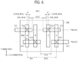
- FIG. 6 is a conceptual diagram of the layout of a first standard cell from which routing interference between internal pins has been removed according to the conditions illustrated in FIG. 3 ;
- FIG. 7 is a conceptual diagram of the layout of a second standard cell from which routing interference between internal pins and external pins is not removed according to the conditions illustrated in FIG. 3 ;
- FIG. 8 is a conceptual diagram of the layout of a first standard cell from which routing interference between internal pins and external pins has been removed according to the conditions illustrated in FIG. 3 ;
- FIG. 9 is a diagram of the layout of an AND-OR-inverter (AOI)22 cell corresponding to a first standard cell from which routing interference between internal pins has been removed;
- AOI AND-OR-inverter
- FIG. 10 is a diagram of the layout of an AOI22 cell corresponding to a first standard cell from which routing interference between internal pins and external pins has been removed;
- FIG. 11 is a block diagram of a design system which designs an integrated circuit including a first standard cell and a second standard cell according to some example embodiments of the inventive concepts;
- FIG. 12 is a flowchart of a method of laying out a first standard cell and a second standard cell according to some example embodiments of the inventive concepts.
- FIG. 13 is a flowchart of a method of laying out a first standard cell and a second standard cell according to other example embodiments of the inventive concepts.
- standard cell methodology is a method of designing application specific integrated circuits (ASICs) having normal digital-logic characteristics.
- a standard cell may refer to a group of transistors providing a Boolean logic function and/or a storage function (e.g., the function of a flip-flop or a latch) and interconnect structures.
- the Boolean logic function may be implemented as a tri-state logic circuit, an XOR gate, an XNOR gate, an AND gate, an OR gate, an inverter, a NAND gate, a NOR gate, an AND-OR-inverter (AOI) gate, or an OR-AND-inverter (OAI) gate, but example embodiments of the inventive concepts are not restricted to these examples.
- the Boolean logic function may refer to a first standard cell or a second standard cell which will be described below.
- routing interference exists between an A-pin (or A-metal) included in a lower metal layer and a B-pin (or a B-metal) included in an upper metal layer
- the routing of the A-pin may be considered when the B-pin is routed.
- routing interference does not exist between the A-pin and the B-pin, then the B-pin may be routed regardless of the routing of the A-pin.
- Existence of routing interference means that design rule check (DRC) violation is highly likely to occur.
- FIG. 1 is a conceptual diagram of a printed circuit board (PCB) including metal layers and vias.
- PCB printed circuit board
- the PCB 1000 is a PCB included in an integrated circuit (IC).
- the PCB 1000 may include a plurality of metal layers M 1 , M 2 , and M 3 , first vias VIA 1 electrically connecting the first metal layer M 1 and the second metal layers M 2 , and second vias VIA 2 electrically connecting the second metal layer M 2 and the third metal layers M 3 .
- first vias VIA 1 electrically connecting the first metal layer M 1 and the second metal layers M 2
- second vias VIA 2 electrically connecting the second metal layer M 2 and the third metal layers M 3 .
- the first metal layer M 1 is a lower metal layer and the second metal layer M 2 is an upper metal layer placed on or above the first metal layer M 1 . At least one metal layer may be placed between the first metal layer M 1 and the second metal layer M 2 .
- Each via VIA 2 illustrated in FIG. 1 connects a pin placed at the second metal layer M 2 with a pin placed at the third metal layer M 3 .
- FIGS. 2A and 2B are conceptual diagrams for explaining an unfolded transistor structure and a folded transistor structure.
- transistor folding is a technique for conserving a semiconductor area.
- the transistor folding is a process of transforming a single transistor into smaller and multiple transistors called folds, fingers, or legs, as shown in FIG. 2B .
- the folds, fingers, or legs are connected in parallel and need to be placed together on one semiconductor chip.
- Transistors are folded to meet a maximum height requirement.
- FIG. 2A shows a layout view LV 1 and a netlist view NV 1 of an inverter including transistors before folding.
- FIG. 2B shows a layout view LV 2 and a netlist view NV 2 of an inverter including transistors after folding.
- reference characters 51 and S 2 denote source regions
- reference characters D 1 and D 2 denote drain regions
- a reference character G denotes a gate electrode
- a reference character W 1 denotes the height of a P-row or P-channel metal oxide semiconductor (PMOS) transistor
- a reference character W 2 denotes the height of an N-row or N-channel metal oxide semiconductor (NMOS) transistor
- a reference character W 3 denotes the height of PMOS transistors having a folded structure.
- the schematic view NV 2 is equivalent to the schematic view NV 1 .
- FIG. 3 is a flowchart for explaining generation conditions for a first standard cell and generation conditions for a second standard cell.
- an IC design system 150 may determine whether a via center-to-via center space DV between a first via and a second via is greater than the double of a minimum metal center-to-metal center pitch DM between a first metal and a second metal.
- the center-to-via center space DV generically indicates DV 1 in FIG. 5 , DV 2 in FIG. 6 , DV 3 in FIG. 7 , and DV 4 in FIG. 8 .
- the IC design system 150 may determine whether all transistors included in a standard cell are unfolded transistors.
- the IC design system 150 may determine whether routing congestion is expected in the standard cell to be placed and routed.
- the IC design system 150 may place and route the standard cell as a first standard cell.
- the placement and routing of the first standard cell will be described with reference to FIGS. 6, 8, 9, and 10 later.
- the first standard cell may be a DRC clean standard cell or DRC violation-free standard cell.
- a tip-to-tip space in the first standard cell is designed to be equal to or greater than a DRC space. The tip-to-tip space and the DRC space will be described in detail with reference to FIGS. 5 through 8 later.
- the IC design system 150 may place and route the standard cell as a second standard cell.
- the placement and routing of the second standard cell will be described with reference to FIGS. 5 and 7 later.
- the second standard cell may be a DRC violation standard cell.
- a tip-to-tip space in the second standard cell is designed to be less than the DRC space.
- the IC design system 150 may not place and route a first standard cell and a second standard cell.
- Operation S 10 through S 50 may be performed by the IC design system 150 illustrated FIG. 11 .
- Operations S 10 through S 50 may be performed by a placement and routing tool 190 run in the IC design system 150 .
- FIG. 4 is a diagram of an IC 1000 A including both first and second standard cells.
- the IC 1000 A or the PCB 1000 A includes both a first standard cell 100 , 200 , 300 , or 400 and a second standard cell 10 or 50 .
- both the first standard cell 100 , 200 , 300 , or 400 and the second standard cell 10 or 50 are integrated together into the IC 1000 A. All transistors integrated into each standard cell 10 , 50 , 100 , 200 , 300 , or 400 are unfolded transistors as shown in FIG. 2A .
- the IC 1000 A includes a layout area into which the first standard cell 100 , 200 , 300 , or 400 and the second standard cell 10 or 50 can be integrated.
- Each of the unfolded transistors included in the first standard cell 100 , 200 , 300 , or 400 and the second standard cell 10 or 50 may be fabricated using sub-20 nm fin field effect transistor (FinFET) technology.
- FinFET fin field effect transistor
- FIGS. 5 to 10 illustrate conceptual diagrams of the layouts of a standard cell.
- an M 1 pin is a pin that is placed or routed on the first metal layer M 1 illustrated in FIG. 1
- an M 2 pin is a pin that is placed or routed on the second metal layer M 2 illustrated in FIG. 1 .
- Each via of vias V 1 through V 8 , V 11 through V 14 , V 21 through V 24 , 343 , 347 , 351 , 355 , 425 , 429 , and 457 is a first via VIA 1 which connects a pin placed on the first metal layer M 1 with a pin placed on the second metal layer M 2 in FIG. 1 .
- a pin may be a metal or a metal body.
- the first metal layer M 1 is a lower metal layer and the second metal layer M 2 is an upper metal layer placed on or above the first metal layer M 1 . At least one metal layer may be placed between the first metal layer M 1 and the second metal layer M 2 .
- Each via VIA 2 illustrated in FIG. 1 connects a pin placed at the second metal layer M 2 with a pin placed at the third metal layer M 3 .
- FIG. 5 is a conceptual diagram of the layout of the second standard cell 10 from which routing interference between internal pins is not removed according to the conditions illustrated in FIG. 3 .
- the IC design system 150 may place and route the second standard cell 10 . It is assumed that all transistors included in the second standard cell 10 are unfolded transistors.
- the second standard cell 10 includes M 1 pins A, B, C, and D; M 2 pins 21 , 25 , 31 , and 35 ; and the vias V 1 , V 2 , V 3 , and V 4 .
- the M 1 pins A, B, C, and D placed in a first direction (e.g., a Y-direction) successively side by side, are pins placed at the first metal layer M 1 .
- the M 2 pins 21 , 25 , 31 , and 35 placed in a second direction (e.g., an X-direction) are pins placed at the second metal layer M 2 .
- the first direction and the second direction are perpendicular to each other.
- the first direction or the Y-direction and the second direction or the X-direction illustrated in FIGS. 5 through 8 are illustrated to distinguish the placement directions of the pins A through D and 21 , 25 , 31 , and 35 .
- the first via V 1 is vertically connected between a first pin A and a fifth pin 21 .
- the second via V 2 is vertically connected between a third pin C and a sixth pin 25 .
- the third via V 3 is vertically connected between a second pin B and a seventh pin 31 .
- the fourth via V 4 is vertically connected between a fourth pin D and a eighth pin 35 .
- a via center-to-via center space DV 1 between the first via V 1 and the second via V 2 is greater than the double of the minimum metal center-to-metal center pitch DM between the first pin A and the second pin B. Accordingly, operation S 10 illustrated in FIG. 3 is satisfied. Since all transistors included in the second standard cell 10 are unfolded transistors, the IC design system 150 may determine that operation S 20 illustrated in FIG. 3 is satisfied.
- a tip-to-tip space T 2 T 1 defined by a distance between the fifth pin 21 and the sixth pin 25 placed at a first track TRACK 1 is less than a DRC space, i.e., a minimum spacing distance for DRC clean defined in design rules.
- the DRC space may be determined depending on a process. In other words, when the routing congestion is not expected in a standard cell to be placed and routed (i.e., in case of NO) in operation S 30 , the IC design system 150 may place and route the second standard cell 10 as the standard cell in the IC 1000 A.
- the via center-to-via center space DV 1 between the third via V 3 and the fourth via V 4 is greater than the double of the minimum metal center-to-metal center pitch DM between the first pin A and the second pin B.
- the tip-to-tip space T 2 T 1 defined by a distance between the seventh pin 31 and the eighth pin 35 placed at a second track TRACK 2 is less than the DRC space.
- a reference character MW denotes the width of each of the M 1 pins A, B, C, and D.
- a first overlap width OVL_W 1 a is an overlap width between the first pin A and the fifth pin 21 .
- a second overlap width OVL_W 2 a is the overlap width between the third pin C and the sixth pin 25 .
- a first via width VIA_W 1 a is the width of the first via V 1 and a second via width VIA_W 2 a is the width of the second via V 2 .
- the overlap widths OVL_W 1 a and OVL_W 2 a indicate minimum widths or areas which can secure the formation of the vias V 1 and V 2 , respectively.
- the M 1 pins A, B, C, and D have the same width MW.
- the first overlap width OVL_W 1 a is the same as the second overlap width OVL_W 2 a .
- the vias V 1 through V 4 have the same width.
- being the same means physically being the same and being the same in error range allowed during semiconductor manufacturing processes as well.
- the minimum metal center-to-metal center pitch DM in the second standard cell 10 is equal to or less than 80 nm, i.e., DM ⁇ 80 nm.
- a ratio of the first overlap width OVL_W 1 a to the width MW of the first pin A, i.e., OVL_W 1 a /MW may be equal to or greater than 0.8.
- FIG. 6 is a conceptual diagram of the layout of the first standard cell 100 from which routing interference between internal pins has been removed according to the conditions illustrated in FIG. 3 .
- the first standard cell 100 when the routing congestion is expected (i.e., in case of YES) in operation S 30 , the first standard cell 100 may be placed and routed. Referring to FIGS. 1 through 4 and FIG. 6 , it is assumed that all transistors included in the first standard cell 100 are unfolded transistors.
- the first standard cell 100 includes the M 1 pins A, B, C, and D; M 2 pins 121 , 123 , 125 , and 127 ; and the vias V 11 , V 12 , V 13 , and V 14 .
- the M 1 pins A, B, C, and D, placed in the first direction successively side by side, are pins placed at the first metal layer M 1 .
- the M 2 pins 121 , 123 , 125 , and 127 placed in the second direction are pins placed at the second metal layer M 2 .
- the first via V 11 is vertically connected between the first pin A and the fifth pin 121 .
- the second via V 12 is vertically connected between the third pin C and the sixth pin 123 .
- the third via V 13 is vertically connected between the second pin A and the seventh pin 125 .
- the fourth via V 14 is vertically connected between the fourth pin D and the eighth pin 127 .
- a via center-to-via center space DV 2 between the first via V 11 and the second via V 12 is greater than the double of the minimum metal center-to-metal center pitch DM between the first pin A and the second pin B. Accordingly, the IC design system 150 may determine that operation S 10 illustrated in FIG. 3 is satisfied. Since all transistors included in the first standard cell 100 are unfolded transistors, the IC design system 150 may determine that operation S 20 illustrated in FIG. 3 is satisfied.
- a tip-to-tip space T 2 T 2 defined by a distance between the fifth pin 121 and the sixth pin 123 placed at the first track TRACK 1 is equal to or greater than the DRC space, i.e., the minimum spacing distance for DRC clean defined in design rules.
- the IC design system 150 may place and route the first standard cell 100 as the standard cell in the IC 1000 A.
- the via center-to-via center space DV 2 between the third via V 13 and the fourth via V 14 is greater than the double of the minimum metal center-to-metal center pitch DM between the first pin A and the second pin B.
- the tip-to-tip space T 2 T 2 defined by a distance between the seventh pin 125 and the eighth pin 127 placed at a second track TRACK 2 is equal to or greater than the DRC space.
- the reference character MW denotes the width of each of the M 1 pins A, B, C, and D.
- a first overlap width OVL_W 1 b is the overlap width between the first pin A and the fifth pin 121 .
- a second overlap width OVL_W 2 b is the overlap width between the third pin C and the sixth pin 123 .
- a first via width VIA_W 1 b is the width of the first via V 11 and a second via width VIA_W 2 b is the width of the second via V 12 .
- the M 1 pins A, B, C, and D have the same width MW.
- the first overlap width OVL_W 1 b is the same as the second overlap width OVL_W 2 b .
- the vias V 11 through V 14 have the same width.
- the minimum metal center-to-metal center pitch DM in the first standard cell 100 is equal to or less than 80 nm.
- a ratio of the first overlap width OVL_W 1 b to the width MW of the first pin A, i.e., OVL_W 1 b /MW may be equal to or greater than 0.8.
- routing interference exists between the first and second pins A and B, between the first and third pins A and C, between the fourth and third pins D and C, and between the fourth and second pins D and B in the second standard cell 10 .
- the first overlap width OVL_W 1 b may influence the routing of the third pin C as well as the second pin B.
- a distance between the first and third pins A and C in the first standard cell 100 illustrated in FIG. 6 is greater than a distance between the first and third pins A and C in the second standard cell 10 illustrated in FIG. 5 .
- the tip-to-tip space T 2 T 2 is greater than the tip-to-tip space T 2 T 1
- the via center-to-via center space DV 2 is greater than the via center-to-via center space DV 1 .
- routing interference exists between the first and second pins A and B but does not exist between the first and third pins A and C.
- routing interference exists between the fourth and third pins D and C but does not exist between the fourth and second pins D and B.
- routing interference between the first and third pins A and C and between the fourth and second pins D and B is eliminated.
- FIG. 7 is a conceptual diagram of the layout of the second standard cell 50 from which routing interference between internal pins and external pins is not removed according to the conditions illustrated in FIG. 3 .
- M 1 pins E, F, G, and H, M 2 pins 59 and 77 , and vias V 5 and V 8 are placed and routed inside the second standard cell 50 ; and M 1 pins I and J, M 2 pins 65 and 73 , and vias V 6 and V 7 are placed and routed outside the second standard cell 50 .
- the IC design system 150 may place and route the second standard cell 50 . It is assumed that all transistors included in the second standard cell 50 are unfolded transistors.
- the first via V 7 is vertically connected between the first pin I and the ninth pin 73 .
- the second via V 8 is vertically connected between the third pin F and the tenth pin 77 .
- the third via V 5 is vertically connected between the fourth pin G and the seventh pin 59 .
- the fourth via V 6 is vertically connected between the sixth pin J and the eighth pin 65 .
- a via center-to-via center space DV 3 between the first via V 7 and the second via V 8 is greater than the double of the minimum metal center-to-metal center pitch DM between the second pin E and the third pin F. Accordingly, the IC design system 150 may determine that operation S 10 illustrated in FIG. 3 is satisfied. Since all transistors included in the second standard cell 50 are unfolded transistors, the IC design system 150 may determine that operation S 20 illustrated in FIG. 3 is satisfied.
- a tip-to-tip space T 2 T 3 defined by a distance between the ninth pin 73 and the tenth pin 77 placed at the second track TRACK 2 is less than the DRC space, i.e., the minimum spacing distance for DRC clean defined in design rules.
- the IC design system 150 may place and route the second standard cell 50 as the standard cell in the IC 1000 A.
- the via center-to-via center space DV 3 between the third via V 5 and the fourth via V 6 is greater than the double of the minimum metal center-to-metal center pitch DM between the second pin E and the third pin F.
- the tip-to-tip space T 2 T 3 defined by a distance between the seventh pin 59 and the eighth pin 65 placed at the first track TRACK 1 is less than the DRC space.
- the reference character MW denotes the width of each of the M 1 pins I, E, F, G, H, and J.
- a first overlap width OVL_W 1 c is the overlap width between the first pin I and the ninth pin 73 .
- a second overlap width OVL_W 2 c is the overlap width between the third pin F and the tenth pin 77 .
- a first via width VIA_W 1 c is the width of the first via V 7 and a second via width VIA_W 2 c is the width of the second via V 8 .
- the M 1 pins I, E, F, G, H, and J have the same width MW.
- the first overlap width OVL_W 1 c is the same as the second overlap width OVL_W 2 c .
- the vias V 5 through V 8 have the same width.
- the minimum metal center-to-metal center pitch DM in the first standard cell 100 is equal to or less than 80 nm.
- a ratio of the first overlap width OVL_W 1 c to the width MW of the first pin I, i.e., OVL_W 1 c /MW may be equal to or greater than 0.8.
- FIG. 8 is a conceptual diagram of the layout of the first standard cell 200 from which routing interference between internal pins and external pins has been removed according to the conditions illustrated in FIG. 3 .
- the M 1 pins E, F, G, and H, M 2 pins 231 and 237 , and vias V 21 and V 24 are placed and routed inside the first standard cell 200 ; and the M 1 pins I and J, M 2 pins 233 and 235 , and vias V 23 and V 22 are placed and routed outside the first standard cell 200 .
- the IC design system 150 may place and route the first standard cell 200 . It is assumed that all transistors included in the first standard cell 200 are unfolded transistors.
- the first via V 23 is vertically connected between the first pin I and the ninth pin 235 .
- the second via V 24 is vertically connected between the third pin F and the tenth pin 237 .
- the third via V 21 is vertically connected between the fourth pin G and the seventh pin 231 .
- the fourth via V 22 is vertically connected between the sixth pin J and the eighth pin 233 .
- a via center-to-via center space DV 4 between the first via V 23 and the second via V 24 is greater than the double of the minimum metal center-to-metal center pitch DM between the second pin E and the third pin F. Accordingly, the IC design system 150 may determine that operation S 10 illustrated in FIG. 3 is satisfied. Since all transistors included in the first standard cell 200 are unfolded transistors, the IC design system 150 may determine that operation S 20 illustrated in FIG. 3 is satisfied.
- a tip-to-tip space T 2 T 4 defined by a distance between the ninth pin 235 and the tenth pin 237 placed at the second track TRACK 2 is equal to or greater than the DRC space, i.e., the minimum spacing distance for DRC clean defined in design rules.
- the IC design system 150 may place and route the first standard cell 200 as the standard cell in the IC 1000 A.
- the via center-to-via center space DV 4 between the third via V 21 and the fourth via V 22 is greater than the double of the minimum metal center-to-metal center pitch DM between the second pin E and the third pin F.
- the tip-to-tip space T 2 T 4 defined by a distance between the seventh pin 231 and the eighth pin 233 placed at the first track TRACK 1 is equal to or greater than the DRC space.
- the reference character MW denotes the width of each of the M 1 pins I, E, F, G, H, and J.
- a first overlap width OVL_W 1 d is the overlap width between the first pin I and the ninth pin 235 .
- a second overlap width OVL_W 2 d is the overlap width between the third pin F and the tenth pin 237 .
- a first via width VIA_W 1 d is the width of the first via V 23 and a second via width VIA_W 2 d is the width of the second via V 24 .
- the M 1 pins I, E, F, G, H, and J have the same width MW.
- the first overlap width OVL_W 1 d is the same as the second overlap width OVL_W 2 d .
- the vias V 21 through V 24 have the same width.
- the minimum metal center-to-metal center pitch DM in the first standard cell 200 is equal to or less than 80 nm.
- a ratio of the first overlap width OVL_W 1 d to the width MW of the first pin I, i.e., OVL_W 1 d /MW may be equal to or greater than 0.8.
- the via widths VIA_W 1 a , VIA_W 1 b , VIA_W 1 c , and VIA_W 1 d may be the same as one another; the via widths VIA_W 2 a , VIA_W 2 b , VIA_W 2 c , and VIA_W 2 d may be the same as one another; the overlap widths OVL_W 1 a , OVL_W 1 b , OVL_W 1 c , and OVL_W 1 d may be the same as one another; and the overlap widths OVL_W 2 a , OVL_W 2 b , OVL_W 2 c , and OVL_W 2 d may be the same as one another.
- routing interference exists between the first and second pins I and E, between the first and third pins I and F, between the sixth and fifth pins J and H, and between the sixth and fourth pins J and G in the second standard cell 50 .
- the first overlap width OVL_W 1 d may influence the routing of the third pin F as well as the second pin E.
- the distance between the first and third pins I and F in the first standard cell 200 illustrated in FIG. 8 is greater than the distance between the first and third pins I and F in the second standard cell 50 illustrated in FIG. 7 .
- the tip-to-tip space T 2 T 4 is greater than the tip-to-tip space T 2 T 3 , and therefore, the via center-to-via center distance DV 4 is greater than the via center-to-via center distance DV 3 .
- the routing interference still exists between the first and second pins I and E but does not exist between the first and third pins I and F.
- the routing interference still exists between the sixth and fifth pins J and H but does not exist between the sixth and fourth pins J and G.
- the routing interference is eliminated.
- the routing interference between the first and third pins I and F and between the sixth and fourth pins J and G is eliminated.
- the layout area of the first standard cell 200 illustrated in FIG. 8 is greater than the layout area of the second standard cell 50 illustrated in FIG. 7 , but routing efficiency increases when the first standard cell 200 is placed.
- FIG. 9 is a diagram of the layout of an AOI22 cell corresponding to a first standard cell from which routing interference between internal pins has been removed.
- the first standard cell 300 integrated into the IC 1000 A illustrated in FIG. 4 may be implemented as an AOI22 gate circuit.
- the AOI22 gate circuit 300 illustrated in FIG. 9 has a layout for eliminating or reducing routing interference among internal cell pins 323 , 325 , 327 , and 329 , which have been described with reference to FIG. 6 .
- the AOI22 gate circuit 300 includes five M 1 pins 323 , 325 , 327 , 329 , and 331 and four M 2 pins 341 , 345 , 349 , and 353 .
- the M 2 pins 341 and 349 are placed along the first M 2 track TRACK 1 and the M 2 pins 345 and 353 are placed along the second M 2 track TRACK 2 .
- a first via 343 is used to vertically connect the second pin 325 with the sixth pin 341
- a second via 351 is used to vertically connect the fourth pin 329 with the seventh pin 349
- a third via 355 is used to vertically connect the first pin 323 with the eighth pin 353
- a fourth via 347 is used to vertically connect the third pin 327 with the ninth pin 345 .
- a tip-to-tip space D 33 between the eighth pin 353 and the ninth pin 345 is greater than the DRC space.
- a tip-to-tip space D 31 between the sixth pin 341 and the seventh pin 349 is greater than the DRC space.
- the technical ideas about the placement and routing of the first standard cell 100 described with reference to FIG. 6 are applied to the placement and routing of the first standard cell 300 illustrated in FIG. 9 .
- FIG. 10 is a diagram of the layout of an AOI22 cell corresponding to a first standard cell from which routing interference between internal pins and external pins has been removed.
- an electronic circuit 400 including an AOI22 gate circuit 420 and an inverter 450 may be integrated into the IC 1000 A illustrated in FIG. 4 .
- the AOI22 gate circuit 420 may refer to the first standard cell 420 .
- the electronic circuit 400 has a layout for eliminating or reducing routing interference among internal pins 423 , 427 , 431 , 433 , and 435 inside the first standard cell 420 and external pins 451 and 453 outside the first standard cell 420 .
- the AOI22 gate circuit 420 includes five M 1 pins 423 , 427 , 431 , 433 , and 435 and two M 2 pins 437 and 439 .
- the M 2 pin 437 is placed along the first M 2 track TRACK 1 and the M 2 pin 439 is placed along the second M 2 track TRACK 2 .
- the inverter 450 includes the M 1 pins 451 and 453 , an M 2 pin 455 , and a via 457 .
- the M 2 pin 455 is placed along the second M 2 track TRACK 2 and the via 457 is used to vertically connect the M 1 pin 453 with the M 2 pin 455 .
- a tip-to-tip space D 41 between the M 2 pins 439 and 455 is greater than the DRC space.
- the distance between the pins 453 and 427 coming at first and third places starting from the first pin 453 among at least three pins 453 , 423 , 427 , 431 , 433 , and 435 placed successively side by side increases; routing interference between the pins 453 and 427 at the first and third places is eliminated.
- the technical ideas about the placement and routing of the first standard cell 200 described with reference to FIG. 8 are applied to the placement and routing of the first standard cell 420 illustrated in FIG. 10 .
- FIG. 11 is a block diagram of the design system 150 which designs an IC including a first standard cell and a second standard cell according to some example embodiments of the inventive concepts.
- the IC design system 150 may include a memory device 170 and a placement and routing tool 190 .
- the memory device 170 may include a non-transitory computer readable medium.
- non-transitory computer-readable media include magnetic media such as hard disks, floppy disks, and magnetic tape; optical media such as CD ROM discs and DVDs; magneto-optical media such as optical discs; and hardware devices that are specially configured to store and perform program instructions, such as read-only memory (ROM), random access memory (RAM), flash memory, and the like.
- the non-transitory computer-readable media may also be a distributed network, so that the program instructions are stored and executed in a distributed fashion.
- the memory device 170 may store a design file 171 , a first cell library 173 , and a second cell library 177 .
- the design file 171 may include information for a netlist and information for a standard cell layout.
- the first cell library 173 may store netlist information for the library of the first standard cells 100 and 200 which have been changed to eliminate routing interference between adjacent pins as described with reference to FIGS. 6 and 8 .
- the first cell library 173 may store information indicating one or more cell layouts 175 of each of the first standard cells 100 and 200 stored therein.
- the cell layouts 175 may store information indicating the position, size, orientation, and input/output (I/O) nets of each of the cell layouts 175 .
- the first cell library 173 may be referred to as a routing friendly library.
- the second cell library 177 may store netlist information for the library of the original second standard cells 10 and 50 which have been described with reference to FIGS. 5 and 7 .
- the second cell library 177 may store information indicating one or more cell layouts 179 of each of the second standard cells 10 and 50 stored therein.
- the cell layouts 179 may store information indicating the position, size, orientation, and I/O nets of each of the cell layouts 177 .
- the second cell library 177 may be referred to as an original standard cell library.
- the placement and routing tool 190 may include a central processing unit (CPU) or processor 191 and optionally a memory.
- CPU central processing unit
- processor 191 optionally a memory.
- the CPU 191 may include at least one processor implemented by at least one semiconductor chip disposed on a printed circuit board.
- the processor may be an arithmetic logic unit, a digital signal processor, a microcomputer, a field programmable array, a programmable logic unit, a microprocessor or any other device capable of responding to and executing instructions in a defined manner.
- the memory may contain computer readable code that, when executed by the processor, configures the CPU 191 as a special purpose computer. For example, when executed, the code may configure the CPU 191 to configure layouts of standard cells such as a first standard cell and a second standard cell, and to route connections between the layouts based on an input netlist.
- the placement and routing tool 190 may use the layouts of standard cell such as a first standard cell and a second standard cell determined by a determination logic 193 .
- the memory may include code that, when executed configures the CPU 191 to perform the functions of the determination logic 193 , such that the determination logic 193 may be implemented as a software component executed by a central processing unit (CPU) 191 .
- the determination logic 193 may be a hardware component such as a determination logic circuit.
- the determination logic 193 may estimate a region in which routing congestion will occur and a region in which routing congestion will not occur and determine which of the cell layouts 175 in the first cell library 173 and the cell layouts 179 in the second cell library 177 will be subjected to the placement and routing according to the estimation result.
- the region may refer to a region in which the first standard cell 100 , 200 , 300 , or 400 and/or the second standard cell 10 or 50 will be placed and routed.
- the determination logic 193 may use the cell layouts 179 in the second cell library 177 in initial placement and routing and may determine to replace the cell layouts 179 in the second cell library 177 with the cell layouts 175 in the first cell library 173 for a region having routing congestion.
- FIG. 12 is a flowchart of a method of laying out a first standard cell and a second standard cell according to some example embodiments of the inventive concepts.
- the placement and routing tool 190 may plan placement and routing.
- the placement and routing tool 190 may partition a placement and routing area into a plurality of regions.
- the placement and routing tool 190 may determine whether each of the regions is expected to have routing congestion or not. Routing congestion may be determined based on the number of DRC violations.
- the determination logic 193 may count the number of DRC violations occurring in a target region (i.e., a partitioned region) and compare a count value with a reference value. When the count value is equal to or greater than the reference value, the determination logic 193 may determine that the target region is expected to have routing congestion. When the count value is less than the reference value, the determination logic 193 may determine that the target region is not expected to have routing congestion.
- the DRC violation count value for each track in the standard cell 10 or 50 may be 2, but example embodiments of the inventive concepts are not restricted to these example embodiments. The count value of 2 is just an example.
- the reference value may be determined by a designer of the IC 1000 A.
- the placement and routing tool 190 may perform placement and routing on the region expected to have routing congestion using the cell layouts 175 in the first cell library 173 .
- a first standard cell may be placed and routed in the region expected to have routing congestion.
- Examples of the first standard cell may be the standard cells 100 , 200 , 300 , and 420 described with reference to FIGS. 6, 8, 9 , and 10 .
- the placement and routing tool 190 may perform placement and routing on the region which is expected to not have routing congestion (i.e., the region having the count value less than the reference value) using the cell layouts 179 in the second cell library 177 .
- a second standard cell may be placed and routed in the region expected to not have routing congestion. Examples of the second standard cell may be the standard cells 10 and 50 described with reference to FIGS. 5 and 7 .
- first standard cell 100 , 200 , 300 , or 420 and the second standard cell 10 or 50 are illustrated in FIG. 4
- at least one peripheral pin connected to the standard cell 50 , 200 , or 420 may be placed and routed in the IC 1000 A as shown in FIGS. 7, 8, and 10 .
- the first standard cell 420 may be placed and routed together with the inverter 450 in the IC 1000 A, as shown in FIG. 10 .
- FIG. 13 is a flowchart of a method of laying out a first standard cell and a second standard cell according to other example embodiments of the inventive concepts.
- the placement and routing tool 190 may perform initial placement and routing using the cell layouts 179 in the second cell library 177 .
- the placement and routing tool 190 may search for or determine regions having routing congestion among region subjected to the placement and routing.
- Operation S 220 of FIG. 13 may be performed in a similar manner to operation S 130 of FIG. 12 .
- the placement and routing tool 190 and more particularly, the determination logic 193 may count the number of DRC violations in each of the region subjected to the placement and routing, compare a count value corresponding to the number of DRC violations with a reference value, and determine the region for which the count value is equal to or greater than the reference value as having routing congestion.
- the placement and routing tool 190 may replace (or substitute) cell layouts that have been placed and routed in the regions with the cell layouts 175 in the first cell library 173 . Since the replaced standard cell (or the layout of a first standard cell) may be larger than an original standard cell (or the layout of a second standard cell), a DRC violation may occur when the standard cell is replaced only causing an overlapping between the replaced standard cell and an adjacent standard cell.
- the placement and routing tool 190 performs placement on the adjacent standard cell after performing the replacement.
- the placement and routing tool 190 may perform placement and routing adjustment by removing the overlap area between the standard cells and newly perform routing to eliminate the DRC violation.
- the placement and routing tool 190 may estimate the shape or structure of vias and/or M 2 pins which are connected to M 1 pins and may restructure a standard cell layout and replace the M 1 pins and the M 2 pins according to the estimation result. Accordingly, the placement and routing tool 190 minimizes routing interference between the M 1 pins and the M 2 pins, so that routing efficiency is increased while a block level area is decreased.
- the block level area may be an area occupied by standard cells in the entire area of an IC.
- the area of the standard cell layout may increase.
- the placement and routing tool 190 may place a standard cell, which has a small layout area, at a region having low routing congestion and place a standard cell, which is advantageous to routing even through having a large layout area, at a region having high routing congestion. Through such operation, the overall block level area is decreased.
- the placement and routing tool 190 may reduce (or, alternatively, overcome) the difficulties or problems which may occur during placement and routing due to the miniaturization or shrinkage of manufacturing processes.
- a standard cell i.e., the first standard cell and/or the second standard cell
- a standard cell layout i.e., a first standard cell layout and/or a second standard cell layout
- FIGS. 4 through 10 may be formed in an IC.
- the IC 1000 A illustrated in FIG. 4 may be a CPU, a processor, an application processor, or a digital signal processor but is not restricted thereto.
- the IC 1000 A illustrated in FIG. 4 may be used in various electronic devices or systems.
- a placement and routing area is partitioned into a plurality of areas in operation S 120 .
- the placement and routing tool 190 determines whether each partitioned region has routing congestion based on the number of DRC violations in operation S 130 .
- the determination logic 193 may count the number of DRC violations occurring in a target region (i.e., a partitioned region) and compare a count value with a reference value. When the count value is equal to or greater than the reference value, the placement and routing tool 190 may determine that the target region has routing congestion. When the count value is less than the reference value, the placement and routing tool 190 may determine that the target region does not have routing congestion.
- the placement and routing tool 190 places and routes a first standard cell in the partitioned region determined as having routing congestion using a cell layout in a first cell library in operations S 140 and S 160 . However, the placement and routing tool 190 places and routes a second standard cell in the partitioned region determined as not having routing congestion using a cell layout in a second cell library in operations S 150 and S 160 .
- the placement and routing tool 190 places and routes the first standard cell 100 in the IC 1000 A.
- the placement and routing tool 190 formed only first unfolded transistors in the first standard cell 100 ; places, successively side by side, the first, second and third metals A, B, and C in the first direction at the first layer M 1 ; places the fourth metal 121 and the fifth metal 123 separated from each other and in the second direction at the second layer M 2 ; connects the first metal A with the fourth metal 121 using the first via V 11 , and connects the third metal C with the fifth metal 123 using the second via V 12 .
- the via center-to-via center space DV 2 between the first via V 11 and the second via V 12 is greater than the double of the minimum metal center-to-metal center pitch DM between the first metal A and the second metal B.
- the minimum metal center-to-metal center pitch DM is equal to or less than 80 nm.
- the tip-to-tip space T 2 T 2 between the fourth metal 121 and the fifth metal 123 is equal to or greater than the minimum spacing distance for DRC clean.
- the placement and routing tool 190 places and routes the second standard cell 10 in the IC 1000 A.
- the placement and routing tool 190 formed only second unfolded transistors in the second standard cell 10 ; places, successively side by side, the sixth, seventh and eighth metals A, B, and C in the first direction at the first layer M 1 ; places the ninth metal 21 and the tenth metal 25 separated from each other in the second direction at the second layer M 2 ; connects the sixth metal A with the ninth metal 21 using the third via V 1 , and connects the eighth metal C with the tenth metal 25 using the fourth via V 2 .
- the via center-to-via center space DV 1 between the third via V 11 and the fourth via V 12 is greater than the double of the minimum metal center-to-metal center pitch DM between the sixth metal A and the seventh metal B.
- the minimum metal center-to-metal center pitch DM is equal to or less than 80 nm.
- the tip-to-tip space T 2 T 1 between the ninth metal 21 and the tenth metal 25 is less than the minimum spacing distance for DRC clean.
- a standard cell or a standard cell layout increases a space between the first and third pins among at least three pins placed side by side, thereby eliminating routing interference between the first and third pins. Since the standard cell layout eliminates or reduces routing interference between pins among at least three pins placed side by side, the routing efficiency of the standard cell is increased.
- the standard cell is routed using different standard cell libraries according to whether the standard cell has routing congestion or not, so that an overall block level area is decreased.
Landscapes
- Physics & Mathematics (AREA)
- Mathematical Physics (AREA)
- Engineering & Computer Science (AREA)
- General Engineering & Computer Science (AREA)
- Computer Hardware Design (AREA)
- Computing Systems (AREA)
- Computer Networks & Wireless Communication (AREA)
- Design And Manufacture Of Integrated Circuits (AREA)
- Geometry (AREA)
Abstract
Description
DV1=½VIA_W1a+OVL_W1a+T2T1+OVL_W2a+½VIA_W2a. (1)
DV1=½VIA_W1a*2+OVL_W1a*2+T2T1. (2)
DV2=½VIA_W1b*2+OVL_W1b*2+T2T2. (3)
DV3=½VIA_W1c*2+OVL_W1c*2+T2T3. (4)
DV4=½VIA_W1d*2+OVL_W1d*2+T2T4. (5)
Claims (12)
Priority Applications (1)
| Application Number | Priority Date | Filing Date | Title |
|---|---|---|---|
| US16/725,023 US11031385B2 (en) | 2016-04-07 | 2019-12-23 | Standard cell for removing routing interference between adjacent pins and device including the same |
Applications Claiming Priority (4)
| Application Number | Priority Date | Filing Date | Title |
|---|---|---|---|
| KR1020160042588A KR102504289B1 (en) | 2016-04-07 | 2016-04-07 | Standard cell configured to remove routing interference between adjacent pins |
| KR10-2016-0042588 | 2016-04-07 | ||
| US15/298,586 US10553574B2 (en) | 2016-04-07 | 2016-10-20 | Standard cell for removing routing interference between adjacent pins and device including the same |
| US16/725,023 US11031385B2 (en) | 2016-04-07 | 2019-12-23 | Standard cell for removing routing interference between adjacent pins and device including the same |
Related Parent Applications (1)
| Application Number | Title | Priority Date | Filing Date |
|---|---|---|---|
| US15/298,586 Continuation US10553574B2 (en) | 2016-04-07 | 2016-10-20 | Standard cell for removing routing interference between adjacent pins and device including the same |
Publications (2)
| Publication Number | Publication Date |
|---|---|
| US20200126968A1 US20200126968A1 (en) | 2020-04-23 |
| US11031385B2 true US11031385B2 (en) | 2021-06-08 |
Family
ID=59998325
Family Applications (2)
| Application Number | Title | Priority Date | Filing Date |
|---|---|---|---|
| US15/298,586 Active 2038-02-27 US10553574B2 (en) | 2016-04-07 | 2016-10-20 | Standard cell for removing routing interference between adjacent pins and device including the same |
| US16/725,023 Active US11031385B2 (en) | 2016-04-07 | 2019-12-23 | Standard cell for removing routing interference between adjacent pins and device including the same |
Family Applications Before (1)
| Application Number | Title | Priority Date | Filing Date |
|---|---|---|---|
| US15/298,586 Active 2038-02-27 US10553574B2 (en) | 2016-04-07 | 2016-10-20 | Standard cell for removing routing interference between adjacent pins and device including the same |
Country Status (2)
| Country | Link |
|---|---|
| US (2) | US10553574B2 (en) |
| KR (1) | KR102504289B1 (en) |
Families Citing this family (15)
| Publication number | Priority date | Publication date | Assignee | Title |
|---|---|---|---|---|
| KR102504289B1 (en) * | 2016-04-07 | 2023-02-28 | 삼성전자 주식회사 | Standard cell configured to remove routing interference between adjacent pins |
| US9977854B2 (en) * | 2016-07-12 | 2018-05-22 | Ati Technologies Ulc | Integrated circuit implementing standard cells with metal layer segments extending out of cell boundary |
| US10642949B2 (en) * | 2017-06-07 | 2020-05-05 | Taiwan Semiconductor Manufacturing Co., Ltd. | Cell placement site optimization |
| US10741539B2 (en) | 2017-08-30 | 2020-08-11 | Taiwan Semiconductor Manufacturing Co., Ltd. | Standard cells and variations thereof within a standard cell library |
| DE102017127276A1 (en) | 2017-08-30 | 2019-02-28 | Taiwan Semiconductor Manufacturing Co., Ltd. | STANDARD CELLS AND ADAPTATIONS FROM THEREOF WITHIN A STANDARD CELL LIBRARY |
| KR102387946B1 (en) | 2018-05-21 | 2022-04-18 | 삼성전자주식회사 | Integrated Circuit Including Clubfoot Structure Conductive Patterns |
| US11030372B2 (en) | 2018-10-31 | 2021-06-08 | Taiwan Semiconductor Manufacturing Company Ltd. | Method for generating layout diagram including cell having pin patterns and semiconductor device based on same |
| CN109558667B (en) * | 2018-11-23 | 2023-07-14 | 珠海一微半导体股份有限公司 | An Optimization Method Based on Routing Blocking |
| US11387229B2 (en) | 2019-06-14 | 2022-07-12 | Samsung Electronics Co., Ltd. | Semiconductor device |
| US11495540B2 (en) | 2019-10-22 | 2022-11-08 | Tokyo Electron Limited | Semiconductor apparatus having stacked devices and method of manufacture thereof |
| KR102918411B1 (en) * | 2021-03-12 | 2026-01-26 | 삼성전자주식회사 | Semiconductor device |
| US12100660B2 (en) * | 2021-10-04 | 2024-09-24 | Advanced Micro Devices, Inc. | Low congestion standard cells |
| CN114861587B (en) * | 2022-04-07 | 2023-03-10 | 珠海妙存科技有限公司 | A method, system, device, and storage medium for designing chip carrier board pin layout |
| CN115909899B (en) * | 2022-11-21 | 2026-02-24 | 福州京东方光电科技有限公司 | Display panel, circuit board and display device |
| JP2024083870A (en) * | 2022-12-12 | 2024-06-24 | キオクシア株式会社 | Semiconductor integrated circuit, layout design system, layout design method, and program |
Citations (19)
| Publication number | Priority date | Publication date | Assignee | Title |
|---|---|---|---|---|
| US5980093A (en) | 1996-12-04 | 1999-11-09 | Lsi Logic Corporation | Integrated circuit layout routing using multiprocessing |
| US20060117276A1 (en) * | 2004-11-29 | 2006-06-01 | Fujitsu Limited | Semiconductor integrated circuit designing method and program |
| US20070022400A1 (en) | 2005-07-19 | 2007-01-25 | Matsushita Electric Industrial Co., Ltd. | Method, program, and apparatus for designing layout of semiconductor integrated circuit |
| US20090172628A1 (en) | 2007-12-26 | 2009-07-02 | Cadence Design Systems, Inc. | Method and System for Utilizing Hard and Preferred Rules for C-Routing of Electronic Designs |
| US7971174B1 (en) | 2008-09-18 | 2011-06-28 | Cadence Design Systems, Inc. | Congestion aware pin optimizer |
| US8065652B1 (en) | 2007-08-13 | 2011-11-22 | Cadence Design Systems, Inc. | Method and system for determining hard and preferred rules in global routing of electronic designs |
| US8127263B2 (en) | 2009-02-03 | 2012-02-28 | Texas Instruments Incorporated | Improving routability of integrated circuit design without impacting the design area |
| US8173491B2 (en) | 2008-12-18 | 2012-05-08 | Taiwan Semiconductor Manufacturing Co., Ltd. | Standard cell architecture and methods with variable design rules |
| US20130072020A1 (en) * | 2011-09-19 | 2013-03-21 | Texas Instruments Incorporated | Method For Ensuring DPT Compliance for Auto-Routed Via Layers |
| US20130227498A1 (en) * | 2012-02-27 | 2013-08-29 | Globalfoundries Inc. | Pattern based method for identifying design for manufacturing improvement in a semiconductor device |
| US20130272056A1 (en) * | 2012-04-13 | 2013-10-17 | Taiwan Semicconductor Manufacturing Company, Ltd. | Apparatus for SRAM Cells |
| US20140027783A1 (en) * | 2012-07-25 | 2014-01-30 | Huaxiang Yin | Semiconductor device and method of manufacturing the same |
| US20140038085A1 (en) * | 2012-07-31 | 2014-02-06 | Taiwan Semiconductor Manufacturing Co., Ltd. | Automatic Misalignment Balancing Scheme for Multi-Patterning Technology |
| US8735857B2 (en) | 2010-12-22 | 2014-05-27 | Easic Corporation | Via-configurable high-performance logic block architecture |
| US8904335B2 (en) | 2013-03-25 | 2014-12-02 | GlobalFoundries, Inc. | Evaluation of pin geometry accessibility in a layer of circuit |
| US8978004B2 (en) | 2012-02-10 | 2015-03-10 | Freescale Semiconductor, Inc. | Cell routability prioritization |
| US9122830B2 (en) | 2013-06-03 | 2015-09-01 | Globalfoundries Inc. | Wide pin for improved circuit routing |
| US20160117432A1 (en) * | 2014-10-24 | 2016-04-28 | Globalfoundries Inc. | Method and apparatus for assisted metal routing |
| US10553574B2 (en) * | 2016-04-07 | 2020-02-04 | Samsung Electronics Co., Ltd. | Standard cell for removing routing interference between adjacent pins and device including the same |
-
2016
- 2016-04-07 KR KR1020160042588A patent/KR102504289B1/en active Active
- 2016-10-20 US US15/298,586 patent/US10553574B2/en active Active
-
2019
- 2019-12-23 US US16/725,023 patent/US11031385B2/en active Active
Patent Citations (19)
| Publication number | Priority date | Publication date | Assignee | Title |
|---|---|---|---|---|
| US5980093A (en) | 1996-12-04 | 1999-11-09 | Lsi Logic Corporation | Integrated circuit layout routing using multiprocessing |
| US20060117276A1 (en) * | 2004-11-29 | 2006-06-01 | Fujitsu Limited | Semiconductor integrated circuit designing method and program |
| US20070022400A1 (en) | 2005-07-19 | 2007-01-25 | Matsushita Electric Industrial Co., Ltd. | Method, program, and apparatus for designing layout of semiconductor integrated circuit |
| US8065652B1 (en) | 2007-08-13 | 2011-11-22 | Cadence Design Systems, Inc. | Method and system for determining hard and preferred rules in global routing of electronic designs |
| US20090172628A1 (en) | 2007-12-26 | 2009-07-02 | Cadence Design Systems, Inc. | Method and System for Utilizing Hard and Preferred Rules for C-Routing of Electronic Designs |
| US7971174B1 (en) | 2008-09-18 | 2011-06-28 | Cadence Design Systems, Inc. | Congestion aware pin optimizer |
| US8173491B2 (en) | 2008-12-18 | 2012-05-08 | Taiwan Semiconductor Manufacturing Co., Ltd. | Standard cell architecture and methods with variable design rules |
| US8127263B2 (en) | 2009-02-03 | 2012-02-28 | Texas Instruments Incorporated | Improving routability of integrated circuit design without impacting the design area |
| US8735857B2 (en) | 2010-12-22 | 2014-05-27 | Easic Corporation | Via-configurable high-performance logic block architecture |
| US20130072020A1 (en) * | 2011-09-19 | 2013-03-21 | Texas Instruments Incorporated | Method For Ensuring DPT Compliance for Auto-Routed Via Layers |
| US8978004B2 (en) | 2012-02-10 | 2015-03-10 | Freescale Semiconductor, Inc. | Cell routability prioritization |
| US20130227498A1 (en) * | 2012-02-27 | 2013-08-29 | Globalfoundries Inc. | Pattern based method for identifying design for manufacturing improvement in a semiconductor device |
| US20130272056A1 (en) * | 2012-04-13 | 2013-10-17 | Taiwan Semicconductor Manufacturing Company, Ltd. | Apparatus for SRAM Cells |
| US20140027783A1 (en) * | 2012-07-25 | 2014-01-30 | Huaxiang Yin | Semiconductor device and method of manufacturing the same |
| US20140038085A1 (en) * | 2012-07-31 | 2014-02-06 | Taiwan Semiconductor Manufacturing Co., Ltd. | Automatic Misalignment Balancing Scheme for Multi-Patterning Technology |
| US8904335B2 (en) | 2013-03-25 | 2014-12-02 | GlobalFoundries, Inc. | Evaluation of pin geometry accessibility in a layer of circuit |
| US9122830B2 (en) | 2013-06-03 | 2015-09-01 | Globalfoundries Inc. | Wide pin for improved circuit routing |
| US20160117432A1 (en) * | 2014-10-24 | 2016-04-28 | Globalfoundries Inc. | Method and apparatus for assisted metal routing |
| US10553574B2 (en) * | 2016-04-07 | 2020-02-04 | Samsung Electronics Co., Ltd. | Standard cell for removing routing interference between adjacent pins and device including the same |
Also Published As
| Publication number | Publication date |
|---|---|
| US20200126968A1 (en) | 2020-04-23 |
| US10553574B2 (en) | 2020-02-04 |
| US20170294430A1 (en) | 2017-10-12 |
| KR102504289B1 (en) | 2023-02-28 |
| KR20170115243A (en) | 2017-10-17 |
Similar Documents
| Publication | Publication Date | Title |
|---|---|---|
| US11031385B2 (en) | Standard cell for removing routing interference between adjacent pins and device including the same | |
| KR101745798B1 (en) | Global connection routing method and system for performing the same | |
| CN107066681B (en) | Integrated circuits and computer-implemented methods of fabricating integrated circuits | |
| US20210406439A1 (en) | Metal zero power ground stub route to reduce cell area and improve cell placement at the chip level | |
| US10396063B2 (en) | Circuit with combined cells and method for manufacturing the same | |
| US12278181B2 (en) | Integrated circuits including via array and methods of manufacturing the same | |
| CN110941936B (en) | Integrated circuit, integrated circuit forming method, design system, multi-bit flip-flop | |
| KR102238312B1 (en) | Pin modification for standard cells | |
| TW201813050A (en) | Integrated circuit for implementing standard cells with metal layer segments extending out of cell boundaries | |
| US10796060B2 (en) | Method and system for pin layout | |
| US12147750B2 (en) | Multiplexer | |
| US10331838B2 (en) | Semiconductor device with fill cells | |
| KR102717096B1 (en) | Integrated circuit and computer-implemented method for manufacturing the same | |
| US20170061063A1 (en) | Integrated circuit with reduced routing congestion | |
| US11392743B2 (en) | Multiplexer | |
| US20200272782A1 (en) | Integrated device and method of forming the same | |
| TWI869798B (en) | Decoupling capacitor cells, integrated circuit and method thereof | |
| TW202305946A (en) | Method for automated standard cell design | |
| CN110895647B (en) | Method and chip for increasing reverse engineering difficulty of integrated circuit | |
| JP2010287768A (en) | Semiconductor device and method of manufacturing the same | |
| Uppula et al. | Impact on the Physical Design flow, due to Repositioning the Macros in the Floorplan stage of Video decoder at Lower Technologies | |
| US20250342301A1 (en) | Integrated circuit design method, system and computer program product | |
| CN117371380A (en) | Integrated circuit design method, system and computer program product | |
| Kan et al. | Post-layout Redundant Via Insertion Approach Considering Multiple Via Configuration | |
| Kahng et al. | Au-MEDAL: Adaptable Grid Router with Metal Edge Detection And Layer Integration |
Legal Events
| Date | Code | Title | Description |
|---|---|---|---|
| FEPP | Fee payment procedure |
Free format text: ENTITY STATUS SET TO UNDISCOUNTED (ORIGINAL EVENT CODE: BIG.); ENTITY STATUS OF PATENT OWNER: LARGE ENTITY |
|
| STPP | Information on status: patent application and granting procedure in general |
Free format text: NON FINAL ACTION MAILED |
|
| STPP | Information on status: patent application and granting procedure in general |
Free format text: ADVISORY ACTION MAILED |
|
| STPP | Information on status: patent application and granting procedure in general |
Free format text: NOTICE OF ALLOWANCE MAILED -- APPLICATION RECEIVED IN OFFICE OF PUBLICATIONS |
|
| STPP | Information on status: patent application and granting procedure in general |
Free format text: PUBLICATIONS -- ISSUE FEE PAYMENT RECEIVED |
|
| STPP | Information on status: patent application and granting procedure in general |
Free format text: PUBLICATIONS -- ISSUE FEE PAYMENT VERIFIED |
|
| STCF | Information on status: patent grant |
Free format text: PATENTED CASE |
|
| AS | Assignment |
Owner name: SAMSUNG ELECTRONICS CO., LTD., KOREA, REPUBLIC OF Free format text: NUNC PRO TUNC ASSIGNMENT;ASSIGNOR:OH, HYEONG-SUK;REEL/FRAME:056639/0377 Effective date: 20210609 |
|
| FEPP | Fee payment procedure |
Free format text: PETITION RELATED TO MAINTENANCE FEES GRANTED (ORIGINAL EVENT CODE: PTGR); ENTITY STATUS OF PATENT OWNER: LARGE ENTITY |
|
| CC | Certificate of correction | ||
| MAFP | Maintenance fee payment |
Free format text: PAYMENT OF MAINTENANCE FEE, 4TH YEAR, LARGE ENTITY (ORIGINAL EVENT CODE: M1551); ENTITY STATUS OF PATENT OWNER: LARGE ENTITY Year of fee payment: 4 |