US11024258B2 - Display device capable of displaying an image of uniform brightness - Google Patents
Display device capable of displaying an image of uniform brightness Download PDFInfo
- Publication number
- US11024258B2 US11024258B2 US15/587,192 US201715587192A US11024258B2 US 11024258 B2 US11024258 B2 US 11024258B2 US 201715587192 A US201715587192 A US 201715587192A US 11024258 B2 US11024258 B2 US 11024258B2
- Authority
- US
- United States
- Prior art keywords
- scan
- clock signal
- pixel area
- transistor
- driver
- Prior art date
- Legal status (The legal status is an assumption and is not a legal conclusion. Google has not performed a legal analysis and makes no representation as to the accuracy of the status listed.)
- Active, expires
Links
Images


Classifications
-
- G—PHYSICS
- G09—EDUCATION; CRYPTOGRAPHY; DISPLAY; ADVERTISING; SEALS
- G09G—ARRANGEMENTS OR CIRCUITS FOR CONTROL OF INDICATING DEVICES USING STATIC MEANS TO PRESENT VARIABLE INFORMATION
- G09G3/00—Control arrangements or circuits, of interest only in connection with visual indicators other than cathode-ray tubes
- G09G3/20—Control arrangements or circuits, of interest only in connection with visual indicators other than cathode-ray tubes for presentation of an assembly of a number of characters, e.g. a page, by composing the assembly by combination of individual elements arranged in a matrix no fixed position being assigned to or needed to be assigned to the individual characters or partial characters
-
- G—PHYSICS
- G09—EDUCATION; CRYPTOGRAPHY; DISPLAY; ADVERTISING; SEALS
- G09G—ARRANGEMENTS OR CIRCUITS FOR CONTROL OF INDICATING DEVICES USING STATIC MEANS TO PRESENT VARIABLE INFORMATION
- G09G5/00—Control arrangements or circuits for visual indicators common to cathode-ray tube indicators and other visual indicators
- G09G5/10—Intensity circuits
-
- G—PHYSICS
- G09—EDUCATION; CRYPTOGRAPHY; DISPLAY; ADVERTISING; SEALS
- G09G—ARRANGEMENTS OR CIRCUITS FOR CONTROL OF INDICATING DEVICES USING STATIC MEANS TO PRESENT VARIABLE INFORMATION
- G09G3/00—Control arrangements or circuits, of interest only in connection with visual indicators other than cathode-ray tubes
- G09G3/20—Control arrangements or circuits, of interest only in connection with visual indicators other than cathode-ray tubes for presentation of an assembly of a number of characters, e.g. a page, by composing the assembly by combination of individual elements arranged in a matrix no fixed position being assigned to or needed to be assigned to the individual characters or partial characters
- G09G3/22—Control arrangements or circuits, of interest only in connection with visual indicators other than cathode-ray tubes for presentation of an assembly of a number of characters, e.g. a page, by composing the assembly by combination of individual elements arranged in a matrix no fixed position being assigned to or needed to be assigned to the individual characters or partial characters using controlled light sources
- G09G3/30—Control arrangements or circuits, of interest only in connection with visual indicators other than cathode-ray tubes for presentation of an assembly of a number of characters, e.g. a page, by composing the assembly by combination of individual elements arranged in a matrix no fixed position being assigned to or needed to be assigned to the individual characters or partial characters using controlled light sources using electroluminescent panels
- G09G3/32—Control arrangements or circuits, of interest only in connection with visual indicators other than cathode-ray tubes for presentation of an assembly of a number of characters, e.g. a page, by composing the assembly by combination of individual elements arranged in a matrix no fixed position being assigned to or needed to be assigned to the individual characters or partial characters using controlled light sources using electroluminescent panels semiconductive, e.g. using light-emitting diodes [LED]
- G09G3/3208—Control arrangements or circuits, of interest only in connection with visual indicators other than cathode-ray tubes for presentation of an assembly of a number of characters, e.g. a page, by composing the assembly by combination of individual elements arranged in a matrix no fixed position being assigned to or needed to be assigned to the individual characters or partial characters using controlled light sources using electroluminescent panels semiconductive, e.g. using light-emitting diodes [LED] organic, e.g. using organic light-emitting diodes [OLED]
- G09G3/3266—Details of drivers for scan electrodes
-
- G—PHYSICS
- G09—EDUCATION; CRYPTOGRAPHY; DISPLAY; ADVERTISING; SEALS
- G09G—ARRANGEMENTS OR CIRCUITS FOR CONTROL OF INDICATING DEVICES USING STATIC MEANS TO PRESENT VARIABLE INFORMATION
- G09G3/00—Control arrangements or circuits, of interest only in connection with visual indicators other than cathode-ray tubes
- G09G3/20—Control arrangements or circuits, of interest only in connection with visual indicators other than cathode-ray tubes for presentation of an assembly of a number of characters, e.g. a page, by composing the assembly by combination of individual elements arranged in a matrix no fixed position being assigned to or needed to be assigned to the individual characters or partial characters
- G09G3/22—Control arrangements or circuits, of interest only in connection with visual indicators other than cathode-ray tubes for presentation of an assembly of a number of characters, e.g. a page, by composing the assembly by combination of individual elements arranged in a matrix no fixed position being assigned to or needed to be assigned to the individual characters or partial characters using controlled light sources
- G09G3/30—Control arrangements or circuits, of interest only in connection with visual indicators other than cathode-ray tubes for presentation of an assembly of a number of characters, e.g. a page, by composing the assembly by combination of individual elements arranged in a matrix no fixed position being assigned to or needed to be assigned to the individual characters or partial characters using controlled light sources using electroluminescent panels
- G09G3/32—Control arrangements or circuits, of interest only in connection with visual indicators other than cathode-ray tubes for presentation of an assembly of a number of characters, e.g. a page, by composing the assembly by combination of individual elements arranged in a matrix no fixed position being assigned to or needed to be assigned to the individual characters or partial characters using controlled light sources using electroluminescent panels semiconductive, e.g. using light-emitting diodes [LED]
- G09G3/3208—Control arrangements or circuits, of interest only in connection with visual indicators other than cathode-ray tubes for presentation of an assembly of a number of characters, e.g. a page, by composing the assembly by combination of individual elements arranged in a matrix no fixed position being assigned to or needed to be assigned to the individual characters or partial characters using controlled light sources using electroluminescent panels semiconductive, e.g. using light-emitting diodes [LED] organic, e.g. using organic light-emitting diodes [OLED]
- G09G3/3225—Control arrangements or circuits, of interest only in connection with visual indicators other than cathode-ray tubes for presentation of an assembly of a number of characters, e.g. a page, by composing the assembly by combination of individual elements arranged in a matrix no fixed position being assigned to or needed to be assigned to the individual characters or partial characters using controlled light sources using electroluminescent panels semiconductive, e.g. using light-emitting diodes [LED] organic, e.g. using organic light-emitting diodes [OLED] using an active matrix
- G09G3/3233—Control arrangements or circuits, of interest only in connection with visual indicators other than cathode-ray tubes for presentation of an assembly of a number of characters, e.g. a page, by composing the assembly by combination of individual elements arranged in a matrix no fixed position being assigned to or needed to be assigned to the individual characters or partial characters using controlled light sources using electroluminescent panels semiconductive, e.g. using light-emitting diodes [LED] organic, e.g. using organic light-emitting diodes [OLED] using an active matrix with pixel circuitry controlling the current through the light-emitting element
-
- G—PHYSICS
- G09—EDUCATION; CRYPTOGRAPHY; DISPLAY; ADVERTISING; SEALS
- G09G—ARRANGEMENTS OR CIRCUITS FOR CONTROL OF INDICATING DEVICES USING STATIC MEANS TO PRESENT VARIABLE INFORMATION
- G09G3/00—Control arrangements or circuits, of interest only in connection with visual indicators other than cathode-ray tubes
- G09G3/20—Control arrangements or circuits, of interest only in connection with visual indicators other than cathode-ray tubes for presentation of an assembly of a number of characters, e.g. a page, by composing the assembly by combination of individual elements arranged in a matrix no fixed position being assigned to or needed to be assigned to the individual characters or partial characters
- G09G3/22—Control arrangements or circuits, of interest only in connection with visual indicators other than cathode-ray tubes for presentation of an assembly of a number of characters, e.g. a page, by composing the assembly by combination of individual elements arranged in a matrix no fixed position being assigned to or needed to be assigned to the individual characters or partial characters using controlled light sources
- G09G3/30—Control arrangements or circuits, of interest only in connection with visual indicators other than cathode-ray tubes for presentation of an assembly of a number of characters, e.g. a page, by composing the assembly by combination of individual elements arranged in a matrix no fixed position being assigned to or needed to be assigned to the individual characters or partial characters using controlled light sources using electroluminescent panels
- G09G3/32—Control arrangements or circuits, of interest only in connection with visual indicators other than cathode-ray tubes for presentation of an assembly of a number of characters, e.g. a page, by composing the assembly by combination of individual elements arranged in a matrix no fixed position being assigned to or needed to be assigned to the individual characters or partial characters using controlled light sources using electroluminescent panels semiconductive, e.g. using light-emitting diodes [LED]
- G09G3/3208—Control arrangements or circuits, of interest only in connection with visual indicators other than cathode-ray tubes for presentation of an assembly of a number of characters, e.g. a page, by composing the assembly by combination of individual elements arranged in a matrix no fixed position being assigned to or needed to be assigned to the individual characters or partial characters using controlled light sources using electroluminescent panels semiconductive, e.g. using light-emitting diodes [LED] organic, e.g. using organic light-emitting diodes [OLED]
- G09G3/3275—Details of drivers for data electrodes
- G09G3/3283—Details of drivers for data electrodes in which the data driver supplies a variable data current for setting the current through, or the voltage across, the light-emitting elements
-
- G—PHYSICS
- G09—EDUCATION; CRYPTOGRAPHY; DISPLAY; ADVERTISING; SEALS
- G09G—ARRANGEMENTS OR CIRCUITS FOR CONTROL OF INDICATING DEVICES USING STATIC MEANS TO PRESENT VARIABLE INFORMATION
- G09G2300/00—Aspects of the constitution of display devices
- G09G2300/08—Active matrix structure, i.e. with use of active elements, inclusive of non-linear two terminal elements, in the pixels together with light emitting or modulating elements
- G09G2300/0809—Several active elements per pixel in active matrix panels
- G09G2300/0842—Several active elements per pixel in active matrix panels forming a memory circuit, e.g. a dynamic memory with one capacitor
-
- G—PHYSICS
- G09—EDUCATION; CRYPTOGRAPHY; DISPLAY; ADVERTISING; SEALS
- G09G—ARRANGEMENTS OR CIRCUITS FOR CONTROL OF INDICATING DEVICES USING STATIC MEANS TO PRESENT VARIABLE INFORMATION
- G09G2310/00—Command of the display device
- G09G2310/02—Addressing, scanning or driving the display screen or processing steps related thereto
- G09G2310/0262—The addressing of the pixel, in a display other than an active matrix LCD, involving the control of two or more scan electrodes or two or more data electrodes, e.g. pixel voltage dependent on signals of two data electrodes
-
- G—PHYSICS
- G09—EDUCATION; CRYPTOGRAPHY; DISPLAY; ADVERTISING; SEALS
- G09G—ARRANGEMENTS OR CIRCUITS FOR CONTROL OF INDICATING DEVICES USING STATIC MEANS TO PRESENT VARIABLE INFORMATION
- G09G2310/00—Command of the display device
- G09G2310/02—Addressing, scanning or driving the display screen or processing steps related thereto
- G09G2310/0264—Details of driving circuits
- G09G2310/0286—Details of a shift registers arranged for use in a driving circuit
-
- G—PHYSICS
- G09—EDUCATION; CRYPTOGRAPHY; DISPLAY; ADVERTISING; SEALS
- G09G—ARRANGEMENTS OR CIRCUITS FOR CONTROL OF INDICATING DEVICES USING STATIC MEANS TO PRESENT VARIABLE INFORMATION
- G09G2310/00—Command of the display device
- G09G2310/06—Details of flat display driving waveforms
- G09G2310/066—Waveforms comprising a gently increasing or decreasing portion, e.g. ramp
-
- G—PHYSICS
- G09—EDUCATION; CRYPTOGRAPHY; DISPLAY; ADVERTISING; SEALS
- G09G—ARRANGEMENTS OR CIRCUITS FOR CONTROL OF INDICATING DEVICES USING STATIC MEANS TO PRESENT VARIABLE INFORMATION
- G09G2310/00—Command of the display device
- G09G2310/08—Details of timing specific for flat panels, other than clock recovery
-
- G—PHYSICS
- G09—EDUCATION; CRYPTOGRAPHY; DISPLAY; ADVERTISING; SEALS
- G09G—ARRANGEMENTS OR CIRCUITS FOR CONTROL OF INDICATING DEVICES USING STATIC MEANS TO PRESENT VARIABLE INFORMATION
- G09G2320/00—Control of display operating conditions
- G09G2320/02—Improving the quality of display appearance
- G09G2320/0223—Compensation for problems related to R-C delay and attenuation in electrodes of matrix panels, e.g. in gate electrodes or on-substrate video signal electrodes
-
- G—PHYSICS
- G09—EDUCATION; CRYPTOGRAPHY; DISPLAY; ADVERTISING; SEALS
- G09G—ARRANGEMENTS OR CIRCUITS FOR CONTROL OF INDICATING DEVICES USING STATIC MEANS TO PRESENT VARIABLE INFORMATION
- G09G2320/00—Control of display operating conditions
- G09G2320/02—Improving the quality of display appearance
- G09G2320/0233—Improving the luminance or brightness uniformity across the screen
-
- G—PHYSICS
- G09—EDUCATION; CRYPTOGRAPHY; DISPLAY; ADVERTISING; SEALS
- G09G—ARRANGEMENTS OR CIRCUITS FOR CONTROL OF INDICATING DEVICES USING STATIC MEANS TO PRESENT VARIABLE INFORMATION
- G09G2320/00—Control of display operating conditions
- G09G2320/06—Adjustment of display parameters
- G09G2320/0626—Adjustment of display parameters for control of overall brightness
- G09G2320/064—Adjustment of display parameters for control of overall brightness by time modulation of the brightness of the illumination source
-
- G—PHYSICS
- G09—EDUCATION; CRYPTOGRAPHY; DISPLAY; ADVERTISING; SEALS
- G09G—ARRANGEMENTS OR CIRCUITS FOR CONTROL OF INDICATING DEVICES USING STATIC MEANS TO PRESENT VARIABLE INFORMATION
- G09G3/00—Control arrangements or circuits, of interest only in connection with visual indicators other than cathode-ray tubes
- G09G3/20—Control arrangements or circuits, of interest only in connection with visual indicators other than cathode-ray tubes for presentation of an assembly of a number of characters, e.g. a page, by composing the assembly by combination of individual elements arranged in a matrix no fixed position being assigned to or needed to be assigned to the individual characters or partial characters
- G09G3/34—Control arrangements or circuits, of interest only in connection with visual indicators other than cathode-ray tubes for presentation of an assembly of a number of characters, e.g. a page, by composing the assembly by combination of individual elements arranged in a matrix no fixed position being assigned to or needed to be assigned to the individual characters or partial characters by control of light from an independent source
- G09G3/36—Control arrangements or circuits, of interest only in connection with visual indicators other than cathode-ray tubes for presentation of an assembly of a number of characters, e.g. a page, by composing the assembly by combination of individual elements arranged in a matrix no fixed position being assigned to or needed to be assigned to the individual characters or partial characters by control of light from an independent source using liquid crystals
- G09G3/3611—Control of matrices with row and column drivers
- G09G3/3674—Details of drivers for scan electrodes
- G09G3/3677—Details of drivers for scan electrodes suitable for active matrices only
Definitions
- Embodiments of the present disclosure relate to a display device.
- Such display devices may include a plurality of pixels for displaying images, the pixels may be connected to driving wires.
- loads of the driving wires may differ depending on the locations of the driving wires.
- a purpose of the present disclosure is to resolve the aforementioned problem, that is, to provide a display device capable of displaying an image of uniform brightness.
- a display device including first pixels disposed in a first pixel area, and connected to first scan lines; second pixels disposed in a second pixel area, and connected to second scan lines; a timing controller configured to supply a first clock signal and a second clock signal to a first clock line and a second clock line, respectively; a first scan driver configured to receive the first clock signal through the first clock line, and to supply a first scan signal to the first scan lines; and a second scan driver configured to receive the second clock signal through the second clock line, and to supply a second scan signal to the second scan lines, wherein the second pixel area has a smaller width than the first pixel area.
- first clock signal and the second clock signal may have a different signal characteristic.
- the signal characteristic may include at least one of a pulse width, a length of a rising edge period and a length of a falling edge period.
- the pulse width of the second clock signal may be set to be smaller than the pulse width of the first clock signal.
- the rising edge period of the second clock signal may be set to be longer than the rising edge period of the first clock signal.
- the second clock signal may have a staircase wave form and the second clock signal may change from a low voltage to a high voltage via an intermediate voltage during the rising edge period.
- the falling edge period of the second clock signal may be set to be longer than the falling edge period of the first clock signal.
- the second clock signal may have a staircase wave form and the second clock signal may change from a high voltage to a low voltage via an intermediate voltage during the falling edge period.
- the second pixel area may have a shorter length than the first pixel area.
- lengths of the second scan lines may be shorter than lengths of the first scan lines.
- the number of the second pixels may be smaller than the number of the first pixels.
- the display device may further include third pixels disposed in a third pixel area having a smaller width than the first pixel area, and connected to third scan lines; and a third scan driver configured to receive a third clock signal through a third clock line, and to supply a third scan signal to the third scan lines.
- timing controller may further supply the third clock signal to the third clock line.
- first clock signal and the third clock signal may have a different signal characteristic.
- the signal characteristic may include at least one of a pulse width, a length of a rising edge period and a length of a falling edge period.
- the pulse width of the third clock signal may be set to be smaller than the pulse width of the first clock signal.
- the rising edge period of the third clock signal may be set to be longer than the rising edge period of the first clock signal.
- the third clock signal has a staircase wave form and the third clock signal may change from a low voltage to a high voltage via an intermediate voltage during the rising edge period.
- the falling edge period of the third clock signal may be set to be longer than the falling edge period of the first clock signal.
- the third clock signal has a staircase wave form and third clock signal may change from a high voltage to a low voltage via an intermediate voltage during the falling edge period.
- the third pixel area may have a shorter length than the first pixel area.
- lengths of the third scan lines may be shorter than lengths of the first scan lines.
- the number of the third pixels may be smaller than the number of the first pixels.
- the second pixel area may be disposed between the first pixel area and the third pixel area.
- the third pixel area may be spaced apart from the second pixel area.
- a display device including first pixels disposed in a first pixel area, and connected to first scan lines; second pixels disposed in a second pixel area, and connected to second scan lines; third pixels disposed in a third pixel area, and connected to third scan lines; a timing controller configured to supply a first clock signal, a second clock signal, and a third clock signal to a first clock line, a second clock line, and a third clock line, respectively; a first scan driver configured to generate a first scan signal using the first clock signal, and to supply the first scan signal to the first scan lines; a second scan driver configured to generate a second scan signal using the second clock signal, and to supply the second scan signal to the second scan lines; and a third scan driver configured to generate a third scan signal using the third clock signal, and to supply the third scan signal to the third scan lines, wherein the first pixel area, the second pixel area, and the third pixel area has a width different from one another.
- first clock signal, the second clock signal, and the third clock signal may have a signal characteristic different from one another.
- the signal characteristic may include at least one of a pulse width, a length of a rising edge period and a length of a falling edge period.
- a display device including a display panel including a first display area having a first scan line to which a first number of pixels are connected and a second display area having a second scan line to which a second number of pixels are connected, the second number being smaller than the first number; and a controller providing a first scan control signal and a second scan control signal to a first scan driver connected to the first scan line and a second scan driver connected to the second scan line, respectively, wherein the first scan driver and the second scan driver provide a first clock signal and the second clock signal to the first scan line and the second scan line, respectively, and wherein the first clock signal and the second clock signal have a different signal characteristic.
- the different signal characteristic may include at least one of a pulse width, a length of a rising edge period and a length of a falling edge period.
- the pulse width of the first clock signal may be greater than that of the second clock signal.
- the length of the rising edge period of the second clock signal may be greater than that of the first clock signal.
- the length of the falling edge period of the second clock signal may be greater than that of the first clock signal.
- a display device capable of displaying an image of uniform brightness by reducing a difference of brightness occurring between a plurality of pixel areas.
- FIG. 1A and FIG. 1B are views each illustrating a pixel area of a display device according to an embodiment of the present disclosure
- FIG. 2 is a view illustrating a display device according to an embodiment of the present disclosure
- FIG. 3 is a view illustrating in further detail a display driver illustrated in FIG. 2 ;
- FIG. 4 is a view illustrating in further detail a first scan driver and a second scan driver illustrated in FIG. 3 ;
- FIG. 5 is a waveform view illustrating a first to fourth clock signals and a first and second scan signals according to the embodiment of the present disclosure
- FIG. 6 is a waveform view illustrating the third and fourth clock signals and the second scan signal according to the embodiment of the present disclosure
- FIG. 7 is a waveform view illustrating the third and fourth clock signals and the second scan signal according to another embodiment of the present disclosure.
- FIG. 8 is a view illustrating an embodiment of a scan stage circuit illustrated in FIG. 4 ;
- FIG. 9 is a view illustrating an embodiment of a first pixel illustrated in FIG. 2 ;
- FIG. 10 is a view illustrating the display device according to the embodiment of the present disclosure.
- FIG. 11 is a view illustrating in further detail the display driver illustrated in FIG. 10 ;
- FIG. 12 is a view illustrating in further detail the first to third scan drivers illustrated in FIG. 11 ;
- FIG. 13 is a waveform view illustrating a fifth and sixth clock signals and a third scan signal according to the embodiment of the present disclosure
- FIG. 14 is a waveform view illustrating the fifth and sixth clock signals and the third scan signal according to another embodiment of the present disclosure.
- FIG. 15 is a view illustrating the display device according to the embodiment of the present disclosure.
- FIG. 16 is a view illustrating in further detail the display driver illustrated in FIG. 15 ;
- FIG. 17 is a view illustrating in further detail the first to third drivers illustrated in FIG. 16 .
- FIG. 1A and FIG. 1B are views each illustrating a pixel area of the display device according to an embodiment of the present disclosure.
- the display device 10 may include pixel areas AA 1 , AA 2 and peripheral areas NA 1 , NA 2 .
- pixel areas AA 1 , AA 2 a plurality of pixels PXL 1 , PXL 2 are disposed, and accordingly, a certain image may be displayed on the pixel areas AA 1 , AA 2 . Therefore, the pixel areas AA 1 , AA 2 may be called display areas.
- peripheral areas NA 1 , NA 2 elements for driving the pixels PXL 1 , PXL 2 (for example, driver and wire, etc.) may be disposed. Since there are no pixels PXL 1 , PXL 2 in the peripheral areas NA 1 , NA 2 , the peripheral areas NA 1 , NA 2 may be called as non-display areas.
- the peripheral areas NA 1 , NA 2 may exist outside the pixel areas AA 1 , AA 2 , and may surround at least a portion of the pixel areas AA 1 , AA 2 .
- the pixel areas AA 1 , AA 2 may include a first pixel area AA 1 , and a second pixel area AA 2 .
- the second pixel area AA 2 may be disposed at one side of the first pixel area AA 1 , and may have a smaller surface area than the first pixel area AA 1 .
- a width W 2 of the second pixel area AA 2 may be set to be smaller than a width W 1 of the first pixel area AA 1
- a length L 2 of the second pixel area AA 2 may be set to be shorter than a length L 1 of the first pixel area AA 1 .
- the peripheral areas NA 1 , NA 2 may include a first peripheral area NA 1 and a second peripheral area NA 2 .
- the first peripheral area NA 1 may exist on a periphery of the first pixel area AA 1 , and may surround at least a portion of the first pixel area AA 1 .
- a width of the first peripheral area NA 1 may be set to be the same overall. However, there is no limitation thereto, and thus the width of the first peripheral area NA 1 may be set to differ depending on the location of the first peripheral area NA 1 .
- the second peripheral area NA 2 may exist on a periphery of the second pixel area AA 2 , and may surround at least a portion of the second pixel area AA 2 .
- a width of the second peripheral area NA 2 may be set to be the same overall. However, there is no limitation thereto, and thus the width of the second peripheral area NA 2 may be set to differ depending on the location of the second peripheral area NA 2 .
- the pixels PXL 1 , PXL 2 may include first pixels PXL 1 and second pixels PXL 2 .
- the first pixels PXL 1 may be disposed in the first pixel area AA 1
- the second pixels PXL 2 may be disposed in the second pixel area AA 2 .
- the pixels PXL 1 , PXL 2 may emit light of a predetermined brightness according to a control by a driver, and for this purpose, the pixels PXL 1 , PXL 2 may include a light emitting element (for example, organic light emitting diode).
- a light emitting element for example, organic light emitting diode
- the pixel areas AA 1 , AA 2 and the peripheral areas NA 1 , NA 2 may be disposed on a substrate 100 of the display device 10 .
- the substrate 100 may be formed in various shapes such that the pixel areas AA 1 , AA 2 and the peripheral areas NA 1 , NA 2 may be formed thereon.
- the substrate 100 may include a plate type base substrate 101 , and a subsidiary substrate 102 that protruded from one end of the base substrate 101 .
- the subsidiary substrate 102 may have a smaller surface area than the base substrate 101 .
- a width of the subsidiary substrate 102 may be set to be smaller than a width of the base substrate 101
- a length of the subsidiary substrate 102 may be set to be shorter than a length of the base substrate 101 .
- the subsidiary substrate 102 may have the same or similar shape as the second pixel area AA 2 , but without limitation, and thus may have a shape different from the second pixel area AA 2 .
- the substrate 100 may be made of an insulating material such as glass and resin, etc. Further, the substrate 100 may be made of a material having flexibility such that it may be bent or curved, and may have a single-layered or multi-layered structure.
- the substrate 100 may include at least one of polystyrene, polyvinyl alcohol, polymethyl methacrylate, polyethersulfone, polyacrylate, polyetherimide, polyethylene naphthalate, polyethylene terephthalate, polyphenylene sulfide, polyarylate, polyimide, polycarbonate, triacetate cellulose, and cellulose acetate propionate.
- the substrate 100 may be made of various other materials as well, for example, fiber glass reinforced plastic (FRP) and the like.
- FRP fiber glass reinforced plastic
- the second pixel area AA 2 may have various shapes.
- the second pixel area AA 2 may have a polygonal shape, circular shape and the like. Further, at least a portion of the second pixel area AA 2 may have a curve shape.
- the second pixel area AA 2 may have a rectangular shape as illustrated in FIG. 1A .
- the second pixel area AA 2 may have a trapezoid shape where a long parallel side of the trapezoid are connected to the first pixel area AA 1 .
- the number of the second pixels PXL 2 disposed in one row may differ depending on its location.
- the number of the second pixels PXL 2 disposed in the one row may vary depend on the location in the second pixel area AA 2 . For example, the closer the one row is to the first pixel area AA 1 , the more second pixels PXL 2 may be disposed in the one row.
- FIG. 2 is a view illustrating a display device according to an embodiment of the present disclosure.
- the display device 10 illustrated in FIG. 2 is based on the pixel areas AA 1 , AA 2 illustrated in FIG. 1A , but it may be applied to pixel areas AA 1 , AA 2 having different shapes as those illustrated in FIG. 1B .
- the display device 10 may include first pixels PXL 1 , second pixels PXL 2 , and a display driver 200 .
- the first pixels PXL 1 may be disposed in the first pixel area AA 1 .
- Each of the first pixels PXL 1 may be connected to a first scan line S 1 , a first emission control line E 1 , and a first data line D 1 , respectively.
- the second pixels PXL 2 may be disposed in the second pixel area AA 2 .
- Each of the second pixels PXL 2 may be connected to a respective second scan line S 2 , a second emission control line E 2 , and a second data line D 2 , respectively.
- the pixels PXL 1 , PXL 2 may be connected to a plurality of scan lines.
- the display driver 200 may control the emission of the pixels PXL 1 , PXL 2 by supplying driving signals to the pixels PXL 1 , PXL 2 .
- the display driver 200 may supply a scan signal to the pixels PXL 1 , PXL 2 through the scan lines S 1 , S 2 , supply a emission control signal to the pixels PXL 1 , PXL 2 through the emission control lines E 1 , E 2 , and supply a data signal to the pixels PXL 1 , PXL 2 through the data lines D 1 , D 2 .
- An entirety or a portion of the display driver 200 may be formed directly onto the substrate 100 , or connected to the substrate 100 via a separate constituent element 110 such as a flexible printed circuit board or the like.
- the display driver 200 may be installed by various methods such as the Chip on Glass, Chip on Plastic, Tape Carrier Package and Chip on Film, etc.
- the display driver 200 formed separately from the substrate 100 is installed on the substrate 100 , there is no limitation thereto.
- an entirety or a portion of the display driver 200 may be formed directly on the substrate, in which case it may be disposed in the first peripheral area NA 1 and the second peripheral area NA 2 of the substrate 100 .
- FIG. 3 is a view illustrating in further detail the display driver illustrated in FIG. 2 .
- the display driver 200 may include a first scan driver 210 , a second scan driver 220 , a data driver 260 , a timing controller 270 , a first emission driver 310 , and a second emission driver 320 .
- the first scan driver 210 may supply a first scan signal to the first pixels PXL 1 through first scan lines S 11 ⁇ S 1 k.
- the first scan driver 210 may sequentially supply the first scan signal to the first scan lines S 11 ⁇ S 1 k.
- the first scan driver 210 may be disposed in the first peripheral area NA 1 .
- the second scan driver 220 may supply a second scan signal to the second pixels PXL 2 through second scan lines S 21 ⁇ S 2 j.
- the second scan driver 220 may sequentially supply the second scan signal to the second scan lines S 21 ⁇ S 2 j.
- the second scan driver 220 may be disposed in the second peripheral area NA 2 .
- the scan signal may be set to a gate on voltage (for example, low voltage) so that a transistor included in the pixels PXL 1 , PXL 2 may be turned on.
- a gate on voltage for example, low voltage
- the first scan driver 210 and the second driver 220 may operate in response to a first scan control signal SCS 1 and a second scan control signal SCS 2 , respectively.
- the data driver 260 may supply a data signal to the first pixels PXL 1 through first data lines D 11 ⁇ D 1 o.
- the first pixels PXL 1 may be connected to a first pixel power source ELVDD and a second pixel power source ELVSS. When necessary, the first pixels PXL 1 may be additionally connected to an initialization power source Vint.
- Such first pixels PXL 1 may be supplied with the data signal through the first data lines D 11 ⁇ D 10 when the first scan signal is supplied to the first scan lines S 11 ⁇ S 1 k , and the first pixels PXL 1 supplied with the data signal may control the amount of current flowing from the first pixel power source ELVDD to the second pixel power source ELVSS via an organic light emitting diode (not illustrated).
- first pixels PXL 1 disposed in one row may differ depending on its location.
- the data driver 260 may supply data signals to the second pixels PXL 2 through second data lines D 21 ⁇ D 2 p.
- the second data lines D 21 ⁇ D 2 p may be connected to some of the first data lines D 11 ⁇ D 1 m ⁇ 1.
- the second pixels PXL 2 may be connected to the first pixel power source ELVDD and the second pixel power source ELVSS. When necessary, the second pixels PXL 2 may be additionally connected to the initialization power source Vint.
- Such second pixels PXL 2 may be supplied with the data signal from the second data lines D 21 ⁇ D 2 p when the second scan signal is supplied to the second scan lines S 21 ⁇ S 2 j , and the second pixels PXL 2 supplied with the data signal may control the amount of current flowing from the first pixel power source ELVDD to the second pixel power source ELVSS via the organic light emitting diode (not illustrated).
- the number of second pixels PXL 2 disposed in one row may differ depending on its location.
- the data driver 260 may operate in response to a data control signal DCS.
- the first emission driver 310 may supply a first emission control signal to the first pixels PXL 1 through first emission control lines E 11 ⁇ E 1 k.
- the first emission driver 310 may sequentially supply the first emission control signal to the first emission control lines E 11 ⁇ E 1 k.
- the first emission driver 310 may be disposed in the first peripheral area NA 1 .
- the first emission driver 310 and the first emission control lines E 11 ⁇ E 1 k may be omitted.
- the second emission driver 320 may supply a second emission control signal to the second pixels PXL 2 through second emission control lines E 21 ⁇ E 2 j.
- the second emission driver 320 may sequentially supply the second emission control signal to the second emission control lines E 21 ⁇ E 2 j.
- the second emission driver 320 may be disposed in the second peripheral area NA 2 .
- the second emission driver 320 and the second emission control lines E 21 ⁇ E 2 j may be omitted.
- the emission control signal is used to control the light emission time of the pixels PXL 1 , PXL 2 .
- the emission control signal may be set to have a wider width than the scan signal.
- the emission control signal may be set to a gate off voltage (for example, high voltage) so that the transistor included in the pixels PXL 1 , PXL 2 may be turned off.
- a gate off voltage for example, high voltage
- the first emission driver 310 and the second emission driver 320 may operate in response to the first emission control signal ECS 1 and the second emission control signal ECS 2 , respectively.
- the number of the second pixels PXL 2 may be smaller than the number of the first pixels PXL 1 , and the lengths of the second scan lines S 21 ⁇ S 2 j and the second emission control lines E 21 ⁇ E 2 j may be shorter than the first scan lines S 11 ⁇ S 1 k and the first emission control lines E 11 ⁇ E 1 k.
- the number of second pixels PXL 2 connected to any one of the second scan lines S 21 ⁇ S 2 j may be smaller than the number of the first pixels PXL 1 connected to any one of the first scan lines S 11 ⁇ S 1 k.
- the number of the second pixels PXL 2 connected to any one of the second emission control lines E 21 ⁇ E 2 j may be smaller than the number of the first pixels PXL 1 connected to any one of the first emission control lines E 11 ⁇ E 1 k.
- the timing controller 270 may control the first scan driver 210 , the second scan driver 220 , the data driver 260 , the first emission driver 310 , and the second emission driver 320 .
- the timing controller 270 may supply the first scan control signal SCS 1 and the second scan control signal SCS 2 to the first scan driver 210 and the second scan driver 220 , respectively, and supply the first emission control signal ECS 1 and the second emission control signal ECS 2 to the first emission driver 310 and the second emission driver 320 , respectively.
- each of the scan control signals SCS 1 , SCS 2 and the emission control signals ECS 1 , ECS 2 may include at least one clock signal and a start pulse.
- the start pulse may control the timing of the first scan signal or the first emission control signal.
- the clock signal may be used to shift the start pulse.
- timing controller 270 may supply a data control signal DCS to the data driver 260 .
- a source start pulse and at least one clock signal may be included.
- the source start pulse may control a sampling starting time point of the data
- the clock signal may be used to control a sampling operation.
- loads of the first scan lines S 11 ⁇ S 1 k and loads of the second scan lines S 21 ⁇ S 2 j may be different from each other.
- the loads of the first scan lines S 11 ⁇ S 1 k may be greater than the second scan lines S 21 ⁇ S 2 j.
- the data entry time regarding the first pixels PXL 1 becomes shorter than that of the second pixels PXL 2 , and consequently, a difference of brightness occurs between the first pixels PXL 1 and the second pixels PXL 2 .
- a clock line is separately installed for each of the first scan driver 210 and the second scan driver 220 , and the characteristics of the clock signals being supplied to each clock line are adjusted to be different from each other, thereby setting the data entry time of the first pixels PXL 1 and the data entry time of the second pixels PXL 2 to be similar to each other.
- the difference of brightness between the first pixel area AA 1 and the second pixel area AA 2 may be reduced.
- FIG. 4 is a view illustrating in further detail the first scan driver and the second scan driver illustrated in FIG. 3 .
- a first clock line 241 and a second clock line 242 may be connected between the timing controller 270 and the first scan driver 210
- a third clock line 243 and a fourth clock line 244 may be connected between the timing controller 270 and the second scan driver 220 .
- the first and second clock lines 241 , 242 associated with the first scan driver 210 and the third and fourth clock lines 243 , 244 associated with the second scan driver 220 may be disposed such that they are not electrically connected to each other.
- the first clock line 241 and the second clock line 242 may respectively transmit a first clock signal CLK 1 and a second clock signal CLK 2 being supplied from the timing controller 270 to the first scan driver 210
- the third clock line 243 and the fourth clock line 244 may respectively supply a third clock signal CLK 3 and a fourth clock signal CLK 4 being supplied from the timing controller 270 to the second scan driver 220 .
- the first clock signal CLK 1 and the second clock signal CLK 2 may have different phases.
- the second clock signal CLK 2 may have a phase difference of 180° compared to the first clock signal CLK 1 . That is, the second clock signal CLK 2 may be an inverted clock signal of the first clock signal CLK 1 .
- the third clock signal CLK 3 and the fourth clock signal CLK 4 may have different phases.
- the third clock signal CLK 3 may have a phase difference of 180° compared to the fourth clock signal CLK 4 .
- the fourth clock signal CLK 4 may be an inverted clock signal of the third clock signal CLK 3 .
- the first scan driver 210 may include a plurality of scan stage circuits SST 11 ⁇ SST 1 k.
- Each of the scan stage circuits SST 11 ⁇ SST 1 k of the first scan driver 210 may be connected to one end of the first scan lines S 11 ⁇ S 1 k , and may each supply a first scan signal to the first scan lines S 11 ⁇ S 1 k.
- the scan stage circuits SST 11 ⁇ SST 1 k may operate in response to the clock signals CLK 1 , CLK 2 being supplied from the timing controller 270 . Further, the scan stage circuits SST 11 ⁇ SST 1 k may have the same configuration.
- the scan stage circuits SST 11 ⁇ SST 1 k may be supplied with an output signal (that is, scan signal) of a previous scan stage circuit or a start pulse SSP 1 .
- the first scan stage circuit SST 11 may be supplied with the start pulse SSP 1 , and the rest of the scan stage circuits SST 12 ⁇ SST 1 k may be supplied with the output signal of the previous stage circuit.
- the first scan stage circuit SST 11 of the first scan driver 210 may use a signal being output from the last scan stage circuit SST 2 j of the second scan driver 220 as the start pulse.
- Each of the scan stage circuits SST 11 ⁇ SST 1 k may be supplied with a first driving power source VDD 1 and a second driving power source VSS 1 .
- the first driving power source VDD 1 may be set to a gate off voltage, for example, a high level voltage.
- the second driving power source VSS 1 may be set to a gate on voltage, for example, a low level voltage.
- the second scan driver 220 may include a plurality of scan stage circuits SST 21 ⁇ SST 2 j.
- Each of the scan stage circuits SST 21 ⁇ SST 2 j of the second scan driver 220 may be connected to one end of the second scan lines S 21 ⁇ S 2 j , and may supply a second scan signal to the second scan lines S 21 ⁇ S 2 j.
- the scan stage circuits SST 21 ⁇ SST 2 j may operate in response to the clock signals CLK 3 , CLK 4 being supplied from the timing controller 270 . Further, the scan stage circuits SST 21 ⁇ SST 2 j may have the same configuration.
- the scan stage circuits SST 21 ⁇ SST 2 j may be supplied with an output signal (that is, scan signal) of a previous scan stage circuit or a start pulse SSP 2 .
- the first scan stage circuit SST 21 may be supplied with the start pulse SSP 2 , and the rest of the scan stage circuits SST 22 ⁇ SST 2 j may be supplied with the output signal of the previous scan stage circuit.
- the last scan stage circuit SST 2 j of the second driver 220 may supply an output signal to the first scan stage circuit SST 11 of the first scan driver 210 .
- Each of the scan stage circuits SST 21 ⁇ SST 2 j may be supplied with the first driving power source VDD 1 and the second driver power source VSS 1 .
- the scan drivers 210 , 220 each use two clock signals, but the number of the clock signals that the scan drivers 210 , 220 use may differ depending on the structure of the scan stage circuit.
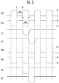
- FIG. 5 is a waveform view of the first to fourth clock signals and the first and second scan signals according to an embodiment of the present disclosure.
- first scan signals being supplied to the first first scan line S 11 and the second first scan line S 12
- second scan signals being supplied to the first second scan line S 21 and the second second scan line S 22 are illustrated for convenience of explanation.
- the timing controller 270 may supply clock signals CLK 1 , CLK 2 , CLK 3 , CLK 4 having the same signal characteristics.
- the clock signals CLK 1 , CLK 2 , CLK 3 and CLK 4 may be clock signals that swing between a first voltage V 1 that is a low voltage and a second voltage V 2 that is a high voltage.
- the first clock signal CLK 1 may be set to the same signal as the third clock signal CLK 3
- the second clock signal CLK 2 may be set to the same signal as the fourth clock signal CLK 4 .
- the timing controller 270 may further reduce the brightness difference by altering the clock signals CLK 1 , CLK 2 , CLK 3 , CLK 4 .
- the timing controller 270 may alter at least one of a pulse width, a length of a rising edge period, and a length of a falling edge period.
- FIG. 6 is a waveform view of the third and fourth clock signals and the second scan signal according to the embodiment of the present disclosure.
- FIG. 6 only the second scan signals being supplied to the first second scan line S 21 and the second second scan line S 22 are illustrated for convenience of explanation.
- a pulse width Pw 3 of the third clock signal CLK 3 may be set to be different from a pulse width Pw 1 of the first clock signal CLK 1 .
- the pulse width Pw 3 of the third clock signal CLK 3 may be set to be smaller than the pulse width Pw 1 of the first clock signal CLK 1 .
- a pulse width Pw 4 of the fourth clock signal CLK 4 may be set to be different from the pulse width Pw 2 of the second clock signal CLK 2 .
- the pulse width Pw 4 of the fourth clock signal CLK 4 may be set to be smaller than the pulse width Pw 2 of the second clock signal CLK 2 .
- the pulse width Pw 1 of the first clock signal CLK 1 and the pulse width Pw 2 of the second clock signal CLK 2 may be the same, and the pulse width Pw 3 of the third clock signal CLK 3 and the pulse width Pw 4 of the fourth clock signal CLK 4 may be the same.
- the supplying period (or pulse width) of the second scan signal may be reduced as illustrated in FIG. 6 .
- the data entry time of the second pixels PXL 2 may be adjusted to be similar to the data entry time of the first pixels PXL 1 , and accordingly, the difference of brightness between the first pixel area AA 1 and the second pixel area AA 2 may be reduced.
- FIG. 7 is a waveform view of the third and fourth clock signals and the second scan signal according to another embodiment of the present disclosure.
- FIG. 7 only the second scan signals being supplied to the first second scan line S 21 and the second second scan line S 22 are illustrated for convenience of explanation.
- a falling edge period F 3 of the third clock signal CLK 3 may be set to be different from a falling edge period F 1 of the first clock signal CLK 1 .
- the falling edge period F 3 of the third clock signal CLK 3 may be set to be longer than the falling edge period F 1 of the first clock signal CLK 1 .
- a rising edge period R 3 of the third clock signal CLK 3 may be set to be different from a rising edge period R 1 of the first clock signal CLK 1 .
- the rising edge period R 3 of the third clock signal CLK 3 may be set to be longer than the rising edge period R 1 of the first clock signal CLK 1 .
- the first clock signal CLK 1 illustrated in FIG. 5 is an ideal clock signal, and its falling edge period F 1 and the rising edge period R 1 may be set to “0”. However, an actual first clock signal CLK 1 may have a falling edge period F 1 and a rising edge period R 1 having a predetermined length due to an RC component of the actual first clock line 241 .
- a falling edge period F 4 of the fourth clock signal CLK 4 may be set to be different from a falling edge period F 2 of the second clock signal CLK 2 .
- the falling edge period F 4 of the fourth clock signal CLK 4 may be set to be longer than the falling edge period F 2 of the second clock signal CLK 2 .
- a rising edge period R 4 of the fourth clock signal CLK 4 may be set to be different from a rising edge period R 2 of the second clock signal CLK 2 .
- the rising edge period R 4 of the fourth clock signal CLK 4 may be set to be longer than the rising edge period R 2 of the second clock signal CLK 2 .
- the second clock signal CLK 2 illustrated in FIG. 5 is an ideal clock signal, and its falling edge period R 2 and the rising edge period R 2 may be set to “0”. However, the actual second clock signal CLK 2 may have a falling edge period F 2 and a rising edge period R 2 having a predetermined length by the RC component of the second clock line 242 .
- the falling edge period F 1 and the rising edge period R 1 of the first clock signal CLK 1 may have the same length as the falling edge period F 2 and the rising edge period R 2 of the second clock signal CLK 2 , respectively.
- the falling edge period F 3 and the rising edge period R 3 of the third clock signal CLK 3 may have the same length as the falling edge period F 4 and the rising edge period R 4 of the fourth clock signal CLK 4 , respectively.
- the third clock signal CLK 3 and the fourth clock signal CLK 4 may change from a second voltage V 2 (high voltage) to a first voltage V 1 (low voltage) via a third voltage V 3 (intermediate voltage) during the falling edge periods F 3 , F 4 , respectively.
- the third clock signal CLK 3 and the fourth clock signal CLK 4 may change from the first voltage V 1 (low voltage) to the second voltage V 2 (high voltage) via the third voltage V 3 (intermediate voltage) during the rising edge periods R 3 , R 4 , respectively.
- the third clock signal CLK 3 and the fourth clock signal CLK 4 may have a staircase wave form of swinging between the first voltage V 1 and the second voltage V 2 via the third voltage V 3 .
- the first voltage V 1 may be set to a negative voltage
- the second voltage V 2 may be set to a positive voltage
- the third voltage V 3 may be set to a ground voltage.
- FIG. 7 illustrates an embodiment where all the falling edge periods F 3 , F 4 and the rising edge periods R 3 , R 4 of the third and fourth clock signals CLK 3 , CLK 4 are adjusted, but only one of the falling edge periods F 3 , F 4 and the rising edge periods R 3 , R 4 may be adjusted instead.
- the supplying period (or pulse width) of the second scan signal may be reduced as illustrated in FIG. 7 , and the second scan signal may change in a similar form as the first scan signal as illustrated in FIG. 5 .
- the data entry time of the second pixels PXL 2 may be adjusted to be similar to the data entry time of the first pixels PXL 1 , and accordingly, the brightness difference between the first pixel area AA 1 and the second pixel area AA 2 may be reduced.
- FIG. 8 is a view illustrating an embodiment of the scan stage circuit illustrated in FIG. 4 .
- FIG. 8 illustrates the scan stage circuits SST 11 , SST 12 of the first scan driver 210 for convenience of explanation.
- the first scan stage circuit SST 11 may include a first driving circuit 1210 , a second driving circuit 1220 , and an output circuit 1230 .
- the output circuit 1230 may control a voltage being supplied to an output terminal 1006 in response to a voltage of a first node N 1 and a second node N 2 .
- the output circuit 1230 may include a fifth transistor M 5 and a sixth transistor M 6 .
- the fifth transistor M 5 may be connected between a fourth input terminal 1004 to which the first driving power source VDD 1 is input and an output terminal 1006 , and a gate electrode may be connected to the first node N 1 . Such a fifth transistor M 5 may control the connection of the fourth input terminal 1004 and the output terminal 1006 in response to the voltage being applied to the first node N 1 .
- the sixth transistor M 6 may be connected between the output terminal 1006 and a third input terminal 1003 , and a gate electrode may be connected to the second node N 2 . Such a sixth transistor M 6 may control the connection of the output terminal 1006 and the third input terminal 1003 in response to the voltage being applied to the second node N 2 .
- Such an output circuit 1230 may be driven by a buffer.
- the fifth transistor M 5 and/or the sixth transistor M 6 may include a plurality of transistors connected in parallel to one another.
- the first driving circuit 1210 may control a voltage of a third node N 3 in response to signals being supplied to the first input terminal 1001 to the third input terminal 1003 .
- the first driving circuit 1210 may include a second transistor M 2 to a fourth transistor M 4 .
- the second transistor M 2 may be connected between the first input terminal 1001 and the third node N 3 , and a gate electrode may be connected to the second input terminal 1002 . Such a second transistor M 2 may control the connection of the first input terminal 1001 and the third node N 3 in response to the signal being supplied to the second input terminal 1002 .
- the third transistor M 3 and the fourth transistor M 4 may be connected in series between the third node N 3 and the fourth input terminal 1004 .
- the third transistor M 3 may be connected between the fourth transistor M 4 and the third node N 3 , and a gate electrode may be connected to the third input terminal 1003 .
- Such a third transistor M 3 may control the connection of the fourth transistor M 4 and the third node N 3 in response to the signal being supplied to the third input terminal 1003 .
- the fourth transistor M 4 may be connected between the third transistor M 3 and the fourth input terminal 1004 , and a gate electrode may be connected to the first node N 1 . Such a fourth transistor M 4 may control the connection of the third transistor M 3 and the fourth input terminal 1004 in response to the voltage of the first node N 1 .
- the second driving circuit 1220 may control the voltage of the first node N 1 in response to the second input terminal 1002 and the voltage of the third node N 3 .
- the second driving circuit 1220 may include a first transistor M 1 , a seventh transistor M 7 , an eighth transistor M 8 , a first capacitor C 1 and a second capacitor C 2 .
- the first capacitor C 1 may be connected between the second node N 2 and the output terminal 1006 . Such a first capacitor C 1 charges a voltage corresponding to a turn-on and turn-off of the sixth transistor M 6 .
- the second capacitor C 2 may be connected between the first node N 1 and the fourth input terminal 1004 . Such a second capacitor C 2 may charge a voltage being applied to the first node N 1 .
- the seventh transistor M 7 may be connected between the first node N 1 and the second input terminal 1002 , and a gate electrode may be connected to the third node N 3 . Such a seventh transistor M 7 may control the connection of the first node N 1 and the second input terminal 1002 in response to the voltage of the third node N 3 .
- the eighth transistor M 8 may be disposed between the first node N 1 and the fifth input terminal 1005 to which the second driving power source VSS 1 is supplied, and a gate electrode may be connected to the second input terminal 1002 . Such an eighth transistor M 8 may control the connection of the first node N 1 and the fifth input terminal 1005 in response to the signal of the second input terminal 1002 .
- the first transistor M 1 may be connected between the third node N 3 and the second node N 2 , and a gate electrode may be connected to the fifth input terminal 1005 . Such a first transistor M 1 may maintain an electrical connection of the third node N 3 and the second node N 2 while maintaining a turn-on state. In addition, the first transistor M 1 may limit a voltage falling width of the third node N 3 in response to the voltage of the second node N 2 . In other words, Even if the voltage of the second node N 2 falls below the second driving power source VSS 1 , the voltage of the third node N 3 does not fall below a voltage value obtained by subtracting a threshold voltage of the first transistor M 1 from the second driving power source VSS 1 . This will be explained in further detail hereinafter.
- the second scan stage circuit SST 12 and the rest of the scan stage circuits SST 13 ⁇ SST 1 k may have the same configuration as the first scan stage circuit SST 11 .
- the second input terminal 1002 of a j th (j being an odd number or an even number) scan stage circuit SST 1 j may be supplied with the first clock signal CLK 1
- the third input terminal of the j th scan stage circuit SST 1 j may be supplied with the second clock signal CLK 2
- the second input terminal 1002 of a j+1 th scan stage circuit SST 1 j+ 1 may be supplied with the second clock signal CLK 2
- the third input terminal 1003 of the j+1 th scan stage circuit SST 1 j+ 1 may be supplied with the first clock signal CLK 1 .
- FIG. 8 illustrates the stage circuits included in the first scan driver 210 , but the stage circuits included in the second scan driver 220 may have the same configuration.
- the second scan driver 220 may use the third clock signal CLK 3 and the fourth clock signal CLK 4 instead of the first clock signal CLK 1 and the second clock signal CLK 2 .
- FIG. 9 is a view illustrating an embodiment of the first pixel illustrated in FIG. 2 .
- FIG. 9 illustrates the first pixel PXL 1 connected to an m th first data line D 1 m and an i th first scan line S 1 i for convenience of explanation.
- the first pixel PXL 1 may include an organic light emitting diode OLED, a first transistor T 1 to a seventh transistor T 7 and a storage capacitor Cst.
- An anode of the organic light emitting diode OLED may be connected to the first transistor T 1 via the sixth transistor T 6 , and a cathode of the organic light emitting diode OLED may be connected to the second pixel power source ELVSS.
- Such an organic light emitting diode OLED may generate light of a certain brightness in response to the amount of current being supplied from the first transistor T 1 .
- the first pixel power source ELVDD may be set to a higher voltage than the second pixel power source ELVSS so that a current may flow to the organic light emitting diode OLED.
- the first pixel power source ELVDD may be set to a positive voltage
- the second pixel power source ELVSS may be set to a negative voltage
- the seventh transistor T 7 may be connected between the initialization power source and the anode of the organic light emitting diode OLED. Further, the gate electrode of the seventh transistor T 7 may be connected to the i th first scan line S 1 i . Such a seventh transistor T 7 may be turned-on when a scan signal is supplied to the i th first scan line S 1 i , and supply the voltage of the initialization power source Vint to the anode of the organic light emitting diode OLED.
- the initialization power source Vint may be set to a lower voltage than the data signal.
- the sixth transistor T 6 may be connected between the first transistor T 1 and the anode of the organic light emitting diode OLED. Further, the gate electrode of the sixth transistor T 6 may be connected to the i th first emission control line E 1 i . Such a sixth transistor T 6 may be turned-off when the emission control signal is supplied to the i th first emission control line E 1 i , but turned-on in other cases.
- the fifth transistor T 5 may be connected between the first pixel power source ELVDD and the first transistor T 1 . Further, the gate electrode of the fifth transistor T 5 may be connected to the i th first emission control line E 1 i . Such a fifth transistor T 5 may be turned-off when a emission control signal is supplied to the i th first emission control line E 1 i , but turned-on in other cases.
- a first electrode of the first transistor T 1 may be connected to the first pixel power source ELVDD via the fifth transistor T 5 , and a second electrode of the first transistor T 1 may be connected to the anode of the organic light emitting diode OLED via the sixth transistor T 6 . Further, the gate electrode of the first transistor T 1 may be connected to a tenth node N 10 . Such a first transistor T 1 may control the amount of current flowing from the first pixel power source ELVDD to the second pixel power source ELVSS via the organic light emitting diode OLED in response to the voltage of the tenth node N 10 .
- the third transistor T 3 may be connected between the second electrode of the first transistor T 1 and the tenth node N 10 . Further, the gate electrode of the third transistor T 3 may be connected to the i th first scan line S 1 i . Such a third transistor T 3 may be turned-on when a scan signal is supplied to the i th first scan line S 1 i , and electrically connect the second electrode of the first transistor T 1 and the tenth node N 10 . Therefore, when the third transistor T 3 is turned-on, the first transistor T 1 may be connected in a diode form.
- the fourth transistor T 4 may be connected between the tenth node N 10 and the initialization power source Vint. Further, the gate electrode of the fourth transistor T 4 may be connected to the i ⁇ 1 th first scan line S 1 i ⁇ 1. Such a fourth transistor T 4 may be turned-on when a scan signal is supplied to the i ⁇ 1 th first scan line S 1 i ⁇ 1, and supply the voltage of the initialization power source Vint to the tenth node N 10 .
- the second transistor T 2 may be connected between the m th first data line D 1 m and the first electrode of the first transistor T 1 . Further, the gate electrode of the second transistor T 2 may be connected to the i th first scan line S 1 i . Such a second transistor T 2 may be turned-on when a scan signal is supplied to the i th first scan line S 1 i , and electrically connect the m th first data line D 1 m and the first electrode of the first transistor T 1 .
- the storage capacitor Cst may be connected between the first pixel power source ELVDD and the tenth node N 10 . Such a storage capacitor Cst may store a voltage corresponding to the data signal and the threshold voltage of the first transistor T 1 .
- the second pixel PXL 2 may have the same circuit as the first pixel PXL 1 . Therefore, detailed explanation on the second pixel PXL 2 will be omitted.
- the pixels PXL 1 , PXL 2 of the present disclosure are not limited to the aforementioned pixel structure.
- the pixel may have a circuit structure capable of supplying current to the organic light emitting diode OLED, and the structure may be selected from structures well known in the art.
- the organic light emitting diode OLED may generate lights of various colors such as red, green and blue light in response to the amount of current being supplied from the driving transistor, but there is no limitation thereto.
- the organic light emitting diode OLED may generate white light in response to the amount of current being supplied from the driving transistor.
- a color image may be realized using a separate color filter or the like.
- transistors in the present disclosure are P-type transistors for convenience of explanation, there is no limitation thereto. In other words, the transistors may be formed as N-type transistors.
- the gate off voltage and the gate on voltage of the transistors may be set to voltages of other levels depending on the type of the transistors.
- the gate off voltage and the gate on voltage may be set to a high level voltage and a low level voltage, respectively, and in the case of an N-type transistor, the gate off voltage and the gate on voltage may be set to a low level voltage and a high level voltage, respectively.
- FIG. 10 is a view illustrating a display device according to an embodiment of the present disclosure.
- the display device 10 may include pixel areas AA 1 , AA 2 , AA 3 , peripheral areas NA 1 , NA 2 , NA 3 , and pixels PXL 1 , PXL 2 , PXL 3 .
- the third pixel area AA 3 may be disposed at one side of the second pixel area AA 2 . Accordingly, the second pixel area AA 2 may be disposed between the first pixel area AA 1 and the third pixel area AA 3 , and the first pixel area AA 1 and the third pixel area AA 3 may be disposed such that they are spaced apart from each other.
- the third pixel area AA 3 may have a smaller surface area than the first pixel area AA 1 .
- a width W 3 of the third pixel area AA 3 may be set to be smaller than a width W 1 of the first pixel area AA 1
- a length L 3 of the third pixel area AA 3 may be set to be shorter than a length L 1 of the first pixel area AA 1 .
- the third pixel area AA 3 may have a smaller surface area than the second pixel area AA 2 .
- the width W 3 of the third pixel area AA 3 may be set to be smaller than the width W 2 of the second pixel area AA 2
- the length L 3 of the third pixel area AA 3 may be set to be shorter than the length L 2 of the second pixel area AA 2 .
- the surface area of the third pixel area AA 3 may be set to be greater than the second pixel area AA 2 .
- the third peripheral area NA 3 may exist on a periphery of the third pixel area AA 3 , and may surround at least a portion of the third pixel area AA 3 .
- the width of the third peripheral area NA 3 may be set to be same overall. However, there is no limitation thereto, and thus the width of the third peripheral area NA 3 may be set differently depending on its location.
- the third pixels PXL 3 may be disposed in the third pixel area AA 3 , and each of the third pixels PXL 3 may be connected to a third scan line S 3 , a third emission control line E 3 , and a third data line D 3 . When necessary, each of the third pixels PXL 3 may be connected to a plurality of scan lines.
- the third pixels PXL 3 may emit light of a certain brightness according to a control by the display driver 200 , and for this purpose, the third pixels PXL 3 may include a light emitting element, for example, organic light emitting diode.
- the display driver 200 may control the light emission of the pixels PXL 1 , PXL 2 , PXL 3 by supplying driving signals to the pixels PXL 1 , PXL 2 , PXL 3 .
- the display driver 200 may supply a scan signal to the pixels PXL 1 , PXL 2 , PXL 3 through the scan lines S 1 , S 2 , S 3 , supply a emission control signal to the pixels PXL 1 , PXL 2 , PXL 3 through the emission control lines E 1 , E 2 , E 3 , and supply a data signal to the pixels PXL 1 , PXL 2 , PXL 3 through the data lines D 1 , D 2 , D 3 .
- the substrate 100 may be formed in various shapes such that the pixel areas AA 1 , AA 2 , AA 3 and the peripheral areas NA 1 , NA 2 , NA 3 may be set thereon.
- the substrate 100 may include a plate shape base substrate 101 , a first subsidiary substrate 102 extending from one end of the base substrate to one side, and a second subsidiary substrate 103 extending from one end of the first subsidiary substrate 102 to one side.
- the second subsidiary substrate 103 may have a smaller surface area than the first subsidiary substrate 102 .
- the width of the second subsidiary substrate 103 may be set to be smaller than the width of the first subsidiary substrate 102
- the length of the second subsidiary substrate 103 may be set to be shorter than the length of the first subsidiary substrate 102 .
- the third pixel area AA 3 may have various shapes.
- the third pixel area AA 3 may have a polygonal shape, circular shape or the like. Further, at least a portion of the third pixel area AA 3 may have a curve shape.
- the number of the third pixels PXL 3 disposed in one row may differ depending on its location.
- the third pixels PXL 3 may have the pixel structure of FIG. 9 mentioned above, but there is no limitation thereto.
- FIG. 11 is a view illustrating in further detail the display driver illustrated in FIG. 10 .
- the display driver 200 may include a first scan driver 210 , a second scan driver 220 , a third scan driver 230 , a data driver 260 , a timing controller 270 , a first emission driver 310 , a second emission driver 320 , and a third emission driver 330 .
- the third scan driver 230 may supply a third scan signal to the third pixels PXL 3 through third scan lines S 31 ⁇ S 3 h.
- the third scan driver 230 may supply the third scan signal to the third scan lines S 31 ⁇ S 3 h sequentially.
- the third scan driver 230 may be disposed in the third peripheral area NA 3 .
- the third scan driver 230 may operate in response to a third scan control signal SCS 3 .
- the data driver 260 may supply a data signal to the third pixels PXL 3 through third data lines D 31 ⁇ D 3 q.
- the third pixels PXL 3 may be connected to the first pixel power source ELVDD and the second pixel power source ELVSS. When necessary, the third pixels PXL 3 may be additionally connected to the initialization power source Vint.
- Such third pixels PXL 3 may be supplied with the data signal from the third data lines D 31 ⁇ D 3 q when a third scan signal is supplied to the third scan lines S 31 ⁇ S 3 h , and the third pixels PXL 3 supplied with the data signal may control the amount of current flowing from the first pixel power source ELVDD to the second pixel power source ELVSS via the organic light emitting diode (not illustrated).
- the number of the third pixels PXL 3 disposed in one row may differ depending on its location.
- the third data lines D 31 ⁇ D 3 q may be connected to some of the second data lines D 21 ⁇ D 2 p ⁇ 1.
- the second data lines D 21 ⁇ D 2 p may be connected to some of the first data lines D 11 ⁇ D 1 m.
- the third emission driver 330 may supply a third emission control signal to the third pixels PXL 3 through third emission control lines E 31 ⁇ E 3 h.
- the third emission driver 330 may supply the third emission control signal to the third emission control lines E 31 ⁇ E 3 h sequentially.
- the third emission driver 330 may be disposed in the third peripheral area NA 3 .
- the third emission driver 330 may operate in response to the third emission control signal ECS 3 .
- the third emission driver 330 and the third emission control lines E 31 ⁇ E 3 h may be omitted.
- the number of the third pixels PXL 3 may be smaller than the number of the first pixels PXL 1 , and the lengths of the third scan lines S 31 ⁇ S 3 h and the third emission control lines E 31 ⁇ E 3 h may be shorter than the first scan lines S 11 ⁇ S 1 k and the first emission control lines E 11 ⁇ E 1 k.
- the number of the third pixels PXL 3 connected to any one of the third scan lines S 31 ⁇ S 3 h may be smaller than the number of the first pixels PXL 1 connected to any one of the first scan lines S 11 ⁇ S 1 k.
- the number of the third pixels PXL 3 connected to any one of the third emission control lines E 31 ⁇ E 3 h may be smaller than the number of the first pixels PXL 1 connected to any one of the first emission control lines E 11 ⁇ E 1 k.
- the number of the third pixels PXL 3 may be smaller than the number of the second pixels PXL 2
- the lengths of the third scan lines S 31 ⁇ S 3 h and the third emission control lines E 31 ⁇ E 3 h may be shorter than the second scan lines S 21 ⁇ S 2 j and the second emission control lines E 21 ⁇ E 2 j.
- the number of the third pixels PXL 3 connected to any one of the third scan lines S 31 ⁇ S 3 h may be smaller than the number of the second pixels PXL 2 connected to any one of the second scan lines S 21 ⁇ S 2 j.
- the number of the third pixels PXL 3 connected to any one of the third emission control lines E 31 ⁇ E 3 h may be smaller than the number of the second pixels PXL 2 connected to any one of the second emission control lines E 21 ⁇ E 2 j.
- the timing controller 270 may supply the third scan control signal SCS 3 and the third emission control signal ECS 3 to the third scan driver 230 and the third emission driver 330 , respectively, in order to control the third scan driver 230 and the third emission driver 330 .
- the third scan control signal SCS 3 and the third emission control signal ECS 3 may each include at least one clock signal and a start pulse.
- FIG. 12 is a view illustrating in further detail the first to third scan drivers illustrated in FIG. 11 .
- FIG. 12 explanation will be made with a main focus on components that are different from the aforementioned embodiment (for example, FIG. 4 ), and explanation on components overlapping the aforementioned embodiment will be omitted. Accordingly, hereinafter, explanation will be made based on the third scan driver 230 .
- a fifth clock line 245 and a sixth clock line 246 associated with the third scan driver 230 may be disposed such that they are electrically separated from other clock lines 241 , 242 , 243 , 244 .
- the fifth clock line 245 and the sixth clock line 246 may be connected between the timing controller 270 and the third scan driver 230 , and may respectively transmit a fifth clock signal CLK 5 and a sixth clock signal CLK 6 supplied from the timing controller 270 to the third scan driver 230 .
- the fifth clock signal CLK 5 and the sixth clock signal CLK 6 may have different phases.
- the sixth clock signal CLK 6 may have a phase difference of 180° compared to the fifth clock signal CLK 5 . That is, the sixth clock signal CLK 6 may be an inverted clock signal of the fifth clock signal CLK 5 .
- the third scan driver 230 may include a plurality of scan stage circuits SST 31 ⁇ SST 3 h.
- Each of the scan stage circuits SST 31 ⁇ SST 3 h of the third scan driver 230 may be connected to one end of the third scan lines S 31 ⁇ S 3 h , and may supply a third scan signal to the third scan lines S 31 ⁇ S 3 h.
- the scan stage circuits SST 31 ⁇ SST 3 h may operate in response to the clock signals CLK 5 , CLK 6 being supplied from the timing controller 270 . Further, the scan stage circuits SST 31 ⁇ SST 3 h may have the same configuration.
- the scan stage circuits SST 31 ⁇ SST 3 h may be supplied with an output signal (that is, scan signal) or a start pulse SSP 3 of a previous scan stage circuit.
- the first scan stage circuit SST 31 may be supplied with the start pulse SSP 3 , and the rest of the scan stage circuits SST 32 ⁇ SST 3 h may be supplied with an output signal of the previous stage circuit.
- the last scan stage circuit SST 3 h of the third scan driver 230 may supply an output signal to the first scan stage circuit SST 21 of the second scan driver 220 .
- Each of the scan stage circuits SST 31 ⁇ SST 3 h may be supplied with a first driving power source VDD 1 and a second driving power source VSS 1 .
- FIG. 12 illustrates that the scan drivers 210 , 220 , 230 each use two clock signals, but the number of clock signals that the scan drivers 210 , 220 , 230 use may differ depending on the structure of the scan stage circuit.
- FIG. 13 is a waveform view of the fifth and sixth clock signals and the third scan signal according to an embodiment of the present disclosure.
- FIG. 13 illustrates only the third scan signals that are supplied to the first third scan line S 31 and the second third scan line S 32 , for convenience of explanation.
- the characteristics of the fifth and sixth clock signals CLK 5 , CLK 6 may be set to be different from the first and second clock signals CLK 1 , CLK 2 .
- a pulse width Pw 5 of the fifth clock signal CLK 5 may be set to be smaller than the pulse width Pw 1 of the first clock signal CLK 1 .
- a pulse width Pw 6 of the sixth clock signal CLK 6 may be set to different from the pulse width Pw 2 of the second clock signal CLK 2 .
- the pulse width Pw 6 of the sixth clock signal CLK 6 may be set to be smaller than the pulse width Pw 2 of the second clock signal CLK 2 .
- the pulse width Pw 5 of the fifth clock signal CLK 5 and the pulse width Pw 6 of the sixth clock signal CLK 6 may be the same.
- the supplying period (or pulse width) of the third scan signal S 31 and S 32 may be reduced as illustrated in FIG. 13 .
- the data entry time of the third pixels PXL 3 may be adjusted to be similar to the data entry time of the first pixels PXL 1 , and accordingly, the difference of brightness between the first pixel area AA 1 and the third pixel area AA 3 may be reduced.
- loads of the third scan lines S 31 ⁇ S 3 h and loads of the second scan lines S 21 ⁇ S 2 j may be different from each other.
- the characteristics of the fifth and sixth clock signals CLK 5 , CLK 6 may be set to be different from the third and fourth clock signals CLK 3 , CLK 4 .
- the pulse width Pw 5 of the fifth clock signal CLK 5 may be set to be smaller than the pulse width Pw 3 of the third clock signal CLK 3
- the pulse width Pw 6 of the sixth clock signal CLK 6 may be set to be smaller than the pulse width Pw 4 of the fourth clock signal CLK 4 .
- FIG. 14 is a waveform view illustrating the fifth and sixth clock signals and the third scan signal according to another embodiment of the present disclosure.
- FIG. 14 illustrates only the third scan signals being supplied to the first third scan line S 31 and the second third scan line S 32 , for convenience of experience.
- a falling edge period F 5 of the fifth clock signal CLK 5 may be set to be different from the falling edge period F 1 of the first clock signal CLK 1 .
- the falling edge period F 5 of the fifth clock signal CLK 5 may be set to be longer than the falling edge period F 1 of the first clock signal CLK 1 .
- a rising edge period R 5 of the fifth clock signal CLK 5 may be set to be different from the rising edge period R 1 of the first clock signal CLK 1 .
- the rising edge period R 5 of the fifth clock signal CLK 5 may be set to be longer than the rising edge period R 1 of the first clock signal CLK 1 .
- a falling edge period F 6 of the sixth clock signal CLK 6 may be set to be different from the falling edge period F 2 of the second clock signal CLK 2 .
- the falling edge period F 6 of the sixth clock signal CLK 6 may be set to be longer than the falling edge period F 2 of the second clock signal CLK 2 .
- a rising edge period R 6 of the sixth clock signal CLK 6 may be set to be different from the rising edge period R 2 of the second clock signal CLK 2 .
- the rising edge period R 6 of the sixth clock signal CLK 6 may be set to be longer than the rising edge period R 2 of the second clock signal CLK 2 .
- the falling edge period R 5 and rising edge period R 5 of the of the fifth clock signal CLK 5 may have the same length as the falling edge period R 6 and the rising edge period R 6 of the sixth clock signal CLK 6 , respectively.
- the fifth clock signal CLK 5 and the sixth clock signal CLK 6 may change from the second voltage V 2 (high voltage) to the first voltage V 1 (low voltage) via the third voltage V 3 (intermediate voltage) during the falling edge periods F 5 , F 6 , respectively.
- the fifth clock signal CLK 5 and the sixth clock signal CLK 6 may change from the first voltage V 1 (low voltage) to the second voltage V 2 (high voltage) via the third voltage V 3 (intermediate voltage) during the rising edge periods R 5 , R 6 , respectively.
- the fifth clock signal CLK 5 and the sixth clock signal CLK 6 may have the staircase wave form which swings between the first voltage V 1 and the second voltage V 2 via the third voltage V 3 .
- the supplying period (or pulse width) of the third scan signal may also be reduced as illustrated in FIG. 14 , and the third scan signal may change in a similar form as the first scan signal illustrated in FIG. 5 .
- the data entry time of the third pixels PXL 3 may be adjusted to be similar to the data entry time of the first pixels PXL 1 , and accordingly, the difference of brightness between the first pixel area AA 1 and the third pixel area AA 3 may be reduced.
- the loads of the third scan lines S 31 ⁇ S 3 h and the loads of the second scan lines S 21 ⁇ S 2 j may be different from each other.
- the falling edge period F 5 and the rising edge period R 5 of the fifth clock signal CLK 5 may be formed to be longer than the falling edge period F 3 and the rising edge period R 3 of the third clock signal CLK 3 , respectively.
- the duration time of the third voltage V 3 may be extended during the falling edge period F 5 and the rising edge period R 5 of the fifth clock signal CLK 5 .
- the falling edge period F 6 and the rising edge period R 6 of the sixth clock signal CLK 6 may be formed to be longer than the falling edge period F 4 and the rising edge period R 4 of the fourth clock signal CLK 4 , respectively.
- the duration time of the third voltage V 3 may be extended during the falling edge period F 6 and the rising edge period R 6 of the sixth clock signal CLK 6 .
- FIG. 15 is a view illustrating a display device according to an embodiment of the present disclosure.
- FIG. 15 explanation will be made with a main focus on components that are different from the aforementioned embodiment (for example, FIG. 2 and FIG. 10 ), and explanation on components overlapping the aforementioned embodiment will be omitted. Accordingly, hereinafter, explanation will be made based on the third pixel area AA 3 and the third pixels PXL 3 .
- the display device 10 may include the pixel areas AA 1 , AA 2 , AA 3 , the peripheral areas NA 1 , NA 2 , NA 3 , and the pixels PXL 1 , PXL 2 , PXL 3 .
- the second pixel area AA 2 and the third pixel area AA 3 may be disposed at one side of the first pixel area AA 1 .
- the second pixel area AA 2 and the third pixel area AA 3 may be disposed such that they are spaced apart from each other.
- the first pixel area AA 1 may have a greater surface area than the second pixel area AA 2 and the third pixel area AA 3 .
- the width W 1 of the first pixel area AA 1 may be set to be greater than the widths W 2 , W 3 of the other pixel areas AA 2 , AA 3
- the length L 1 of the first pixel area AA 1 may be set to be greater than the lengths L 2 , L 3 of the other pixel areas AA 2 , AA 3 .
- the second pixel area AA 2 and the third pixel area AA 3 may each have a smaller surface area than, the same surface area as, or a different surface area from the first pixel area AA 1 .
- the width W 2 of the second pixel area AA 2 may be set to be the same as or different from the width W 3 of the third pixel area AA 3
- the length L 2 of the second pixel area AA 2 may be set to be the same as or different from the length L 3 of the third pixel area AA 3 .
- the substrate 100 may be formed in various shapes such that the aforementioned pixel areas AA 1 , AA 2 , AA 3 and the peripheral areas NA 1 , NA 2 , NA 3 may be set thereon.
- the substrate 100 may include the plate shape base substrate 101 , the first subsidiary substrate 102 and the second subsidiary substrate 103 extending from one end of the base substrate 101 to one side.
- the first subsidiary substrate 102 and the second subsidiary substrate 103 may be formed integrally with the base substrate 101 , and a concave part 104 may exist between the first subsidiary substrate 102 and the second subsidiary substrate 103 .
- the concave part 104 may be an area of the substrate 100 of which a portion has been removed, whereby the first subsidiary substrate 102 and the second subsidiary substrate 103 may be spaced apart from each other.
- the first subsidiary substrate 102 and the second subsidiary substrate 103 may each have a smaller surface area than, the same surface area as, or a different surface area from the base substrate 101 .
- the first subsidiary substrate 102 and the second subsidiary substrate 103 may be formed in various shapes such that the pixel areas AA 2 , AA 3 and the peripheral areas NA 2 , NA 3 may be set thereon.
- the aforementioned first pixel area AA 1 and the first peripheral area NA 1 may be defined on the base substrate 101
- the second pixel area AA 2 and the second peripheral area NA 2 may be defined on the first subsidiary substrate 102
- the third pixel area AA 3 and the third peripheral area NA 3 may be defined on the second subsidiary substrate 103 .
- the first pixel area AA 1 may have various shapes.
- the first pixel area AA 1 may have a polygonal shape, circular shape or the like. Further, at least a portion of the first pixel area AA 1 may have a curve shape.
- the second pixel area AA 2 and the third pixel area AA 3 may each have various shapes.
- the second pixel area AA 2 and the third pixel area AA 3 may have a polygonal shape, circular shape or the like. Further, at least a portion of the second pixel area and the third pixel area AA 3 may have a curve shape.
- corner parts of each of the second pixel area AA 2 and the third pixel area AA 3 may have an angular shape, an inclined shape and a curve shape and the like.
- FIG. 16 is a detailed view of the display driver illustrated in FIG. 15 .
- the display driver 200 may include the first scan driver 210 , the second scan driver 220 , the third scan driver 230 , the data driver 260 , the timing controller 270 , the first emission driver 310 , the second emission driver 320 , and the third emission driver 330 .
- the third scan driver 230 may supply the third scan signal to the third pixels PXL 3 through the third scan lines S 31 ⁇ S 3 h.
- the third scan driver 230 may supply the third scan signal to the third scan lines S 31 ⁇ S 3 h , sequentially.
- the third scan driver 230 may be disposed in the third peripheral area NA 3 .
- the third scan driver 230 may operate in response to the third scan control signal SCS 3 .
- the data driver 260 may supply the data signal to the third pixels PXL 3 through the third data lines D 31 ⁇ D 3 q.
- the third pixels PXL 3 may be connected to the first pixel power source ELVDD and the second pixel power source ELVSS. When necessary, the third pixels PXL 3 may be additionally connected to the initialization power source Vint.
- Such third pixels PXL 3 may be supplied with the data signal from the third data lines D 31 ⁇ D 3 q when the third scan signal is being supplied to the third scan lines S 31 ⁇ S 3 h , and the third pixels PXL 3 supplied with the data signal may control the amount of current flowing from the first pixel power source ELVDD to the second pixel power source ELVSS via the organic light emitting diode (not illustrated).
- the number of the third pixels PXL 3 disposed in one row may differ depending on their location.
- the third data lines D 31 ⁇ D 3 q may be connected to some of the first data lines D 1 n+ 1 ⁇ D 1 o.
- the second data lines D 21 ⁇ D 2 p may be connected to some of the other first data lines D 11 ⁇ D 1 m ⁇ 1.
- the third emission driver 330 may supply the third emission control signal to the third pixels PXL 3 through the third emission control lines E 31 ⁇ E 3 h.
- the third emission driver 330 may supply the third emission control signal to the third emission control lines E 31 ⁇ E 3 h sequentially.
- the third emission driver 330 may be disposed in the third peripheral area NA 3 .
- the third emission driver 330 and the third emission control lines E 31 ⁇ E 3 h may be omitted.
- the third emission driver 330 may operate in response to the third emission control signal ECS 3 .
- the number of the third pixels PXL 3 may be smaller than the number of the first pixels PXL 1 , and the lengths of the third scan lines S 31 ⁇ S 3 h and the third emission control lines E 31 ⁇ E 3 h may be shorter than the first scan lines S 11 ⁇ S 1 k and the first emission control lines E 11 ⁇ E 1 k.
- the number of the third pixels PXL 3 connected to any one of the third scan lines S 31 ⁇ S 3 h may be smaller than the number of the first pixels PXL 1 connected to any one of the first scan line S 11 ⁇ S 1 k.
- the number of the third pixels PXL 3 connected to any one of the third emission control lines E 31 ⁇ E 3 h may be smaller than the number of the first pixels PXL 1 connected to any one of the first emission control lines E 11 ⁇ E 1 k.
- the timing controller 270 may supply the third scan control signal SCS 3 and the third emission control signal ECS 3 to the third scan driver 230 and the third emission driver 330 , respectively, in order to control the third scan driver 230 and the third emission driver 330 .
- the third scan control signal SCS 3 and the third emission control signal ECS 3 may each include at least one clock signal and a start pulse.
- FIG. 17 is a view illustrating in further detail the first to third scan drivers illustrated in FIG. 16 .
- explanation will be made with a main focus on components that are different from the aforementioned embodiment (for example, FIG. 4 and FIG. 12 ), and explanation on components overlapping the aforementioned embodiment will be omitted. Accordingly, hereinafter, explanation will be made based on the third scan driver 230 .
- the fifth clock line 245 and the sixth clock line 246 may be electrically separated from other clock lines 241 , 242 , 243 , 244 .
- the fifth clock line 245 and the sixth clock line 246 may be connected between the timing controller 270 and the third scan driver 230 to respectively transmit the fifth clock signal CLK 5 and the sixth clock signal CLK 6 being supplied from the timing controller 270 to the third scan driver 230 .
- the fifth clock signal CLK 5 and the sixth clock signal CLK 6 may have different phases.
- the sixth clock signal may have a phase difference of 180° compared to the fifth clock signal CLK 5 . That is, the sixth clock signal CLK 6 may be an inverted clock signal of the fifth clock signal CLK 5 .
- the third scan driver 230 may include a plurality of scan stage circuits SST 31 ⁇ SST 3 h.
- Each of the scan stage circuits SST 31 ⁇ SST 3 h of the third scan driver 230 may be connected to one end of the third scan lines S 31 ⁇ S 3 h , and may supply the third scan signal to the third scan lines S 31 ⁇ S 3 h.
- the scan stage circuits SST 31 ⁇ SST 3 h may operate in response to the clock signals CLK 5 , CLK 6 being supplied from the timing controller 270 . Further, the scan stage circuits SST 31 ⁇ SST 3 h may have the same configuration.
- the scan stage circuits SST 31 ⁇ SST 3 h may be supplied with an output signal (that is, scan signal) or a start pulse SSP 3 of a previous scan stage circuit.
- the first scan stage circuit SST 31 may be supplied with the start pulse SSP 3 , and the rest of the scan stage circuits SST 32 ⁇ SST 3 h may be supplied with the output signal of the previous stage circuit.
- the last scan stage circuit SST 3 h of the third scan driver 230 may supply the output signal to the first scan stage circuit SST 21 of the second scan driver 220 .
- Each of the scan stage circuits SST 31 ⁇ SST 3 h may be supplied with the first driving power source VDD 1 and the second driving power source VSS 1 .
- the scan drivers 210 , 220 , 230 each use two clock signals, but the number of the clock signals that the scan drivers 210 , 220 , 230 use may differ depending on the structure of the scan stage circuit.
- the characteristics of the fifth and sixth clock signals CLK 5 , CLK 6 may be set to be different from the first and second clock signals CLK 1 , CLK 2 .
- At least one of the pulse width of the fifth and sixth clock signals CLK 5 , CLK 6 , the length of the rising edge period and the length of the falling edge period may be set to be different from the first and second clock signals CLK 1 , CLK 2 .
- the characteristics of the fifth and sixth clock signals CLK 5 , CLK 6 may be set to be different from the third and fourth clock signals CLK 3 , CLK 4 .
- clock signals provide to different scan lines have a different signal characteristic, for example, different pulse widths, different lengths of a rising edge period or different length of a falling edge period.
- the pulse widths of the clock signals may be inversely proportional to the number of pixels connected to one signal line.
- the lengths of rising edge periods and falling edge periods may be inversely proportional to the number of pixels connected to one signal line.
- the display device may have an image of uniform brightness regardless the number of pixels connected to one signal line.
Abstract
Description
Claims (9)
Priority Applications (2)
| Application Number | Priority Date | Filing Date | Title |
|---|---|---|---|
| US17/335,032 US20210287628A1 (en) | 2016-06-01 | 2021-05-31 | Display device |
| US17/871,468 US11847973B2 (en) | 2016-06-01 | 2022-07-22 | Display device capable of displaying an image of uniform brightness |
Applications Claiming Priority (2)
| Application Number | Priority Date | Filing Date | Title |
|---|---|---|---|
| KR1020160068361A KR102513988B1 (en) | 2016-06-01 | 2016-06-01 | Display device |
| KR10-2016-0068361 | 2016-06-01 |
Related Child Applications (1)
| Application Number | Title | Priority Date | Filing Date |
|---|---|---|---|
| US17/335,032 Continuation US20210287628A1 (en) | 2016-06-01 | 2021-05-31 | Display device |
Publications (2)
| Publication Number | Publication Date |
|---|---|
| US20170352328A1 US20170352328A1 (en) | 2017-12-07 |
| US11024258B2 true US11024258B2 (en) | 2021-06-01 |
Family
ID=58992714
Family Applications (2)
| Application Number | Title | Priority Date | Filing Date |
|---|---|---|---|
| US15/587,192 Active 2037-06-25 US11024258B2 (en) | 2016-06-01 | 2017-05-04 | Display device capable of displaying an image of uniform brightness |
| US17/335,032 Abandoned US20210287628A1 (en) | 2016-06-01 | 2021-05-31 | Display device |
Family Applications After (1)
| Application Number | Title | Priority Date | Filing Date |
|---|---|---|---|
| US17/335,032 Abandoned US20210287628A1 (en) | 2016-06-01 | 2021-05-31 | Display device |
Country Status (6)
| Country | Link |
|---|---|
| US (2) | US11024258B2 (en) |
| EP (1) | EP3255629B1 (en) |
| JP (1) | JP6914736B2 (en) |
| KR (1) | KR102513988B1 (en) |
| CN (1) | CN107452313B (en) |
| TW (1) | TWI752960B (en) |
Cited By (3)
| Publication number | Priority date | Publication date | Assignee | Title |
|---|---|---|---|---|
| US11127364B2 (en) | 2018-12-28 | 2021-09-21 | Lg Display Co., Ltd. | Display apparatus |
| US20220335878A1 (en) * | 2021-04-14 | 2022-10-20 | Samsung Display Co., Ltd. | Gate driver and display device including the same |
| US11756486B2 (en) | 2019-07-01 | 2023-09-12 | Chengdu Boe Opteoelectronics Technology Co., Ltd. | Display panel, display device and driving method |
Families Citing this family (35)
| Publication number | Priority date | Publication date | Assignee | Title |
|---|---|---|---|---|
| KR102525548B1 (en) * | 2015-12-29 | 2023-04-26 | 삼성디스플레이 주식회사 | Display device and electronic device having the same |
| KR102511947B1 (en) | 2016-06-17 | 2023-03-21 | 삼성디스플레이 주식회사 | Stage and Organic Light Emitting Display Device Using the same |
| JP7110116B2 (en) * | 2017-01-16 | 2022-08-01 | 株式会社半導体エネルギー研究所 | semiconductor equipment |
| KR102397411B1 (en) * | 2017-09-28 | 2022-05-16 | 삼성디스플레이 주식회사 | Display device |
| CN107610645B (en) * | 2017-10-26 | 2020-04-28 | 上海天马有机发光显示技术有限公司 | OLED display panel, driving method thereof and display device |
| EP3477705B1 (en) * | 2017-10-30 | 2021-04-07 | LG Display Co., Ltd. | Display device |
| TWI636446B (en) | 2017-11-08 | 2018-09-21 | 友達光電股份有限公司 | Display panel |
| KR102460550B1 (en) * | 2017-12-04 | 2022-10-31 | 삼성디스플레이 주식회사 | Display panel |
| JP2019109371A (en) * | 2017-12-19 | 2019-07-04 | シャープ株式会社 | Active matrix type display device and its driving method |
| US11132953B2 (en) * | 2018-03-19 | 2021-09-28 | Sharp Kabushiki Kaisha | Display device |
| CN108682372A (en) * | 2018-04-03 | 2018-10-19 | 京东方科技集团股份有限公司 | Array substrate and its driving method, display device |
| CN110767134B (en) * | 2018-07-26 | 2023-05-16 | 瀚宇彩晶股份有限公司 | Slope regulating and controlling method suitable for waveform of grid driving circuit |
| CN110085645B (en) * | 2018-08-10 | 2021-05-25 | 友达光电股份有限公司 | Display device |
| TWI692665B (en) * | 2018-08-10 | 2020-05-01 | 友達光電股份有限公司 | Diplay device |
| WO2020049707A1 (en) * | 2018-09-07 | 2020-03-12 | シャープ株式会社 | Display device and method for driving same |
| WO2020065858A1 (en) * | 2018-09-27 | 2020-04-02 | シャープ株式会社 | Display device |
| CN109192125B (en) * | 2018-10-10 | 2022-02-08 | 友达光电(昆山)有限公司 | Array substrate |
| CN110767166B (en) * | 2018-10-31 | 2021-03-30 | 昆山国显光电有限公司 | Display screen and display terminal |
| KR102633064B1 (en) | 2018-11-12 | 2024-02-06 | 삼성디스플레이 주식회사 | Stage and emission control driver having the same |
| KR102640827B1 (en) * | 2018-12-03 | 2024-02-28 | 삼성디스플레이 주식회사 | Display device and driving method thereof |
| TWI688804B (en) * | 2018-12-13 | 2020-03-21 | 友達光電股份有限公司 | Display panel |
| CN109584770B (en) * | 2018-12-17 | 2022-02-08 | 武汉天马微电子有限公司 | Display panel and display device |
| TWI690912B (en) * | 2019-02-13 | 2020-04-11 | 友達光電股份有限公司 | Display panel and driving method |
| KR102651045B1 (en) * | 2019-03-19 | 2024-03-27 | 삼성디스플레이 주식회사 | Display device |
| CN112449712B (en) | 2019-07-01 | 2024-01-09 | 京东方科技集团股份有限公司 | Display panel, display driving method thereof and display device |
| WO2021000235A1 (en) | 2019-07-01 | 2021-01-07 | 京东方科技集团股份有限公司 | Display panel, display device and driving method |
| KR102570275B1 (en) * | 2019-07-01 | 2023-08-24 | 보에 테크놀로지 그룹 컴퍼니 리미티드 | Display panels and display devices |
| WO2021053707A1 (en) | 2019-09-17 | 2021-03-25 | シャープ株式会社 | Display device and method for driving same |
| WO2021117228A1 (en) | 2019-12-13 | 2021-06-17 | シャープ株式会社 | Display device and method for driving same |
| US11087663B1 (en) * | 2020-05-15 | 2021-08-10 | Novatek Microelectronics Corp. | Display device and driving method thereof for reducing difference in brightness between areas with different widths |
| CN111768713B (en) * | 2020-07-31 | 2022-01-14 | 武汉天马微电子有限公司 | Display panel and display device |
| KR20220037043A (en) * | 2020-09-16 | 2022-03-24 | 삼성디스플레이 주식회사 | Display device |
| WO2023060567A1 (en) | 2021-10-15 | 2023-04-20 | 京东方科技集团股份有限公司 | Display substrate and display apparatus |
| CN114639362B (en) * | 2022-04-27 | 2023-03-24 | 长沙惠科光电有限公司 | Scanning drive circuit, display module and display device |
| CN115311982A (en) * | 2022-08-30 | 2022-11-08 | 武汉天马微电子有限公司 | Display panel, driving method thereof and display device |
Citations (44)
| Publication number | Priority date | Publication date | Assignee | Title |
|---|---|---|---|---|
| US20030210215A1 (en) | 2002-05-08 | 2003-11-13 | Hiroyuki Takahashi | Liquid crystal display device and driving method therefor |
| US20050057477A1 (en) * | 2003-09-17 | 2005-03-17 | Young-Nam Yun | Display device having multiple image display units |
| US20060077191A1 (en) * | 2004-10-08 | 2006-04-13 | Industrial Technology Research Institute | Non-rectangle display |
| US20060119560A1 (en) | 2004-12-02 | 2006-06-08 | Samsung Electronics Co., Ltd. | Clock generating circuit and a display device having the same |
| US20060244387A1 (en) * | 2005-04-28 | 2006-11-02 | Park Young J | Organic light emitting display and method of driving the same |
| JP2007251504A (en) | 2006-03-15 | 2007-09-27 | Renesas Technology Corp | Complementary mos ic |
| US20070229433A1 (en) | 2006-03-30 | 2007-10-04 | Lg. Philips Lcd Co. Ltd. | Display device and driving method thereof |
| US20080088568A1 (en) * | 2006-10-13 | 2008-04-17 | Nec Lcd Technologies, Ltd | Display device |
| US7385598B2 (en) | 2003-06-27 | 2008-06-10 | Samsung Electronics, Co., Ltd. | Driver for operating multiple display devices |
| US20080278467A1 (en) * | 2007-05-09 | 2008-11-13 | In-Jae Hwang | Liquid crystal display having progressive and interlaced modes, and driving method of the liquid crystal display |
| JP2008292995A (en) | 2007-04-27 | 2008-12-04 | Nec Lcd Technologies Ltd | Non-rectangular display apparatus |
| US20090115795A1 (en) | 2007-11-06 | 2009-05-07 | Samsung Electronics Co., Ltd. | Incremental brightness compensation systems, devices and methods for organic light emitting display (oled) |
| US20090262051A1 (en) * | 2008-04-18 | 2009-10-22 | Se-Ho Kim | Organic light emitting display device |
| US20100085348A1 (en) * | 2008-10-08 | 2010-04-08 | Samsung Electronics Co., Ltd. | Display device and method of driving the same |
| US20100123708A1 (en) | 2008-11-19 | 2010-05-20 | Seungho Jang | Liquid crystal display |
| US20100321372A1 (en) * | 2008-02-19 | 2010-12-23 | Akihisa Iwamoto | Display device and method for driving display |
| JP2011039559A (en) | 2010-11-08 | 2011-02-24 | Hitachi Displays Ltd | Display apparatus |
| US20120113070A1 (en) * | 2010-11-08 | 2012-05-10 | Au Optronics Corp. | Gate driver circuit and arrangement method of the same |
| US20120112988A1 (en) * | 2010-11-08 | 2012-05-10 | Norio Nakanishi | Display device |
| US20120212517A1 (en) * | 2011-02-17 | 2012-08-23 | Jeong-Keun Ahn | Organic light-emitting display and method of driving the same |
| US8638280B2 (en) | 2007-04-27 | 2014-01-28 | Nlt Technologies, Ltd. | Non-rectangular display apparatus |
| US20140176407A1 (en) | 2012-12-24 | 2014-06-26 | Samsung Display Co., Ltd. | Display device |
| US20140253419A1 (en) | 2013-03-05 | 2014-09-11 | Semiconductor Energy Laboratory Co., Ltd. | Display device and electronic device |
| US20140347405A1 (en) * | 2013-05-22 | 2014-11-27 | Samsung Display Co., Ltd. | Pixel circuit and method for driving the same |
| JP2015014793A (en) | 2014-07-14 | 2015-01-22 | Nltテクノロジー株式会社 | Display device |
| US20160005346A1 (en) | 2014-07-07 | 2016-01-07 | Samsung Display Co., Ltd. | Display device |
| US20160111040A1 (en) * | 2014-10-16 | 2016-04-21 | Lg Display Co., Ltd. | Panel array for display device with narrow bezel |
| US20170061922A1 (en) * | 2015-08-26 | 2017-03-02 | Boe Technology Group Co., Ltd. | Shift register and driving method thereof, gate driving circuit and display apparatus |
| US20170116923A1 (en) * | 2015-10-22 | 2017-04-27 | Samsung Display Co., Ltd. | Gate driver and display device having the same |
| US20170154572A1 (en) * | 2015-12-01 | 2017-06-01 | Lg Display Co., Ltd. | Organic light emitting diode display |
| US20170195658A1 (en) * | 2015-12-31 | 2017-07-06 | Lg Display Co., Ltd. | Display Device for Personal Immersive Device |
| WO2017172375A1 (en) | 2016-03-28 | 2017-10-05 | Groturbel Research Llc | Light-emitting diode displays |
| EP3246911A1 (en) | 2016-05-19 | 2017-11-22 | Samsung Display Co., Ltd. | Display device |
| US20180174531A1 (en) * | 2016-04-08 | 2018-06-21 | Shenzhen China Star Optoelectronics Technology Co., Ltd. | Liquid Crystal Panel Driver and Method for Driving the Same |
| US10019949B2 (en) * | 2016-01-15 | 2018-07-10 | Boe Technology Group Co., Ltd. | Shift register unit, gate driving circuit, display panel and display device |
| US10115366B2 (en) * | 2012-09-28 | 2018-10-30 | Lg Display Co., Ltd. | Liquid crystal display device for improving the characteristics of gate drive voltage |
| US10157683B2 (en) * | 2015-04-29 | 2018-12-18 | Lg Display Co., Ltd. | Shift register using oxide transistor and display device using the same |
| US10181279B2 (en) * | 2015-10-27 | 2019-01-15 | Lg Display Co., Ltd. | Shift register and display device including the same |
| US10229646B2 (en) * | 2015-08-12 | 2019-03-12 | Shenzhen China Star Optoelectronics Technology Co., Ltd | Liquid crystal display driving system and method |
| US10242638B2 (en) * | 2015-11-05 | 2019-03-26 | Boe Technology Group Co., Ltd. | Display adjusting device, power source circuit, display device and display adjusting method |
| US10255861B2 (en) * | 2016-05-04 | 2019-04-09 | Boe Technology Group Co., Ltd. | Gate driving circuit, array substrate, display panel and driving method thereof |
| US10268293B2 (en) * | 2015-06-25 | 2019-04-23 | Innolux Corporation | Image display systems and gate driving circuits that include a compensation circuit and shift registers |
| US10338727B2 (en) * | 2014-03-10 | 2019-07-02 | Lg Display Co., Ltd. | Display device and method for driving same |
| US10490128B1 (en) * | 2018-06-05 | 2019-11-26 | Apple Inc. | Electronic devices having low refresh rate display pixels with reduced sensitivity to oxide transistor threshold voltage |
Family Cites Families (8)
| Publication number | Priority date | Publication date | Assignee | Title |
|---|---|---|---|---|
| US7117775B2 (en) * | 2002-12-12 | 2006-10-10 | Voith Paper Patent Gmbh | Method and apparatus for transferring a paper web |
| KR100976986B1 (en) * | 2003-11-18 | 2010-08-19 | 삼성전자주식회사 | Gate driver circuit and display device having the same |
| KR20060124160A (en) * | 2005-05-31 | 2006-12-05 | 삼성전자주식회사 | Liquid crystal display and its driving method |
| US20080008856A1 (en) * | 2005-12-05 | 2008-01-10 | Daily Way Enterprises Ltd. | Article stabilizing system and uses thereof |
| CN101802903A (en) * | 2007-10-04 | 2010-08-11 | 夏普株式会社 | Display device and display device drive method |
| CN101911560B (en) * | 2007-12-28 | 2015-04-15 | 日本电气株式会社 | Communication system, response notifying method and apparatus |
| KR102212423B1 (en) * | 2014-02-14 | 2021-02-04 | 삼성디스플레이 주식회사 | Driver circuit and display comprising the same |
| TWI604982B (en) * | 2016-07-18 | 2017-11-11 | 行安機電股份有限公司 | Torque detector |
-
2016
- 2016-06-01 KR KR1020160068361A patent/KR102513988B1/en active IP Right Grant
-
2017
- 2017-05-04 US US15/587,192 patent/US11024258B2/en active Active
- 2017-06-01 TW TW106118160A patent/TWI752960B/en active
- 2017-06-01 JP JP2017109326A patent/JP6914736B2/en active Active
- 2017-06-01 CN CN201710403410.4A patent/CN107452313B/en active Active
- 2017-06-01 EP EP17174077.2A patent/EP3255629B1/en active Active
-
2021
- 2021-05-31 US US17/335,032 patent/US20210287628A1/en not_active Abandoned
Patent Citations (50)
| Publication number | Priority date | Publication date | Assignee | Title |
|---|---|---|---|---|
| US20030210215A1 (en) | 2002-05-08 | 2003-11-13 | Hiroyuki Takahashi | Liquid crystal display device and driving method therefor |
| JP2003323164A (en) | 2002-05-08 | 2003-11-14 | Hitachi Displays Ltd | Liquid crystal display device and its driving method |
| US7385598B2 (en) | 2003-06-27 | 2008-06-10 | Samsung Electronics, Co., Ltd. | Driver for operating multiple display devices |
| US20050057477A1 (en) * | 2003-09-17 | 2005-03-17 | Young-Nam Yun | Display device having multiple image display units |
| US20060077191A1 (en) * | 2004-10-08 | 2006-04-13 | Industrial Technology Research Institute | Non-rectangle display |
| US20060119560A1 (en) | 2004-12-02 | 2006-06-08 | Samsung Electronics Co., Ltd. | Clock generating circuit and a display device having the same |
| JP2006166395A (en) | 2004-12-02 | 2006-06-22 | Samsung Electronics Co Ltd | Clock generation circuit and display device having the same |
| US20060244387A1 (en) * | 2005-04-28 | 2006-11-02 | Park Young J | Organic light emitting display and method of driving the same |
| JP2007251504A (en) | 2006-03-15 | 2007-09-27 | Renesas Technology Corp | Complementary mos ic |
| US20070229433A1 (en) | 2006-03-30 | 2007-10-04 | Lg. Philips Lcd Co. Ltd. | Display device and driving method thereof |
| US20080088568A1 (en) * | 2006-10-13 | 2008-04-17 | Nec Lcd Technologies, Ltd | Display device |
| JP2008292995A (en) | 2007-04-27 | 2008-12-04 | Nec Lcd Technologies Ltd | Non-rectangular display apparatus |
| US8638280B2 (en) | 2007-04-27 | 2014-01-28 | Nlt Technologies, Ltd. | Non-rectangular display apparatus |
| US20080278467A1 (en) * | 2007-05-09 | 2008-11-13 | In-Jae Hwang | Liquid crystal display having progressive and interlaced modes, and driving method of the liquid crystal display |
| KR101281681B1 (en) | 2007-11-06 | 2013-07-03 | 삼성디스플레이 주식회사 | apparatus and method of adjusting driving voltage for compensating luminance variation |
| US20090115795A1 (en) | 2007-11-06 | 2009-05-07 | Samsung Electronics Co., Ltd. | Incremental brightness compensation systems, devices and methods for organic light emitting display (oled) |
| US20100321372A1 (en) * | 2008-02-19 | 2010-12-23 | Akihisa Iwamoto | Display device and method for driving display |
| US20090262051A1 (en) * | 2008-04-18 | 2009-10-22 | Se-Ho Kim | Organic light emitting display device |
| US20100085348A1 (en) * | 2008-10-08 | 2010-04-08 | Samsung Electronics Co., Ltd. | Display device and method of driving the same |
| US20100123708A1 (en) | 2008-11-19 | 2010-05-20 | Seungho Jang | Liquid crystal display |
| JP2011039559A (en) | 2010-11-08 | 2011-02-24 | Hitachi Displays Ltd | Display apparatus |
| US20120112988A1 (en) * | 2010-11-08 | 2012-05-10 | Norio Nakanishi | Display device |
| US20120113070A1 (en) * | 2010-11-08 | 2012-05-10 | Au Optronics Corp. | Gate driver circuit and arrangement method of the same |
| US20120212517A1 (en) * | 2011-02-17 | 2012-08-23 | Jeong-Keun Ahn | Organic light-emitting display and method of driving the same |
| US10115366B2 (en) * | 2012-09-28 | 2018-10-30 | Lg Display Co., Ltd. | Liquid crystal display device for improving the characteristics of gate drive voltage |
| US20140176407A1 (en) | 2012-12-24 | 2014-06-26 | Samsung Display Co., Ltd. | Display device |
| JP2014197179A (en) | 2013-03-05 | 2014-10-16 | 株式会社半導体エネルギー研究所 | Display unit and electronic apparatus |
| US20140253419A1 (en) | 2013-03-05 | 2014-09-11 | Semiconductor Energy Laboratory Co., Ltd. | Display device and electronic device |
| US20140347405A1 (en) * | 2013-05-22 | 2014-11-27 | Samsung Display Co., Ltd. | Pixel circuit and method for driving the same |
| US10338727B2 (en) * | 2014-03-10 | 2019-07-02 | Lg Display Co., Ltd. | Display device and method for driving same |
| US20160005346A1 (en) | 2014-07-07 | 2016-01-07 | Samsung Display Co., Ltd. | Display device |
| JP2015014793A (en) | 2014-07-14 | 2015-01-22 | Nltテクノロジー株式会社 | Display device |
| US20160111040A1 (en) * | 2014-10-16 | 2016-04-21 | Lg Display Co., Ltd. | Panel array for display device with narrow bezel |
| US10157683B2 (en) * | 2015-04-29 | 2018-12-18 | Lg Display Co., Ltd. | Shift register using oxide transistor and display device using the same |
| US10268293B2 (en) * | 2015-06-25 | 2019-04-23 | Innolux Corporation | Image display systems and gate driving circuits that include a compensation circuit and shift registers |
| US10229646B2 (en) * | 2015-08-12 | 2019-03-12 | Shenzhen China Star Optoelectronics Technology Co., Ltd | Liquid crystal display driving system and method |
| US10109250B2 (en) * | 2015-08-26 | 2018-10-23 | Boe Technology Group Co., Ltd. | Shift register and driving method thereof, gate driving circuit and display apparatus |
| US20170061922A1 (en) * | 2015-08-26 | 2017-03-02 | Boe Technology Group Co., Ltd. | Shift register and driving method thereof, gate driving circuit and display apparatus |
| US20170116923A1 (en) * | 2015-10-22 | 2017-04-27 | Samsung Display Co., Ltd. | Gate driver and display device having the same |
| US10181279B2 (en) * | 2015-10-27 | 2019-01-15 | Lg Display Co., Ltd. | Shift register and display device including the same |
| US10242638B2 (en) * | 2015-11-05 | 2019-03-26 | Boe Technology Group Co., Ltd. | Display adjusting device, power source circuit, display device and display adjusting method |
| US20170154572A1 (en) * | 2015-12-01 | 2017-06-01 | Lg Display Co., Ltd. | Organic light emitting diode display |
| US20170195658A1 (en) * | 2015-12-31 | 2017-07-06 | Lg Display Co., Ltd. | Display Device for Personal Immersive Device |
| US10019949B2 (en) * | 2016-01-15 | 2018-07-10 | Boe Technology Group Co., Ltd. | Shift register unit, gate driving circuit, display panel and display device |
| US20180204889A1 (en) * | 2016-03-28 | 2018-07-19 | Apple Inc. | Light-Emitting Diode Displays |
| WO2017172375A1 (en) | 2016-03-28 | 2017-10-05 | Groturbel Research Llc | Light-emitting diode displays |
| US20180174531A1 (en) * | 2016-04-08 | 2018-06-21 | Shenzhen China Star Optoelectronics Technology Co., Ltd. | Liquid Crystal Panel Driver and Method for Driving the Same |
| US10255861B2 (en) * | 2016-05-04 | 2019-04-09 | Boe Technology Group Co., Ltd. | Gate driving circuit, array substrate, display panel and driving method thereof |
| EP3246911A1 (en) | 2016-05-19 | 2017-11-22 | Samsung Display Co., Ltd. | Display device |
| US10490128B1 (en) * | 2018-06-05 | 2019-11-26 | Apple Inc. | Electronic devices having low refresh rate display pixels with reduced sensitivity to oxide transistor threshold voltage |
Non-Patent Citations (3)
| Title |
|---|
| EPO-Office Action Report, Application No. 17174077.2, dated Apr. 1, 2019, 16 pages. |
| European Communication corresponding to European Patent Application No. 17174077.2 dated Jul. 25, 2018. |
| Extended European Search Report corresponding to European Patent Application No. 17174077.2, dated Nov. 9, 2017, 10 pages. |
Cited By (4)
| Publication number | Priority date | Publication date | Assignee | Title |
|---|---|---|---|---|
| US11127364B2 (en) | 2018-12-28 | 2021-09-21 | Lg Display Co., Ltd. | Display apparatus |
| US11756486B2 (en) | 2019-07-01 | 2023-09-12 | Chengdu Boe Opteoelectronics Technology Co., Ltd. | Display panel, display device and driving method |
| US20220335878A1 (en) * | 2021-04-14 | 2022-10-20 | Samsung Display Co., Ltd. | Gate driver and display device including the same |
| US11756477B2 (en) * | 2021-04-14 | 2023-09-12 | Samsung Display Co., Ltd. | Gate driver and display device including the same |
Also Published As
| Publication number | Publication date |
|---|---|
| TWI752960B (en) | 2022-01-21 |
| EP3255629A1 (en) | 2017-12-13 |
| KR102513988B1 (en) | 2023-03-28 |
| US20210287628A1 (en) | 2021-09-16 |
| JP2017227880A (en) | 2017-12-28 |
| CN107452313A (en) | 2017-12-08 |
| US20170352328A1 (en) | 2017-12-07 |
| KR20170136684A (en) | 2017-12-12 |
| JP6914736B2 (en) | 2021-08-04 |
| CN107452313B (en) | 2022-09-09 |
| EP3255629B1 (en) | 2021-08-11 |
| TW201801061A (en) | 2018-01-01 |
Similar Documents
| Publication | Publication Date | Title |
|---|---|---|
| US20210287628A1 (en) | Display device | |
| US10522089B2 (en) | Display device | |
| US11398189B2 (en) | Display device | |
| US10978003B2 (en) | Display device with concave area | |
| US11763753B2 (en) | Display device | |
| US9786228B2 (en) | Shift register unit and control method thereof, gate driving circuit, and display device | |
| CN107452343B (en) | Display device | |
| CN110136642B (en) | Pixel circuit, driving method thereof and display panel | |
| US10762854B2 (en) | Display device | |
| US11250775B2 (en) | Display device | |
| US10726778B2 (en) | Emission driving circuit, driving method of the same, and display device | |
| US11847973B2 (en) | Display device capable of displaying an image of uniform brightness |
Legal Events
| Date | Code | Title | Description |
|---|---|---|---|
| AS | Assignment |
Owner name: SAMSUNG DISPLAY CO., LTD., KOREA, REPUBLIC OF Free format text: ASSIGNMENT OF ASSIGNORS INTEREST;ASSIGNORS:JEONG, JIN TAE;KWON, TAE HOON;LEE, MIN KU;AND OTHERS;REEL/FRAME:042419/0942 Effective date: 20160922 |
|
| STPP | Information on status: patent application and granting procedure in general |
Free format text: FINAL REJECTION MAILED |
|
| STPP | Information on status: patent application and granting procedure in general |
Free format text: DOCKETED NEW CASE - READY FOR EXAMINATION |
|
| STPP | Information on status: patent application and granting procedure in general |
Free format text: NON FINAL ACTION MAILED |
|
| STPP | Information on status: patent application and granting procedure in general |
Free format text: FINAL REJECTION MAILED |
|
| STPP | Information on status: patent application and granting procedure in general |
Free format text: ADVISORY ACTION MAILED |
|
| STPP | Information on status: patent application and granting procedure in general |
Free format text: NON FINAL ACTION MAILED |
|
| STPP | Information on status: patent application and granting procedure in general |
Free format text: FINAL REJECTION MAILED |
|
| STPP | Information on status: patent application and granting procedure in general |
Free format text: NOTICE OF ALLOWANCE MAILED -- APPLICATION RECEIVED IN OFFICE OF PUBLICATIONS |
|
| STPP | Information on status: patent application and granting procedure in general |
Free format text: AWAITING TC RESP., ISSUE FEE NOT PAID |
|
| STPP | Information on status: patent application and granting procedure in general |
Free format text: NOTICE OF ALLOWANCE MAILED -- APPLICATION RECEIVED IN OFFICE OF PUBLICATIONS |
|
| STPP | Information on status: patent application and granting procedure in general |
Free format text: PUBLICATIONS -- ISSUE FEE PAYMENT RECEIVED |
|
| STPP | Information on status: patent application and granting procedure in general |
Free format text: PUBLICATIONS -- ISSUE FEE PAYMENT VERIFIED |
|
| STCF | Information on status: patent grant |
Free format text: PATENTED CASE |