US10856418B2 - Power supply for a camera - Google Patents
Power supply for a camera Download PDFInfo
- Publication number
- US10856418B2 US10856418B2 US16/182,567 US201816182567A US10856418B2 US 10856418 B2 US10856418 B2 US 10856418B2 US 201816182567 A US201816182567 A US 201816182567A US 10856418 B2 US10856418 B2 US 10856418B2
- Authority
- US
- United States
- Prior art keywords
- circuit board
- camera
- image sensing
- sensing chip
- carrier plate
- Prior art date
- Legal status (The legal status is an assumption and is not a legal conclusion. Google has not performed a legal analysis and makes no representation as to the accuracy of the status listed.)
- Expired - Fee Related, expires
Links
- 238000000034 method Methods 0.000 claims description 6
- 238000000465 moulding Methods 0.000 claims description 4
- 239000002184 metal Substances 0.000 claims description 3
- 239000000919 ceramic Substances 0.000 claims description 2
- 238000004891 communication Methods 0.000 claims description 2
- 230000001681 protective effect Effects 0.000 claims 1
- 239000000853 adhesive Substances 0.000 description 2
- 230000001070 adhesive effect Effects 0.000 description 2
- 239000000463 material Substances 0.000 description 2
- 239000011347 resin Substances 0.000 description 2
- 229920005989 resin Polymers 0.000 description 2
- 230000008054 signal transmission Effects 0.000 description 2
- 229920000106 Liquid crystal polymer Polymers 0.000 description 1
- 239000004977 Liquid-crystal polymers (LCPs) Substances 0.000 description 1
- 239000004743 Polypropylene Substances 0.000 description 1
- 239000003990 capacitor Substances 0.000 description 1
- 230000003247 decreasing effect Effects 0.000 description 1
- 239000000428 dust Substances 0.000 description 1
- 238000005516 engineering process Methods 0.000 description 1
- 230000003628 erosive effect Effects 0.000 description 1
- 239000011521 glass Substances 0.000 description 1
- 238000001746 injection moulding Methods 0.000 description 1
- 238000007721 mold pressing method Methods 0.000 description 1
- -1 polypropylene Polymers 0.000 description 1
- 229920001155 polypropylene Polymers 0.000 description 1
- 238000003825 pressing Methods 0.000 description 1
- 239000012780 transparent material Substances 0.000 description 1
Images

Classifications
-
- G—PHYSICS
- G03—PHOTOGRAPHY; CINEMATOGRAPHY; ANALOGOUS TECHNIQUES USING WAVES OTHER THAN OPTICAL WAVES; ELECTROGRAPHY; HOLOGRAPHY
- G03B—APPARATUS OR ARRANGEMENTS FOR TAKING PHOTOGRAPHS OR FOR PROJECTING OR VIEWING THEM; APPARATUS OR ARRANGEMENTS EMPLOYING ANALOGOUS TECHNIQUES USING WAVES OTHER THAN OPTICAL WAVES; ACCESSORIES THEREFOR
- G03B17/00—Details of cameras or camera bodies; Accessories therefor
- G03B17/02—Bodies
-
- H—ELECTRICITY
- H05—ELECTRIC TECHNIQUES NOT OTHERWISE PROVIDED FOR
- H05K—PRINTED CIRCUITS; CASINGS OR CONSTRUCTIONAL DETAILS OF ELECTRIC APPARATUS; MANUFACTURE OF ASSEMBLAGES OF ELECTRICAL COMPONENTS
- H05K1/00—Printed circuits
- H05K1/02—Details
- H05K1/14—Structural association of two or more printed circuits
- H05K1/144—Stacked arrangements of planar printed circuit boards
-
- G—PHYSICS
- G02—OPTICS
- G02B—OPTICAL ELEMENTS, SYSTEMS OR APPARATUS
- G02B5/00—Optical elements other than lenses
- G02B5/20—Filters
- G02B5/208—Filters for use with infrared or ultraviolet radiation, e.g. for separating visible light from infrared and/or ultraviolet radiation
-
- G—PHYSICS
- G02—OPTICS
- G02B—OPTICAL ELEMENTS, SYSTEMS OR APPARATUS
- G02B7/00—Mountings, adjusting means, or light-tight connections, for optical elements
- G02B7/02—Mountings, adjusting means, or light-tight connections, for optical elements for lenses
-
- G—PHYSICS
- G03—PHOTOGRAPHY; CINEMATOGRAPHY; ANALOGOUS TECHNIQUES USING WAVES OTHER THAN OPTICAL WAVES; ELECTROGRAPHY; HOLOGRAPHY
- G03B—APPARATUS OR ARRANGEMENTS FOR TAKING PHOTOGRAPHS OR FOR PROJECTING OR VIEWING THEM; APPARATUS OR ARRANGEMENTS EMPLOYING ANALOGOUS TECHNIQUES USING WAVES OTHER THAN OPTICAL WAVES; ACCESSORIES THEREFOR
- G03B11/00—Filters or other obturators specially adapted for photographic purposes
-
- H—ELECTRICITY
- H04—ELECTRIC COMMUNICATION TECHNIQUE
- H04N—PICTORIAL COMMUNICATION, e.g. TELEVISION
- H04N23/00—Cameras or camera modules comprising electronic image sensors; Control thereof
- H04N23/50—Constructional details
- H04N23/54—Mounting of pick-up tubes, electronic image sensors, deviation or focusing coils
-
- H—ELECTRICITY
- H04—ELECTRIC COMMUNICATION TECHNIQUE
- H04N—PICTORIAL COMMUNICATION, e.g. TELEVISION
- H04N23/00—Cameras or camera modules comprising electronic image sensors; Control thereof
- H04N23/50—Constructional details
- H04N23/55—Optical parts specially adapted for electronic image sensors; Mounting thereof
-
- H—ELECTRICITY
- H04—ELECTRIC COMMUNICATION TECHNIQUE
- H04N—PICTORIAL COMMUNICATION, e.g. TELEVISION
- H04N23/00—Cameras or camera modules comprising electronic image sensors; Control thereof
- H04N23/57—Mechanical or electrical details of cameras or camera modules specially adapted for being embedded in other devices
-
- H04N5/2253—
-
- H04N5/2254—
-
- H—ELECTRICITY
- H05—ELECTRIC TECHNIQUES NOT OTHERWISE PROVIDED FOR
- H05K—PRINTED CIRCUITS; CASINGS OR CONSTRUCTIONAL DETAILS OF ELECTRIC APPARATUS; MANUFACTURE OF ASSEMBLAGES OF ELECTRICAL COMPONENTS
- H05K1/00—Printed circuits
- H05K1/02—Details
- H05K1/0277—Bendability or stretchability details
- H05K1/028—Bending or folding regions of flexible printed circuits
-
- H—ELECTRICITY
- H05—ELECTRIC TECHNIQUES NOT OTHERWISE PROVIDED FOR
- H05K—PRINTED CIRCUITS; CASINGS OR CONSTRUCTIONAL DETAILS OF ELECTRIC APPARATUS; MANUFACTURE OF ASSEMBLAGES OF ELECTRICAL COMPONENTS
- H05K1/00—Printed circuits
- H05K1/02—Details
- H05K1/03—Use of materials for the substrate
- H05K1/0306—Inorganic insulating substrates, e.g. ceramic, glass
-
- H—ELECTRICITY
- H05—ELECTRIC TECHNIQUES NOT OTHERWISE PROVIDED FOR
- H05K—PRINTED CIRCUITS; CASINGS OR CONSTRUCTIONAL DETAILS OF ELECTRIC APPARATUS; MANUFACTURE OF ASSEMBLAGES OF ELECTRICAL COMPONENTS
- H05K1/00—Printed circuits
- H05K1/02—Details
- H05K1/14—Structural association of two or more printed circuits
- H05K1/147—Structural association of two or more printed circuits at least one of the printed circuits being bent or folded, e.g. by using a flexible printed circuit
-
- H—ELECTRICITY
- H05—ELECTRIC TECHNIQUES NOT OTHERWISE PROVIDED FOR
- H05K—PRINTED CIRCUITS; CASINGS OR CONSTRUCTIONAL DETAILS OF ELECTRIC APPARATUS; MANUFACTURE OF ASSEMBLAGES OF ELECTRICAL COMPONENTS
- H05K1/00—Printed circuits
- H05K1/18—Printed circuits structurally associated with non-printed electric components
- H05K1/181—Printed circuits structurally associated with non-printed electric components associated with surface mounted components
-
- H—ELECTRICITY
- H05—ELECTRIC TECHNIQUES NOT OTHERWISE PROVIDED FOR
- H05K—PRINTED CIRCUITS; CASINGS OR CONSTRUCTIONAL DETAILS OF ELECTRIC APPARATUS; MANUFACTURE OF ASSEMBLAGES OF ELECTRICAL COMPONENTS
- H05K2201/00—Indexing scheme relating to printed circuits covered by H05K1/00
- H05K2201/09—Shape and layout
- H05K2201/09009—Substrate related
- H05K2201/09072—Hole or recess under component or special relationship between hole and component
-
- H—ELECTRICITY
- H05—ELECTRIC TECHNIQUES NOT OTHERWISE PROVIDED FOR
- H05K—PRINTED CIRCUITS; CASINGS OR CONSTRUCTIONAL DETAILS OF ELECTRIC APPARATUS; MANUFACTURE OF ASSEMBLAGES OF ELECTRICAL COMPONENTS
- H05K2201/00—Indexing scheme relating to printed circuits covered by H05K1/00
- H05K2201/10—Details of components or other objects attached to or integrated in a printed circuit board
- H05K2201/10007—Types of components
- H05K2201/10121—Optical component, e.g. opto-electronic component
-
- H—ELECTRICITY
- H05—ELECTRIC TECHNIQUES NOT OTHERWISE PROVIDED FOR
- H05K—PRINTED CIRCUITS; CASINGS OR CONSTRUCTIONAL DETAILS OF ELECTRIC APPARATUS; MANUFACTURE OF ASSEMBLAGES OF ELECTRICAL COMPONENTS
- H05K2201/00—Indexing scheme relating to printed circuits covered by H05K1/00
- H05K2201/10—Details of components or other objects attached to or integrated in a printed circuit board
- H05K2201/10007—Types of components
- H05K2201/10151—Sensor
-
- H—ELECTRICITY
- H05—ELECTRIC TECHNIQUES NOT OTHERWISE PROVIDED FOR
- H05K—PRINTED CIRCUITS; CASINGS OR CONSTRUCTIONAL DETAILS OF ELECTRIC APPARATUS; MANUFACTURE OF ASSEMBLAGES OF ELECTRICAL COMPONENTS
- H05K2201/00—Indexing scheme relating to printed circuits covered by H05K1/00
- H05K2201/10—Details of components or other objects attached to or integrated in a printed circuit board
- H05K2201/10613—Details of electrical connections of non-printed components, e.g. special leads
- H05K2201/10621—Components characterised by their electrical contacts
- H05K2201/10674—Flip chip
-
- Y—GENERAL TAGGING OF NEW TECHNOLOGICAL DEVELOPMENTS; GENERAL TAGGING OF CROSS-SECTIONAL TECHNOLOGIES SPANNING OVER SEVERAL SECTIONS OF THE IPC; TECHNICAL SUBJECTS COVERED BY FORMER USPC CROSS-REFERENCE ART COLLECTIONS [XRACs] AND DIGESTS
- Y02—TECHNOLOGIES OR APPLICATIONS FOR MITIGATION OR ADAPTATION AGAINST CLIMATE CHANGE
- Y02P—CLIMATE CHANGE MITIGATION TECHNOLOGIES IN THE PRODUCTION OR PROCESSING OF GOODS
- Y02P70/00—Climate change mitigation technologies in the production process for final industrial or consumer products
- Y02P70/50—Manufacturing or production processes characterised by the final manufactured product
Definitions
- the subject matter herein generally relates to cameras, and more particularly to a power supply for an electronic device.
- Electronic devices such as mobile phones, generally include a camera.
- the camera is made of a plurality of components generally stacked together. As electronic devices trend toward thinner sizes, the camera having a slimmer size is required.
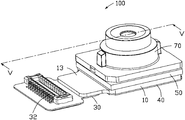
- FIG. 1 is an assembled, isometric view of an embodiment of a camera.
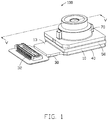
- FIG. 2 is similar to FIG. 1 , but shows the camera from another angle.
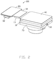
- FIG. 3 is an exploded view of the camera in FIG. 1 .
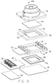
- FIG. 4 is an exploded view of the camera in FIG. 2 .
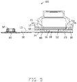
- FIG. 5 is a cross-sectional view of the camera in FIG. 1 taken along line V-V. please label “first carrier plate 40 ” to show 30 and 40 are arranged side by side).
- Coupled is defined as connected, whether directly or indirectly through intervening components, and is not necessarily limited to physical connections.
- the connection can be such that the objects are permanently connected or releasably connected.
- comprising means “including, but not necessarily limited to”; it specifically indicates open-ended inclusion or membership in a so-described combination, group, series and the like.
- FIGS. 1-5 show an embodiment of a camera 100 .
- the camera 100 includes a circuit board 10 , an image sensing chip 20 , a flexible circuit board 30 , a first carrier plate 40 , a package base 50 , a protecting cover 60 , a lens module 70 , and a second carrier plate 80 .
- the circuit board 10 may be made of ceramic or other hard material.
- the circuit board 10 includes a first surface 12 and a second surface 14 .
- the second surface 14 is opposite to the first surface 12 .
- the circuit board 10 defines a window 16 through the first surface 12 and the second surface 14 .
- the circuit board 10 further defines a mounting groove 18 .
- the mounting groove 18 is defined in the second surface 14 and is in communication with the second surface 14 .
- a size of the mounting groove 18 is greater than a size of the window 16 .
- the first surface 12 includes a plurality of circuit components 11 mounted around a periphery of the window 16 .
- the circuit components 11 may be, but are not limited to, resistors, capacitors, diodes, triodes, potentiometers, relays, drivers, or the like.
- the image sensing chip 20 is flip-chip mounted and received within the mounting groove 18 .
- the image sensing chip 20 is electrically coupled to the circuit components 11 to sense signals.
- the image sensing chip 20 includes a photosensitive area 22 facing the window 16 .
- the photosensitive area 22 is viewable through the window 16 and is capable of sensing light.
- the first carrier plate 40 is mounted to the second surface 14 and covers over the mounting groove 18 to seal the image sensing chip 20 to the side of the first carrier plate 40 facing the circuit board 10 .
- the first carrier plate 40 protects the image sensing chip 20 and prevents the image sensing chip 20 from falling out of the mounting groove 18 .
- the first carrier plate 40 is made of metal.
- the first carrier plate 40 is integrally formed with the circuit board 10 by a molding on board method.
- the circuit board 10 includes an end portion 13 .
- the end portion 13 is not covered by the first carrier plate 40 .
- the flexible circuit board 30 is mounted to the second surface 14 of the end portion 13 .
- the flexible circuit board 30 is electrically coupled to the image sensing chip 20 to provide signal transmission therebetween.
- the flexible circuit board 30 may be mounted to the end portion 13 by an adhesive, for example.
- the flexible circuit board 30 is electrically coupled to a connector 32 .
- the connector 32 provides signal transmission between the circuit board 10 and an external component.
- the second carrier plate 80 is mounted to a side of the flexible circuit board 30 facing away from the circuit board 10 and is adapted for protecting the flexible circuit board 30 .
- the second carrier plate 80 may be adhered to the flexible circuit board 30 by an adhesive, for example.
- the second carrier plate 80 is made of metal.
- the package base 50 is mounted to the second surface 12 of the circuit board 10 .
- the package base 50 is integrally formed with the circuit board 10 by a molding on board method.
- the package base 50 further covers over the plurality of circuit components 11 .
- the package base 50 defines a light hole 52 and a recessed area 54 .
- the recessed area 54 surrounds the light hold 52.
- the light hole 52 is located along a light path of the image sensing chip 20 .
- the package base 50 is made of non-transparent material capable of absorbing light scattered by lens elements of the lens module 70 .
- the package base 50 may be formed by injection molding, mold pressing, or the like. Material of the package base 50 may be selected from, but is not limited to, liquid crystal polymer and polypropylene. The mold pressing method may be carried out using resin.
- the package base 50 covers over the circuit components 11 , so that the circuit components 11 are not directly exposed to air, thereby preventing erosion of the circuit components 11 within the photosensitive area 22 .
- the package base 50 further includes a loading surface 56 facing away from the circuit board 10 .
- the protecting cover 60 is mounted within the recessed area 54 , and a surface of the protecting cover 60 facing away from the circuit board 10 when mounted in the recessed area 54 is not higher than the loading surface 56 .
- the protecting cover 60 is formed by a molding on board method.
- the lens module 70 is mounted to the loading surface 56 and aligned with the image sensing chip 20 . Light passing through the lens module 70 is first passed through the protecting cover 60 , and then received by the image sensing chip 20 .
- the protecting cover 60 is made of glass. In other embodiments, the protecting cover is made of resin. The protecting cover 60 may be an infrared filter to improve an image quality of the lens module 70 . In other embodiments, the protecting cover 60 is a transparent cover. The protecting cover 60 , the package base 50 , the circuit board 10 , and the first carrier plate 40 cooperatively protect the image sensing chip 20 . Thus, the photosensitive area 22 is protected from dust and debris.
- the lens module 70 may be a fixed-focus lens module or a variable-focus lens module.
- the flexible circuit board 30 and the first carrier plate 40 are both mounted to the second surface 14 in a side-by-side relationship, thereby decreasing a thickness of the camera 100 .
Landscapes
- Engineering & Computer Science (AREA)
- Physics & Mathematics (AREA)
- Microelectronics & Electronic Packaging (AREA)
- Signal Processing (AREA)
- Multimedia (AREA)
- General Physics & Mathematics (AREA)
- Optics & Photonics (AREA)
- Chemical & Material Sciences (AREA)
- Ceramic Engineering (AREA)
- Inorganic Chemistry (AREA)
- Health & Medical Sciences (AREA)
- Toxicology (AREA)
- Studio Devices (AREA)
- Solid State Image Pick-Up Elements (AREA)
- Transforming Light Signals Into Electric Signals (AREA)
Abstract
Description
Claims (12)
Applications Claiming Priority (3)
| Application Number | Priority Date | Filing Date | Title |
|---|---|---|---|
| CN201811014143.2 | 2018-08-31 | ||
| CN201811014143.2A CN110876002B (en) | 2018-08-31 | 2018-08-31 | camera |
| CN201811014143 | 2018-08-31 |
Publications (2)
| Publication Number | Publication Date |
|---|---|
| US20200077517A1 US20200077517A1 (en) | 2020-03-05 |
| US10856418B2 true US10856418B2 (en) | 2020-12-01 |
Family
ID=69640640
Family Applications (1)
| Application Number | Title | Priority Date | Filing Date |
|---|---|---|---|
| US16/182,567 Expired - Fee Related US10856418B2 (en) | 2018-08-31 | 2018-11-06 | Power supply for a camera |
Country Status (3)
| Country | Link |
|---|---|
| US (1) | US10856418B2 (en) |
| CN (1) | CN110876002B (en) |
| TW (1) | TW202011101A (en) |
Families Citing this family (4)
| Publication number | Priority date | Publication date | Assignee | Title |
|---|---|---|---|---|
| CN115118839B (en) * | 2021-03-17 | 2025-08-08 | 晋城三赢精密电子有限公司 | Camera modules and electronic devices |
| CN115706845B (en) * | 2021-08-10 | 2026-02-10 | 晋城三赢精密电子有限公司 | Lens module and electronic devices |
| WO2023036295A1 (en) * | 2021-09-10 | 2023-03-16 | 宁波舜宇光电信息有限公司 | Circuit board for camera module and corresponding camera module |
| WO2025108268A1 (en) * | 2023-11-21 | 2025-05-30 | 宁波舜宇光电信息有限公司 | Camera module and manufacturing method therefor |
Citations (6)
| Publication number | Priority date | Publication date | Assignee | Title |
|---|---|---|---|---|
| US20070252703A1 (en) * | 2006-04-26 | 2007-11-01 | Murata Manufacturing Co., Ltd. | Electromagnetic-coupling-module-attached article |
| US20100170082A1 (en) * | 2009-01-05 | 2010-07-08 | Primax Electronics Ltd. | Method for assembling image capturing device |
| US20140001496A1 (en) * | 2012-06-27 | 2014-01-02 | Flextronics Ap, Llc | Relampable led structure |
| CN105100569A (en) | 2015-07-28 | 2015-11-25 | 南昌欧菲光电技术有限公司 | Camera module and its first circuit board and second circuit board |
| US20180048796A1 (en) | 2016-08-10 | 2018-02-15 | Apple Inc. | Camera module with embedded components |
| CN108363159A (en) | 2017-01-26 | 2018-08-03 | 宁波舜宇光电信息有限公司 | One camera lens and camera module and its manufacturing method |
Family Cites Families (5)
| Publication number | Priority date | Publication date | Assignee | Title |
|---|---|---|---|---|
| US7734083B2 (en) * | 2005-07-08 | 2010-06-08 | Konica Minolta Opto, Inc. | Printed board, image pickup apparatus and camera |
| KR20070105723A (en) * | 2006-04-27 | 2007-10-31 | 삼성전기주식회사 | Camera module package |
| CN104796588B (en) * | 2015-03-10 | 2018-11-27 | 南昌欧菲光电技术有限公司 | camera module |
| CN206892433U (en) * | 2017-01-26 | 2018-01-16 | 宁波舜宇光电信息有限公司 | Camera lens and camera module |
| CN206742240U (en) * | 2017-04-28 | 2017-12-12 | 南昌欧菲光电技术有限公司 | Camera module and its photosensory assembly |
-
2018
- 2018-08-31 CN CN201811014143.2A patent/CN110876002B/en active Active
- 2018-09-20 TW TW107133243A patent/TW202011101A/en unknown
- 2018-11-06 US US16/182,567 patent/US10856418B2/en not_active Expired - Fee Related
Patent Citations (6)
| Publication number | Priority date | Publication date | Assignee | Title |
|---|---|---|---|---|
| US20070252703A1 (en) * | 2006-04-26 | 2007-11-01 | Murata Manufacturing Co., Ltd. | Electromagnetic-coupling-module-attached article |
| US20100170082A1 (en) * | 2009-01-05 | 2010-07-08 | Primax Electronics Ltd. | Method for assembling image capturing device |
| US20140001496A1 (en) * | 2012-06-27 | 2014-01-02 | Flextronics Ap, Llc | Relampable led structure |
| CN105100569A (en) | 2015-07-28 | 2015-11-25 | 南昌欧菲光电技术有限公司 | Camera module and its first circuit board and second circuit board |
| US20180048796A1 (en) | 2016-08-10 | 2018-02-15 | Apple Inc. | Camera module with embedded components |
| CN108363159A (en) | 2017-01-26 | 2018-08-03 | 宁波舜宇光电信息有限公司 | One camera lens and camera module and its manufacturing method |
Also Published As
| Publication number | Publication date |
|---|---|
| CN110876002B (en) | 2021-07-20 |
| US20200077517A1 (en) | 2020-03-05 |
| CN110876002A (en) | 2020-03-10 |
| TW202011101A (en) | 2020-03-16 |
Similar Documents
| Publication | Publication Date | Title |
|---|---|---|
| US7782390B2 (en) | Camera module | |
| US10856418B2 (en) | Power supply for a camera | |
| US7782391B2 (en) | Camera module having a structure for preventing external electronic waves and noise from being introduced into the camera module | |
| KR100673950B1 (en) | Image sensor module and camera module package with same | |
| US7643081B2 (en) | Digital camera module with small sized image sensor chip package | |
| US7638864B2 (en) | Chip package, method of making same and digital camera module using the package | |
| US7417810B2 (en) | Lens module with shielding layer | |
| US8482836B2 (en) | Flexible display device | |
| CN211555889U (en) | Image sensing module | |
| US10666843B2 (en) | Imaging chip packaging structure and camera device having the same | |
| US11297210B2 (en) | Camera module, method for assembling camera module, and mobile terminal | |
| US8203647B2 (en) | Image sensor module and method for manufacturing the same | |
| US20110267534A1 (en) | Image sensor package and camera module using same | |
| US20100025793A1 (en) | Assembly for image sensing chip and assembling method thereof | |
| US20200057228A1 (en) | Lens module and method of assembling lens module | |
| WO2021120954A1 (en) | Optical module, photosensitive module, camera module, and manufacturing method for optical module and photosensitive module | |
| CN104717407A (en) | Electronic device with camera dustproof assembly | |
| US20210021739A1 (en) | Lens module | |
| US11696009B2 (en) | Camera module and electronic device having the camera module | |
| KR100972440B1 (en) | Camera module | |
| US20190379811A1 (en) | Connection structure and camera module using same | |
| US11991429B2 (en) | Camera module | |
| TWI670802B (en) | Image sensor chip encapsulation structure and camera device | |
| KR101221511B1 (en) | Camera Module | |
| KR100935311B1 (en) | Wafer level camera module |
Legal Events
| Date | Code | Title | Description |
|---|---|---|---|
| AS | Assignment |
Owner name: TRIPLE WIN TECHNOLOGY(SHENZHEN) CO.LTD., CHINA Free format text: ASSIGNMENT OF ASSIGNORS INTEREST;ASSIGNORS:LI, KUN;CHEN, SHIN-WEN;LI, YU-SHUAI;AND OTHERS;REEL/FRAME:047427/0915 Effective date: 20181029 |
|
| FEPP | Fee payment procedure |
Free format text: ENTITY STATUS SET TO UNDISCOUNTED (ORIGINAL EVENT CODE: BIG.); ENTITY STATUS OF PATENT OWNER: LARGE ENTITY |
|
| STPP | Information on status: patent application and granting procedure in general |
Free format text: NON FINAL ACTION MAILED |
|
| STPP | Information on status: patent application and granting procedure in general |
Free format text: NOTICE OF ALLOWANCE MAILED -- APPLICATION RECEIVED IN OFFICE OF PUBLICATIONS |
|
| STPP | Information on status: patent application and granting procedure in general |
Free format text: PUBLICATIONS -- ISSUE FEE PAYMENT VERIFIED |
|
| STCF | Information on status: patent grant |
Free format text: PATENTED CASE |
|
| FEPP | Fee payment procedure |
Free format text: MAINTENANCE FEE REMINDER MAILED (ORIGINAL EVENT CODE: REM.); ENTITY STATUS OF PATENT OWNER: LARGE ENTITY |
|
| LAPS | Lapse for failure to pay maintenance fees |
Free format text: PATENT EXPIRED FOR FAILURE TO PAY MAINTENANCE FEES (ORIGINAL EVENT CODE: EXP.); ENTITY STATUS OF PATENT OWNER: LARGE ENTITY |
|
| STCH | Information on status: patent discontinuation |
Free format text: PATENT EXPIRED DUE TO NONPAYMENT OF MAINTENANCE FEES UNDER 37 CFR 1.362 |
|
| FP | Lapsed due to failure to pay maintenance fee |
Effective date: 20241201 |