US10855029B2 - Electrical connector assembly - Google Patents
Electrical connector assembly Download PDFInfo
- Publication number
- US10855029B2 US10855029B2 US16/705,465 US201916705465A US10855029B2 US 10855029 B2 US10855029 B2 US 10855029B2 US 201916705465 A US201916705465 A US 201916705465A US 10855029 B2 US10855029 B2 US 10855029B2
- Authority
- US
- United States
- Prior art keywords
- portions
- conducting
- substrate
- electrical connector
- contact
- Prior art date
- Legal status (The legal status is an assumption and is not a legal conclusion. Google has not performed a legal analysis and makes no representation as to the accuracy of the status listed.)
- Active
Links
- 239000000758 substrate Substances 0.000 claims abstract description 82
- 230000013011 mating Effects 0.000 claims abstract description 62
- 238000005452 bending Methods 0.000 claims description 28
- 239000002184 metal Substances 0.000 claims description 21
- 238000000034 method Methods 0.000 claims description 12
- 230000008569 process Effects 0.000 claims description 12
- 230000000903 blocking effect Effects 0.000 claims description 6
- 239000004020 conductor Substances 0.000 claims description 6
- 238000012986 modification Methods 0.000 description 4
- 230000004048 modification Effects 0.000 description 4
- 230000007246 mechanism Effects 0.000 description 3
- 229910000679 solder Inorganic materials 0.000 description 3
- 230000009286 beneficial effect Effects 0.000 description 2
- 230000008901 benefit Effects 0.000 description 1
- 230000007423 decrease Effects 0.000 description 1
- 230000007812 deficiency Effects 0.000 description 1
- 238000009432 framing Methods 0.000 description 1
- 230000017525 heat dissipation Effects 0.000 description 1
- 238000003780 insertion Methods 0.000 description 1
- 230000037431 insertion Effects 0.000 description 1
Images


Classifications
-
- H—ELECTRICITY
- H01—ELECTRIC ELEMENTS
- H01R—ELECTRICALLY-CONDUCTIVE CONNECTIONS; STRUCTURAL ASSOCIATIONS OF A PLURALITY OF MUTUALLY-INSULATED ELECTRICAL CONNECTING ELEMENTS; COUPLING DEVICES; CURRENT COLLECTORS
- H01R13/00—Details of coupling devices of the kinds covered by groups H01R12/70 or H01R24/00 - H01R33/00
- H01R13/62—Means for facilitating engagement or disengagement of coupling parts or for holding them in engagement
- H01R13/629—Additional means for facilitating engagement or disengagement of coupling parts, e.g. aligning or guiding means, levers, gas pressure electrical locking indicators, manufacturing tolerances
- H01R13/631—Additional means for facilitating engagement or disengagement of coupling parts, e.g. aligning or guiding means, levers, gas pressure electrical locking indicators, manufacturing tolerances for engagement only
-
- H—ELECTRICITY
- H01—ELECTRIC ELEMENTS
- H01R—ELECTRICALLY-CONDUCTIVE CONNECTIONS; STRUCTURAL ASSOCIATIONS OF A PLURALITY OF MUTUALLY-INSULATED ELECTRICAL CONNECTING ELEMENTS; COUPLING DEVICES; CURRENT COLLECTORS
- H01R12/00—Structural associations of a plurality of mutually-insulated electrical connecting elements, specially adapted for printed circuits, e.g. printed circuit boards [PCB], flat or ribbon cables, or like generally planar structures, e.g. terminal strips, terminal blocks; Coupling devices specially adapted for printed circuits, flat or ribbon cables, or like generally planar structures; Terminals specially adapted for contact with, or insertion into, printed circuits, flat or ribbon cables, or like generally planar structures
- H01R12/70—Coupling devices
- H01R12/71—Coupling devices for rigid printing circuits or like structures
- H01R12/72—Coupling devices for rigid printing circuits or like structures coupling with the edge of the rigid printed circuits or like structures
- H01R12/73—Coupling devices for rigid printing circuits or like structures coupling with the edge of the rigid printed circuits or like structures connecting to other rigid printed circuits or like structures
-
- H—ELECTRICITY
- H01—ELECTRIC ELEMENTS
- H01R—ELECTRICALLY-CONDUCTIVE CONNECTIONS; STRUCTURAL ASSOCIATIONS OF A PLURALITY OF MUTUALLY-INSULATED ELECTRICAL CONNECTING ELEMENTS; COUPLING DEVICES; CURRENT COLLECTORS
- H01R12/00—Structural associations of a plurality of mutually-insulated electrical connecting elements, specially adapted for printed circuits, e.g. printed circuit boards [PCB], flat or ribbon cables, or like generally planar structures, e.g. terminal strips, terminal blocks; Coupling devices specially adapted for printed circuits, flat or ribbon cables, or like generally planar structures; Terminals specially adapted for contact with, or insertion into, printed circuits, flat or ribbon cables, or like generally planar structures
- H01R12/50—Fixed connections
- H01R12/51—Fixed connections for rigid printed circuits or like structures
-
- H—ELECTRICITY
- H01—ELECTRIC ELEMENTS
- H01R—ELECTRICALLY-CONDUCTIVE CONNECTIONS; STRUCTURAL ASSOCIATIONS OF A PLURALITY OF MUTUALLY-INSULATED ELECTRICAL CONNECTING ELEMENTS; COUPLING DEVICES; CURRENT COLLECTORS
- H01R12/00—Structural associations of a plurality of mutually-insulated electrical connecting elements, specially adapted for printed circuits, e.g. printed circuit boards [PCB], flat or ribbon cables, or like generally planar structures, e.g. terminal strips, terminal blocks; Coupling devices specially adapted for printed circuits, flat or ribbon cables, or like generally planar structures; Terminals specially adapted for contact with, or insertion into, printed circuits, flat or ribbon cables, or like generally planar structures
- H01R12/70—Coupling devices
- H01R12/7082—Coupling device supported only by cooperation with PCB
-
- H—ELECTRICITY
- H01—ELECTRIC ELEMENTS
- H01R—ELECTRICALLY-CONDUCTIVE CONNECTIONS; STRUCTURAL ASSOCIATIONS OF A PLURALITY OF MUTUALLY-INSULATED ELECTRICAL CONNECTING ELEMENTS; COUPLING DEVICES; CURRENT COLLECTORS
- H01R12/00—Structural associations of a plurality of mutually-insulated electrical connecting elements, specially adapted for printed circuits, e.g. printed circuit boards [PCB], flat or ribbon cables, or like generally planar structures, e.g. terminal strips, terminal blocks; Coupling devices specially adapted for printed circuits, flat or ribbon cables, or like generally planar structures; Terminals specially adapted for contact with, or insertion into, printed circuits, flat or ribbon cables, or like generally planar structures
- H01R12/70—Coupling devices
- H01R12/71—Coupling devices for rigid printing circuits or like structures
- H01R12/712—Coupling devices for rigid printing circuits or like structures co-operating with the surface of the printed circuit or with a coupling device exclusively provided on the surface of the printed circuit
- H01R12/716—Coupling device provided on the PCB
-
- H—ELECTRICITY
- H01—ELECTRIC ELEMENTS
- H01R—ELECTRICALLY-CONDUCTIVE CONNECTIONS; STRUCTURAL ASSOCIATIONS OF A PLURALITY OF MUTUALLY-INSULATED ELECTRICAL CONNECTING ELEMENTS; COUPLING DEVICES; CURRENT COLLECTORS
- H01R12/00—Structural associations of a plurality of mutually-insulated electrical connecting elements, specially adapted for printed circuits, e.g. printed circuit boards [PCB], flat or ribbon cables, or like generally planar structures, e.g. terminal strips, terminal blocks; Coupling devices specially adapted for printed circuits, flat or ribbon cables, or like generally planar structures; Terminals specially adapted for contact with, or insertion into, printed circuits, flat or ribbon cables, or like generally planar structures
- H01R12/70—Coupling devices
- H01R12/82—Coupling devices connected with low or zero insertion force
-
- H—ELECTRICITY
- H01—ELECTRIC ELEMENTS
- H01R—ELECTRICALLY-CONDUCTIVE CONNECTIONS; STRUCTURAL ASSOCIATIONS OF A PLURALITY OF MUTUALLY-INSULATED ELECTRICAL CONNECTING ELEMENTS; COUPLING DEVICES; CURRENT COLLECTORS
- H01R13/00—Details of coupling devices of the kinds covered by groups H01R12/70 or H01R24/00 - H01R33/00
- H01R13/02—Contact members
- H01R13/10—Sockets for co-operation with pins or blades
- H01R13/11—Resilient sockets
- H01R13/112—Resilient sockets forked sockets having two legs
-
- H—ELECTRICITY
- H01—ELECTRIC ELEMENTS
- H01R—ELECTRICALLY-CONDUCTIVE CONNECTIONS; STRUCTURAL ASSOCIATIONS OF A PLURALITY OF MUTUALLY-INSULATED ELECTRICAL CONNECTING ELEMENTS; COUPLING DEVICES; CURRENT COLLECTORS
- H01R13/00—Details of coupling devices of the kinds covered by groups H01R12/70 or H01R24/00 - H01R33/00
- H01R13/46—Bases; Cases
- H01R13/502—Bases; Cases composed of different pieces
-
- H—ELECTRICITY
- H01—ELECTRIC ELEMENTS
- H01R—ELECTRICALLY-CONDUCTIVE CONNECTIONS; STRUCTURAL ASSOCIATIONS OF A PLURALITY OF MUTUALLY-INSULATED ELECTRICAL CONNECTING ELEMENTS; COUPLING DEVICES; CURRENT COLLECTORS
- H01R13/00—Details of coupling devices of the kinds covered by groups H01R12/70 or H01R24/00 - H01R33/00
- H01R13/62—Means for facilitating engagement or disengagement of coupling parts or for holding them in engagement
- H01R13/629—Additional means for facilitating engagement or disengagement of coupling parts, e.g. aligning or guiding means, levers, gas pressure electrical locking indicators, manufacturing tolerances
-
- H—ELECTRICITY
- H01—ELECTRIC ELEMENTS
- H01R—ELECTRICALLY-CONDUCTIVE CONNECTIONS; STRUCTURAL ASSOCIATIONS OF A PLURALITY OF MUTUALLY-INSULATED ELECTRICAL CONNECTING ELEMENTS; COUPLING DEVICES; CURRENT COLLECTORS
- H01R13/00—Details of coupling devices of the kinds covered by groups H01R12/70 or H01R24/00 - H01R33/00
- H01R13/62—Means for facilitating engagement or disengagement of coupling parts or for holding them in engagement
- H01R13/639—Additional means for holding or locking coupling parts together, after engagement, e.g. separate keylock, retainer strap
Definitions
- the present invention relates to an electrical connector, and in particular to an electrical connector assembly for electrically connecting a chip module to a circuit board.
- the Chinese patent No. CN201120155596.4 discloses an electrical connector for electrically connecting a chip module to a circuit board, including an electrical connection base, a cover capable of relatively sliding along the electrical connection base, and a driving mechanism for driving the cover to slide relative to the electrical connection base.
- the electrical connection base is provided with a circular base hole, and a top surface of the electrical connection base is provided with a conductive region.
- the conductive region is provided with multiple accommodating holes, and multiple terminals are respectively correspondingly accommodated in the accommodating holes.
- the cover slidably covers the electrical connection base, and one end thereof is provided with a perforation hole corresponding to the base hole.
- a top surface of the cover has a hollow portion corresponding to the conductive region, and the chip module is positioned in the hollow portion after being mounted into the electrical connector.
- the driving mechanism includes a rotary pin and a carrier. The rotary pin runs through the perforation hole and the base hole from top of the cover, and the carrier enters the base hole upward from bottom of the electrical connection base to match with the rotary pin. When the driving mechanism is rotated, the chip module moves together with the cover on the electrical connection base to realize electrical connection between the chip module and the circuit board.
- the chip module is pushed by a rear side surface (in which a moving direction of the chip module is a forward direction, and a direction opposite to the moving direction of the chip module is a backward direction) of the hollow portion to move.
- the rear side surface of the hollow portion is located at the rear side of a virtual center line of the hollow portion, such that the force received by the chip module to drive it to move forward is a pushing force, which easily causes warpage of the chip module during the movement.
- the present invention is directed to an electrical connector assembly that avoids warpage of the mating plug during the movement thereof.
- an electrical connector according to certain embodiments of the present invention adopts the following technical solutions:
- An electrical connector is configured to be electrically connected to a mating plug.
- the mating plug is provided with a substrate and a plurality of conducting portions protruding downward from the substrate, and the electrical connector includes: an insulating body; a plurality of terminals, respectively accommodated in the insulating body, wherein each of the terminals is provided with a contact portion; a cover, covering the insulating body in a front-rear sliding manner and having a hollow portion to accommodate the substrate, wherein the hollow portion has a virtual center line extending in a left-right direction, the cover is provided with a pulling portion to abut the substrate forward, and the pulling portion is located in front of the virtual center line; and a driving member, provided with a driving portion located in front of the hollow portion, wherein after the substrate of the mating plug is mounted downward into the hollow portion, the driving portion drives the cover to move horizontally forward relative to the insulating body, and the pulling portion pulls the substrate forward, such that the conducting portions move forward to be in contact with the contact
- a left side and a right side of the hollow portion are recessed to form a plurality of concave portions
- a left side and a right side of the substrate are provided with a plurality of protrusion portions correspondingly accommodated in the concave portions
- a rear side surface of each of the concave portions forms the pulling portion
- the pulling portion abuts the protrusion portions in front thereof.
- a rear side of the hollow portion forms an abutting portion, and when the cover moves horizontally forward, the abutting portion abuts a rear side of the substrate forward.
- a left side and a right side of the hollow portion are recessed to form a plurality of notches
- a left side and a right side of the substrate are provided with a plurality of projecting portions correspondingly accommodated in the notches
- a front side surface of each of the notches is located behind the virtual center line
- a rear side surface of each of the notches forms an abutting portion
- the abutting portion abuts the projecting portions located in front thereof.
- a left side and a right side of the hollow portion are recessed to form a plurality of recess portions, a front side surface of each of the recess portions is located in front of the virtual center line, a rear side surface of each of the recess portions is located behind the virtual center line, a left side and a right side of the substrate are provided with a plurality of projecting blocks correspondingly accommodated in the recess portions, the rear side surface of each of the recess portions forms an abutting portion, and when the cover moves horizontally forward, the abutting portion forward abuts the projecting blocks located in front thereof.
- a plurality of pressing sheets are located at two opposite sides of the hollow portion, each of the pressing sheets has a pivoting portion pivotally connected to the cover and a pressing portion extending from the pivoting portion, when the substrate is to be placed in the hollow portion, the pressing sheets are rotated such that the pressing portions thereof leave the hollow portion, and after the substrate is placed in the hollow portion, the pressing sheets are rotated such that the pressing portions thereof are pressed against an upper surface of the substrate.
- each of the terminals is provided with two contact portions provided opposite to each other in the left-right direction, the two contact portions extend backward and away from each other to form two guide portions, two of the terminals comprise a first terminal and a second terminal, after a respective conducting portion of the conducting portions is inserted downward between the two guide portions of a corresponding terminal of the terminals, a distance between each of the two contact portions of the first terminal and the respective conducting portion is less than a distance between each of the two contact portions of the second terminal and the respective conducting portion in a front-rear direction, and in a process of the respective conducting portion moving forward, the two contact portions of the first terminal clamp the respective conducting portion first, and then the two contact portions of the second terminal clamp the conducting portion.
- the electrical connector further includes a metal member, wherein the cover is made of metal and has a horizontal flat plate portion, and a plate edge of the flat plate portion is provided with a first slide track and a second slide track respectively extending in a front-rear direction; a plate edge of the metal member is provided with a first mating edge corresponding to a left side of the first slide track and a second mating edge corresponding to a right side of the second slide track, the first slide track abuts the first mating edge leftward, and the second slide track abuts the second mating edge rightward.
- the hollow portion is provided on the flat plate portion, the flat plate portion has a slide slot located behind the hollow portion, a right side of the slide slot forms the first slide track, and a left side of the slide slot forms the second slide track;
- the metal member has a bottom wall, the bottom wall is provided with an accommodating space to accommodate the insulating body, the bottom wall bends upward to form a rear bending portion located behind the accommodating space, the rear bending portion is accommodated in the slide slot, a right side of the rear bending portion forms the first mating edge, and a left side of the rear bending portion forms the second mating edge.
- the flat plate portion has a sliding block located in front of the hollow portion, a left side of the sliding block forms the first slide track, and a right side of the sliding block forms the second slide track;
- the bottom wall bends upward to form a front bending portion located in front of the accommodating space, the front bending portion is provided with a slot, the sliding block is accommodated in the slot, a left side of the slot forms the first mating edge, and a right side of the slot forms the second mating edge.
- the rear bending portion is provided with a through hole running through the rear bending portion in a front-rear direction, and the through hole has a top surface; and the cover is further provided with a protruding portion entering the through hole, such that the top surface of the through hole limits the cover from moving upward.
- the rear bending portion bends and extends backward to form an extending portion
- the flat plate portion is provided with a stopping surface located right below the extending portion to limit the cover from moving upward.
- a plurality of supporting portions protrude upward from the bottom wall, and the supporting portions support the flat plate portion upward, such that a gap is formed between the bottom wall and the flat plate portion in a vertical direction.
- the terminals are configured to be soldered to a circuit board, a back plate is located below the circuit board, the metal member is fixed to the back plate by a fixing member; a sleeve accommodates the driving member, the sleeve is provided with a fixing portion fixed in the circuit board, the fixing portion extends upward to form an upper portion accommodated in the metal member, and the fixing portion extends downward to form a lower portion accommodated in the back plate.
- an electrical connector assembly according to certain embodiments of the present invention adopts the following technical solutions:
- An electrical connector assembly includes: a mating plug, provided with a substrate and a plurality of conducting portions protruding downward from the substrate; and an electrical connector, including: an insulating body; a plurality of terminals, respectively accommodated in the insulating body, wherein each of the terminals is provided with a contact portion; a cover, covering the insulating body in a front-rear sliding manner and having a hollow portion to accommodate the substrate, wherein the hollow portion has a virtual center line extending in a left-right direction, the cover is provided with a pulling portion to abut the substrate forward, and the pulling portion is located in front of the virtual center line; and a driving member, provided with a driving portion located in front of the hollow portion, wherein after the substrate of the mating plug is mounted downward into the hollow portion, the driving portion drives the cover to move horizontally forward relative to the insulating body, and the pulling portion pulls the substrate forward, such that the conducting portions move forward to be in contact with the contact portions of the terminals.
- each of the terminals is provided with two contact portions provided opposite to each other in the left-right direction, the two contact portions extend backward and away from each other to form two guide portions, a front side of each of the conducting portions has an inclined surface, such that a width of each of the conducting portions gradually increases due to the inclined surface along a downward-from-top direction, after a respective conducting portion of the conducting portions is inserted downward between the two guide portions of a corresponding terminal of the terminals, the guide portions guide the respective conducting portion to move forward to the contact portions, and in a process of the respective conducting portion moving forward, the inclined surface of the respective conducting portion is in contact with the contact portions.
- each of the conducting portions has a mating surface for contacting the contact portion of a corresponding terminal of the terminals, and in a downward-from-top direction, the mating surface extends obliquely toward the contact portion of the corresponding terminal.
- a left side and a right side of each of the conducting portions are respectively provided with two blocking portions, and the guide portions or the contact portions of the corresponding terminal are buckled downward to the blocking portions of the respective conducting portion.
- an upper surface of the substrate has a plurality of conducting regions respectively correspondingly electrically connected to the conducting portions, the conducting regions are configured to be conductively connected to a plurality of electrical conductors of a chip module correspondingly, and a distance between two adjacent ones of the conducting portions is greater than a distance between two adjacent ones of the conducting regions.
- two of the conducting portions comprise a first conducting portion and a second conducting portion
- a width of the first conducting portion is greater than a width of the second conducting portion in a front-rear direction
- a distance between the first conducting portion and the contact portion of a corresponding terminal of the terminals is less than a distance between the second conducting portion and the contact portion of the corresponding terminal in the front-rear direction
- the first conducting portion is in contact with the contact portion of the corresponding terminal first
- the second conducting portion is in contact with the contact portion of the corresponding terminal.
- the pulling portion is provided in front of the virtual center line, and the pulling portion pulls the substrate forward. That is, the force received by the substrate to drive it to move forward is a pulling force, such that the warpage of the substrate during the moving of the mating plug can be avoided.
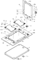
- FIG. 1 is a perspective exploded view of an electrical connector assembly according to a first embodiment of the present invention.
- FIG. 2 is a partial perspective exploded view of FIG. 1 .
- FIG. 3 is an exploded schematic view of a mating plug and a chip module according to the first embodiment of the present invention.
- FIG. 4 is a perspective view of the chip module and the mating plug before being assembled to the electrical connector according to the first embodiment of the present invention.
- FIG. 5 is a perspective view of the chip module and the mating plug after being assembled to the electrical connector according to the first embodiment of the present invention.
- FIG. 6 is a top view of FIG. 5 .
- FIG. 7 is a sectional view of FIG. 6 along line A-A.
- FIG. 8 is a partial enlarged view of FIG. 7 .
- FIG. 9 is an exploded schematic view of a conducting portion and a terminal according to the first embodiment of the present invention.
- FIG. 10 is a schematic view of the mating plug moving to the final position according to the first embodiment of the present invention.
- FIG. 11 is a sectional view of FIG. 10 along line B-B.
- FIG. 12 is a partial enlarged view of FIG. 11 .
- FIG. 13 is a schematic view of a conducting portion during moving and a terminal according to the first embodiment of the present invention.
- FIG. 14 is a schematic view of the conducting portion moving to the final position and clamped by the terminal according to the first embodiment of the present invention.
- FIG. 15 is a schematic view of the terminal clamping the conducting portion of FIG. 14 from another viewing angle.
- FIG. 16 is a top view of a metal member and an insulating body of the electrical connector after being assembled according to the first embodiment of the present invention.
- FIG. 17 is a top view of the conducting portion being inserted downward into the terminal according to the first embodiment of the present invention.
- FIG. 18 is a top view of the conducting portion horizontally moving to the final position and clamped by the terminal according to the first embodiment of the present invention.
- FIG. 19 is a schematic view of the mating plug being connected to the chip module according to the first embodiment of the present invention.
- FIG. 20 is a schematic view of a first terminal clamping the conducting portion first and then the second terminal clamping the conducting portion according to a second embodiment of the present invention.
- FIG. 21 is a schematic view of a first conducting portion being clamped by the terminal first and then a second conducting portion being clamped by the terminal according to a third embodiment of the present invention.
- FIG. 22 is an assembled view of an electrical connector assembly according to a fourth embodiment of the present invention.
- FIG. 23 is a top view of FIG. 22 .
- relative terms such as “lower” or “bottom” and “upper” or “top,” may be used herein to describe one element's relationship to another element as illustrated in the Figures. It will be understood that relative terms are intended to encompass different orientations of the device in addition to the orientation depicted in the Figures. For example, if the device in one of the figures is turned over, elements described as being on the “lower” side of other elements would then be oriented on “upper” sides of the other elements. The exemplary term “lower”, can therefore, encompasses both an orientation of “lower” and “upper,” depending of the particular orientation of the figure.
- “around”, “about” or “approximately” shall generally mean within 20 percent, preferably within 10 percent, and more preferably within 5 percent of a given value or range. Numerical quantities given herein are approximate, meaning that the term “around”, “about” or “approximately” can be inferred if not expressly stated.
- this invention in one aspect, relates to an electrical connector assembly.
- FIGS. 1-19 shows an electrical connector assembly according to a first embodiment of the present invention, including an electrical connector 200 and a mating plug 100 .
- the electrical connector 200 electrically connects the mating plug 100 to a circuit board 400 .
- the mating plug 100 includes a substrate 1 and multiple conducting portions 2 provided on the substrate 1 and protruding downward from the substrate 1 .
- a chip module 300 is supported on an upper surface of the substrate 1 and electrically connected to the substrate 1 .
- the electrical connector 200 includes an insulating body 4 ; multiple terminals 3 accommodated in the insulating body 4 ; a cover 5 covering the insulating body 4 and capable of horizontally moving in a front-rear direction relative to the insulating body 4 ; a driving member 7 driving the cover 5 to move horizontally in the front-rear direction; and a metal member 6 framing the insulating body 4 .
- the insulating body 4 is located on the circuit board 400 , and includes two body units 41 having the same structure.
- the two body units 41 are arranged side-by-side in the front-rear direction and along the same arranging direction.
- a recess 4121 is respectively recessed from each of a front side and a rear side of each of the body units 41 .
- the recess 4121 at the rear side of the body unit 41 at the front and the recess 4121 at the front side of the body unit 41 at the rear form a frame opening 412 altogether, such that the insulating body 4 has a hollow structure.
- the arrangement positions of the two body units 41 may be switchable, and the frame opening 412 defined after the switch remains unchanged.
- Multiple accommodating holes 411 run vertically through each of the body units 41 to accommodate the terminals 3 , and the terminals 3 accommodated in the accommodating holes 411 of the body unit 41 at the front and the terminals 3 accommodated in the accommodating holes 411 of the body unit 41 at the rear are arranged in the same direction.
- each terminal 3 has a base 31 having a flat plate shape.
- a plate surface of the base 31 is perpendicular to the front-rear direction.
- the base 31 extends upward to form two elastic portions 34 , and the two elastic portions 34 and the base 31 are located on the same plane.
- Each of the elastic portions 34 bends and extends forward to form a guide portion 33 , and the guide portion 33 bends and extends forward to form a contact portion 32 .
- a distance between the two guide portions 33 of each terminal 3 is greater than a distance between the two contact portions 32 .
- Each of the elastic portions 34 has a first portion 341 connected to the base 31 and a second portion 342 extending upward from the first portion 341 to be connected to the guide portion 33 .
- a distance between the two second portions 342 of each terminal 3 is identical, and a distance between the two first portions 341 of each terminal 3 gradually decreases from the base 31 toward the second portion 342 .
- the base 31 bends downward and forward and then bends backward to form a position limiting portion 35 abutting an inner wall of the accommodating hole 411 downward to limit the terminal 3 from moving downward.
- the position limiting portion 35 protrudes from a front side and a rear side of the base 31 .
- a left side and a right side of the base 31 bend and extend forward to form two clamping arms 36 to clamp a solder e, and the solder e is used to be soldered to the circuit board 400 (as shown in FIGS. 7 and 8 ).
- the substrate 1 is located above the insulating body 4 , and has a multi-layered printed circuit 12 between an upper surface and a lower surface thereof.
- a left side and a right side of the substrate 1 are respectively provided with two protrusion portions 11 , and the upper surface of the substrate 1 further has multiple conducting regions 13 .
- the chip module 300 has multiple electrical conductors c correspondingly conducted to the conducting region 13 respectively.
- the electrical conductor c is a solder ball.
- the chip module 300 may not be soldered on the substrate 1 , and the chip module 300 may be crimped on the substrate 1 .
- a thickness of each conducting portion 2 in a left-right direction is less than the minimum distance between the two guide portions 33 of each of the terminals 3 , such that the conducting portion 2 is inserted between the two guide portions 33 with zero insertion force.
- the conducting region 13 is correspondingly electrically connected to the conducting portion 2 through the multi-layered printed circuit 12 , such that each of the electrical conductors c is electrically conductively connected to the corresponding conducting portion 2 .
- a distance M between two adjacent conducting portions 2 is greater than a distance N between two adjacent conducting regions 13 , such that there is sufficient space for providing the terminals 3 having the same quantity as that of the electrical conductors c. As shown in FIGS.
- each conducting portion 2 has an inclined surface 21 , and the inclined surface 21 gradually increases the width of the conducting portion 2 in a downward-from-top direction.
- the guide portions 33 guide the conducting portion 2 to move forward to the contact portions 32 .
- the inclined surface 21 is in contact with the contact portions 32 , and a downward component force F 1 is formed to act on the inclined surface 21 , such that the mating plug 100 is prevented from floating upward. As shown in FIG.
- a left side and a right side of the conducting portion 2 are respectively provided with two grooves 22 , the contact portions 32 clamp the grooves 22 , and each groove 22 has a mating surface 221 to be in contact with the corresponding contact portion 32 .
- the mating surface 221 extends obliquely toward the corresponding contact portion 32 . That is, in the downward-from-top direction, the two mating surfaces 221 of each of the conducting portions 2 are gradually separated from each other.
- a downward component force is formed to act on the mating surface 221 to further prevent the mating plug 100 from floating upward.
- a lower end of each groove 22 forms a blocking portion 23 .
- the guide portions 33 or the contact portions 32 are buckled downward to the blocking portions 23 to prevent the mating plug 100 from moving upward.
- the cover 5 is made of metal, and the cover 5 has a flat plate portion 51 .
- the flat plate portion 51 is provided with a hollow portion 511 which runs through an upper surface and a lower surface thereof to accommodate the substrate 1 , and the hollow portion 511 has a virtual center line extending along a left-right direction.
- a plate edge of the flat plate portion 51 is provided with two first slide tracks 50 a and two second slide tracks 50 b extending in the front-rear direction, and the flat plate portion 51 has a slide slot 512 located behind the hollow portion 511 .
- the flat plate portion 51 is provided with a sliding block 52 located in front of the hollow portion 511 .
- the other first slide track 50 a is provided on a left side of the sliding block 52
- the other second slide track 50 b is provided on a right side of the sliding block 52 .
- the flat plate portion 51 is respectively provided with two pulling portions 54 at a left side and a right side of the hollow portion 511 , and the pulling portion 54 is located in front of the virtual center line L of the hollow portion 511 .
- a left side surface and a right side surface of the hollow portion 511 are respectively recessed to form two concave portions 55 , and each of the concave portions 55 correspondingly accommodates each of the protrusion portions 11 .
- a front side of the concave portion 55 forms the pulling portion 54 , and the pulling portion 54 abuts a rear side surface of the protrusion portions 11 in front thereof.
- a rear side surface of the hollow portion 511 forms a first abutting portion 58 a abutting a rear side of the substrate 1 .
- a first stopping position 59 a and a second stopping position 59 b are soldered to an upper surface of the cover 5 . In other embodiments, the first stopping position 59 a and the second stopping position 59 b may also be integrally formed with the cover 5 .
- a front side and a rear side of the hollow portion 511 are respectively provided with two pressing sheets 8 .
- the front and rear sides of the hollow portion 511 may also be respectively provided with one pressing sheet 8 , or the pressing sheets 8 may also be provided on the left and right sides of the hollow portion 511 .
- Each pressing sheet 8 is made of metal, and has a pivoting portion 81 .
- a rivet g is fixed to the cover 5 , and the pivoting portion 81 is pivotally connected to the rivet g such that the pivoting portion 81 is pivotally connected to the cover 5 .
- the pressing sheet 8 may also be directly pivotally connected to the cover 5 .
- a pressing portion 82 extends from the pivoting portion 81 .
- the pressing sheets 8 are rotated such that the pressing portions 82 leave the hollow portion 511 , and after the substrate 1 is placed in the hollow portion 511 , the pressing sheets 81 are rotated such that the pressing portions 82 are pressed against an upper surface of the substrate 1 .
- the metal member 6 has a bottom wall 61 , and four screws run downward through the bottom wall 61 to fix the bottom wall 61 to a back plate d.
- the back plate d is located on a lower surface of the circuit board 400 .
- the bottom wall 61 is provided with an accommodating space 66 , and the two body units 41 are provided side-by-side in the accommodating space 66 .
- a plate edge of the metal member 6 is provided with two first mating edges 60 a corresponding to the left sides of the two first slide tracks 50 a and two second mating edges 60 b corresponding to the right sides of the second slide tracks 50 b .
- the first slide tracks 50 a abut the first mating edge 60 a leftward, and the second slide tracks 50 b abut the second mating edge 60 b rightward to prevent the cover 5 from deviating leftward or rightward during the front-rear sliding.
- a front side of the bottom wall 61 bends upward to form a front bending portion 62 located in front of the accommodating space 66 .
- the front bending portion 62 is provided with a slot 621 , and the slot 621 divides the front bending portion 62 into two portions side-by-side in a left-right direction.
- the sliding block 52 is accommodated in the slot 621 .
- a left side of the slot 621 forms one of the first mating edges 60 a corresponding to the first slide track 50 a formed on the left side of the sliding block 52
- a right side of the slot 621 forms one of the second mating edges 60 b corresponding to the second slide track 50 b formed on the right side of the sliding block 52
- the bottom wall 61 bends upward to form a rear bending portion 63 located behind the accommodating space 66 .
- the rear bending portion 63 is accommodated in the slide slot 512 .
- a right side of the rear bending portion 63 forms the other first mating edge 60 a corresponding to the first slide track 50 a formed on the right side of the slide slot 512
- the left side of the rear bending portion 63 forms the other second mating edge 60 b corresponding to the second slide track 50 b formed on the left side of the slide slot 512
- the rear bending portion 63 bends and extends backward to form an extending portion 64
- the flat plate portion 51 is provided with a stopping surface 513 located right below the extending portion 64 to limit the cover 5 from moving upward.
- each supporting portion 65 protrude upward from the bottom wall 61 , and the supporting portions 65 support the flat plate portion 51 upward, such that a gap is formed between the bottom wall 61 and the flat plate portion 51 in a vertical direction for heat dissipation.
- each supporting portion 65 is in a cylindrical shape.
- the driving member 7 is a cam made of metal, and is located in front of the hollow portion 511 .
- the driving member 7 has a head portion 71 abutting the upper surface of the cover 5 , and a protruding block 72 extending outward from the head portion 71 .
- the protruding block 72 rotates horizontally between the first stopping position 59 a and the second stopping position 59 b .
- a driving portion 73 extends downward from the head portion 71 and is accommodated in the cover 5 .
- a column 74 extends downward from the driving portion 73 and is accommodated in the metal member 6 .
- the center of the driving portion 73 is offset from the center of the head portion 71 and the column 74 .
- a portion of the column 74 protruding from the back plate d is provided with a clamping slot (not shown) to be fastened with a clamping ring f to prevent the driving member 7 from moving upward.
- a sleeve 9 accommodates the driving member 7 .
- the sleeve 9 is made of metal, and is provided with a fixing portion 91 fixed in the circuit board 400 .
- the fixing portion 91 extends upward to form an upper portion 92 accommodated in the bottom wall 61 , and the fixing portion 91 extends downward to form a lower portion 93 accommodated in the back plate d.
- the driving portion 73 abuts the cover 5 forward and the pulling portion 54 pulls the substrate 1 , such that the cover 5 moves horizontally forward altogether with the substrate 1 , so as to drive the conducting portions 2 to move forward from the guide portions 33 to the contact portions 32 .
- the driving portion 73 abuts the cover 5 backward to drive the substrate 1 to move horizontally backward, such that the conducting portions 2 are driven to move from the contact portions 32 to the guide portions 33 .
- each conducting portion 2 is separated from the contact portions 32 .
- FIG. 20 shows a second embodiment of the present invention, which is different from the first embodiment in that the terminals 3 include a first terminal 3 a and a second terminal 3 b , and the first terminal 3 a is a ground terminal.
- the first terminal 3 a is a power terminal, or multiple first terminals 3 a are provided, including a ground terminal and a power terminal.
- the first terminal 3 a and the second terminal 3 b have different structures.
- a distance between the two contact portions 32 of the first terminal 3 a and the corresponding conducting portion 2 is less than a distance between the two contact portions 32 of the second terminal 3 b and the corresponding conducting portion 2 .
- the first terminal 3 a clamps the conducting portion 2 first and then the second terminal 3 b clamps the conducting portion 2 .
- Other structures and functions of this embodiment are completely identical to those in the first embodiment, and thus are not further elaborated herein.
- FIG. 21 shows a third embodiment of the present invention, which is different from the first embodiment in that the conducting portions 2 include a first conducting portion 2 a and a second conducting portion 2 b .
- a width of the first conducting portion 2 a in the front-rear direction is greater than a width of the second conducting portion 2 b in the front-rear direction.
- the first conducting portion 2 a is in contact with the contact portions 32 of the corresponding terminal 3 first and then the second conducting portion 2 b is in contact with the contact portions 32 of the corresponding terminal 3 .
- the terminal 3 for clamping the first conducting portion 2 a is a ground terminal.
- the terminal 3 may be a power terminal, or multiple terminals 3 are provided for clamping the first conducting portion 2 a , including a ground terminal and a power terminal.
- Other structures and functions of this embodiment are completely identical to those in the first embodiment, and thus are not further elaborated herein.
- FIGS. 22 and 23 show a fourth embodiment of the present invention, which is different from the first embodiment in that the cover 5 further has two second abutting portions 58 b and two third abutting portions 58 c , which are all located behind the virtual center line L of the hollow portion 511 .
- the left and right sides of the hollow portion 511 are respectively recessed to form two notches 56 .
- the left and right sides of the substrate 1 are respectively provided with two projecting portions 14 respectively accommodated in the notches 56 .
- a rear side surface of each notch 56 forms the second abutting portion 58 b which abuts the projecting portions 14 located in front thereof.
- the left and right sides of the hollow portion 511 are respectively recessed to form two recess portions 57 .
- each recess portion 57 is located at the front side of the virtual center line L, and a rear side surface of each recess portion 57 is located at the rear side of the virtual center line L.
- the left and right sides of the substrate 1 are provided with two projecting blocks 15 respectively accommodated in the recess portions 57 , and a rear side surface of each recess portion 57 forms the third abutting portion 58 c which forward abuts the projecting blocks 15 located in front thereof.
- the pulling portion 54 pulls the substrate 1 to move horizontally forward, and the first abutting portions 58 a , the second abutting portions 58 b and the third abutting portions 58 c push the substrate 1 to move horizontally forward altogether, so as to drive the conducting portion 2 to move from the guide portions 33 to be clamped by the contact portions 32 of the corresponding terminal 3 .
- the protruding block 72 horizontally rotates from the first stopping position 59 a toward the second stopping position 59 b in a different direction. That is, the rotating direction thereof is clockwise in the first embodiment, and counterclockwise in this embodiment.
- an angle at which the protruding block 72 horizontally rotates from the first stopping position 59 a toward the second stopping position 59 b is greater than 180°, such that the driving member 7 drives the cover 5 more easily.
- the rear bending portion 63 is provided with a through hole 631 running through the rear bending portion 63 in the front-rear direction, and the through hole 631 has a top surface.
- a protruding portion 53 extends backward from one side of the slide slot 512 .
- the protruding portion 53 is located between the left side and the right side of the slide slot 512 , and the protruding portion 53 enters the through hole 631 , such that the top surface of the through hole 631 limits the cover 5 from moving upward.
- the substrate 1 is provided with multiple supporting columns h for supporting a heat sink (not shown).
- the pressing portion 82 is provided with a bump 821 protruding downward, and the bump 821 abuts the substrate 1 downward.
- Other structures and functions of this embodiment are completely identical to those in the first embodiment, and thus are not further elaborated herein.
- the electrical connector assembly 200 has the following beneficial effects:
- the pulling portion 54 is provided in front of the virtual center line L, and the pulling portion 54 pulls the substrate 1 forward. That is, the force received by the substrate 1 to drive it to move forward is a pulling force, such that the warpage of the substrate 1 during the moving of the mating plug 100 can be avoided.
- a pulling force from the pulling portion 54 acts on the substrate 1 in front of the virtual center line L and a pushing force from the first abutting portions 58 a , the second abutting portions 58 b or the third abutting portion 58 c acts on the substrate 1 behind the virtual center line L, so as to jointly push the substrate 1 to move horizontally forward.
- the force acting on the substrate 1 is more uniform during the forward moving process, and the warpage of the substrate 1 during the movement can be avoided.
- the distance between the two contact portions 32 of the first terminal 3 a and the conducting portion 2 is less than the distance between the two contact portions 32 of the second terminal 3 b and the conducting portion 2 in the front-rear direction.
- the two contact portions 32 of the first terminal 3 a clamp the conducting portion 2 first, and then the two contact portions 32 of the second terminal 3 b clamp the conducting portion 2 , such that the force when the conducting portion 2 is in contact with the contact portion 32 is dispersed, thereby reducing the driving force required for driving the cover 5 by the driving member 7 .
- the width of the first conducting portion 2 a is greater than the width of the second conducting portion 2 b in the front-rear direction.
- the first conducting portion 2 a is clamped by the terminal 3 first, and then the second conducting portion 2 b is clamped by the terminal 3 , such that the force when the conducting portion 2 is in contact with the contact portion 32 is dispersed, thereby reducing the driving force required for driving the cover 5 by the driving member 7 .
- the plate edge of the flat plate portion 51 is provided with a first slide track 50 a and a second slide track 50 b respectively extending in the front-rear direction.
- the first slide track 50 a abuts the first mating edge 60 a leftward
- the second slide track 50 b abuts the second mating edge 60 b rightward.
- the size can be more precise and the left and right offset of the cover 5 can be reduced since the first slide track 50 a and the second slide track 50 b are formed by the plate edge of the flat plate portion 51 .
- the mating plug 100 moves horizontally forward more stably, so as to ensure good connection between the conducting portion 2 and the terminal 3 .
Landscapes
- Coupling Device And Connection With Printed Circuit (AREA)
Priority Applications (1)
| Application Number | Priority Date | Filing Date | Title |
|---|---|---|---|
| US16/705,465 US10855029B2 (en) | 2018-12-10 | 2019-12-06 | Electrical connector assembly |
Applications Claiming Priority (5)
| Application Number | Priority Date | Filing Date | Title |
|---|---|---|---|
| US201862777312P | 2018-12-10 | 2018-12-10 | |
| CN201910815500 | 2019-08-30 | ||
| CN201910815500.3A CN110611183B (zh) | 2018-12-10 | 2019-08-30 | 电连接器 |
| CN201910815500.3 | 2019-08-30 | ||
| US16/705,465 US10855029B2 (en) | 2018-12-10 | 2019-12-06 | Electrical connector assembly |
Publications (2)
| Publication Number | Publication Date |
|---|---|
| US20200185859A1 US20200185859A1 (en) | 2020-06-11 |
| US10855029B2 true US10855029B2 (en) | 2020-12-01 |
Family
ID=68890743
Family Applications (1)
| Application Number | Title | Priority Date | Filing Date |
|---|---|---|---|
| US16/705,465 Active US10855029B2 (en) | 2018-12-10 | 2019-12-06 | Electrical connector assembly |
Country Status (2)
| Country | Link |
|---|---|
| US (1) | US10855029B2 (zh) |
| CN (2) | CN110611183B (zh) |
Citations (9)
| Publication number | Priority date | Publication date | Assignee | Title |
|---|---|---|---|---|
| CN2407463Y (zh) | 1999-12-01 | 2000-11-22 | 宣得股份有限公司 | 电连接器 |
| US6716051B1 (en) * | 2002-10-18 | 2004-04-06 | Hon Hai Precision Ind. Co., Ltd. | Electrical connector with distortion-resistant cover |
| US20100087081A1 (en) * | 2008-10-07 | 2010-04-08 | Hon Hai Precision Industry Co., Ltd. | Zif socket having reinforced cover preventing breakage during maneuvering |
| US20100190370A1 (en) * | 2009-01-20 | 2010-07-29 | Hon Hai Precision Ind. Co., Ltd. | Ic socket with offset cam capable of preventing warpage of cover |
| US20110076870A1 (en) * | 2009-09-30 | 2011-03-31 | Hon Hai Precision Industry Co., Ltd. | Electrical connector having improved base plate to support cam |
| US7918681B2 (en) * | 2009-07-08 | 2011-04-05 | Lotes Co., Ltd. | Electrical connector |
| US20110104928A1 (en) * | 2009-11-02 | 2011-05-05 | Hon Hai Precision Industry Co., Ltd. | Electrical connector with improved cam actuator |
| CN202068000U (zh) | 2011-05-12 | 2011-12-07 | 番禺得意精密电子工业有限公司 | 电连接器 |
| US8734177B2 (en) * | 2012-09-11 | 2014-05-27 | Lotes Co., Ltd. | Electrical connector assembly for securing chip module |
Family Cites Families (8)
| Publication number | Priority date | Publication date | Assignee | Title |
|---|---|---|---|---|
| CN2697875Y (zh) * | 2004-03-26 | 2005-05-04 | 富士康(昆山)电脑接插件有限公司 | 电连接器 |
| CN2708532Y (zh) * | 2004-05-18 | 2005-07-06 | 番禺得意精密电子工业有限公司 | 电连接器 |
| JP2006253348A (ja) * | 2005-03-10 | 2006-09-21 | Tyco Electronics Amp Kk | Icパッケージ、icソケットおよびicソケット組立体 |
| CN2932755Y (zh) * | 2006-06-06 | 2007-08-08 | 富士康(昆山)电脑接插件有限公司 | 电连接器 |
| CN201199568Y (zh) * | 2007-12-20 | 2009-02-25 | 番禺得意精密电子工业有限公司 | 电连接器 |
| CN201369431Y (zh) * | 2009-03-18 | 2009-12-23 | 番禺得意精密电子工业有限公司 | 电连接器 |
| CN201781097U (zh) * | 2010-07-22 | 2011-03-30 | 番禺得意精密电子工业有限公司 | 电连接器 |
| CN204291631U (zh) * | 2014-12-31 | 2015-04-22 | 深圳雷柏科技股份有限公司 | 用于波峰焊的pcb板治具及波峰焊治具拆卸装置 |
-
2019
- 2019-08-30 CN CN201910815500.3A patent/CN110611183B/zh active Active
- 2019-08-30 CN CN201910813639.4A patent/CN110611185B/zh active Active
- 2019-12-06 US US16/705,465 patent/US10855029B2/en active Active
Patent Citations (9)
| Publication number | Priority date | Publication date | Assignee | Title |
|---|---|---|---|---|
| CN2407463Y (zh) | 1999-12-01 | 2000-11-22 | 宣得股份有限公司 | 电连接器 |
| US6716051B1 (en) * | 2002-10-18 | 2004-04-06 | Hon Hai Precision Ind. Co., Ltd. | Electrical connector with distortion-resistant cover |
| US20100087081A1 (en) * | 2008-10-07 | 2010-04-08 | Hon Hai Precision Industry Co., Ltd. | Zif socket having reinforced cover preventing breakage during maneuvering |
| US20100190370A1 (en) * | 2009-01-20 | 2010-07-29 | Hon Hai Precision Ind. Co., Ltd. | Ic socket with offset cam capable of preventing warpage of cover |
| US7918681B2 (en) * | 2009-07-08 | 2011-04-05 | Lotes Co., Ltd. | Electrical connector |
| US20110076870A1 (en) * | 2009-09-30 | 2011-03-31 | Hon Hai Precision Industry Co., Ltd. | Electrical connector having improved base plate to support cam |
| US20110104928A1 (en) * | 2009-11-02 | 2011-05-05 | Hon Hai Precision Industry Co., Ltd. | Electrical connector with improved cam actuator |
| CN202068000U (zh) | 2011-05-12 | 2011-12-07 | 番禺得意精密电子工业有限公司 | 电连接器 |
| US8734177B2 (en) * | 2012-09-11 | 2014-05-27 | Lotes Co., Ltd. | Electrical connector assembly for securing chip module |
Also Published As
| Publication number | Publication date |
|---|---|
| CN110611183A (zh) | 2019-12-24 |
| CN110611185B (zh) | 2021-01-26 |
| CN110611185A (zh) | 2019-12-24 |
| CN110611183B (zh) | 2021-03-16 |
| US20200185859A1 (en) | 2020-06-11 |
Similar Documents
| Publication | Publication Date | Title |
|---|---|---|
| US10601162B2 (en) | Electrical connector | |
| US9954312B1 (en) | Electrical connector | |
| US10148024B2 (en) | Electrical connector with dual electrical path | |
| US10135199B1 (en) | Electrical connector | |
| US20200328550A1 (en) | Electrical connector | |
| US8475000B2 (en) | Connector, and LED lighting apparatus using the connector | |
| US9142905B2 (en) | Receptacle connector with high retention force | |
| US10601157B2 (en) | Electrical connector | |
| US10784606B2 (en) | Electrical connector and connector assembly | |
| US8545250B2 (en) | Electrical connector for connecting chip module to circuit board | |
| US20210344142A1 (en) | Plug connector and connector assembly having the same | |
| US7165991B2 (en) | Connector | |
| US11217919B2 (en) | Electrical connector with recessed opening for accommodating increased elastic arm length | |
| US20230070662A1 (en) | Electrical connector and method of manufacturing the same | |
| US7878846B2 (en) | Stacked electrical connectors on opposite sides of a printed circuit board | |
| US11309646B2 (en) | Electrical connector having terminals with reduced height | |
| US11011862B2 (en) | Electrical connector | |
| US10855029B2 (en) | Electrical connector assembly | |
| US8221136B2 (en) | Electrical connector with two connector bodies mounted on opposite surfaces of a PCB | |
| US7588453B2 (en) | Zero insertion force connector with improved driving device | |
| US10211549B2 (en) | Electrical connector | |
| US20130157518A1 (en) | Electrical connector | |
| US10547130B2 (en) | Electrical connector having protruding portions on metal shell | |
| US10714855B2 (en) | Electrical connector | |
| US9893445B1 (en) | Connector assembly |
Legal Events
| Date | Code | Title | Description |
|---|---|---|---|
| AS | Assignment |
Owner name: LOTES CO., LTD, TAIWAN Free format text: ASSIGNMENT OF ASSIGNORS INTEREST;ASSIGNOR:JIN, ZUO FENG;REEL/FRAME:051199/0624 Effective date: 20191202 |
|
| FEPP | Fee payment procedure |
Free format text: ENTITY STATUS SET TO UNDISCOUNTED (ORIGINAL EVENT CODE: BIG.); ENTITY STATUS OF PATENT OWNER: LARGE ENTITY |
|
| STPP | Information on status: patent application and granting procedure in general |
Free format text: NOTICE OF ALLOWANCE MAILED -- APPLICATION RECEIVED IN OFFICE OF PUBLICATIONS |
|
| STPP | Information on status: patent application and granting procedure in general |
Free format text: PUBLICATIONS -- ISSUE FEE PAYMENT RECEIVED |
|
| STCF | Information on status: patent grant |
Free format text: PATENTED CASE |
|
| MAFP | Maintenance fee payment |
Free format text: PAYMENT OF MAINTENANCE FEE, 4TH YEAR, LARGE ENTITY (ORIGINAL EVENT CODE: M1551); ENTITY STATUS OF PATENT OWNER: LARGE ENTITY Year of fee payment: 4 |