US10819293B2 - Power amplifier - Google Patents

Power amplifier Download PDF

Info

Publication number
US10819293B2
US10819293B2 US16/383,818 US201916383818A US10819293B2 US 10819293 B2 US10819293 B2 US 10819293B2 US 201916383818 A US201916383818 A US 201916383818A US 10819293 B2 US10819293 B2 US 10819293B2
Authority
US
United States
Prior art keywords
output
amplifier
power supply
voltage
input unit
Prior art date
Legal status (The legal status is an assumption and is not a legal conclusion. Google has not performed a legal analysis and makes no representation as to the accuracy of the status listed.)
Active, expires
Application number
US16/383,818
Other versions
US20190245494A1 (en
Inventor
Yohei OHTANI
Current Assignee (The listed assignees may be inaccurate. Google has not performed a legal analysis and makes no representation or warranty as to the accuracy of the list.)
Yamaha Corp
Original Assignee
Yamaha Corp
Priority date (The priority date is an assumption and is not a legal conclusion. Google has not performed a legal analysis and makes no representation as to the accuracy of the date listed.)
Filing date
Publication date
Application filed by Yamaha Corp filed Critical Yamaha Corp
Assigned to YAMAHA CORPORATION reassignment YAMAHA CORPORATION ASSIGNMENT OF ASSIGNORS INTEREST (SEE DOCUMENT FOR DETAILS). Assignors: OHTANI, Yohei
Publication of US20190245494A1 publication Critical patent/US20190245494A1/en
Application granted granted Critical
Publication of US10819293B2 publication Critical patent/US10819293B2/en
Active legal-status Critical Current
Adjusted expiration legal-status Critical

Links

Images

Classifications

    • HELECTRICITY
    • H03ELECTRONIC CIRCUITRY
    • H03FAMPLIFIERS
    • H03F1/00Details of amplifiers with only discharge tubes, only semiconductor devices or only unspecified devices as amplifying elements
    • H03F1/34Negative-feedback-circuit arrangements with or without positive feedback
    • HELECTRICITY
    • H03ELECTRONIC CIRCUITRY
    • H03FAMPLIFIERS
    • H03F3/00Amplifiers with only discharge tubes or only semiconductor devices as amplifying elements
    • H03F3/181Low-frequency amplifiers, e.g. audio preamplifiers
    • H03F3/183Low-frequency amplifiers, e.g. audio preamplifiers with semiconductor devices only
    • H03F3/187Low-frequency amplifiers, e.g. audio preamplifiers with semiconductor devices only in integrated circuits
    • HELECTRICITY
    • H03ELECTRONIC CIRCUITRY
    • H03FAMPLIFIERS
    • H03F3/00Amplifiers with only discharge tubes or only semiconductor devices as amplifying elements
    • H03F3/20Power amplifiers, e.g. Class B amplifiers, Class C amplifiers
    • H03F3/21Power amplifiers, e.g. Class B amplifiers, Class C amplifiers with semiconductor devices only
    • H03F3/211Power amplifiers, e.g. Class B amplifiers, Class C amplifiers with semiconductor devices only using a combination of several amplifiers
    • HELECTRICITY
    • H03ELECTRONIC CIRCUITRY
    • H03FAMPLIFIERS
    • H03F3/00Amplifiers with only discharge tubes or only semiconductor devices as amplifying elements
    • H03F3/20Power amplifiers, e.g. Class B amplifiers, Class C amplifiers
    • H03F3/21Power amplifiers, e.g. Class B amplifiers, Class C amplifiers with semiconductor devices only
    • H03F3/217Class D power amplifiers; Switching amplifiers
    • H03F3/2171Class D power amplifiers; Switching amplifiers with field-effect devices
    • HELECTRICITY
    • H03ELECTRONIC CIRCUITRY
    • H03FAMPLIFIERS
    • H03F3/00Amplifiers with only discharge tubes or only semiconductor devices as amplifying elements
    • H03F3/20Power amplifiers, e.g. Class B amplifiers, Class C amplifiers
    • H03F3/21Power amplifiers, e.g. Class B amplifiers, Class C amplifiers with semiconductor devices only
    • H03F3/217Class D power amplifiers; Switching amplifiers
    • H03F3/2178Class D power amplifiers; Switching amplifiers using more than one switch or switching amplifier in parallel or in series
    • HELECTRICITY
    • H03ELECTRONIC CIRCUITRY
    • H03FAMPLIFIERS
    • H03F3/00Amplifiers with only discharge tubes or only semiconductor devices as amplifying elements
    • H03F3/45Differential amplifiers
    • H03F3/45071Differential amplifiers with semiconductor devices only
    • H03F3/45076Differential amplifiers with semiconductor devices only characterised by the way of implementation of the active amplifying circuit in the differential amplifier
    • H03F3/45475Differential amplifiers with semiconductor devices only characterised by the way of implementation of the active amplifying circuit in the differential amplifier using IC blocks as the active amplifying circuit
    • HELECTRICITY
    • H03ELECTRONIC CIRCUITRY
    • H03FAMPLIFIERS
    • H03F2200/00Indexing scheme relating to amplifiers
    • H03F2200/03Indexing scheme relating to amplifiers the amplifier being designed for audio applications
    • HELECTRICITY
    • H03ELECTRONIC CIRCUITRY
    • H03FAMPLIFIERS
    • H03F2200/00Indexing scheme relating to amplifiers
    • H03F2200/129Indexing scheme relating to amplifiers there being a feedback over the complete amplifier
    • HELECTRICITY
    • H03ELECTRONIC CIRCUITRY
    • H03FAMPLIFIERS
    • H03F2200/00Indexing scheme relating to amplifiers
    • H03F2200/144Indexing scheme relating to amplifiers the feedback circuit of the amplifier stage comprising a passive resistor and passive capacitor
    • HELECTRICITY
    • H03ELECTRONIC CIRCUITRY
    • H03FAMPLIFIERS
    • H03F2200/00Indexing scheme relating to amplifiers
    • H03F2200/171A filter circuit coupled to the output of an amplifier
    • HELECTRICITY
    • H03ELECTRONIC CIRCUITRY
    • H03FAMPLIFIERS
    • H03F2200/00Indexing scheme relating to amplifiers
    • H03F2200/267A capacitor based passive circuit, e.g. filter, being used in an amplifying circuit
    • HELECTRICITY
    • H03ELECTRONIC CIRCUITRY
    • H03FAMPLIFIERS
    • H03F2200/00Indexing scheme relating to amplifiers
    • H03F2200/351Pulse width modulation being used in an amplifying circuit
    • HELECTRICITY
    • H03ELECTRONIC CIRCUITRY
    • H03FAMPLIFIERS
    • H03F2200/00Indexing scheme relating to amplifiers
    • H03F2200/537A transformer being used as coupling element between two amplifying stages
    • HELECTRICITY
    • H03ELECTRONIC CIRCUITRY
    • H03FAMPLIFIERS
    • H03F2203/00Indexing scheme relating to amplifiers with only discharge tubes or only semiconductor devices as amplifying elements covered by H03F3/00
    • H03F2203/20Indexing scheme relating to power amplifiers, e.g. Class B amplifiers, Class C amplifiers
    • H03F2203/21Indexing scheme relating to power amplifiers, e.g. Class B amplifiers, Class C amplifiers with semiconductor devices only
    • H03F2203/211Indexing scheme relating to power amplifiers, e.g. Class B amplifiers, Class C amplifiers with semiconductor devices only using a combination of several amplifiers
    • H03F2203/21157A filter circuit being added at the output of a power amplifier stage

Definitions

  • the present disclosure relates to power amplifiers that drive a load such as a speaker.
  • Patent Document 1 Japanese Translation of PCT International Application Publication No. JP-T-2013-521699 discloses that power amplifiers are connected in parallel, and a common speaker is driven by the power amplifiers connected in parallel.
  • the power amplifiers are connected in parallel such that a high current exceeding a maximum output current of one power amplifier can flow through the speaker.
  • the technique disclosed in Patent Document 1 cannot satisfy this demand.
  • BTL Bridged Transless
  • the number of connected power amplifiers is limited to two. Accordingly, a voltage to be applied to the speaker cannot be increased to three or more times an output voltage of one power amplifier.
  • a power amplifier has a feedback circuit that negatively feeds an output signal of the power amplifier back to an input side in order to realize an amplification operation with less distortion.
  • the output stages of the power amplifiers are connected in series, the output signals of the respective power amplifiers are different from each other. Therefore, it is difficult to design each feedback circuit such that an appropriate feedback operation is performed in each power amplifier.
  • the present disclosure has been made in view of the above circumstances and has an object of providing power amplifiers in which output stages of power amplifiers are connectable in series.
  • the present disclosure provides a power amplifier including: a signal input unit to which an input signal is applied; an output stage that is electrically isolated from the signal input unit, where the output stage is configured to amplify an output signal of the signal input unit based on a power supply voltage from a floating power supply; a reference potential switch that is inserted between a reference node of the power supply voltage generated by the floating power supply and a reference potential line; and a feedback circuit configured to amplify a differential voltage between the reference node and an object driven by an output of the output stage, and feed the amplified differential voltage back to the signal input unit.
  • FIG. 1 is a block diagram showing a functional configuration of a power amplifier according to an embodiment of the present disclosure.
  • FIG. 2 is a circuit diagram showing a specific configuration example of the power amplifier.
  • FIG. 3 is a circuit diagram showing a configuration example of a power amplifier in which output stages of two power amplification units are connected in series.
  • FIG. 4A is a waveform diagram showing a waveform of each unit of the power amplifier.
  • FIG. 4B is a waveform diagram showing a waveform of each unit of the power amplifier.
  • FIG. 5 is a circuit diagram showing a configuration of a power amplifier according to another embodiment of the present disclosure.
  • FIG. 6 is a circuit diagram showing a configuration of a power amplifier according to a modification.
  • FIG. 7 is a circuit diagram showing a configuration of a power amplifier according to a modification.
  • FIG. 8 is a circuit diagram showing a configuration of a power amplifier according to a modification.
  • FIG. 9 is a circuit diagram showing a configuration of a power amplifier according to a modification.
  • FIG. 10 is a circuit diagram showing a configuration of a power amplifier according to a modification.
  • FIG. 11 is a circuit diagram showing a configuration of a power amplifier according to a modification.
  • FIG. 12 is a circuit diagram showing a configuration of a power amplifier according to a modification.
  • FIG. 13 is a circuit diagram showing a configuration of a power amplifier according to a modification.
  • FIG. 14 is a circuit diagram showing a configuration of a power amplifier according to a modification.
  • FIG. 1 is a block diagram showing a functional configuration of a power amplifier according to an embodiment of the present disclosure.
  • a speaker 7 is also shown together with a power amplifier in order to facilitate understanding of a configuration of the power amplifier.
  • This power amplifier includes a signal input unit 1 , an output stage 2 , a floating power supply 3 , a feedback circuit 4 , a reference potential switch 5 , and a filter 6 .
  • An input signal Vin is input from an input terminal 13 to the signal input unit 1 .
  • the output stage 2 is electrically isolated from the signal input unit 1 and amplifies an output signal of the signal input unit 1 based on a power supply voltage from the floating power supply 3 .
  • the reference potential switch 5 is inserted between a reference node 33 of the power supply voltage generated by the floating power supply 3 and a reference potential line (a ground line in the example shown in FIG. 1 ).
  • the filter 6 passes a component in an audio band among components of a differential voltage between an output node 23 of the output stage 2 and the reference node 33 of the floating power supply 3 .
  • the feedback circuit 4 amplifies a differential voltage between the output node 23 of the output stage 2 and the reference node 33 and supplies a feedback signal to the signal input unit 1 .
  • An output node of the filter 6 and the reference node 33 are connected to speaker terminals 71 and 72 for connection of the speaker 7 , respectively. When this power amplifier is operated as the sole power amplifier, the reference potential switch 5 is turned to be in the ON state.
  • FIG. 2 is a circuit diagram showing a configuration of a power amplifier 100 that is a specific example of the power amplifier according to the embodiment.
  • This power amplifier 100 is a class-D amplifier.
  • an isolation type gate driver 8 is shown as a component of the power amplifier 100 , which component is not shown in FIG. 1 .
  • a signal input unit 1 includes an operational amplifier 11 , a comparator 12 , capacitors 111 and 112 , a resistor 113 , a resistor 114 , and a capacitor 115 .
  • An input signal Vin from an input terminal 13 is applied to a non-inverting input terminal of the operational amplifier 11 .
  • the capacitors 112 and 111 are connected in series between an output terminal and an inverting input terminal of the operational amplifier 11 .
  • a node between the capacitors 111 and 112 is grounded via the resistor 113 .
  • the resistors 114 and 115 are connected in series between the inverting input terminal of the operational amplifier 11 and the ground line.
  • the operational amplifier 11 , the capacitors 111 and 112 , and the resistor 113 constitute a second-order error integrator that integrates an error between the input signal Vin and the feedback signal from the feedback circuit 4 .
  • This error integrator may be a first-order error integrator that includes only capacitors without the resistor 113 on a feedback path between the output terminal of the operational amplifier 11 and the inverting input terminal.
  • the resistor 114 is an input resistor of the operational amplifier 11 in FIG. 2 .
  • the capacitor 115 obtains, from a signal that is fed back through the feedback circuit 4 , a signal (an audio signal) to be amplified at a desired amplification rate and suppresses a DC component that is not required to be amplified.
  • the output signal of the operational amplifier 11 is applied to a non-inverting input of the comparator 12 .
  • a carrier signal at a predetermined frequency output from a periodic waveform generation circuit (not shown) is applied to an inverting input terminal of the comparator 12 .
  • This carrier signal is, for example, a triangular wave signal.
  • the comparator 12 compares the output signal of the operational amplifier 11 with the carrier signal, to output a pulse width modulation (PWM) pulse train that is pulse width modulated by the output signal of the operational amplifier 11 .
  • PWM pulse width modulation
  • the isolation type gate driver 8 is a circuit that transfers the PWM pulse train output by the signal input unit 1 to the output stage 2 in a state in which the circuit electrically isolates between the signal input unit 1 and the output stage 2 .
  • Various circuits may be used for the isolation type gate driver 8 .
  • this isolation type gate driver 8 may be configured with a photocoupler or a transistor.
  • the isolation type gate driver 8 may be configured with a modulation circuit and a demodulation circuit.
  • the modulation circuit performs ON/OFF-keying (modulation) on a high frequency signal using the PWM pulse train output by the signal input unit 1 .
  • the demodulation circuit receives and modulates the modulated high frequency signal via an insulator.
  • the output stage 2 includes two N-channel MOSFETs (Metal Oxide Semiconductor Field Effect Transistors; hereinafter simply referred to as transistors) 21 and 22 .
  • the N-channel transistors 21 and 22 are connected in series between a positive terminal and a negative terminal of the floating power supply 3 .
  • a node between the N-channel transistors 21 and 22 serves as an output node 23 of the output stage 2 .
  • the isolation type gate driver 8 When the output signal of the signal input unit 1 is, for example, at a Low level (hereinafter, L level), the isolation type gate driver 8 outputs a voltage for turning OFF the N-channel transistor 21 between a gate and a source of the N-channel transistor 21 , and outputs a voltage for turning ON the N-channel transistor 22 between a gate and a source of the N-channel transistor 22 . Accordingly, a negative terminal of the floating power supply 3 is connected to the output node 23 via the N-channel transistor 22 .
  • the isolation type gate driver 8 outputs a voltage for turning ON the N-channel transistor 21 between the gate and the source of the N-channel transistor 21 , and outputs a voltage for turning OFF the N-channel transistor 22 between the gate and the source of the N-channel transistor 22 . Accordingly, a positive terminal of the floating power supply 3 is connected to the output node 23 via the N-channel transistor 21 .
  • the floating power supply 3 includes two DC power supplies 31 and 32 with the same power supply voltage that are connected in series.
  • a positive terminal of the DC power supply 31 serves as a positive terminal of the floating power supply 3
  • a negative terminal of the DC power supply 32 serves as a negative terminal of the floating power supply 3 .
  • a neutral point to which a negative terminal of the DC power supply 31 and the positive terminal of the DC power supply 32 are connected serves as the reference node 33 of the floating power supply 3 .
  • a potential of this reference node 33 serves as a reference potential of the power supply voltage that is generated by the floating power supply 3 .
  • the reference potential switch 5 is inserted between this reference node 33 and the ground line, which is a reference potential line.
  • a filter 6 is provided between the output node 23 of the output stage 2 and the reference node 33 of the floating power supply 3 , and speaker terminals 71 and 72 at both ends of the speaker 7 .
  • the filter 6 includes an inductor 61 and a capacitor 62 .
  • the inductor 61 is connected between the output node 23 and the speaker terminal 71 .
  • the capacitor 62 is connected between the speaker terminals 71 and 72 .
  • the speaker terminal 72 is connected to the reference node 33 .
  • the feedback circuit 4 is a circuit that amplifies a differential potential between the output node 23 of the output stage 2 and the reference node 33 and supplies a feedback signal to the signal input unit 1 .
  • the feedback circuit 4 includes inverting amplifiers 41 and 42 and a differential amplifier 43 .
  • the inverting amplifier 41 includes resistors 411 and 412 and an operational amplifier 413 .
  • the resistor 411 is connected between the output node 23 of the output stage 2 and an inverting input terminal of the operational amplifier 413 .
  • the resistor 412 is connected between an output terminal of the operational amplifier 413 and the inverting input terminal of the operational amplifier 413 .
  • a non-inverting input of the operational amplifier 413 is grounded.
  • the inverting amplifier 41 outputs a voltage obtained by inverting a polarity of a differential voltage between the output node 23 of the output stage 2 and the ground line and multiplying the differential voltage having the inverted polarity by a ratio of a resistance value of the resistor 412 to a resistance value of the resistor 411 .
  • the inverting amplifier 42 includes resistors 421 and 422 , and an operational amplifier 423 .
  • a configuration of the inverting amplifier 42 is the same as that of the inverting amplifier 41 .
  • the differential amplifier 43 includes resistors 431 to 434 and an operational amplifier 435 .
  • the resistor 431 is connected between an output terminal of the inverting amplifier 41 and an inverting input terminal of the operational amplifier 435 .
  • the resistor 432 is connected between an output terminal of the operational amplifier 435 and the inverting input terminal of the operational amplifier 435 .
  • the resistor 433 is connected between an output terminal of the inverting amplifier 42 and a non-inverting input terminal of the operational amplifier 435 .
  • the resistor 434 is connected between a non-inverting input of the operational amplifier 435 and the ground line.
  • a ratio of resistance values between the resistors 431 and 432 is equal to a ratio of resistance values between the resistors 433 and 434 .
  • the output terminal of the operational amplifier 435 is connected to the inverting input terminal of the operational amplifier 11 of the signal input unit 1 .
  • This differential amplifier 43 outputs, as a feedback signal from the operational amplifier 435 , a voltage obtained by inverting a polarity of a differential voltage between an output voltage of the inverting amplifier 41 and an output voltage of the inverting amplifier 42 and multiplying the differential voltage having the inverted polarity by a ratio of a resistance value of the resistor 432 to a resistance value of the resistor 431 .
  • the inverting amplifier 41 outputs a voltage having a polarity opposite to that of the differential voltage between the output node 23 of the output stage 2 and the ground line. Furthermore, the inverting amplifier 42 outputs a voltage having a polarity opposite to that of the differential voltage between the reference node 33 of the floating power supply 3 and the ground line. Accordingly, the differential amplifier 43 outputs a voltage having the same polarity as that of a differential voltage between the output node 23 of the output stage 2 and the reference node 33 of the floating power supply 3 . Furthermore, a gain of the entire feedback circuit 4 is a gain obtained by multiplying the following two ratios together.
  • This is a configuration of the power amplifier 100 shown in FIG. 2 .
  • the signal input unit 1 outputs a PWM pulse train that is pulse width modulated according to an error integral value between the input signal Vin and the feedback signal.
  • the N-channel transistor 21 is turned to be in the OFF state and the N-channel transistor 22 is turned to be in the ON state in a period in which the output signal of the signal input unit 1 is at the L level.
  • a negative terminal of the DC power supply 32 is connected to the output node 23 via the N-channel transistor 22 , and a differential voltage between the output node 23 and the reference node 33 (a positive terminal of the DC power supply 32 ) is supplied to the speaker 7 via the filter 6 .
  • the N-channel transistor 21 is turned to be in the ON state and the N-channel transistor 22 is turned to be in the OFF state.
  • the positive terminal of the DC power supply 31 is connected to the output node 23 via the N-channel transistor 21 , and a voltage between the output node 23 and the reference node 33 (a negative terminal of the DC power supply 31 ) is supplied to the speaker 7 via the filter 6 .
  • the inverting amplifier 41 inverts and amplifies the differential voltage between the output node 23 of the output stage 2 and the ground line
  • the inverting amplifier 42 inverts and amplifies the differential voltage between the reference node 33 and the ground line with the same gain as that of the inverting amplifier 41
  • the differential amplifier 43 inverts and amplifies a difference between the output signal of the inverting amplifier 41 and the output signal of the inverting amplifier 42 and feeds the amplified difference back to the inverting input terminal of the operational amplifier 11 of the signal input unit 1 .
  • an amplification operation of the input signal Vin in the power amplifier 100 is performed while the output voltage of the output stage 2 of the power amplifier 100 is being negatively fed back to the signal input unit 1 .
  • FIG. 3 is a circuit diagram showing a configuration in which two power amplifiers 100 are connected in series.
  • power amplification units 100 a and 100 b are the power amplifiers 100 shown in FIG. 2 , respectively.
  • elements belonging to the power amplification unit 100 a are denoted by reference signs with the letter “a” appended thereto.
  • elements belonging to the power amplification unit 100 b are denoted by reference signs with the letter “b” appended thereto.
  • a speaker terminal 71 a of the power amplification unit 100 a is connected to a speaker terminal 72 b of the power amplification unit 100 b .
  • a speaker 7 is connected between a speaker terminal 72 a of the power amplification unit 100 a and a speaker terminal 71 b of the power amplification unit 100 b .
  • a reference potential switch 5 a of the power amplification unit 100 a is in the ON state and a reference potential switch 5 b of the power amplification unit 100 b is in the OFF state.
  • An input signal Vin is supplied from an input terminal 13 to a signal input unit 1 a of the power amplification unit 100 a and a signal input unit 1 b of the power amplification unit 100 b.
  • FIGS. 4A and 4B are waveform diagrams showing a waveform of each unit of the power amplifier shown in FIG. 3 .
  • an operation of the power amplifier shown in FIG. 3 will be described with reference to this waveform diagram.
  • a reference potential VMa of a reference node 33 a of an output stage 2 a is 0 V, as shown in FIG. 4A . Therefore, when each of power supply voltages of DC power supplies 31 a and 32 a is set to Vcc, a potential VHa of a positive terminal of a floating power supply 3 a is Vcc and a potential VLa of a negative terminal of the floating power supply 3 a is ⁇ Vcc, as shown in FIG. 4A .
  • a differential voltage between an output node 23 a of the output stage 2 a and the reference node 33 a is fed back to the signal input unit 1 a by a feedback circuit 4 a .
  • a differential voltage between an output node 23 b of the output stage 2 b and the reference node 33 b is fed back to the signal input unit 1 b by a feedback circuit 4 b .
  • feedback signals having the same voltage waveform are fed back to the signal inputs 1 a and 1 b by the feedback circuits 4 a and 4 b .
  • An output signal of each of the inverting amplifiers 41 b and 42 b is inverted and amplified by a differential amplifiers 43 b , and then a feedback signal is applied from the differential amplifier 43 b to the signal input unit 1 b.
  • a PWM pulse train having the same waveform as the PWM pulse train which is supplied from the signal input unit 1 a to the output stage 2 a , is supplied from the signal input unit 1 b to the output stage 2 b .
  • the differential voltage waveform between the output node 23 b of the output stage 2 b and the reference node 33 b is the same as a differential voltage waveform between the output node 23 a of the output stage 2 a and the reference node 33 a .
  • a waveform of each of potentials of the output node 23 b of the output stage 2 b and the reference node 33 b becomes a waveform obtained by adding the voltage VOa of the speaker terminal 71 a as an in-phase component to a waveform of each of the potentials of the output node 23 a of the output stage 2 a and the reference node 33 a .
  • this in-phase component is removed by the differential amplifier 43 b . Therefore, the feedback signal applied from the feedback circuit 4 b to the signal input unit 1 b is the same as the feedback signal applied from the feedback circuit 4 a to the signal input unit 1 a .
  • the same input signal Vin and the same feedback signal are applied to the signal input units 1 a and 1 b . Therefore, the PWM pulse train supplied from the signal input unit 1 a to the output stage 2 a and the PWM pulse train supplied from the signal input unit 1 b to the output stage 2 b have the same waveform. Thus, in the power amplifier shown in FIG. 3 , the same voltages are fed back to the signal input units 1 a and 1 b by the feedback circuits 4 a and 4 b.
  • the embodiment enables one power amplifier 100 to be used as the sole power amplifier as shown in FIG. 2 .
  • the embodiment enables the two power amplification units 100 a and 100 b to be connected in series and be used as shown in FIG. 3 , in which each of the power amplification units 100 a and 100 b corresponds to the power amplifier 100 .
  • the voltage obtained by adding the output voltages of the two power amplification units 100 a and 100 b can be applied to the speaker 7 , which is an object to be driven.
  • the reference potential switches 5 a and 5 b of the two power amplification units 100 a and 100 b may both be turned in the ON state, so that the speaker 7 is driven, with the power amplification units 100 a and 100 b being connected in parallel.
  • the output stage 2 is electrically isolated from the signal input unit 1 and driven by the floating power supply 3 .
  • the reference potential switch 5 is provided between the reference node of the floating power supply 3 and the reference potential line.
  • the voltage applied from the output stage 2 to an object to be driven is differentially amplified by the feedback circuit 4 and fed back to the signal input unit 1 .
  • the two power amplification units 100 a and 100 b are connected in series.
  • the reference potential switch 5 a of one power amplification unit 100 a is turned to be in the ON state and the reference potential switch 5 b of the other power amplification unit 100 b is turned to be in the OFF state. Consequently, in the power amplification units 100 a and 100 b , the respective output voltage is fed back to the signal input units 1 a and 1 b due to the feedback circuits 4 a and 4 b having the same configuration in the power amplification units 100 a and 100 b.
  • FIG. 5 is a circuit diagram showing a configuration of a power amplifier in which three power-amplification units 100 a , 100 b , and 100 c are connected in series.
  • a speaker terminal 71 a of the power amplification unit 100 a is connected to a speaker terminal 72 b of the power amplification unit 100 b .
  • the speaker terminal 71 b of the power amplification unit 100 b is connected to a speaker terminal 72 c of the power amplification unit 100 c .
  • the speaker 7 is connected between the speaker terminal 72 a of the power amplification unit 100 a and the speaker terminal 71 c of the power amplification unit 100 c . Furthermore, a reference potential switch 5 a of the power amplification unit 100 a is in the ON state, a reference potential switch 5 b of the power amplification unit 100 b is in the OFF state, and a reference potential switch 5 c of the power amplification unit 100 c is in the OFF state.
  • An input signal Vin is supplied from the input terminal 13 to a signal input unit 1 a of the power amplification unit 100 a , a signal input unit 1 b of the power amplification unit 100 b , and a signal input unit 1 c of the power amplification unit 100 c . Accordingly, this aspect enables a voltage obtained by adding output voltages of the power amplification units 100 a , 100 b , and 100 c to be applied to the speaker 7 .
  • the isolation type amplifier 45 includes an inverting amplifier 451 and an isolation transformer 452 .
  • a primary coil of the isolation transformer 452 is connected between an output terminal of the inverting amplifier 451 and the reference node 33 .
  • a secondary coil of the isolation transformer 452 is connected between input terminals of the differential amplifier 43 .
  • a gain of the isolation type amplifier 45 (eventually, a total gain of the differential amplifier 43 ) may be set to a desired value according to a turn ratio between the primary coil and the secondary coil of the isolation transformer 452 .
  • amplification in the differential amplifier 43 may be realized by the isolation type amplifier 45 . That is, the differential amplifier 43 may be omitted.
  • the total gain of the differential amplifier 43 is set to a desired value according to the turn ratio of the isolation transformer 452 in the isolation type amplifier 45 .
  • the inverting amplifiers 41 and 42 in the feedback circuit 4 of the embodiment may be replaced with one differential input amplifier 46 .
  • the differential input amplifier 46 inverts a polarity of a differential voltage between the output node 23 of the output stage 2 and the reference node 33 of the floating power supply 3 and amplifies the differential voltage.
  • a voltage at an output terminal of the differential input amplifier 46 is output with reference to a reference voltage (the same ground line as the non-inverting input terminal) of the differential amplifier 43 (the inverting input terminal of the operational amplifier 435 ), and is supplied to an inverting input terminal of the differential amplifier 43 .
  • a voltage of a stage before the filter 6 (that is, the voltage between the output node 23 and the reference node 33 ) is fed back to the signal input unit 1 in the embodiment described above, a voltage of a stage (that is, the speaker terminals 71 and 72 ) after the filter 6 may be fed back to the signal input unit 1 by the feedback circuit 4 , in addition to the above configuration.
  • a voltage of the speaker terminal 71 located at a stage after the filter 6 may be supplied to the inverting input terminal of the operational amplifier 413 in the inverting amplifier 41 via a low pass filter 471 .
  • a voltage of the speaker terminal 72 located at the stage after the filter 6 (that is, a voltage of the reference node 33 ) may be supplied to the inverting input terminal of the operational amplifier 423 in the inverting amplifier 42 via a low pass filter 472 .
  • Each of the low pass filters 471 and 472 includes, for example, a resistor and a capacitor, and passes components in an audio band (for example, band components at 20 kHz or less) included in the voltage of the stage after the filter 6 .
  • the feedback circuit 4 in FIG. 9 feeds the differential voltage between the output node 23 and the reference node 33 back to the signal input unit 1 , similar to the embodiment described above. Furthermore, the feedback circuit 4 amplifies components in the audio band included in the voltage between the output node of the filter 6 and the reference node 33 and feeds the amplified differential voltage back to the signal input unit 1 .
  • a capacitor 473 may be connected on a path from the output node 23 to the inverting input terminal of the operational amplifier 413 .
  • a capacitor 474 may be connected on a path from the reference node 33 to the inverting input terminal of the operational amplifier 423 .
  • the capacitor 473 and the resistor 411 function as a high pass filter to pass, for example, components exceeding an audio band of the voltage of the output node 23 .
  • the capacitor 474 and the resistor 421 function as a high pass filter to pass, for example, components exceeding the audio band of the voltage of the reference node 33 .
  • gains of the power amplification units 100 a and 100 b may be different. As shown in FIG. 3 , even when the gains of the power amplification units 100 a and 100 b are different, in-phase components between voltage signals at the speaker terminals 71 b and 72 b of the power amplification unit 100 b (that is, in-phase components caused by the output voltage of the power amplification unit 100 a ) are canceled out in the differential amplifier 43 b . Accordingly, the same effect as described above can be obtained.
  • the embodiment describes, as an example of the power amplifier according to the present disclosure, a separately excited class-D amplifier that generates a PWM pulse train using a carrier signal generated by a periodic waveform generating circuit.
  • the power amplifier according to the present disclosure may be a self-excited class-D amplifier that generates a PWM pulse train using self-excited oscillation that occurs in a closed loop including an output stage and a feedback circuit.
  • the power amplifier according to the present disclosure may be a power amplifier other than a class-D amplifier.
  • the floating power supply 3 is configured with the two DC power supplies 31 and 32 in the embodiment, a configuration of the floating power supply 3 is freely selected.
  • the floating power supply 3 may be configured with one DC power supply.
  • a neutral point of the floating power supply 3 is set as the reference node 33 in the embodiment, a node that is not a neutral point may be set as the reference node 33 .
  • a plurality of sets power amplifiers connected in series may be provided, and each of these sets may be connected in a Bridged Transless (BTL) manner.
  • BTL Bridged Transless
  • an inverting circuit 82 may be added to the embodiment described above.
  • the inverting circuit 82 inverts the output signal from the signal input unit 1 and inputs the resultant signal to the isolation type gate driver 8 ′.
  • the isolation type gate driver 8 ′, the output stage 2 ′, and the filter 6 ′ operate similarly to the isolation type gate driver 8 , the output stage 2 , and the filter 6 in the embodiment described above.
  • a speaker terminal 71 is installed on the output side of the filter 6 on the positive phase side, and a speaker terminal 72 is installed on the output side of the filter 6 ′ on the negative phase side.
  • FIG. 10 shows the floating power supply 3 ′ separate from the floating power supply 3 for convenience, the floating power supply 3 is actually shared as the floating power supply 3 ′.
  • the reference potential switch 5 is shared as the reference potential switch 5 ′.
  • FIGS. 6 to 9 may be adopted for a BTL-connected power amplifier.
  • the inverting amplifiers 41 and 42 may be replaced with the isolation type amplifier 45 as in the example of FIG. 6 or 7 .
  • the inverting amplifiers 41 and 42 may be replaced by one differential input amplifier 46 , as in the example of FIG. 8 .
  • a voltage at a stage after the filter 6 may be fed back to the signal input unit 1 by the feedback circuit 4 .
  • FIG. 14 is a circuit diagram showing a configuration of the inverting type power amplifier.
  • an input terminal 13 is connected to an inverting input terminal of an operational amplifier 11 in a signal input unit 1 via a capacitor 115 and a resistor 114 .
  • a non-inverting input terminal of the operational amplifier 11 is grounded.
  • an inverting circuit (not shown) is provided at a stage before the power amplifier.
  • a non-inverting type power amplifier including the inverting circuit and an inverting type power amplifier is configured as a whole.
  • a plurality of sets of power amplifiers connected in series may be provided and connected in parallel.
  • a power amplifier includes: a signal input unit to which an input signal is applied; an output stage that is electrically isolated from the signal input unit, where the output stage is configured to amplify an output signal of the signal input unit based on a power supply voltage from a floating power supply; a reference potential switch that is inserted between a reference node of the power supply voltage generated by the floating power supply and a reference potential line; and a feedback circuit configured to amplify a differential voltage between the reference node and an object driven by an output of the output stage, and feed the amplified voltage back to the signal input unit.
  • an example of a use aspect of a characteristic power amplifier includes an aspect in which output stages of power amplifiers are connected in series for use. For example, in a case in which two power amplifiers are used, a common input signal is applied to signal inputs of the two power amplifiers. In this case, a reference potential of one of the power amplifiers (hereinafter referred to as a first power amplifier) is turned to be in the ON state, and a reference potential switch of the other power amplifier (hereafter, a second power amplifier) is turned to be in the OFF state. An output stage of the first power amplifier, an output stage of the second power amplifier, and a load are connected in series.
  • the load is driven by a voltage obtained by adding an output voltage of the output stage of the first power amplifier to an output voltage of the output stage of the second power amplifier. Consequently, a current flows through the load.
  • the output voltage of the second power amplifier is a voltage on which the output voltage of the first power amplifier is superimposed.
  • the output voltage is amplified with reference of the reference potential of the floating power supply by the feedback circuit and is fed back to the signal input units.
  • potentials of the two nodes one of the two nodes is the reference node
  • potentials of the two nodes one of the two nodes is the reference node
  • potentials of the two nodes one of the two nodes is the reference node
  • potentials of the two nodes one of the two nodes is the reference node
  • potentials of the two nodes one of the two nodes is the reference node
  • potentials of the two nodes one of the two nodes is the reference node at which the output voltage of the second power amplifier is generated include the in-phase component caused by the output voltage of
  • the feedback circuit includes a first inverting amplifier configured to invert and amplify a voltage for the object driven by the output of the output stage, a second inverting amplifier configured to invert and amplify a voltage of the reference node of the floating power supply, and a differential amplifier configured to invert and amplify a difference between an output signal of the first inverting amplifier and an output signal of the second inverting amplifier.
  • the power amplifier includes a filter configured to pass components in a specific band included in a differential voltage between an output node of the output stage and the reference node of the floating power supply, in which the feedback circuit amplifies components in an audio band included in the differential voltage between the output node and the reference node and the voltage between an output node of the filter and the reference node, and feeds the amplified differential voltage back to the signal input unit.
  • a power amplifier includes two or more power amplification units, in which each of the two or more power amplification units includes: a signal input unit to which an input signal is applied; an output stage that is electrically isolated from the signal input unit, where the output stage is configured to amplify an output signal of the signal input unit based on a power supply voltage from a floating power supply; a reference potential switch that is inserted between a reference node of the power supply voltage generated by the floating power supply and a reference potential line; and a feedback circuit configured to amplify a differential voltage between the reference node and an object driven by an output of the output stage, and feed the amplified differential voltage back to the signal input unit.

Landscapes

  • Engineering & Computer Science (AREA)
  • Power Engineering (AREA)
  • Microelectronics & Electronic Packaging (AREA)
  • Multimedia (AREA)
  • Amplifiers (AREA)

Abstract

A power amplifier includes a signal input unit to which an input signal is applied, an output stage that is electrically isolated from the signal input unit, where the output stage is configured to amplify an output signal of the signal input unit based on a power supply voltage from a floating power supply, a reference potential switch that is inserted between a reference node of the power supply voltage generated by the floating power supply and a reference potential line, and a feedback circuit configured to amplify a differential voltage between an output node of the output stage and the reference node, and feed the resultant voltage back to the signal input unit.

Description

CROSS REFERENCE TO RELATED APPLICATIONS
This application is a Continuation application of PCT Application No. PCT/JP2017/036987, filed Oct. 12, 2017, and is based on, and claims priority from, Japanese Patent Application No. 2016-207035, filed Oct. 21, 2016, the entire contents of which are incorporated herein by reference.
BACKGROUND OF THE INVENTION Field of the Invention
The present disclosure relates to power amplifiers that drive a load such as a speaker.
Description of Related Art
In an acoustic system, power amplifiers may be used in combination in response to a required volume or the like. For example, Japanese Translation of PCT International Application Publication No. JP-T-2013-521699 (hereinafter, Patent Document 1) discloses that power amplifiers are connected in parallel, and a common speaker is driven by the power amplifiers connected in parallel.
In the above-described technique disclosed in the Patent Document 1 described above, the power amplifiers are connected in parallel such that a high current exceeding a maximum output current of one power amplifier can flow through the speaker. However, there may be a demand to increase a voltage to be applied to a speaker in some acoustic systems. The technique disclosed in Patent Document 1 cannot satisfy this demand. In order to increase the voltage to be applied to the speaker, it is conceivable to connect two power amplifiers in a Bridged Transless (BTL) manner. However, according to a principle of the BTL connection, the number of connected power amplifiers is limited to two. Accordingly, a voltage to be applied to the speaker cannot be increased to three or more times an output voltage of one power amplifier. Therefore, in order to increase the voltage to be applied to a speaker, it is conceivable to connect output stages of power amplifiers in series. In this configuration, output voltages of the respective output stages of the power amplifiers are added, and then the sum of the voltages is applied to the speaker.
However, conventionally, it is difficult to adopt this configuration. In general, a power amplifier has a feedback circuit that negatively feeds an output signal of the power amplifier back to an input side in order to realize an amplification operation with less distortion. Here, when the output stages of the power amplifiers are connected in series, the output signals of the respective power amplifiers are different from each other. Therefore, it is difficult to design each feedback circuit such that an appropriate feedback operation is performed in each power amplifier.
SUMMARY
The present disclosure has been made in view of the above circumstances and has an object of providing power amplifiers in which output stages of power amplifiers are connectable in series.
The present disclosure provides a power amplifier including: a signal input unit to which an input signal is applied; an output stage that is electrically isolated from the signal input unit, where the output stage is configured to amplify an output signal of the signal input unit based on a power supply voltage from a floating power supply; a reference potential switch that is inserted between a reference node of the power supply voltage generated by the floating power supply and a reference potential line; and a feedback circuit configured to amplify a differential voltage between the reference node and an object driven by an output of the output stage, and feed the amplified differential voltage back to the signal input unit.
BRIEF DESCRIPTION OF THE DRAWINGS
FIG. 1 is a block diagram showing a functional configuration of a power amplifier according to an embodiment of the present disclosure.
FIG. 2 is a circuit diagram showing a specific configuration example of the power amplifier.
FIG. 3 is a circuit diagram showing a configuration example of a power amplifier in which output stages of two power amplification units are connected in series.
FIG. 4A is a waveform diagram showing a waveform of each unit of the power amplifier.
FIG. 4B is a waveform diagram showing a waveform of each unit of the power amplifier.
FIG. 5 is a circuit diagram showing a configuration of a power amplifier according to another embodiment of the present disclosure.
FIG. 6 is a circuit diagram showing a configuration of a power amplifier according to a modification.
FIG. 7 is a circuit diagram showing a configuration of a power amplifier according to a modification.
FIG. 8 is a circuit diagram showing a configuration of a power amplifier according to a modification.
FIG. 9 is a circuit diagram showing a configuration of a power amplifier according to a modification.
FIG. 10 is a circuit diagram showing a configuration of a power amplifier according to a modification.
FIG. 11 is a circuit diagram showing a configuration of a power amplifier according to a modification.
FIG. 12 is a circuit diagram showing a configuration of a power amplifier according to a modification.
FIG. 13 is a circuit diagram showing a configuration of a power amplifier according to a modification.
FIG. 14 is a circuit diagram showing a configuration of a power amplifier according to a modification.
DESCRIPTION OF THE EMBODIMENTS
Embodiments of the present disclosure will be described below with reference to the drawings.
FIG. 1 is a block diagram showing a functional configuration of a power amplifier according to an embodiment of the present disclosure. In FIG. 1, a speaker 7 is also shown together with a power amplifier in order to facilitate understanding of a configuration of the power amplifier. This power amplifier includes a signal input unit 1, an output stage 2, a floating power supply 3, a feedback circuit 4, a reference potential switch 5, and a filter 6. An input signal Vin is input from an input terminal 13 to the signal input unit 1. The output stage 2 is electrically isolated from the signal input unit 1 and amplifies an output signal of the signal input unit 1 based on a power supply voltage from the floating power supply 3. The reference potential switch 5 is inserted between a reference node 33 of the power supply voltage generated by the floating power supply 3 and a reference potential line (a ground line in the example shown in FIG. 1). The filter 6 passes a component in an audio band among components of a differential voltage between an output node 23 of the output stage 2 and the reference node 33 of the floating power supply 3. The feedback circuit 4 amplifies a differential voltage between the output node 23 of the output stage 2 and the reference node 33 and supplies a feedback signal to the signal input unit 1. An output node of the filter 6 and the reference node 33 are connected to speaker terminals 71 and 72 for connection of the speaker 7, respectively. When this power amplifier is operated as the sole power amplifier, the reference potential switch 5 is turned to be in the ON state.
FIG. 2 is a circuit diagram showing a configuration of a power amplifier 100 that is a specific example of the power amplifier according to the embodiment. This power amplifier 100 is a class-D amplifier. In FIG. 2, an isolation type gate driver 8 is shown as a component of the power amplifier 100, which component is not shown in FIG. 1.
As shown in FIG. 2, a signal input unit 1 includes an operational amplifier 11, a comparator 12, capacitors 111 and 112, a resistor 113, a resistor 114, and a capacitor 115. An input signal Vin from an input terminal 13 is applied to a non-inverting input terminal of the operational amplifier 11. The capacitors 112 and 111 are connected in series between an output terminal and an inverting input terminal of the operational amplifier 11. A node between the capacitors 111 and 112 is grounded via the resistor 113. The resistors 114 and 115 are connected in series between the inverting input terminal of the operational amplifier 11 and the ground line.
The operational amplifier 11, the capacitors 111 and 112, and the resistor 113 constitute a second-order error integrator that integrates an error between the input signal Vin and the feedback signal from the feedback circuit 4. This error integrator may be a first-order error integrator that includes only capacitors without the resistor 113 on a feedback path between the output terminal of the operational amplifier 11 and the inverting input terminal. In addition, the resistor 114 is an input resistor of the operational amplifier 11 in FIG. 2. The capacitor 115 obtains, from a signal that is fed back through the feedback circuit 4, a signal (an audio signal) to be amplified at a desired amplification rate and suppresses a DC component that is not required to be amplified.
The output signal of the operational amplifier 11 is applied to a non-inverting input of the comparator 12. A carrier signal at a predetermined frequency output from a periodic waveform generation circuit (not shown) is applied to an inverting input terminal of the comparator 12. This carrier signal is, for example, a triangular wave signal. The comparator 12 compares the output signal of the operational amplifier 11 with the carrier signal, to output a pulse width modulation (PWM) pulse train that is pulse width modulated by the output signal of the operational amplifier 11.
The isolation type gate driver 8 is a circuit that transfers the PWM pulse train output by the signal input unit 1 to the output stage 2 in a state in which the circuit electrically isolates between the signal input unit 1 and the output stage 2. Various circuits may be used for the isolation type gate driver 8. For example, this isolation type gate driver 8 may be configured with a photocoupler or a transistor. Alternatively, the isolation type gate driver 8 may be configured with a modulation circuit and a demodulation circuit. The modulation circuit performs ON/OFF-keying (modulation) on a high frequency signal using the PWM pulse train output by the signal input unit 1. The demodulation circuit receives and modulates the modulated high frequency signal via an insulator.
The output stage 2 includes two N-channel MOSFETs (Metal Oxide Semiconductor Field Effect Transistors; hereinafter simply referred to as transistors) 21 and 22. The N- channel transistors 21 and 22 are connected in series between a positive terminal and a negative terminal of the floating power supply 3. A node between the N- channel transistors 21 and 22 serves as an output node 23 of the output stage 2.
When the output signal of the signal input unit 1 is, for example, at a Low level (hereinafter, L level), the isolation type gate driver 8 outputs a voltage for turning OFF the N-channel transistor 21 between a gate and a source of the N-channel transistor 21, and outputs a voltage for turning ON the N-channel transistor 22 between a gate and a source of the N-channel transistor 22. Accordingly, a negative terminal of the floating power supply 3 is connected to the output node 23 via the N-channel transistor 22. Furthermore, when the output signal of the signal input unit 1 is, for example, at a High level (hereinafter, H level), the isolation type gate driver 8 outputs a voltage for turning ON the N-channel transistor 21 between the gate and the source of the N-channel transistor 21, and outputs a voltage for turning OFF the N-channel transistor 22 between the gate and the source of the N-channel transistor 22. Accordingly, a positive terminal of the floating power supply 3 is connected to the output node 23 via the N-channel transistor 21.
In this example, the floating power supply 3 includes two DC power supplies 31 and 32 with the same power supply voltage that are connected in series. A positive terminal of the DC power supply 31 serves as a positive terminal of the floating power supply 3, and a negative terminal of the DC power supply 32 serves as a negative terminal of the floating power supply 3. Furthermore, a neutral point to which a negative terminal of the DC power supply 31 and the positive terminal of the DC power supply 32 are connected serves as the reference node 33 of the floating power supply 3. A potential of this reference node 33 serves as a reference potential of the power supply voltage that is generated by the floating power supply 3. The reference potential switch 5 is inserted between this reference node 33 and the ground line, which is a reference potential line.
A filter 6 is provided between the output node 23 of the output stage 2 and the reference node 33 of the floating power supply 3, and speaker terminals 71 and 72 at both ends of the speaker 7. In the example shown, the filter 6 includes an inductor 61 and a capacitor 62. The inductor 61 is connected between the output node 23 and the speaker terminal 71. The capacitor 62 is connected between the speaker terminals 71 and 72. The speaker terminal 72 is connected to the reference node 33.
The feedback circuit 4 is a circuit that amplifies a differential potential between the output node 23 of the output stage 2 and the reference node 33 and supplies a feedback signal to the signal input unit 1. The feedback circuit 4 includes inverting amplifiers 41 and 42 and a differential amplifier 43.
The inverting amplifier 41 includes resistors 411 and 412 and an operational amplifier 413. The resistor 411 is connected between the output node 23 of the output stage 2 and an inverting input terminal of the operational amplifier 413. The resistor 412 is connected between an output terminal of the operational amplifier 413 and the inverting input terminal of the operational amplifier 413. A non-inverting input of the operational amplifier 413 is grounded. The inverting amplifier 41 outputs a voltage obtained by inverting a polarity of a differential voltage between the output node 23 of the output stage 2 and the ground line and multiplying the differential voltage having the inverted polarity by a ratio of a resistance value of the resistor 412 to a resistance value of the resistor 411.
The inverting amplifier 42 includes resistors 421 and 422, and an operational amplifier 423. A configuration of the inverting amplifier 42 is the same as that of the inverting amplifier 41. The inverting amplifier 42 outputs a voltage obtained by inverting a polarity of a differential voltage between the reference node 33 (=speaker terminal 72) of the floating power supply 3 and the ground line and multiplying the differential voltage having the inverted polarity by a ratio of a resistance value of the resistor 422 to a resistance value of the resistor 421.
The differential amplifier 43 includes resistors 431 to 434 and an operational amplifier 435. The resistor 431 is connected between an output terminal of the inverting amplifier 41 and an inverting input terminal of the operational amplifier 435. The resistor 432 is connected between an output terminal of the operational amplifier 435 and the inverting input terminal of the operational amplifier 435. The resistor 433 is connected between an output terminal of the inverting amplifier 42 and a non-inverting input terminal of the operational amplifier 435. The resistor 434 is connected between a non-inverting input of the operational amplifier 435 and the ground line. A ratio of resistance values between the resistors 431 and 432 is equal to a ratio of resistance values between the resistors 433 and 434. The output terminal of the operational amplifier 435 is connected to the inverting input terminal of the operational amplifier 11 of the signal input unit 1. This differential amplifier 43 outputs, as a feedback signal from the operational amplifier 435, a voltage obtained by inverting a polarity of a differential voltage between an output voltage of the inverting amplifier 41 and an output voltage of the inverting amplifier 42 and multiplying the differential voltage having the inverted polarity by a ratio of a resistance value of the resistor 432 to a resistance value of the resistor 431.
As described above, the inverting amplifier 41 outputs a voltage having a polarity opposite to that of the differential voltage between the output node 23 of the output stage 2 and the ground line. Furthermore, the inverting amplifier 42 outputs a voltage having a polarity opposite to that of the differential voltage between the reference node 33 of the floating power supply 3 and the ground line. Accordingly, the differential amplifier 43 outputs a voltage having the same polarity as that of a differential voltage between the output node 23 of the output stage 2 and the reference node 33 of the floating power supply 3. Furthermore, a gain of the entire feedback circuit 4 is a gain obtained by multiplying the following two ratios together. The first one of the two ratios is the ratio of the resistance value of the resistor 412 to the resistance value of the resistor 411 (=the ratio of the resistance value of the resistor 422 to the resistance value of the resistor 421). The second one is the ratio of the resistance value of the resistor 432 to the resistance value of the resistor 431 (=the ratio of the resistance value of the resistor 434 to the resistance value of the resistor 433). This is a configuration of the power amplifier 100 shown in FIG. 2.
In the above-described configuration, when the power amplifier 100 is operated as the sole power amplifier, the reference potential switch 5 is turned to be in the ON state. Operation of the power amplifier 100 in this state is as follows.
The signal input unit 1 outputs a PWM pulse train that is pulse width modulated according to an error integral value between the input signal Vin and the feedback signal. In the output stage 2, the N-channel transistor 21 is turned to be in the OFF state and the N-channel transistor 22 is turned to be in the ON state in a period in which the output signal of the signal input unit 1 is at the L level. Meanwhile, a negative terminal of the DC power supply 32 is connected to the output node 23 via the N-channel transistor 22, and a differential voltage between the output node 23 and the reference node 33 (a positive terminal of the DC power supply 32) is supplied to the speaker 7 via the filter 6.
On the other hand, when the output signal of the signal input unit 1 is at the H level, the N-channel transistor 21 is turned to be in the ON state and the N-channel transistor 22 is turned to be in the OFF state. Meanwhile, the positive terminal of the DC power supply 31 is connected to the output node 23 via the N-channel transistor 21, and a voltage between the output node 23 and the reference node 33 (a negative terminal of the DC power supply 31) is supplied to the speaker 7 via the filter 6.
In the feedback circuit 4, the inverting amplifier 41 inverts and amplifies the differential voltage between the output node 23 of the output stage 2 and the ground line, and the inverting amplifier 42 inverts and amplifies the differential voltage between the reference node 33 and the ground line with the same gain as that of the inverting amplifier 41. The differential amplifier 43 inverts and amplifies a difference between the output signal of the inverting amplifier 41 and the output signal of the inverting amplifier 42 and feeds the amplified difference back to the inverting input terminal of the operational amplifier 11 of the signal input unit 1. Thus, an amplification operation of the input signal Vin in the power amplifier 100 is performed while the output voltage of the output stage 2 of the power amplifier 100 is being negatively fed back to the signal input unit 1.
FIG. 3 is a circuit diagram showing a configuration in which two power amplifiers 100 are connected in series. In FIG. 3, power amplification units 100 a and 100 b are the power amplifiers 100 shown in FIG. 2, respectively. Hereinafter, elements belonging to the power amplification unit 100 a are denoted by reference signs with the letter “a” appended thereto. Similarly, elements belonging to the power amplification unit 100 b are denoted by reference signs with the letter “b” appended thereto.
As shown in FIG. 3, a speaker terminal 71 a of the power amplification unit 100 a is connected to a speaker terminal 72 b of the power amplification unit 100 b. A speaker 7 is connected between a speaker terminal 72 a of the power amplification unit 100 a and a speaker terminal 71 b of the power amplification unit 100 b. In addition, a reference potential switch 5 a of the power amplification unit 100 a is in the ON state and a reference potential switch 5 b of the power amplification unit 100 b is in the OFF state. An input signal Vin is supplied from an input terminal 13 to a signal input unit 1 a of the power amplification unit 100 a and a signal input unit 1 b of the power amplification unit 100 b.
FIGS. 4A and 4B are waveform diagrams showing a waveform of each unit of the power amplifier shown in FIG. 3. Hereinafter, an operation of the power amplifier shown in FIG. 3 will be described with reference to this waveform diagram.
In the power amplification unit 100 a, since the reference potential switch 5 a is in the ON state, a reference potential VMa of a reference node 33 a of an output stage 2 a is 0 V, as shown in FIG. 4A. Therefore, when each of power supply voltages of DC power supplies 31 a and 32 a is set to Vcc, a potential VHa of a positive terminal of a floating power supply 3 a is Vcc and a potential VLa of a negative terminal of the floating power supply 3 a is −Vcc, as shown in FIG. 4A. When the output stage 2 a is switched by a PWM pulse train supplied from the signal input unit 1 a, an AC voltage VOa oscillating about a reference potential VMa=0 V is generated between the speaker terminals 71 a and 72 a, as shown in FIG. 4A.
Furthermore, in the power amplification unit 100 b, since the reference potential switch 5 b is in the OFF state and the speaker terminal 72 b is connected to the speaker terminal 71 a. Accordingly, as shown in FIG. 4B, a reference potential VMb of a reference node 33 b of an output stage 2 b becomes a potential obtained by adding an AC voltage VOa output by the power amplification unit 100 a to the reference potential VMa=0 V on the power amplification unit 100 a side. Therefore, when each of the power supply voltages of DC power supplies 31 b and 32 b is set to Vcc, a potential VHb of a positive terminal of a floating power supply 3 b becomes VOa+Vcc and a potential VLa of a negative terminal of the floating power supply 3 b becomes VOa−Vcc, as shown in FIG. 4B. When the output stage 2 b is switched by the PWM pulse train supplied from the signal input unit 1 b, an AC voltage VOb oscillating about the reference potential VMb=VOa is generated between the speaker terminals 71 b and 72 b, as shown in FIG. 4B. Thus, with the power amplifier shown in FIG. 3, a voltage obtained by adding the voltages output by the power amplification units 100 a and 100 b can be applied to the speaker 7.
Meanwhile, in the power amplification unit 100 a, a differential voltage between an output node 23 a of the output stage 2 a and the reference node 33 a is fed back to the signal input unit 1 a by a feedback circuit 4 a. In the power amplification unit 100 b, a differential voltage between an output node 23 b of the output stage 2 b and the reference node 33 b is fed back to the signal input unit 1 b by a feedback circuit 4 b. In this case, feedback signals having the same voltage waveform are fed back to the signal inputs 1 a and 1 b by the feedback circuits 4 a and 4 b. Reasons for this will be described below.
First, in the power amplification unit 100 a, a potential of the output node 23 a of the output stage 2 a is inverted and amplified by the inverting amplifier 41 a. Furthermore, the potential VMa=0 V of the reference node 33 a is inverted and amplified by the inverting amplifier 42 a. An output signal of each of the inverting amplifiers 41 a and 42 a is inverted and amplified by a differential amplifier 43 a, and then a feedback signal is applied from the differential amplifier 43 a to the signal input unit 1 a.
Meanwhile, in the power amplification unit 100 b, a potential of the output node 23 b of the output stage 2 b is inverted and amplified by the inverting amplifier 41 b. Furthermore, the potential VMb=VOa of the reference node 33 b is inverted and amplified by the inverting amplifier 42 b.
An output signal of each of the inverting amplifiers 41 b and 42 b is inverted and amplified by a differential amplifiers 43 b, and then a feedback signal is applied from the differential amplifier 43 b to the signal input unit 1 b.
Suppose a case in which a PWM pulse train having the same waveform as the PWM pulse train, which is supplied from the signal input unit 1 a to the output stage 2 a, is supplied from the signal input unit 1 b to the output stage 2 b. In this case, the differential voltage waveform between the output node 23 b of the output stage 2 b and the reference node 33 b is the same as a differential voltage waveform between the output node 23 a of the output stage 2 a and the reference node 33 a. Accordingly, a waveform of each of potentials of the output node 23 b of the output stage 2 b and the reference node 33 b becomes a waveform obtained by adding the voltage VOa of the speaker terminal 71 a as an in-phase component to a waveform of each of the potentials of the output node 23 a of the output stage 2 a and the reference node 33 a. In the feedback circuit 4 b, this in-phase component is removed by the differential amplifier 43 b. Therefore, the feedback signal applied from the feedback circuit 4 b to the signal input unit 1 b is the same as the feedback signal applied from the feedback circuit 4 a to the signal input unit 1 a. The same input signal Vin and the same feedback signal are applied to the signal input units 1 a and 1 b. Therefore, the PWM pulse train supplied from the signal input unit 1 a to the output stage 2 a and the PWM pulse train supplied from the signal input unit 1 b to the output stage 2 b have the same waveform. Thus, in the power amplifier shown in FIG. 3, the same voltages are fed back to the signal input units 1 a and 1 b by the feedback circuits 4 a and 4 b.
As described above, the embodiment enables one power amplifier 100 to be used as the sole power amplifier as shown in FIG. 2. Alternatively, the embodiment enables the two power amplification units 100 a and 100 b to be connected in series and be used as shown in FIG. 3, in which each of the power amplification units 100 a and 100 b corresponds to the power amplifier 100. When the two power amplification units 100 a and 100 b are connected in series and are used, the voltage obtained by adding the output voltages of the two power amplification units 100 a and 100 b can be applied to the speaker 7, which is an object to be driven. Although not shown, in the configuration shown in FIG. 3, the reference potential switches 5 a and 5 b of the two power amplification units 100 a and 100 b may both be turned in the ON state, so that the speaker 7 is driven, with the power amplification units 100 a and 100 b being connected in parallel.
Furthermore, in the embodiment, the output stage 2 is electrically isolated from the signal input unit 1 and driven by the floating power supply 3. In addition, the reference potential switch 5 is provided between the reference node of the floating power supply 3 and the reference potential line. Furthermore, in the embodiment, the voltage applied from the output stage 2 to an object to be driven is differentially amplified by the feedback circuit 4 and fed back to the signal input unit 1.
In the embodiment, the two power amplification units 100 a and 100 b are connected in series. In this configuration, the reference potential switch 5 a of one power amplification unit 100 a is turned to be in the ON state and the reference potential switch 5 b of the other power amplification unit 100 b is turned to be in the OFF state. Consequently, in the power amplification units 100 a and 100 b, the respective output voltage is fed back to the signal input units 1 a and 1 b due to the feedback circuits 4 a and 4 b having the same configuration in the power amplification units 100 a and 100 b.
Other Embodiments
Although an embodiment of the present disclosure has been described above, other embodiments are conceivable from the present disclosure. For example, such embodiments follow.
(1) Although the two power amplification units 100 a and 100 b are connected in series in the embodiment, three or more power amplification units may be connected in series to drive the speaker 7. FIG. 5 is a circuit diagram showing a configuration of a power amplifier in which three power- amplification units 100 a, 100 b, and 100 c are connected in series. In this power amplifier, a speaker terminal 71 a of the power amplification unit 100 a is connected to a speaker terminal 72 b of the power amplification unit 100 b. The speaker terminal 71 b of the power amplification unit 100 b is connected to a speaker terminal 72 c of the power amplification unit 100 c. The speaker 7 is connected between the speaker terminal 72 a of the power amplification unit 100 a and the speaker terminal 71 c of the power amplification unit 100 c. Furthermore, a reference potential switch 5 a of the power amplification unit 100 a is in the ON state, a reference potential switch 5 b of the power amplification unit 100 b is in the OFF state, and a reference potential switch 5 c of the power amplification unit 100 c is in the OFF state. An input signal Vin is supplied from the input terminal 13 to a signal input unit 1 a of the power amplification unit 100 a, a signal input unit 1 b of the power amplification unit 100 b, and a signal input unit 1 c of the power amplification unit 100 c. Accordingly, this aspect enables a voltage obtained by adding output voltages of the power amplification units 100 a, 100 b, and 100 c to be applied to the speaker 7.
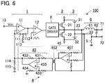
(2) As shown in FIG. 6, the inverting amplifiers 41 and 42 in the feedback circuit 4 of the embodiment described above may be replaced with an isolation type amplifier (isolation amplifier) 45. The isolation type amplifier 45 includes an inverting amplifier 451 and an isolation transformer 452. A primary coil of the isolation transformer 452 is connected between an output terminal of the inverting amplifier 451 and the reference node 33. Furthermore, a secondary coil of the isolation transformer 452 is connected between input terminals of the differential amplifier 43. A gain of the isolation type amplifier 45 (eventually, a total gain of the differential amplifier 43) may be set to a desired value according to a turn ratio between the primary coil and the secondary coil of the isolation transformer 452. In addition, as shown in FIG. 7, amplification in the differential amplifier 43 may be realized by the isolation type amplifier 45. That is, the differential amplifier 43 may be omitted. In the configuration in FIG. 7, the total gain of the differential amplifier 43 is set to a desired value according to the turn ratio of the isolation transformer 452 in the isolation type amplifier 45.
(3) As shown in FIG. 8, the inverting amplifiers 41 and 42 in the feedback circuit 4 of the embodiment may be replaced with one differential input amplifier 46. The differential input amplifier 46 inverts a polarity of a differential voltage between the output node 23 of the output stage 2 and the reference node 33 of the floating power supply 3 and amplifies the differential voltage. A voltage at an output terminal of the differential input amplifier 46 is output with reference to a reference voltage (the same ground line as the non-inverting input terminal) of the differential amplifier 43 (the inverting input terminal of the operational amplifier 435), and is supplied to an inverting input terminal of the differential amplifier 43.
(4) Although the voltage of a stage before the filter 6 (that is, the voltage between the output node 23 and the reference node 33) is fed back to the signal input unit 1 in the embodiment described above, a voltage of a stage (that is, the speaker terminals 71 and 72) after the filter 6 may be fed back to the signal input unit 1 by the feedback circuit 4, in addition to the above configuration.
For example, as shown in FIG. 9, a voltage of the speaker terminal 71 located at a stage after the filter 6 may be supplied to the inverting input terminal of the operational amplifier 413 in the inverting amplifier 41 via a low pass filter 471. Furthermore, a voltage of the speaker terminal 72 located at the stage after the filter 6 (that is, a voltage of the reference node 33) may be supplied to the inverting input terminal of the operational amplifier 423 in the inverting amplifier 42 via a low pass filter 472. Each of the low pass filters 471 and 472 includes, for example, a resistor and a capacitor, and passes components in an audio band (for example, band components at 20 kHz or less) included in the voltage of the stage after the filter 6. As will be understood from the above description, the feedback circuit 4 in FIG. 9 feeds the differential voltage between the output node 23 and the reference node 33 back to the signal input unit 1, similar to the embodiment described above. Furthermore, the feedback circuit 4 amplifies components in the audio band included in the voltage between the output node of the filter 6 and the reference node 33 and feeds the amplified differential voltage back to the signal input unit 1.
The above configuration has an advantage in that the voltage actually supplied to the speaker 7 is fed back to the signal input unit 1. As shown by a dotted line in FIG. 9, a capacitor 473 may be connected on a path from the output node 23 to the inverting input terminal of the operational amplifier 413. Furthermore, a capacitor 474 may be connected on a path from the reference node 33 to the inverting input terminal of the operational amplifier 423. The capacitor 473 and the resistor 411 function as a high pass filter to pass, for example, components exceeding an audio band of the voltage of the output node 23. Similarly, the capacitor 474 and the resistor 421 function as a high pass filter to pass, for example, components exceeding the audio band of the voltage of the reference node 33.
(5) In the power amplifier shown in FIG. 3, gains of the power amplification units 100 a and 100 b may be different. As shown in FIG. 3, even when the gains of the power amplification units 100 a and 100 b are different, in-phase components between voltage signals at the speaker terminals 71 b and 72 b of the power amplification unit 100 b (that is, in-phase components caused by the output voltage of the power amplification unit 100 a) are canceled out in the differential amplifier 43 b. Accordingly, the same effect as described above can be obtained.
(6) The embodiment describes, as an example of the power amplifier according to the present disclosure, a separately excited class-D amplifier that generates a PWM pulse train using a carrier signal generated by a periodic waveform generating circuit. However, the power amplifier according to the present disclosure may be a self-excited class-D amplifier that generates a PWM pulse train using self-excited oscillation that occurs in a closed loop including an output stage and a feedback circuit. Furthermore, the power amplifier according to the present disclosure may be a power amplifier other than a class-D amplifier.
(7) Although the floating power supply 3 is configured with the two DC power supplies 31 and 32 in the embodiment, a configuration of the floating power supply 3 is freely selected. For example, the floating power supply 3 may be configured with one DC power supply. Furthermore, although a neutral point of the floating power supply 3 is set as the reference node 33 in the embodiment, a node that is not a neutral point may be set as the reference node 33.
(8) A plurality of sets power amplifiers connected in series may be provided, and each of these sets may be connected in a Bridged Transless (BTL) manner.
For example, as shown in FIG. 10, an inverting circuit 82, an isolation type gate driver 8′, an output stage 2′, a reference potential switch 5′, and a filter 6′ may be added to the embodiment described above. The inverting circuit 82 inverts the output signal from the signal input unit 1 and inputs the resultant signal to the isolation type gate driver 8′. The isolation type gate driver 8′, the output stage 2′, and the filter 6′ operate similarly to the isolation type gate driver 8, the output stage 2, and the filter 6 in the embodiment described above. A speaker terminal 71 is installed on the output side of the filter 6 on the positive phase side, and a speaker terminal 72 is installed on the output side of the filter 6′ on the negative phase side. Although FIG. 10 shows the floating power supply 3′ separate from the floating power supply 3 for convenience, the floating power supply 3 is actually shared as the floating power supply 3′. In a case in which the floating power supply 3 is shared by the positive phase side and the negative phase side, the reference potential switch 5 is shared as the reference potential switch 5′.
The configuration shown in FIGS. 6 to 9 may be adopted for a BTL-connected power amplifier. For example, in the BTL-connected power amplifier as shown in FIG. 11, the inverting amplifiers 41 and 42 may be replaced with the isolation type amplifier 45 as in the example of FIG. 6 or 7. Furthermore, in the BTL-connected power amplifier as shown in FIG. 12, the inverting amplifiers 41 and 42 may be replaced by one differential input amplifier 46, as in the example of FIG. 8. In the BTL-connected power amplifier as shown in FIG. 13, a voltage at a stage after the filter 6 may be fed back to the signal input unit 1 by the feedback circuit 4.
(9) Although the embodiment shows the non-inverting type power amplifier 100, the present disclosure may be applied to an inverting type power amplifier. FIG. 14 is a circuit diagram showing a configuration of the inverting type power amplifier. As shown in FIG. 14, in the inverting type power amplifier, an input terminal 13 is connected to an inverting input terminal of an operational amplifier 11 in a signal input unit 1 via a capacitor 115 and a resistor 114. A non-inverting input terminal of the operational amplifier 11 is grounded. In the configuration shown in FIG. 14, for example, an inverting circuit (not shown) is provided at a stage before the power amplifier. A non-inverting type power amplifier including the inverting circuit and an inverting type power amplifier is configured as a whole.
(10) A plurality of sets of power amplifiers connected in series may be provided and connected in parallel.
(11) In the embodiments detailed above, examples of specific modifications of the present disclosure will now be described.
A power amplifier according to a preferred embodiment of the present disclosure includes: a signal input unit to which an input signal is applied; an output stage that is electrically isolated from the signal input unit, where the output stage is configured to amplify an output signal of the signal input unit based on a power supply voltage from a floating power supply; a reference potential switch that is inserted between a reference node of the power supply voltage generated by the floating power supply and a reference potential line; and a feedback circuit configured to amplify a differential voltage between the reference node and an object driven by an output of the output stage, and feed the amplified voltage back to the signal input unit.
It is possible to use multiple power amplifiers in combination, in addition to using one power amplifier alone. In the present disclosure, an example of a use aspect of a characteristic power amplifier includes an aspect in which output stages of power amplifiers are connected in series for use. For example, in a case in which two power amplifiers are used, a common input signal is applied to signal inputs of the two power amplifiers. In this case, a reference potential of one of the power amplifiers (hereinafter referred to as a first power amplifier) is turned to be in the ON state, and a reference potential switch of the other power amplifier (hereafter, a second power amplifier) is turned to be in the OFF state. An output stage of the first power amplifier, an output stage of the second power amplifier, and a load are connected in series.
In this configuration, the load is driven by a voltage obtained by adding an output voltage of the output stage of the first power amplifier to an output voltage of the output stage of the second power amplifier. Consequently, a current flows through the load. In this case, the output voltage of the second power amplifier is a voltage on which the output voltage of the first power amplifier is superimposed. However, in the first power amplifier, the output voltage is amplified with reference of the reference potential of the floating power supply by the feedback circuit and is fed back to the signal input units. The same is true of the second power amplifier. For example, potentials of the two nodes (one of the two nodes is the reference node) at which the output voltage of the second power amplifier is generated include the in-phase component caused by the output voltage of the first power amplifier. However, this in-phase component is canceled out in the feedback circuit and does not affect the feedback to the signal input unit. Therefore, it is possible to realize a series connection without changing a circuit configuration of the feedback circuit between the two power amplifiers. Although the series connection of two power amplifiers has been described by way of example, the same applies to a case in which three or more power amplifiers are connected in series.
In a preferred aspect of the present disclosure, the feedback circuit includes a first inverting amplifier configured to invert and amplify a voltage for the object driven by the output of the output stage, a second inverting amplifier configured to invert and amplify a voltage of the reference node of the floating power supply, and a differential amplifier configured to invert and amplify a difference between an output signal of the first inverting amplifier and an output signal of the second inverting amplifier.
The power amplifier according to a preferred embodiment of the present disclosure includes a filter configured to pass components in a specific band included in a differential voltage between an output node of the output stage and the reference node of the floating power supply, in which the feedback circuit amplifies components in an audio band included in the differential voltage between the output node and the reference node and the voltage between an output node of the filter and the reference node, and feeds the amplified differential voltage back to the signal input unit.
A power amplifier according to another aspect of the present disclosure includes two or more power amplification units, in which each of the two or more power amplification units includes: a signal input unit to which an input signal is applied; an output stage that is electrically isolated from the signal input unit, where the output stage is configured to amplify an output signal of the signal input unit based on a power supply voltage from a floating power supply; a reference potential switch that is inserted between a reference node of the power supply voltage generated by the floating power supply and a reference potential line; and a feedback circuit configured to amplify a differential voltage between the reference node and an object driven by an output of the output stage, and feed the amplified differential voltage back to the signal input unit.
DESCRIPTION OF REFERENCE SIGNS
  • 100: Power amplifier
  • 100 a, 100 b, 100 c: Power amplification unit
  • 1, 1 a, 1 b, 1 c: Signal input unit
  • 8, 8 a, 8 b, 8 c: Insulation type gate driver
  • 3, 3 a, 3 b, 3 c: Floating power supply
  • 6, 6 a, 6 b, 6 c: Filter
  • 71, 71 a, 71 b, 71 c, 72, 72 a, 72 b, 72 c: Speaker terminal
  • 7: Speaker
  • 4, 4 a, 4 b, 4 c: Feedback circuit
  • 41, 41 a, 41 b, 41 c, 42, 42 a, 42 b, 42 c: Inverting amplifier
  • 43, 43 a, 43 b, 43 c: Differential amplifier
  • 5, 5 a, 5 b, 5 c: Reference potential switch

Claims (4)

What is claimed is:
1. A power amplifier comprising:
a signal input unit to which an input signal is applied;
an output stage that is electrically isolated from the signal input unit, where the output stage is configured to amplify an output signal of the signal input unit based on a power supply voltage from a floating power supply;
a reference potential switch that is inserted between a reference node of the power supply voltage generated by the floating power supply and a reference potential line; and
a feedback circuit configured to amplify a differential voltage between the reference node and an object driven by an output of the output stage, and feed the amplified differential voltage back to the signal input unit.
2. The power amplifier according to claim 1, wherein the feedback circuit includes:
a first inverting amplifier configured to invert and amplify a voltage for the object driven by the output of the output stage;
a second inverting amplifier configured to invert and amplify a voltage of the reference node of the floating power supply; and
a differential amplifier configured to invert and amplify a difference between an output signal of the first inverting amplifier and an output signal of the second inverting amplifier.
3. The power amplifier according to claim 1, further comprising a filter configured to pass components in a specific band included in a differential voltage between an output node of the output stage and the reference node of the floating power supply, and
wherein the feedback circuit is configured to amplify components in an audio band included in the differential voltage between the output node and the reference node and a differential voltage between an output node of the filter and the reference node, and feeds the amplified differential voltage back to the signal input unit.
4. A power amplifier comprising: two or more power amplification units, wherein each of the two or more power amplification units includes:
a signal input unit to which an input signal is applied;
an output stage that is electrically isolated from the signal input unit, where the output stage is configured to amplify an output signal of the signal input unit based on a power supply voltage from a floating power supply;
a reference potential switch that is inserted between a reference node of the power supply voltage generated by the floating power supply and a reference potential line; and
a feedback circuit configured to amplify a differential voltage between the reference node and an object driven by an output of the output stage, and feed the amplified differential voltage back to the signal input unit.
US16/383,818 2016-10-21 2019-04-15 Power amplifier Active 2037-11-23 US10819293B2 (en)

Applications Claiming Priority (3)

Application Number Priority Date Filing Date Title
JP2016207035 2016-10-21
JP2016-207035 2016-10-21
PCT/JP2017/036987 WO2018074317A1 (en) 2016-10-21 2017-10-12 Power amplifier

Related Parent Applications (1)

Application Number Title Priority Date Filing Date
PCT/JP2017/036987 Continuation WO2018074317A1 (en) 2016-10-21 2017-10-12 Power amplifier

Publications (2)

Publication Number Publication Date
US20190245494A1 US20190245494A1 (en) 2019-08-08
US10819293B2 true US10819293B2 (en) 2020-10-27

Family

ID=62019272

Family Applications (1)

Application Number Title Priority Date Filing Date
US16/383,818 Active 2037-11-23 US10819293B2 (en) 2016-10-21 2019-04-15 Power amplifier

Country Status (3)

Country Link
US (1) US10819293B2 (en)
JP (1) JP6819690B2 (en)
WO (1) WO2018074317A1 (en)

Families Citing this family (3)

* Cited by examiner, † Cited by third party
Publication number Priority date Publication date Assignee Title
CN113054928B (en) * 2021-03-12 2023-08-29 苏州至盛半导体科技有限公司 D-type power amplifier dynamic boosting closed-loop controller and D-type power amplifier with dynamic boosting function
JP7647201B2 (en) 2021-03-17 2025-03-18 ヤマハ株式会社 Class D Amplifier
NO347259B1 (en) * 2022-06-15 2023-08-14 Zenitel Norway As An improved audio amplifier with a transformer-less output stage and a method for operating an improved audio amplifier

Citations (8)

* Cited by examiner, † Cited by third party
Publication number Priority date Publication date Assignee Title
JPS5587016U (en) 1978-12-11 1980-06-16
JPS63111710A (en) 1986-10-29 1988-05-17 Toshiba Corp Drive circuit for pulse amplifier
US20070236825A1 (en) * 2006-04-10 2007-10-11 Texas Instruments Incorporated Differential Voice Coil Motor Control
JP2009100352A (en) 2007-10-18 2009-05-07 Seiko Npc Corp Digital amplifier circuit
US7986187B1 (en) 2010-03-04 2011-07-26 Bose Corporation Versatile audio power amplifier
US20130088294A1 (en) 2011-10-06 2013-04-11 Douglas E. Heineman Attenuating Non-Linear Noise in An Amplifier with Alternating DC -offset Correction
US8890608B2 (en) * 2012-02-29 2014-11-18 Texas Instruments Incorporated Digital input class-D audio amplifier
US10554189B2 (en) * 2017-06-02 2020-02-04 Cirrus Logic, Inc. Analogue signal paths

Patent Citations (11)

* Cited by examiner, † Cited by third party
Publication number Priority date Publication date Assignee Title
JPS5587016U (en) 1978-12-11 1980-06-16
JPS63111710A (en) 1986-10-29 1988-05-17 Toshiba Corp Drive circuit for pulse amplifier
US20070236825A1 (en) * 2006-04-10 2007-10-11 Texas Instruments Incorporated Differential Voice Coil Motor Control
US7522368B2 (en) * 2006-04-10 2009-04-21 Texas Instruments Incorporated Differential voice coil motor control
JP2009100352A (en) 2007-10-18 2009-05-07 Seiko Npc Corp Digital amplifier circuit
US7986187B1 (en) 2010-03-04 2011-07-26 Bose Corporation Versatile audio power amplifier
WO2011109152A1 (en) 2010-03-04 2011-09-09 Bose Corporation Versatile audio power amplifier
JP2013521699A (en) 2010-03-04 2013-06-10 ボーズ・コーポレーション General purpose audio power amplifier
US20130088294A1 (en) 2011-10-06 2013-04-11 Douglas E. Heineman Attenuating Non-Linear Noise in An Amplifier with Alternating DC -offset Correction
US8890608B2 (en) * 2012-02-29 2014-11-18 Texas Instruments Incorporated Digital input class-D audio amplifier
US10554189B2 (en) * 2017-06-02 2020-02-04 Cirrus Logic, Inc. Analogue signal paths

Non-Patent Citations (2)

* Cited by examiner, † Cited by third party
Title
International Search Report issued in Intl. Appln. No. PCT/JP2017/036987 dated Jan. 9, 2018. English translation provided.
Written Opinion issued in Intl. Appln. No. PCT/JP2017/036987 dated Jan. 9, 2018.

Also Published As

Publication number Publication date
WO2018074317A1 (en) 2018-04-26
JP6819690B2 (en) 2021-01-27
US20190245494A1 (en) 2019-08-08
JPWO2018074317A1 (en) 2019-08-22

Similar Documents

Publication Publication Date Title
US6707337B2 (en) Self-operating PWM amplifier
KR100604967B1 (en) Power amplifier circuit
US7944297B2 (en) Class D amplifier
US9344045B2 (en) Amplifier and method of amplifying a differential signal
US10819293B2 (en) Power amplifier
US6476674B2 (en) Method and apparatus for error correction of amplifier
US7911273B2 (en) Reduction of power consumption and EMI of a switching amplifier
US9602070B2 (en) Power amplifying device
US11171617B2 (en) Power amplifying device and audio equipment
US20110116653A1 (en) plop-free amplifier
EP1977504B1 (en) Single-ended amplifier
EP3223427A1 (en) Btl output self-oscillating class d amplifier
US10164581B2 (en) Self-oscillating amplifier with high order loop filter
US7292098B2 (en) Operational amplifier
TW201924213A (en) An error amplifier
US7633339B2 (en) Differential amplifier
EP4199352A1 (en) Voltage and current sense circuits for measuring a load connected to a power amplifier
US7439801B2 (en) Amplifier circuit with multiple power supplies
US11245368B2 (en) Class D amplifier
KR100770747B1 (en) Digital Amplifier and Voice Playback Method
JP2007209038A (en) Power amplifier circuit
JP2014072613A (en) Class d amplification circuit
JPH0335846B2 (en)
JP4461480B2 (en) amplifier

Legal Events

Date Code Title Description
AS Assignment

Owner name: YAMAHA CORPORATION, JAPAN

Free format text: ASSIGNMENT OF ASSIGNORS INTEREST;ASSIGNOR:OHTANI, YOHEI;REEL/FRAME:048881/0100

Effective date: 20190411

FEPP Fee payment procedure

Free format text: ENTITY STATUS SET TO UNDISCOUNTED (ORIGINAL EVENT CODE: BIG.); ENTITY STATUS OF PATENT OWNER: LARGE ENTITY

STPP Information on status: patent application and granting procedure in general

Free format text: NOTICE OF ALLOWANCE MAILED -- APPLICATION RECEIVED IN OFFICE OF PUBLICATIONS

STCF Information on status: patent grant

Free format text: PATENTED CASE

MAFP Maintenance fee payment

Free format text: PAYMENT OF MAINTENANCE FEE, 4TH YEAR, LARGE ENTITY (ORIGINAL EVENT CODE: M1551); ENTITY STATUS OF PATENT OWNER: LARGE ENTITY

Year of fee payment: 4