US10819071B2 - Connector structure that is reconfigurable to accommodate either an STP cable or a UTP cable - Google Patents
Connector structure that is reconfigurable to accommodate either an STP cable or a UTP cable Download PDFInfo
- Publication number
- US10819071B2 US10819071B2 US16/340,733 US201716340733A US10819071B2 US 10819071 B2 US10819071 B2 US 10819071B2 US 201716340733 A US201716340733 A US 201716340733A US 10819071 B2 US10819071 B2 US 10819071B2
- Authority
- US
- United States
- Prior art keywords
- utp
- stp
- dielectric
- width direction
- connection terminal
- Prior art date
- Legal status (The legal status is an assumption and is not a legal conclusion. Google has not performed a legal analysis and makes no representation as to the accuracy of the status listed.)
- Active
Links
- 238000003780 insertion Methods 0.000 claims description 19
- 230000037431 insertion Effects 0.000 claims description 19
- 239000004020 conductor Substances 0.000 description 53
- 230000013011 mating Effects 0.000 description 35
- 238000005192 partition Methods 0.000 description 13
- 229920003002 synthetic resin Polymers 0.000 description 6
- 239000000057 synthetic resin Substances 0.000 description 6
- 238000002788 crimping Methods 0.000 description 4
- 239000002184 metal Substances 0.000 description 3
- 239000000463 material Substances 0.000 description 2
- 230000000717 retained effect Effects 0.000 description 2
- 238000000926 separation method Methods 0.000 description 2
- 238000005452 bending Methods 0.000 description 1
- 238000004519 manufacturing process Methods 0.000 description 1
- 230000002093 peripheral effect Effects 0.000 description 1
- 230000005855 radiation Effects 0.000 description 1
- 238000005476 soldering Methods 0.000 description 1
Images


Classifications
-
- H—ELECTRICITY
- H01—ELECTRIC ELEMENTS
- H01R—ELECTRICALLY-CONDUCTIVE CONNECTIONS; STRUCTURAL ASSOCIATIONS OF A PLURALITY OF MUTUALLY-INSULATED ELECTRICAL CONNECTING ELEMENTS; COUPLING DEVICES; CURRENT COLLECTORS
- H01R13/00—Details of coupling devices of the kinds covered by groups H01R12/70 or H01R24/00 - H01R33/00
- H01R13/646—Details of coupling devices of the kinds covered by groups H01R12/70 or H01R24/00 - H01R33/00 specially adapted for high-frequency, e.g. structures providing an impedance match or phase match
- H01R13/6461—Means for preventing cross-talk
- H01R13/6463—Means for preventing cross-talk using twisted pairs of wires
-
- H—ELECTRICITY
- H01—ELECTRIC ELEMENTS
- H01R—ELECTRICALLY-CONDUCTIVE CONNECTIONS; STRUCTURAL ASSOCIATIONS OF A PLURALITY OF MUTUALLY-INSULATED ELECTRICAL CONNECTING ELEMENTS; COUPLING DEVICES; CURRENT COLLECTORS
- H01R13/00—Details of coupling devices of the kinds covered by groups H01R12/70 or H01R24/00 - H01R33/00
- H01R13/646—Details of coupling devices of the kinds covered by groups H01R12/70 or H01R24/00 - H01R33/00 specially adapted for high-frequency, e.g. structures providing an impedance match or phase match
- H01R13/6473—Impedance matching
- H01R13/6474—Impedance matching by variation of conductive properties, e.g. by dimension variations
-
- H—ELECTRICITY
- H01—ELECTRIC ELEMENTS
- H01R—ELECTRICALLY-CONDUCTIVE CONNECTIONS; STRUCTURAL ASSOCIATIONS OF A PLURALITY OF MUTUALLY-INSULATED ELECTRICAL CONNECTING ELEMENTS; COUPLING DEVICES; CURRENT COLLECTORS
- H01R24/00—Two-part coupling devices, or either of their cooperating parts, characterised by their overall structure
- H01R24/20—Coupling parts carrying sockets, clips or analogous contacts and secured only to wire or cable
- H01R24/22—Coupling parts carrying sockets, clips or analogous contacts and secured only to wire or cable with additional earth or shield contacts
-
- H—ELECTRICITY
- H01—ELECTRIC ELEMENTS
- H01R—ELECTRICALLY-CONDUCTIVE CONNECTIONS; STRUCTURAL ASSOCIATIONS OF A PLURALITY OF MUTUALLY-INSULATED ELECTRICAL CONNECTING ELEMENTS; COUPLING DEVICES; CURRENT COLLECTORS
- H01R24/00—Two-part coupling devices, or either of their cooperating parts, characterised by their overall structure
- H01R24/60—Contacts spaced along planar side wall transverse to longitudinal axis of engagement
Definitions
- the present invention relates to a connector structure.
- a twisted pair cable in which electric wires are twisted together is less susceptible to noise than a simple parallel line and has less noise radiation, so that the twisted pair cable is suitably used for an in-vehicle network or the like.
- an STP (shielded twisted pair) cable and a UTP (unshielded twisted pair) cable are known.
- the electric wires are surrounded by a shield conductor, so that the STP cable has stronger resistance to noise.
- Japanese Patent No. 5333632 discloses a connector including an inner conductor terminal connected to an end portion of an STP cable, an inner housing (dielectric) accommodating the inner conductor terminal, a shield shell connected to a shield conductor of the STP cable and surrounding the inner housing, and an outer housing accommodating the shield shell.
- Japanese Patent No. 5087487 discloses a connector including a connection terminal connected to an end portion of a UTP cable and a connector body (dielectric) having a terminal accommodating portion which accommodates the connection terminal.
- the connectors of Japanese Patent No. 5333632 and Japanese Patent No. 50874872 include a common configuration that each electric wire of the UTP cable and the STP cable is connected to a terminal and the terminal is accommodated in the dielectric.
- the STP cable can be replaced with the UTP cable or if the UTP cable can be replaced with the STP cable while making use of a common structural portion in the connectors, mold design becomes easy, and the cost can be reduced.
- mold design becomes easy, and the cost can be reduced.
- the present invention has been completed based on the above circumstances, and its purpose is to provide a connector structure capable of replacing an STP cable and a UTP cable without making a large structural change.
- a connector structure of the present invention includes a UTP connection terminal which is connected to each electric wire of a UTP cable and has a box portion to which a male terminal is inserted and connected, an STP connection terminal which is connected to each electric wire of an STP cable and has a box portion to which a male terminal is inserted and connected, a UTP dielectric which has an accommodating portion in which the UTP connection terminal is accommodated, and an STP dielectric which has an accommodating portion in which the STP connection terminal is accommodated.
- a receiving portion and an elastic contact piece facing the receiving portion are arranged in each of the box portions of the UTP connection terminal and the STP connection terminal, the elastic contact piece protrudes inside the box portion with a protruding amount larger than that of the receiving portion, and the male terminal is held between the receiving portion and the elastic contact piece.
- the accommodating portions are arranged in pairs in a width direction perpendicular to an insertion direction of the male terminal, and a widthwise clearance of the pair of accommodating portions is shorter in the UTP dielectric than in the STP dielectric.
- the UTP connection terminals are accommodated in the pair of accommodating portions of the UTP dielectric such that the elastic contact pieces thereof are located inside so as to be close to each other in the width direction and the receiving portions thereof are located outside so as to be spaced apart from each other in the width direction, and the STP connection terminals are accommodated in the pair of accommodating portions of the STP dielectric such that the elastic contacts piece thereof are located outside so as to be spaced apart from each other in the width direction and the receiving portions thereof are located inside so as to be close to each other in the width direction.
- the accommodating portions in pairs of the UTP dielectric are closer to each other in the width direction than those of the STP dielectric, when the UTP connection terminals connected to respective electric wires of the UTP cable are accommodated in the pair of accommodating portions of the UTP dielectric, the impedance can be reduced.
- the accommodating portions in pairs of the STP dielectric are spaced more apart from each other in the width direction than those of the UTP dielectric, when the STP connection terminals connected to respective electric wires of the STP cable are accommodated in the pair of accommodating portions of the STP dielectric, the impedance can be increased. As a result, it is possible to suitably adjust the impedance between the UTP cable side and the STP cable side.
- a widthwise clearance (pitch width) between the male terminals to be connected to the UTP connection terminals and a widthwise clearance (pitch width) between the male terminals to be connected to the STP connection terminals can be identical to the same pitch width. Accordingly, it is not necessary to make a large structural change as a whole, and thus it is possible to easily replace the UTP cable and the STP cable.
- the box portion of the UTP connection terminal has the same shape as the box portion of the STP connection terminal. According to this constitution, the box portion of each terminal can be manufactured with the same mold, with the result that the manufacturing cost can be reduced.
- FIG. 1 is an exploded perspective view of an UTP connector of Embodiment 1 of the present invention.
- FIG. 2 is an exploded perspective view showing UTP connection terminals and a lower dielectric.
- FIG. 3 is a perspective view showing a state in which the UTP connection terminals are accommodated in accommodating portions of the lower dielectric.
- FIG. 4 is an exploded perspective view showing the lower dielectric in which the UTP connection terminals are accommodated and an upper dielectric.
- FIG. 5 is a perspective view of a UTP dielectric in which the lower dielectric and the upper dielectric are held in a combined state.
- FIG. 6 is an exploded perspective view showing the UTP dielectric and a UTP housing.
- FIG. 7 is a perspective view of the UTP connector.
- FIG. 8 is a cross-sectional view of the UTP connector in a side view direction.
- FIG. 9 is a cross-sectional view of the UTP connector in a plan view direction.
- FIG. 10 is a planar cross-sectional view showing the UTP connector and a mating UTP connector in a fitted state.
- FIG. 11 is a front cross-sectional view showing the UTP connection terminals and male terminals in a connected state.
- FIG. 12 is a front view of the mating UTP connector.
- FIG. 13 is an exploded perspective view of an STP connector.
- FIG. 14 is an exploded perspective view showing STP connection terminals and a lower dielectric.
- FIG. 15 is an exploded perspective view showing the lower dielectric in which the STP connection terminals are accommodated and an upper dielectric.
- FIG. 16 is a perspective view of a STP dielectric in which the lower dielectric and the upper dielectric are held in a combined state.
- FIG. 17 is an exploded perspective view showing the STP dielectric and a lower outer conductor.
- FIG. 18 is a perspective view showing a state in which the STP dielectric is supported by the lower outer conductor.
- FIG. 19 is an exploded perspective view showing the lower outer conductor supporting the STP dielectric and an upper outer conductor.
- FIG. 20 is a perspective view of an outer conductor in which the lower outer conductor and the upper outer conductor are held in a combined state and which is connected to a shield conductor of an STP cable.
- FIG. 21 is an exploded perspective view showing the outer conductor enclosing the STP dielectric, and an STP housing.
- FIG. 22 is a perspective view of the STP connector.
- FIG. 23 is a cross-sectional view of the STP connector in a side view direction.
- FIG. 24 is a cross-sectional view of the STP connector in a plan view direction.
- FIG. 25 is a planar cross-sectional view showing the STP connector and a mating STP connector in a fitted state.
- FIG. 26 is a front cross-sectional view showing the STP connection terminals and male terminals in a connected state.
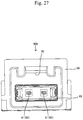
- FIG. 27 is a front view of the mating STP connector.
- a connector structure of this embodiment is used for an in-vehicle communication network system and includes a UTP connector 20 A provided at an end portion of a UTP cable 10 A and an STP connector 20 B provided at an end portion of an STP cable 10 B, and one of the connectors 20 A and 20 B can be selectively used.
- the UTP connector 20 A and the STP connector 20 B have a structural portion in common or approximate to each other, and it is possible to replace the UTP cable 10 A and the STP cable 10 B while adjusting impedance.
- the UTP connector 20 A is fitted to a mating UTP connector 90 A and, as shown in FIG. 1 , includes a UTP connection terminal 21 A, a UTP dielectric 22 A, and a UTP housing 23 A.
- the STP connector 20 B is fitted to a mating STP connector 90 B and, as shown in FIG. 13 , includes an STP connection terminal 21 B, an STP dielectric 22 B, an outer conductor 24 B, and an STP housing 23 B.
- the UTP cable 10 A is constituted of a pair of twisted electric wires 11 and a sheath 12 surrounding the electric wires 11 .
- the electric wire 11 is constituted of a conductor portion and a covering portion surrounding the conductor portion. The respective end portions of the electric wires 11 are exposed from the sheath 12 and connected to the UTP connection terminals 21 A respectively.
- the UTP connection terminals 21 A connected to the electric wires 11 of the UTP cable 10 A are constructed in the same shape.
- each UTP connection terminal 21 A is electrically connected to a male terminal 91 provided in a mating UTP connector 90 A.
- the UTP connection terminal 21 A is integrally formed by, for example, bending a conductive metal plate material and has an elongated shape as a whole in the front-rear direction (horizontal direction in FIG. 9 ).
- the UTP connection terminal 21 A has a band plate-shaped base plate portion 25 extending in the front-rear direction.
- a box portion 27 having a substantially rectangular tubular shape is provided at a front end portion of the base plate portion 25
- an open barrel-shaped barrel portion 28 is provided at a rear end portion of the base plate portion 25 .
- the barrel portion 28 is electrically and mechanically connected to the conductor portion and the covering portion of the electric wire 11 , respectively.
- a swaging ring 29 separate from the UTP connection terminal 21 A is crimped and connected to an end portion of the sheath 12 of the UTP cable 10 A.
- a receiving portion 31 and an elastic contact piece 32 protrude so as to face each other in the width direction.
- the receiving portion 31 having a trapezoidal cross section is fixedly provided on the base plate portion 25 side, and the band plate-shaped elastic contact piece 32 is protrudingly provided on a top plate portion 33 side opposite to the base plate portion 25 .
- the elastic contact piece 32 is formed to extend forward from the rear end side of the top plate portion 33 in a cantilever fashion, and is flexibly deformable with the rear end side of the top plate portion 33 as a fulcrum.
- the amount of protrusion into the box portion 27 (dimension in the vertical direction in FIG. 9 ) is larger in the elastic contact piece 32 than in the receiving portion 31 .
- a top portion of the elastic contact piece 32 is located closer to the center of the box portion 27 than an end surface of the receiving portion 31 .
- the UTP dielectric 22 A is made of a synthetic resin and is constituted of an upper dielectric 35 and a lower dielectric 36 that can be split vertically.
- the upper dielectric 35 has a substantially rectangular plate shape in a plan view and has a locking protrusion 37 , which can be locked to the UTP housing 23 A, at the widthwise center of the upper surface.
- the lower surface of the upper dielectric 35 is provided with a recess 38 (see FIG. 8 ) which positions upper portions of the UTP connection terminals 21 A in a parallel state and positions an upper portion of the swaging ring 29 .
- Both widthwise end portions of the upper dielectric 35 are provided with a pair of front and rear attachment pieces 39 protruding downward.
- the lower dielectric 36 has a substantially rectangular plate shape in a plan view, has a pair of front and rear attachment receiving portions 41 each having a rectangular recessed shape at both widthwise end portions, and has attachment protrusions 42 each provided on an inner surface of each attachment receiving portion 41 .
- Each attachment piece 39 is fitted to each attachment receiving portion 41 , and a distal end portion of the attachment piece 39 is hooked and locked to the attachment protrusion 42 , whereby the lower dielectric 36 and the upper dielectric 35 are held in a combined state while the UTP connection terminals 21 A are sandwiched therebetween.
- the upper surface of the lower dielectric 36 has accommodating portions 26 which accommodate lower portions of the UTP connection terminals 21 A in a parallel state.
- the accommodating portions 26 each have a cross-sectional shape corresponding to the outer shape of the UTP connection terminal 21 A, and are provided in pairs on both sides in the width direction width direction with the partition wall 43 sandwiched therebetween.
- tab insertion holes 69 through which the tab portions 92 can be inserted in communication with the accommodating portions 26 are provided as openings on a front surface of the UTP dielectric 22 A.
- One of the accommodating portions 26 (the upper side in FIG. 2 ) has a plate piece-like protruding piece portion 45 protruding upward from a side edge of the partition wall 43
- the other accommodating portion 26 (the lower side in FIG. 2 ) has a recess 44 formed by recessing the partition wall 43 in a cross-sectionally rectangular shape.
- the partition wall 43 has a step portion 52 having a stepped shape at a position adjacent to the protruding piece portion 45 and the recess 44 .
- each UTP connection terminal 21 A is disposed such that the base plate portion 25 is disposed along a widthwise outer side surface of the accommodating portion 26 (an inner surface of an outer side wall facing the partition wall 43 ) and a rear end of the box portion 27 on the top plate portion 33 side is disposed along the step portion 52 , so that the UTP connection terminals 21 A are disposed in a belly-to-belly fashion.
- the protruding portion 34 of the UTP connection terminal 21 A accommodated in one of the accommodating portions 26 is placed and supported on the protruding piece portion 45 , and the protruding portion 34 of the UTP connection terminal 21 A accommodated in the other accommodating portion 26 is inserted into the recess 44 .
- a recessed portion 46 which positions and holds a lower portion of the swaging ring 29 is provided so as to be contiguous with a rear portion of the accommodating portions 26 .
- the UTP housing 23 A is made of a synthetic resin and, as shown in FIG. 6 , has a substantially rectangular tubular housing body 47 .
- a lock arm 48 is protrudingly provided in the central portion in the width direction.
- the lock arm 48 is formed to extend rearward from an upper front end portion of the housing body 47 in a cantilever fashion, and configured to elastically lock a lock receiving portion 93 of the mating UTP connector 90 A and thereby hold the UTP connector 20 A and the mating UTP connector 90 A in a fitted state.
- an insertion portion 49 is provided so as to be opened in the front-rear direction. As shown in FIG.
- the UTP dielectric 22 A can be fitted into the insertion portion 49 .
- the upper surface of the inner wall of the insertion portion 49 is provided with a lance 51 protruding forward in a cantilever fashion.
- the UTP dielectric 22 A is inserted into the insertion portion 49 from behind, the lance 51 is then flexibly deformed by the locking protrusion 37 , and thereafter the lance 51 returns and elastically locks the locking protrusion 37 , whereby the UTP dielectric 22 A is held in the UTP housing 23 A.
- the mating UTP connector 90 A has a hood portion 94 made of a synthetic resin.
- the UTP housing 23 A can be fitted into the hood portion 94 , and the hood portion 94 is supported on a printed circuit board (not shown).
- the lock receiving portion 93 to be locked to the lock arm 48 is protrudingly provided.
- pegs 95 each formed of a metal plate material are attached to outer surfaces of both side walls of the hood portion 94 .
- the peg 95 are soldered to a surface of the circuit board, whereby the mating UTP connector 90 A is fixed to the circuit board via the pegs 95 .
- a pair of the male terminals 91 is attached to the hood portion 94 in the width direction.
- Each of the male terminals 91 has a square linear shape (square pin shape) as a whole and is bent at a substantially right angle in the middle of the length direction.
- Each of the male terminals 91 has the tab portion 92 protruding into the hood portion 94 .
- the tab portions 92 of the male terminals 91 are arranged in parallel with a pitch width corresponding to a widthwise clearance (hereinafter referred to as a pitch width) between the insertion regions 53 of the UTP connection terminals 21 A accommodated in the accommodating portions 26 .
- Each male terminal 91 has a portion protruding to the outside of the hood portion 94 , and this portion is mounted and connected on the surface of the circuit board (not shown) by soldering.
- the STP cable 10 B includes the pair of twisted electric wires 11 , a shield conductor 13 such as a braided wire which surrounds and shields the electric wires 11 , and the sheath 12 which surrounds the shield conductor 13 .
- An end portion of each of the electric wires 11 and an end portion of the shield conductor 13 are exposed from the sheath 12 , and the end portion of the shield conductor 13 is folded back and attached to the outer circumference side of the sheath 12 .
- the respective end portions of the electric wires 11 are connected to the STP connection terminals 21 B respectively.
- the STP connection terminals 21 B connected to the electric wires 11 of the STP cable 10 B are constructed in the same shape.
- each STP connection terminal 21 B is connected to a male terminal 91 provided in a mating STP connector 90 B.
- the STP connection terminal 21 B has substantially the same shape as the UTP connection terminal 21 A, and has the box portion 27 and the barrel portion 28 , and includes the receiving portion 31 , the elastic contact piece 32 and the protruding portion 34 in the box portion 27 .
- the STP dielectric 22 B is made of a synthetic resin and is constituted of an upper dielectric 35 and a lower dielectric 36 that can be split vertically.
- the upper dielectric 35 has a substantially rectangular plate shape in a plan view and has positioning protruding portions 54 on the upper surface and both side surfaces thereof for the outer conductor 24 B. Both widthwise end portions of the upper dielectric 35 are provided with attachment pieces 39 similarly to the upper dielectric 35 of the UTP dielectric 22 A.
- the lower dielectric 36 is provided with the attachment receiving portions 41 and the attachment protrusions 42 , and by engagement between the attachment pieces 39 and the attachment protrusions 42 , the lower dielectric 36 and the upper dielectric 35 are held in a combined state while the STP connection terminals 21 B are sandwiched therebetween.
- the STP connector 20 B is not provided with the swaging ring 29 , and a rear portion of each of the upper dielectric 35 and the lower dielectric 36 does not have a portion which receives the swaging ring 29 (corresponding to the recess 38 and the recessed portion 46 ). Accordingly, the front-rear dimensions of the upper dielectric 35 and the lower dielectric 36 of the STP dielectric 22 B are shorter than those of the UTP dielectric 22 A.
- the upper surface of the lower dielectric 36 is provided with the accommodating portions 26 which position and hold the lower portions of the STP connection terminals 21 B in a parallel state.
- the accommodating portions 26 each have a cross-sectional shape corresponding to the outer shape of the STP connection terminal 21 B, and are provided in pairs on both sides in the width direction with the partition wall 43 sandwiched therebetween so as to correspond to the STP connection terminals 21 B.
- tab insertion holes 69 through which the tab portions 92 can be inserted in communication with the accommodating portion 26 are provided as openings on a front surface of the STP dielectric 22 B.
- the thickness (dimension in the width direction) of the partition wall 43 of the STP dielectric 22 B is slightly larger than the thickness of the partition wall 43 of the UTP dielectric 22 A. Accordingly, the pitch width between the accommodating portions 26 of the STP dielectric 22 B is larger than the pitch width between the accommodating portions 26 of the UTP dielectric 22 A.
- One of the accommodating portions 26 (upper side in FIG. 14 ) has a recess 44 formed by recessing the inner surface of the outer side wall facing the partition wall 43 in a cross-sectionally rectangular shape, and the other accommodating portion 26 (lower side in FIG. 14 ) has a plate piece-like protruding piece portion 45 protruding upward from a side edge of the outer side wall.
- the partition wall 43 has the step portion 52 having a stepped shape at a position adjacent to the recess 44 and the protruding piece portion 45 .
- each STP connection terminal 21 B is disposed such that the base plate portion 25 is disposed along an inner surface of the partition wall 43 and a rear end of the box portion 27 on the top plate portion 33 side is disposed along the step portion 52 , so that the STP connection terminals 21 B are disposed in a back-to-back fashion.
- the protruding portion 34 of the STP connection terminal 21 B accommodated in one of the accommodating portions 26 is inserted into the recess 44 , and the protruding portion 34 of the STP connection terminal 21 B accommodated in the other accommodating portion 26 is placed and supported on the protruding piece portion 45 .
- the outer conductor 24 B is made of a conductive metal and is constituted of an upper outer conductor 56 and a lower outer conductor 57 that can be split vertically.
- the upper outer conductor 56 has an upper shell portion 58 having a substantially rectangular shape in a plan view and an open barrel-shaped upper barrel portion 59 continuing to a rear portion of the upper shell portion 58 .
- the upper shell portion 58 is disposed so as to cover the upper dielectric 35 from above.
- a flat plate portion of the upper shell portion 58 has the locking protrusion 37 at a widthwise central portion of the upper surface and has an upper positioning hole 61 in front of the locking protrusion 37 .
- the upper shell portion 58 has side plate portions hanging from both widthwise ends of the flat plate portion and has a pair of front and rear holding protrusions 62 on inner surfaces of the side plate portions as shown in FIG. 24 .
- the upper barrel portion 59 has protruding piece portions which protrude downward from both widthwise side edges thereof while being displaced from each other in the front-rear direction.
- the lower outer conductor 57 has a lower shell portion 63 having a substantially rectangular shape in a plan view and an open barrel-shaped lower barrel portion 64 continuing to a rear portion of the lower shell portion 63 .
- the lower shell portion 63 is disposed so as to cover the lower dielectric 36 from below.
- the lower shell portion 63 has side plate portions standing from both widthwise ends of a flat plate portion and has a pair of front and rear holding holes 65 in the side plate portions.
- the central portion in the front-rear direction of each side plate portion of the lower shell portion 63 is provided with a lower positioning hole 66 opened to the upper end.
- the lower barrel portion 64 has protruding piece portions which protrude upward from both widthwise end edges while being displaced from each other in the front-rear direction.
- the side plate portions of the upper shell portion 58 cover the side plate portions of the lower shell portion 63 from the outside, and the holding protrusions 62 are inserted and locked in the holding holes 65 (see FIG. 24 ).
- the STP housing 23 B is made of a synthetic resin and, as shown in FIG. 21 , has a substantially rectangular tubular housing body 47 .
- the STP housing 23 B has substantially the same shape as the UTP housing 23 A, and has the lock arm 48 , the insertion portion 49 , and the lance 51 .
- the engagement partner of the lance 51 is the locking protrusion 37 of the upper outer conductor 56 .
- the mating STP connector 90 B has a hood portion 94 made of a synthetic resin.
- the mating STP connector 90 B has a configuration similar to that of the mating UTP connector 90 A and has the hood portion 94 , the lock receiving portion 93 , the pegs 95 , and the pair of male terminals 91 .
- the pitch width between the male terminals 91 of the mating STP connector 90 B is the same as the pitch width between the male terminals 91 of the mating UTP connector 90 A.
- each UTP connection terminal 21 A Upon assembling the UTP connector 20 A, the barrel portion 28 of each UTP connection terminal 21 A is first connected to the end portion of each electric wire 11 of the UTP cable 10 A by crimping. Subsequently, each of the UTP connection terminals 21 A is positioned and inserted into the accommodating portion 26 of the lower dielectric 36 from above, and, at the same time, the swaging ring 29 fitted to the UTP cable 10 A is positioned and inserted into the recessed portion 46 of the lower dielectric 36 (see FIGS. 2 and 3 ).
- the UTP connection terminal 21 A accommodated in one of the accommodating portions 26 is inserted with the protruding portion 34 facing upward, and the UTP connection terminal 21 A accommodated in the other accommodating portion 26 is inserted with the protruding portion 34 facing downward.
- the upper dielectric 35 is then covered on the lower dielectric 36 from above, and the attachment pieces 39 elastically lock the attachment protrusions 42 , whereby the upper dielectric 35 and the lower dielectric 36 are held in a combined state (see FIGS. 4 and 5 ).
- the UTP dielectric 22 A is inserted into the insertion portion 49 of the UTP housing 23 A from behind (see FIGS. 6 and 7 ).
- the lance 51 elastically locks the locking protrusion 37 of the UTP dielectric 22 A, so that the UTP dielectric 22 A is held in the UTP housing 23 A in a retained state (see FIG. 8 ).
- each STP connection terminal 21 B is first connected to the end portion of each electric wire 11 of the STP cable 10 B by crimping. Subsequently, each of the STP connection terminals 21 B is positioned and inserted into the accommodating portion 26 of the lower dielectric 36 from above (see FIGS. 14 and 15 ). At this time, the STP connection terminal 21 B accommodated in one of the accommodating portions 26 is inserted with the protruding portion 34 facing downward, and the STP connection terminal 21 B accommodated in the other accommodating portion 26 is inserted with the protruding portion 34 facing upward.
- the upper dielectric 35 is then covered on the lower dielectric 36 from above, and by engagement between the attachment pieces 39 and the attachment protrusions 42 , the upper dielectric 35 and the lower dielectric 36 are held in a combined state (see FIGS. 15 and 16 ).
- the pitch width between widthwise inner ends of the STP connection terminals 21 B in the STP dielectric 22 B is larger than the pitch width between widthwise inner ends of the UTP connection terminals 21 A in the UTP dielectric 22 A due to the larger thickness of the partition wall 43 (see FIGS. 11 and 26 ).
- the STP dielectric 22 B is supported by the lower shell portion 63 of the lower outer conductor 57 (see FIGS. 17 and 18 ).
- the positioning protruding portions 54 provided on both side surfaces of the upper dielectric are fitted to the lower positioning holes 66 of the lower shell portion 63 , whereby the lower outer conductor 57 is positioned with respect to the STP dielectric 22 B.
- the lower barrel portion 64 is disposed to face the shield conductor 13 exposed on the outer peripheral side of the STP cable 10 B, from below. In this state, the lower barrel portion 64 is connected to the shield conductor 13 of the STP cable 10 B by crimping.
- the upper outer conductor 56 is covered on the lower outer conductor 57 so as to cover the STP dielectric 22 B from above (see FIGS. 19 and 20 ).
- the upper outer conductor 56 and the lower outer conductor 57 are integrally held by engagement between the holding protrusions 62 and the holding holes 65 .
- the positioning protruding portion 54 provided on an upper surface of the upper dielectric 35 is fitted to the upper positioning hole 61 of the upper shell portion 58 , whereby the upper outer conductor 56 is positioned with respect to the STP dielectric 22 B.
- the upper barrel portion 59 is disposed to face the shield conductor 13 of the STP cable 10 B from above.
- the upper barrel portion 59 is connected to the shield conductor 13 of the STP cable 10 B by crimping.
- the shield conductor 13 is connected to the outer conductor 24 B, and the periphery of the STP connection terminals 21 B is surrounded by the outer conductor 24 B via the STP dielectric 22 B.
- the outer conductor 24 B which encloses the STP dielectric 22 B and is in the combined state is inserted into the insertion portion 49 of the STP housing 23 B from behind (see FIGS. 21 and 22 ).
- the lance 51 elastically locks the locking protrusion 37 of the outer conductor 24 B, so that the outer conductor 24 B is held in the STP housing 23 B in a retained state (see FIG. 23 ).
- the lock arm 48 elastically locks the lock receiving portion 93 , so that both connectors are held in a separation restricted state.
- the tab portion 92 of each of the male terminals 91 is inserted and connected to the box portion 27 of each of the UTP connection terminals 21 A (see FIG. 10 ).
- the lock arm 48 elastically locks the lock receiving portion 93 , so that both connectors are held in a separation restricted state, and the tab portion 92 of each of the male terminals 91 is inserted and connected to the box portion 27 of each of the STP connection terminals 21 B (see FIG. 25 ). Furthermore, the outer conductor 24 B is connected to a grounding plate 68 installed in the hood portion 94 .
- the pitch width of the pair of accommodating portions 26 of the UTP dielectric 22 A is smaller than the pitch width of the pair of accommodating portions 26 of the STP dielectric 22 B, and a distance between opposing surfaces of the box portions 27 of the UTP connection terminals 21 A accommodated in the pair of accommodating portions 26 of the UTP dielectric 22 A is shorter than a distance between opposing surfaces of the box portions 27 of the STP connection terminals 21 B accommodated in the pair of accommodating portions 26 of the STP dielectric 22 B. Accordingly, the impedance on the UTP cable 10 A side can be reduced, and the impedance on the STP cable 10 B side can be increased, so that the impedance can be appropriately adjusted between the UTP cable 10 A side and the STP cable 10 B side. As a result, a specification change between the UTP connector 20 A and the STP connector 20 B can be easily performed.
- the UTP connection terminals 21 A are disposed in the accommodating portions 26 of the UTP dielectric 22 A in a belly-to-belly fashion such that the respective elastic contact pieces 32 are disposed inside in the width direction
- the STP connection terminals 21 B are disposed in the accommodating portions 26 of the STP dielectric 22 B in a back-to-back fashion such that the respective elastic contact pieces 32 are disposed outside
- the insertion region 53 of the UTP connection terminal 21 A is disposed to be eccentric to the outside in the width direction of the accommodating portion 26
- the insertion region 53 of the STP connection terminal 21 B is disposed to be eccentric to the inside in the width direction of the accommodating portion 26 .
- the amount of eccentricity by which the insertion region 53 of the UTP connection terminal 21 A is eccentric to the outside in the width direction is equal to the amount of eccentricity by which the insertion region 53 of the STP dielectric 22 B is eccentric to the inside in the width direction, and is substantially equal to a value obtained by subtracting the pitch width of the pair of accommodating portions 26 of the UTP dielectric 22 A from the pitch width of the pair of accommodating portions 26 of the STP dielectric 22 B.
- the pitch width between the accommodating portions 26 is canceled only by changing the positional relationship between the elastic contact piece 32 and the receiving portion 31 between the UTP connection terminal 21 A and the STP connection terminal 21 B, with the result that the pitch width between the tab portions 92 of the male terminals 91 can be identical to the same pitch width between the mating UTP connector 90 A and the mating STP connector 90 B, and the mating UTP connector 90 A and the mating STP connector 90 B can be constructed in a similar structure.
- the hood portion 94 is constituted of a cylindrical portion on the outside to which the pegs 95 are attached and an inner wall portion on the inside to which the male terminals 91 are attached.
- the cylindrical portion on the outside has a common structure between the mating UTP connector 90 A and the mating STP connector 90 B, it is possible to correspond to the respective specifications of the mating UTP connector 90 A and the mating STP connector 90 B by replacing the inner wall portion. As a result, it is possible to realize a connector structure excellent in versatility as a whole.
- the box portions 27 of the UTP connection terminal 21 A and the STP connection terminal 21 B have the same shape
- the UTP housing 23 A and the STP housing 23 B have a similar shape
- the UTP dielectric 22 A and the STP dielectric 22 B are also similar to each other, with the result that it is possible to replace the STP cable 10 B and the UTP cable 10 A without making a large structural change as a whole, and the cost can be reduced.
- both of the UTP dielectric and the STP dielectric can be split vertically; however, according to the present invention, at least one of the UTP dielectric and the STP dielectric may be integrally provided in an unsplittable fashion.
- the outer conductor of the STP connector can be split vertically.
- the outer conductor may be integrally provided in an unsplittable fashion.
- Two or more protrusions may be provided in the box portion.
- the protruding direction of the protrusion is arbitrary.
- the UTP connection terminal and the STP connection terminal may not have perfectly the same structure and may have shapes different from each other in an allowable range, for example, in the shape of the barrel portion.
Landscapes
- Details Of Connecting Devices For Male And Female Coupling (AREA)
- Coupling Device And Connection With Printed Circuit (AREA)
Abstract
Description
-
- 10A UTP cable
- 10B STP cable
- 11 electrical wire
- 20A UTP connector
- 20B STP connector
- 21A UTP connection terminal
- 21B STP connection terminal
- 22A UTP dielectric
- 22B STP dielectric
- 24B outer conductor
- 26 accommodating portion
- 27 box portion
- 31 receiving portion
- 32 elastic contact piece
- 34 protruding portion
- 43 partition wall
- 44 recess
- 45 protruding piece portion
- 90A mating UTP connector
- 90B mating STP connector
- 91 male terminal
- 92 tab portion
Claims (1)
Applications Claiming Priority (3)
| Application Number | Priority Date | Filing Date | Title |
|---|---|---|---|
| JP2016-200515 | 2016-10-12 | ||
| JP2016200515A JP6509177B2 (en) | 2016-10-12 | 2016-10-12 | Connector structure |
| PCT/JP2017/034006 WO2018070204A1 (en) | 2016-10-12 | 2017-09-21 | Connector structure |
Publications (2)
| Publication Number | Publication Date |
|---|---|
| US20190319406A1 US20190319406A1 (en) | 2019-10-17 |
| US10819071B2 true US10819071B2 (en) | 2020-10-27 |
Family
ID=61905330
Family Applications (1)
| Application Number | Title | Priority Date | Filing Date |
|---|---|---|---|
| US16/340,733 Active US10819071B2 (en) | 2016-10-12 | 2017-09-21 | Connector structure that is reconfigurable to accommodate either an STP cable or a UTP cable |
Country Status (5)
| Country | Link |
|---|---|
| US (1) | US10819071B2 (en) |
| JP (1) | JP6509177B2 (en) |
| CN (1) | CN109792124B (en) |
| DE (1) | DE112017005159B4 (en) |
| WO (1) | WO2018070204A1 (en) |
Cited By (1)
| Publication number | Priority date | Publication date | Assignee | Title |
|---|---|---|---|---|
| US20220158387A1 (en) * | 2019-03-12 | 2022-05-19 | Sumitomo Wiring Systems, Ltd. | Connector |
Families Citing this family (9)
| Publication number | Priority date | Publication date | Assignee | Title |
|---|---|---|---|---|
| JP6769353B2 (en) * | 2017-03-13 | 2020-10-14 | 株式会社オートネットワーク技術研究所 | Terminal unit and connector |
| JP7004554B2 (en) * | 2017-12-01 | 2022-01-21 | タイコエレクトロニクスジャパン合同会社 | Electrical connector |
| JP7051231B2 (en) * | 2018-07-27 | 2022-04-11 | 矢崎総業株式会社 | Board connector |
| EP3633798A1 (en) * | 2018-10-01 | 2020-04-08 | Continental Automotive GmbH | Connector and method for assembling a connector |
| JP7206906B2 (en) * | 2018-12-28 | 2023-01-18 | 株式会社オートネットワーク技術研究所 | Terminal modules and connectors |
| JP7388264B2 (en) * | 2020-03-24 | 2023-11-29 | 住友電装株式会社 | Connectors and cables with connectors |
| JP7476752B2 (en) * | 2020-10-02 | 2024-05-01 | 住友電装株式会社 | connector |
| JP7563322B2 (en) * | 2021-07-27 | 2024-10-08 | 株式会社オートネットワーク技術研究所 | connector |
| JP7549785B2 (en) * | 2021-07-27 | 2024-09-12 | 株式会社オートネットワーク技術研究所 | connector |
Citations (13)
| Publication number | Priority date | Publication date | Assignee | Title |
|---|---|---|---|---|
| JPS5333632B1 (en) | 1968-11-29 | 1978-09-14 | ||
| US6280209B1 (en) | 1999-07-16 | 2001-08-28 | Molex Incorporated | Connector with improved performance characteristics |
| US7909647B2 (en) * | 2007-08-01 | 2011-03-22 | Autonetworks Technologies, Ltd. | Shielded connector |
| US20110136391A1 (en) | 2008-07-22 | 2011-06-09 | Yazaki Corporation | Connector |
| JP2012195315A (en) | 2012-07-19 | 2012-10-11 | Auto Network Gijutsu Kenkyusho:Kk | Shield connector |
| JP2015053194A (en) | 2013-09-09 | 2015-03-19 | 矢崎総業株式会社 | Multicore cable and method of manufacturing multicore cable |
| US20150200486A1 (en) | 2014-01-10 | 2015-07-16 | Dai-Ichi Seiko Co., Ltd. | Lock arm and electric connector including the same |
| US20150222040A1 (en) | 2014-02-06 | 2015-08-06 | Dai-Ichi Seiko Co., Ltd. | Connector terminal |
| JP2016039046A (en) | 2014-08-08 | 2016-03-22 | 住友電装株式会社 | Connector housing |
| JP2016115625A (en) | 2014-12-17 | 2016-06-23 | 株式会社オートネットワーク技術研究所 | Connector and wire unit |
| WO2016132855A1 (en) | 2015-02-16 | 2016-08-25 | アルプス電気株式会社 | Connection terminal and terminal connection structure |
| US9502158B2 (en) * | 2013-09-25 | 2016-11-22 | Yazaki Europe Ltd. | Connector |
| US10103500B2 (en) * | 2015-01-30 | 2018-10-16 | Rosenbergerhochfrequenztechnik GmbH & Co. KG | Plug connector arrangement with sleeve part |
Family Cites Families (9)
| Publication number | Priority date | Publication date | Assignee | Title |
|---|---|---|---|---|
| CH586722A5 (en) | 1973-12-07 | 1977-04-15 | Lonza Ag | |
| JPS5333632A (en) | 1976-09-10 | 1978-03-29 | Ricoh Co Ltd | Micro-amount application development method and its device for electronic photography |
| JPH06333629A (en) | 1993-05-25 | 1994-12-02 | Yazaki Corp | Shielded wire connector |
| JPH08321345A (en) | 1995-05-24 | 1996-12-03 | Yazaki Corp | Connector housing |
| JP4097589B2 (en) | 2003-10-30 | 2008-06-11 | 日本航空電子工業株式会社 | Cable connector |
| CN102244324B (en) * | 2010-05-12 | 2016-01-06 | 富士康(昆山)电脑接插件有限公司 | Wire and cable connector |
| WO2015014587A1 (en) * | 2013-07-30 | 2015-02-05 | Huber+Suhner Ag | Connector assembly |
| JP6244332B2 (en) * | 2015-06-12 | 2017-12-06 | 矢崎総業株式会社 | Connector and connector manufacturing method |
| CN206076611U (en) * | 2016-05-07 | 2017-04-05 | 苏州市力发电子有限公司 | Wire and cable connector |
-
2016
- 2016-10-12 JP JP2016200515A patent/JP6509177B2/en active Active
-
2017
- 2017-09-21 DE DE112017005159.2T patent/DE112017005159B4/en active Active
- 2017-09-21 WO PCT/JP2017/034006 patent/WO2018070204A1/en not_active Ceased
- 2017-09-21 US US16/340,733 patent/US10819071B2/en active Active
- 2017-09-21 CN CN201780058913.0A patent/CN109792124B/en active Active
Patent Citations (19)
| Publication number | Priority date | Publication date | Assignee | Title |
|---|---|---|---|---|
| JPS5333632B1 (en) | 1968-11-29 | 1978-09-14 | ||
| US6280209B1 (en) | 1999-07-16 | 2001-08-28 | Molex Incorporated | Connector with improved performance characteristics |
| US6457983B1 (en) | 1999-07-16 | 2002-10-01 | Molex Incorporated | Impedance-tuned connector |
| JP2009135122A (en) | 1999-07-16 | 2009-06-18 | Molex Inc | Connector |
| US7909647B2 (en) * | 2007-08-01 | 2011-03-22 | Autonetworks Technologies, Ltd. | Shielded connector |
| JP5087487B2 (en) | 2008-07-22 | 2012-12-05 | 矢崎総業株式会社 | connector |
| US20110136391A1 (en) | 2008-07-22 | 2011-06-09 | Yazaki Corporation | Connector |
| JP5333632B2 (en) | 2012-07-19 | 2013-11-06 | 株式会社オートネットワーク技術研究所 | Shield connector |
| JP2012195315A (en) | 2012-07-19 | 2012-10-11 | Auto Network Gijutsu Kenkyusho:Kk | Shield connector |
| JP2015053194A (en) | 2013-09-09 | 2015-03-19 | 矢崎総業株式会社 | Multicore cable and method of manufacturing multicore cable |
| US9502158B2 (en) * | 2013-09-25 | 2016-11-22 | Yazaki Europe Ltd. | Connector |
| US20150200486A1 (en) | 2014-01-10 | 2015-07-16 | Dai-Ichi Seiko Co., Ltd. | Lock arm and electric connector including the same |
| US20150222040A1 (en) | 2014-02-06 | 2015-08-06 | Dai-Ichi Seiko Co., Ltd. | Connector terminal |
| JP2015149189A (en) | 2014-02-06 | 2015-08-20 | 第一精工株式会社 | connector terminal |
| JP2016039046A (en) | 2014-08-08 | 2016-03-22 | 住友電装株式会社 | Connector housing |
| JP2016115625A (en) | 2014-12-17 | 2016-06-23 | 株式会社オートネットワーク技術研究所 | Connector and wire unit |
| US20170352989A1 (en) | 2014-12-17 | 2017-12-07 | Autonetworks Technologies, Ltd. | Connector and electrical wire unit |
| US10103500B2 (en) * | 2015-01-30 | 2018-10-16 | Rosenbergerhochfrequenztechnik GmbH & Co. KG | Plug connector arrangement with sleeve part |
| WO2016132855A1 (en) | 2015-02-16 | 2016-08-25 | アルプス電気株式会社 | Connection terminal and terminal connection structure |
Non-Patent Citations (1)
| Title |
|---|
| International Search Report. |
Cited By (2)
| Publication number | Priority date | Publication date | Assignee | Title |
|---|---|---|---|---|
| US20220158387A1 (en) * | 2019-03-12 | 2022-05-19 | Sumitomo Wiring Systems, Ltd. | Connector |
| US11888261B2 (en) * | 2019-03-12 | 2024-01-30 | Sumitomo Wiring Systems, Ltd. | Board-to-cable connector |
Also Published As
| Publication number | Publication date |
|---|---|
| US20190319406A1 (en) | 2019-10-17 |
| WO2018070204A1 (en) | 2018-04-19 |
| DE112017005159B4 (en) | 2022-07-21 |
| CN109792124A (en) | 2019-05-21 |
| JP6509177B2 (en) | 2019-05-08 |
| DE112017005159T5 (en) | 2019-06-19 |
| CN109792124B (en) | 2020-06-30 |
| JP2018063797A (en) | 2018-04-19 |
Similar Documents
| Publication | Publication Date | Title |
|---|---|---|
| US10763600B2 (en) | Connector structure | |
| US10819071B2 (en) | Connector structure that is reconfigurable to accommodate either an STP cable or a UTP cable | |
| US11101602B2 (en) | Connector system for accommodating either UTP or STP connection terminals | |
| CN109845047B (en) | connector structure | |
| US10622764B2 (en) | Connector structure | |
| US8764486B2 (en) | Shielded connector and method for assembling the shielded connector | |
| US10381785B2 (en) | Shield connector and shielded cable with connector | |
| JP4729307B2 (en) | Circuit board connector having an integral dielectric cover | |
| US10020618B2 (en) | Shield case and connector provided with same | |
| JP6847016B2 (en) | Coaxial cable connector | |
| KR20180073480A (en) | Connector and production method thereof | |
| KR200494760Y1 (en) | Non-directional wire-to-board connector | |
| US20220302618A1 (en) | Branch connector | |
| JP2019083213A (en) | Connector structure | |
| JP6735381B2 (en) | Connector structure | |
| JP2020077483A (en) | Electrical connector | |
| JP6958589B2 (en) | Electrical connector | |
| US7086883B2 (en) | Electrical connector assembly with two dielectric housings arrangeable at different angles | |
| CN114731016A (en) | Connector |
Legal Events
| Date | Code | Title | Description |
|---|---|---|---|
| AS | Assignment |
Owner name: AUTONETWORKS TECHNOLOGIES, LTD., JAPAN Free format text: ASSIGNMENT OF ASSIGNORS INTEREST;ASSIGNORS:MAESOBA, HIROYOSHI;ICHIO, TOSHIFUMI;YAMAZAKI, RYOTARO;AND OTHERS;SIGNING DATES FROM 20190307 TO 20190313;REEL/FRAME:048842/0588 Owner name: SUMITOMO WIRING SYSTEMS, LTD., JAPAN Free format text: ASSIGNMENT OF ASSIGNORS INTEREST;ASSIGNORS:MAESOBA, HIROYOSHI;ICHIO, TOSHIFUMI;YAMAZAKI, RYOTARO;AND OTHERS;SIGNING DATES FROM 20190307 TO 20190313;REEL/FRAME:048842/0588 Owner name: TOYOTA JIDOSHA KABUSHIKI KAISHA, JAPAN Free format text: ASSIGNMENT OF ASSIGNORS INTEREST;ASSIGNORS:MAESOBA, HIROYOSHI;ICHIO, TOSHIFUMI;YAMAZAKI, RYOTARO;AND OTHERS;SIGNING DATES FROM 20190307 TO 20190313;REEL/FRAME:048842/0588 Owner name: SUMITOMO ELECTRIC INDUSTRIES, LTD., JAPAN Free format text: ASSIGNMENT OF ASSIGNORS INTEREST;ASSIGNORS:MAESOBA, HIROYOSHI;ICHIO, TOSHIFUMI;YAMAZAKI, RYOTARO;AND OTHERS;SIGNING DATES FROM 20190307 TO 20190313;REEL/FRAME:048842/0588 |
|
| FEPP | Fee payment procedure |
Free format text: ENTITY STATUS SET TO UNDISCOUNTED (ORIGINAL EVENT CODE: BIG.); ENTITY STATUS OF PATENT OWNER: LARGE ENTITY |
|
| STPP | Information on status: patent application and granting procedure in general |
Free format text: NON FINAL ACTION MAILED |
|
| STPP | Information on status: patent application and granting procedure in general |
Free format text: RESPONSE TO NON-FINAL OFFICE ACTION ENTERED AND FORWARDED TO EXAMINER |
|
| STPP | Information on status: patent application and granting procedure in general |
Free format text: PUBLICATIONS -- ISSUE FEE PAYMENT RECEIVED |
|
| STPP | Information on status: patent application and granting procedure in general |
Free format text: NOTICE OF ALLOWANCE MAILED -- APPLICATION RECEIVED IN OFFICE OF PUBLICATIONS |
|
| STPP | Information on status: patent application and granting procedure in general |
Free format text: PUBLICATIONS -- ISSUE FEE PAYMENT VERIFIED |
|
| STCF | Information on status: patent grant |
Free format text: PATENTED CASE |
|
| MAFP | Maintenance fee payment |
Free format text: PAYMENT OF MAINTENANCE FEE, 4TH YEAR, LARGE ENTITY (ORIGINAL EVENT CODE: M1551); ENTITY STATUS OF PATENT OWNER: LARGE ENTITY Year of fee payment: 4 |