US10812688B2 - Imaging apparatus - Google Patents
Imaging apparatus Download PDFInfo
- Publication number
- US10812688B2 US10812688B2 US16/127,683 US201816127683A US10812688B2 US 10812688 B2 US10812688 B2 US 10812688B2 US 201816127683 A US201816127683 A US 201816127683A US 10812688 B2 US10812688 B2 US 10812688B2
- Authority
- US
- United States
- Prior art keywords
- facing surface
- housing member
- opening
- housing
- perimeter
- Prior art date
- Legal status (The legal status is an assumption and is not a legal conclusion. Google has not performed a legal analysis and makes no representation as to the accuracy of the status listed.)
- Active
Links
- 238000003384 imaging method Methods 0.000 title claims abstract description 107
- 238000012545 processing Methods 0.000 claims description 16
- 238000000034 method Methods 0.000 claims description 14
- 239000012790 adhesive layer Substances 0.000 claims description 12
- 230000001070 adhesive effect Effects 0.000 description 22
- 239000000758 substrate Substances 0.000 description 10
- 239000000853 adhesive Substances 0.000 description 8
- 239000011229 interlayer Substances 0.000 description 8
- 239000010410 layer Substances 0.000 description 6
- 230000008901 benefit Effects 0.000 description 5
- 239000000463 material Substances 0.000 description 4
- 229910052782 aluminium Inorganic materials 0.000 description 3
- XAGFODPZIPBFFR-UHFFFAOYSA-N aluminium Chemical compound [Al] XAGFODPZIPBFFR-UHFFFAOYSA-N 0.000 description 3
- 238000012986 modification Methods 0.000 description 3
- 230000004048 modification Effects 0.000 description 3
- 230000002411 adverse Effects 0.000 description 2
- 239000004020 conductor Substances 0.000 description 2
- 238000002788 crimping Methods 0.000 description 2
- 238000003780 insertion Methods 0.000 description 2
- 230000037431 insertion Effects 0.000 description 2
- 239000004065 semiconductor Substances 0.000 description 2
- 229910000838 Al alloy Inorganic materials 0.000 description 1
- 230000000295 complement effect Effects 0.000 description 1
- 239000007769 metal material Substances 0.000 description 1
- 229910044991 metal oxide Inorganic materials 0.000 description 1
- 150000004706 metal oxides Chemical class 0.000 description 1
Images


Classifications
-
- H04N5/2252—
-
- H—ELECTRICITY
- H05—ELECTRIC TECHNIQUES NOT OTHERWISE PROVIDED FOR
- H05K—PRINTED CIRCUITS; CASINGS OR CONSTRUCTIONAL DETAILS OF ELECTRIC APPARATUS; MANUFACTURE OF ASSEMBLAGES OF ELECTRICAL COMPONENTS
- H05K9/00—Screening of apparatus or components against electric or magnetic fields
- H05K9/0007—Casings
- H05K9/0015—Gaskets or seals
-
- B—PERFORMING OPERATIONS; TRANSPORTING
- B60—VEHICLES IN GENERAL
- B60R—VEHICLES, VEHICLE FITTINGS, OR VEHICLE PARTS, NOT OTHERWISE PROVIDED FOR
- B60R11/00—Arrangements for holding or mounting articles, not otherwise provided for
- B60R11/04—Mounting of cameras operative during drive; Arrangement of controls thereof relative to the vehicle
-
- H—ELECTRICITY
- H04—ELECTRIC COMMUNICATION TECHNIQUE
- H04N—PICTORIAL COMMUNICATION, e.g. TELEVISION
- H04N23/00—Cameras or camera modules comprising electronic image sensors; Control thereof
- H04N23/50—Constructional details
-
- H—ELECTRICITY
- H04—ELECTRIC COMMUNICATION TECHNIQUE
- H04N—PICTORIAL COMMUNICATION, e.g. TELEVISION
- H04N23/00—Cameras or camera modules comprising electronic image sensors; Control thereof
- H04N23/50—Constructional details
- H04N23/51—Housings
-
- H—ELECTRICITY
- H05—ELECTRIC TECHNIQUES NOT OTHERWISE PROVIDED FOR
- H05K—PRINTED CIRCUITS; CASINGS OR CONSTRUCTIONAL DETAILS OF ELECTRIC APPARATUS; MANUFACTURE OF ASSEMBLAGES OF ELECTRICAL COMPONENTS
- H05K9/00—Screening of apparatus or components against electric or magnetic fields
- H05K9/0073—Shielding materials
- H05K9/0081—Electromagnetic shielding materials, e.g. EMI, RFI shielding
-
- B—PERFORMING OPERATIONS; TRANSPORTING
- B60—VEHICLES IN GENERAL
- B60R—VEHICLES, VEHICLE FITTINGS, OR VEHICLE PARTS, NOT OTHERWISE PROVIDED FOR
- B60R11/00—Arrangements for holding or mounting articles, not otherwise provided for
- B60R2011/0001—Arrangements for holding or mounting articles, not otherwise provided for characterised by position
- B60R2011/0003—Arrangements for holding or mounting articles, not otherwise provided for characterised by position inside the vehicle
- B60R2011/0026—Windows, e.g. windscreen
-
- H—ELECTRICITY
- H04—ELECTRIC COMMUNICATION TECHNIQUE
- H04N—PICTORIAL COMMUNICATION, e.g. TELEVISION
- H04N23/00—Cameras or camera modules comprising electronic image sensors; Control thereof
- H04N23/50—Constructional details
- H04N23/54—Mounting of pick-up tubes, electronic image sensors, deviation or focusing coils
-
- H04N5/2253—
Definitions
- This disclosure relates to an imaging apparatus.
- This camera module includes a housing, which contains an imaging element, a circuit board and other components.
- the housing includes an upper cover and a lower cover, each having an opening.
- the upper cover and the lower cover are fastened by a fastener, with the openings of the upper and lower covers facing each other.
- Screws may be used as fasteners to fasten the upper cover and the lower cover.
- the upper cover and the lower cover may be fastened without using fasteners, for example, by crimping.
- fastening methods using screws or crimping may cause generation of a gap between the opening of the upper cover and the opening of the lower cover at other than fastener portions.
- ingress of electromagnetic noise into the housing through the gap may adversely affect the operations of the camera module, or leakage of electromagnetic noise generated in the housing out of the housing through the gap may adversely affect external devices.
- the imaging apparatus includes: a housing having a cavity thereinside; an imaging module that is at least partially contained in the cavity and configured to capture an image of an imaging target and output an image signal representing the image of the imaging target; and a signal processor that is contained in the cavity and configured to process the image signal output from the imaging module.
- the housing includes: a first housing member having an opening and a first facing surface along a perimeter of the opening; a second housing member disposed to cover the opening, the second housing member having a second facing surface facing the first facing surface; and an electrically conductive bonding member disposed between the first facing surface and the second facing surface and at least partially along the perimeter of the opening, and adapted to adhere to both the first facing surface and the second facing surface and electrically connect the first housing member and the second housing member.
- the first housing member and the second housing member are joined and electrically connected by means of the electrically conductive bonding member therebetween. With this configuration, leakage of electromagnetic waves out of the housing and ingress of external electromagnetic waves into the housing can be prevented.
- FIG. 1 is a perspective view of an imaging apparatus in accordance with a first embodiment of the present disclosure
- FIG. 2 is an exploded, perspective view of the imaging apparatus of the first embodiment
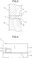
- FIG. 3 is a cross-sectional view of a bonding layer and its surroundings of the imaging apparatus of the first embodiment
- FIG. 4 is a rear view of the imaging apparatus of the first embodiment
- FIG. 5 is an exploded, perspective view of an imaging apparatus in accordance with a second embodiment of the present disclosure.
- FIG. 6 is a cross-sectional view of the imaging apparatus of the second embodiment
- FIG. 7 is an example of assembling a first housing member and a second housing member together
- FIG. 8 is another example of assembling a first housing member and a second housing member together.
- FIG. 9 is another example of assembling a first housing member and a second housing member together.
- FIGS. 1 and 2 A configuration of an imaging apparatus 1 in accordance with a first embodiment of the present disclosure will now be described with reference to FIGS. 1 and 2 .
- the imaging apparatus 1 is installed inside a windshield of a vehicle to capture images in the forward direction of the vehicle.
- the term “vertical direction” for each member of the imaging apparatus 1 refers to a vertical direction of the member in a state where the imaging apparatus 1 is installed inside the windshield.
- the imaging apparatus 1 includes a housing 5 and an imaging module 30 .
- the imaging apparatus 1 has a cavity 4 within the housing 5 .
- the cavity 4 as shown in FIG. 2 , contains a main circuit board 40 .
- the housing 5 includes a first housing member 10 , a second housing member 20 , and a bonding member 3 .
- the housing 5 is an assembly of the first housing member 10 and the second housing member 20 .
- Each of the first housing member 10 and the second housing member 20 is an electrical conductor. More specifically, each of the first housing member 10 and the second housing member 20 is formed of an aluminum-based material, such as an aluminum alloy.
- the first housing member 10 has a first opening 11 .
- the first opening 11 has a first opening perimeter 11 a that is a perimeter of the first opening 11 .
- a first facing surface 12 of the first housing member 10 is provided circumferentially along the first opening perimeter 11 a of the first opening 11 .
- the second housing member 20 is disposed so as to cover the first opening 11 of the first housing member 10 . More specifically, the second housing member 20 has a second opening 21 facing the first opening 11 .
- the second opening 21 has a second opening perimeter 21 a that is a perimeter of the second opening 21 .
- a second facing surface 22 of the second housing member 20 is provided circumferentially along the second opening perimeter 21 a of the second opening 21 .
- the first housing member 10 and the second housing member are assembled to form the housing 5 with the first facing surface 12 of the first housing member 10 and the second facing surface 22 of the second housing member 20 facing each other on the perimeter of the second opening 21 .
- a connector aperture 15 is formed on the rear surface of the first housing member 10 .
- the connector aperture 15 has a generally rectangular shape such that part of the first opening perimeter 11 a corresponding to the lower side of the rectangle is cut out. Therefore, the first facing surface 12 is formed on a portion of the first opening perimeter 11 a excluding the part where the connector aperture 15 is formed.
- the second facing surface 22 of the second housing member 20 is formed on the entire second opening perimeter 21 a .
- the first housing member 10 and the second housing member 20 are assembled to form the housing 5 with the first facing surface 12 and the second facing surface 22 facing each other and with a portion of the second facing surface 22 excluding the part where the connector aperture 15 of the first housing member 10 is formed facing the first facing surface 12 .
- the connector aperture 15 may be formed anywhere on the housing 5 .
- the connector aperture 15 may be formed on the rear surface of the first housing member 10 and above the first opening perimeter 11 a .
- the first facing surface 12 may be formed throughout the entire first opening perimeter 11 a , such that the first facing surface 12 and the second facing surface 22 face each other throughout the entire perimeter of the first opening 11 and the second opening 21 .
- the bonding member 3 is an electrically conductive member interposed between the first housing member 10 and the second housing member 20 to close off a gap therebetween and electrically connect the first housing member 10 and the second housing member 20 .
- the bonding member 3 is interposed between the first facing surface 12 of the first housing member 10 and the second facing surface 22 of the second housing member 20 throughout the entire perimeter of the first facing surface 12 and the second facing surface 22 .
- the bonding member 3 has a thin tape shape, as a whole, a rectangle ring shape.
- the bonding member 3 is adhered to the first facing surface 12 and the second facing surface 22 and electrically connects the first housing member 10 and the second housing member 20 .
- the first housing member 10 and the second housing member 20 may be coupled in series.
- each of the first facing surface 12 and the second facing surface 22 faces and adheres to the bonding member 3 throughout its entire perimeter.
- An external connector 43 is received into the connector aperture 15 that is formed in the rear surface of the first housing member 10 to close off the connector aperture 15 .
- the external connector 43 is positioned such that its rear end face lies flush with the rear surface of the first housing member 10 . As shown in FIG. 4 , at least part of a surface of the bonding member 3 , facing the first housing member 10 , adheres to a bottom surface of the external connector 43 .
- a diagonal length of the connector aperture 15 is equal to or less than ⁇ /2.
- ⁇ is a wavelength of a highest frequency signal among various signals used in vehicle mounted devices.
- a frequency band of signals used in a vehicle mounted device for vehicle-to-infrastructure communications is a highest frequency band for vehicle use, including, for example, 2.5 GHz where ⁇ /2 is about 60 mm.
- the diagonal length of the connector aperture 15 set equal to or less than ⁇ /2. Even if there is a gap between the connector aperture 15 and the external connector 43 or between the external connector 43 and the bonding member 3 , not only leakage of electromagnetic waves of wavelength greater than ⁇ out of the housing 5 through the gap, but also ingress of external electromagnetic waves of greater wavelength than A into the housing 5 through the gap can be prevented.
- the bonding member 3 may be any type of electrically conductive member that can electrically connect the first housing member 10 and the second housing member 20 .
- the bonding member 3 includes an adhesive.
- the bonding member 3 itself has an adhesive property. Therefore, a surface of the bonding member 3 , facing the first facing surface 12 , can be adhered to the first facing surface 12 with sufficient adherence. Another surface of the bonding member 3 , facing the second facing surface 22 , is also adhered to the second facing surface 22 with sufficient adherence.
- the bonding member 3 may be a soft member or a hard member.
- the bonding member 3 may be a member that is soft or in paste form in its initial state and then harden under heat or over time.
- the first facing surface 12 of the first housing member 10 is adhered to the bonding member 3 throughout the entire opening perimeter 11 a
- the second facing surface 22 of the second housing member 20 is adhered to the bonding member 3 throughout the entire opening perimeter 21 a , whereby a gap between the first facing surface 12 of the first housing member 10 and the second facing surface 22 of the second housing member 20 is closed off by the bonding member 3 .
- Leakage of electromagnetic waves generated by components inside the housing 5 out of the housing 5 can be prevented. Ingress of external electromagnetic waves into the housing 5 can also be prevented.
- the imaging module 30 is configured to capture forward images of the vehicle and output image signals representing the captured forward images.
- the imaging module 30 includes a lens 31 and an imaging substrate 32 .
- the imaging substrate 32 is provided with a light receiving element (not shown).
- the housing 5 has a lens aperture 14 .
- the imaging module 30 is contained within a cavity 4 of the housing 5 .
- Part of the lens 31 is exposed externally of the housing 5 through the lens aperture 14 .
- At least one component of the imaging module 30 may be exposed externally of the housing 5 .
- the entire imaging module 30 may be contained within the housing 5 , where, for example, the housing 5 may include a transparent portion proximate the lens 31 such that light may be incident on the lens 31 through the transparent portion of the housing 5 .
- a longitudinal direction refers to a direction in which part of the imaging module 30 is exposed from the lens aperture 14 .
- lateral direction refer to a lateral direction of the imaging apparatus 1 as viewed from the imaging apparatus 1 looking forward.
- the imaging apparatus 1 may be installed such that the forward direction and the travel direction of the vehicle coincide.
- the light from an imaging target is incident on the lens 31 .
- the light from the imaging target travels to a light receiving element via the lens 31 and received by the light receiving element.
- the light receiving element outputs a signal responsive to the received light.
- the light receiving element may be a semiconductor image sensor element, such as a complementary metal-oxide semiconductor (CMOS) image sensor or the like.
- CMOS complementary metal-oxide semiconductor
- a signal output circuit is provided on the imaging substrate 32 .
- the signal output circuit is configured to output an image signal representing an image of the imaging target based on the light incident on the lens 31 , more specifically, based on a signal output from the light receiving element.
- the image signal output from the imaging module 30 is input to the main circuit board 40 .
- the main circuit board 40 includes a signal processing circuit 42 and the external connector 43 .
- the signal processing circuit 42 as a signal processor, processes image signals output from the imaging module 30 .
- the external connector 43 inputs external signals to the signal processing circuit 42 and outputs processing results of the signal processing circuit 42 .
- the first housing member 10 has four screw holes 10 a , 10 b , 10 c , 10 d , to join the first housing member 10 and the second housing member 20 together.
- the second housing member 20 has four through holes 20 a , 20 b , 20 c , 20 d positioned opposite the respective screw holes 10 a , 10 b , 10 c , 10 d , to join the second housing member 20 and the first housing member 10 together.
- the first housing member 10 and the second housing member 20 are not only joined adhesively by the bonding member 3 , but also secured mechanically by the four screws 28 as fasteners.
- the assembling procedure of the housing 5 is as follows.
- the bonding member 3 is applied to the first facing surface 12 of the first housing member 10 or the second facing surface 22 of the second housing member 20 , whereby the bonding member 3 is adhered to the first facing surface 12 of the first housing member 10 or the second facing surface 22 of the second housing member 20 .
- first housing member 10 and the second housing member 20 are combined such that the facing surfaces 12 , 22 face each other, whereby the first facing surface 12 and the second facing surface 22 are both adhered to the bonding member 3 .
- the bonding member 3 undergoes a thermal hardening treatment.
- the bonding member 3 is heated to be thermally hardened.
- the bonding member 3 is hardened over time.
- Each of members including the main circuit board 40 to be contained within the cavity 4 of the housing 5 may be placed in either one of the first housing member 10 and the second housing member 20 before the first housing member 10 and the second housing member 20 are assembled together to form the housing 5 .
- the first housing member 10 and the second housing member 20 are joined together by the bonding member 3 therebetween, the first housing member 10 and the second housing member 20 are secured to each other with four screws 28 . That is, the four screws 28 are inserted into the respective screw holes 10 a , 10 b , 10 c , 10 d through the through holes 20 a , 20 b , 20 c , 20 d of the second housing member 20 .
- the first embodiment can provide advantages (1a)-(1d).
- the housing 5 of the imaging apparatus 1 includes the first housing member 10 and the second housing member 20 .
- the first housing member 10 and the second housing member 20 are joined and electrically connected by the electrically conductive bonding member 3 therebetween. Leakage of electromagnetic waves generated by components inside the housing 5 out of the housing 5 and ingress of external electromagnetic waves into the housing 5 can be prevented.
- the bonding member 3 is interposed between the first facing surface 12 of the first housing member 10 and the second facing surface 22 of the second housing member 20 throughout the entire perimeter of the first facing surface 12 and the second facing surface 22 .
- the bonding member 3 is adhered to the first facing surface 12 and the second facing surface 22 throughout the entire perimeter of the first facing surface 12 and the second facing surface 22 , which can prevent leakage of electromagnetic waves out of the housing 5 and ingress of external electromagnetic waves into the housing 5 .
- the bonding member 3 itself has an adhesive property and can be adhered to the first facing surface 12 and the second facing surface 22 .
- This configuration can increase adhesion of the first facing surface 12 and the second facing surface 22 to the bonding member 3 , and is therefore less prone to gap generation between first facing surface 12 and the second facing surface 22 .
- first housing member 10 and the second housing member 20 are mechanically secured to each other by a plurality of screws 28 .
- This configuration can increase adhesion of the first facing surface 12 and the second facing surface 22 to the bonding member 3 .
- the imaging apparatus 50 includes a housing 55 , an imaging module 80 , and a main circuit board 90 .
- the housing 55 includes a first housing member 60 and a second housing member 70 .
- Each of the first housing member 60 and the second housing member 70 is an electrical conductor.
- the housing 55 is an assembly of the first housing member 60 and the second housing member 70 .
- the imaging module 80 and the main circuit board 90 are contained in a cavity 54 of the housing 55 .
- the first housing member 60 differs from the first housing member 10 of the first embodiment only in the shape of the first facing surface.
- the first housing member 60 includes a first opening 61 and a first opening perimeter 61 a that is a perimeter of the first opening 61 .
- the first facing surface 62 is provided throughout the entire first opening perimeter 61 a .
- the first housing member 60 has a lens aperture 64 .
- the second housing member 70 also differs from the second housing member 20 of the first embodiment only in the shape of the second facing surface.
- the second housing member 70 includes a second opening 71 and a second opening perimeter 71 a that is a perimeter of the second opening 71 .
- the second facing surface 72 is provided throughout the entire second opening perimeter 71 a .
- the first housing member 60 has a lens aperture 64 .
- each of the first facing surface 62 and the second facing surface 72 has an L-shaped cross-section perpendicular to the circumferential direction.
- a bonding member 100 is interposed between the first facing surface 62 and the second facing surface 72 .
- the bonding member 100 has an adhesive and electrically conductive property and disposed to face the first facing surface 62 and the second facing surface 72 throughout the entire perimeter of the first facing surface 62 and the second facing surface 72 .
- the bonding member 100 adheres to and electrically connects the first facing surface 62 and the second facing surface 72 .
- the bonding member 100 is initially in paste form and is then thermally hardened. That is, the bonding member 100 , as a whole, is an electrically conductive adhesive.
- first housing member 60 and the second housing member 70 are also secured to each other by a plurality of screws as in the first embodiment.
- the imaging module 80 includes a lens 81 and an imaging substrate 82 .
- the lens 81 is similar to the lens 31 of the first embodiment.
- the imaging substrate 82 is similar to the imaging substrate 32 of the first embodiment.
- the imaging module 80 is contained within the cavity 54 of the housing 55 .
- Part of the lens 81 is exposed externally of the housing 55 from the lens aperture 44 .
- the imaging module 80 further includes a cable 83 and a module connector 84 .
- the cable 83 may be a flat-type cable such that a plurality of flat cables are arranged in a generally co-planar fashion. Image signals generated in the signal output circuit of the imaging substrate 82 is transmitted to the module connector 84 via the cable 83 , and in turn, output from the module connector 84 .
- the main circuit board 90 includes a signal processing circuit 92 and an external connector 93 .
- the signal processing circuit 92 and the external connector 93 are respectively similar in both configuration and function to the signal processing circuit 42 and the external connector 43 of the first embodiment.
- Part of the signal processing circuit 92 and the external connector 93 are provided on an upper board surface of the main circuit board 90 .
- a board connector 96 is provided on a lower board surface of the main circuit board 90 .
- the board connector 96 is electrically connected to the signal processing circuit 92 .
- the board connector 96 is mated with the module connector 84 of the imaging module 80 . That is, the main circuit board 90 is electrically connected to the imaging module 80 through the imaging substrate 82 , the board connector 96 , and the module connector 84 , such that various signals are transmitted and received between the main circuit board 90 and the imaging module 80 .
- the main circuit board 90 has an aperture 94 therethrough. Part of the imaging module 80 is inserted inside the aperture 94 of the main circuit board 90 . In present embodiment, as shown in FIG. 6 , the imaging module 80 is disposed with part of the imaging substrate 82 inserted inside the aperture 94 of the main circuit board 90 .
- the majority of the imaging module 80 excluding part thereof is disposed on a top side of the main circuit board 90 .
- the board connector 96 is disposed on a bottom side of the main circuit board 90 . In such a positional relationship, as shown in FIG. 6 , the imaging module 80 is connected to the board connector 96 of the main circuit board 90 via the aperture 94 .
- Which part of the imaging module 80 is placed inside the aperture 94 of the main circuit board 90 may suitably be determined.
- the entire imaging substrate 82 may be disposed on the top side of the main circuit board 90 , and the cable 83 may be disposed to pass through the aperture 94 of the main circuit board 90 .
- the assembling procedure of the housing 55 may be as follows.
- the paste-like bonding member 100 is applied to either one of the first facing surface 62 of the first housing member 60 and the second facing surface 72 of the second housing member 70 .
- first housing member 60 and the second housing member 70 are combined such that the first facing surface 62 and the second facing surface 72 face each other, such that the first facing surface 62 and the second facing surface 72 are both adhered to the bonding member 100 .
- a thermal hardening treatment is applied to the bonding member 100 .
- the first housing member 60 and the second housing member 70 are secured to each other by a plurality of screws (not shown).
- the second embodiment set forth above in detail can provide not only the advantages (1a)-(1d) of the first embodiment, but also the following advantages.
- first facing surface 62 and the second facing surface 72 have an L-shaped cross-section perpendicular to the circumferential direction. Therefore, in the assembling procedure, the proper, horizontal, relative positional relationship between the first housing member 60 and the second housing member 70 can readily be achieved. Even after completion of the assembling procedure, the horizontal, relative positional relationship can properly be maintained without using the screws.
- the first facing surface and the second facing surface have a flat shape in the first embodiment.
- the first facing surface and the second facing surface have an L-shaped cross-section in the second embodiment.
- the first facing surface and the second facing surface have a different shape.
- a groove having an arc-like cross-section may circumferentially be formed on at least one of the first facing surface and the second facing surface.
- a ring-shaped bonding member may be laid in the groove, whereby the first facing surface and the second facing surface are adhered to each other with the bonding member interposed therebetween.
- a rib-shaped protrusion may circumferentially be formed on one of the first facing surface and the second facing surface, and a groove may be formed on the other of the first facing surface and the second facing surface, such that the rib-shaped protrusion is inserted inside the groove with the bonding member filled in the groove.
- FIGS. 7 and 8 illustrates an example.
- FIG. 7 illustrates an example of the imaging apparatus, where a rib protrusion 123 is circumferentially formed on the first facing surface 122 of the first housing member 120 and a groove 133 is circumferentially formed on the second facing surface 132 of the second housing member 130 .
- the protrusion 123 of the first housing member 120 protrudes toward the second facing surface 132 .
- the groove 133 of the second facing surface 132 is positioned opposite the protrusion 123 to be inserted into the protrusion 123 with the bonding member 140 filled in the groove 133 .
- a procedure of assembling the first housing member 120 and the second housing member 130 to form the imaging apparatus is as follows. As shown at the top of FIG. 7 , the first housing member 120 and the second housing member 130 are spaced apart from each other in a not yet assembled state.
- a paste-like, soft bonding member 140 is filled in the groove 133 of the second housing member 130 .
- the first housing member 120 is put onto the second housing member 130 such that the protrusion 123 of the first housing member 120 is inserted into the groove 133 of the second housing member 130 .
- the protrusion 123 of the first housing member 120 After insertion of the protrusion 123 of the first housing member 120 into the groove 133 of the second housing member 130 , the protrusion 123 of the first housing member 120 is embedded in the bonding member 140 filled in the groove 133 , as shown in the bottom of FIG. 7 .
- the bonding member 140 is filled in the groove 133 to completely close the groove 133 . Therefore, as shown in the bottom of FIG. 7 , as the protrusion 123 is inserted into the groove 133 , part of the bonding member 140 will run out of the groove 133 .
- a thermal hardening treatment is applied to the bonding member 140 with at least part of the protrusion 123 inserted inside the groove 133 as shown in the bottom of FIG. 7 .
- the protrusion 123 may be inserted into the groove 133 until the tip of the protrusion 123 reaches the bottom of the groove 133 or until the first facing surface 122 gets in contact with the second facing surface 132 .
- FIG. 8 illustrates another example of the imaging apparatus, where a second facing surface 162 of a second housing member 160 has an L-shaped cross-section as in the second embodiment, and a groove 153 is circumferentially formed on a first facing surface 152 of a first housing member 150 .
- a second facing surface 162 of a second housing member 160 has an L-shaped cross-section as in the second embodiment, and a groove 153 is circumferentially formed on a first facing surface 152 of a first housing member 150 .
- a procedure of assembling the first housing member 150 and the second housing member 160 to form the imaging apparatus is as follows. First, a paste-like, soft bonding member 170 is filled in the groove 153 of the first housing member 150 . After filling the groove 153 with the bonding member 170 , the first housing member 150 is put onto the second housing member 160 such that at least part of the protrusion 163 of the second housing member 160 is inserted inside the groove 153 of the first housing member 150 .
- the protrusion 153 of the second housing member 160 is embedded in the bonding member 170 filled in the groove 153 , as shown in the bottom of FIG. 8 .
- part of the bonding member 170 may run out of the groove 153 .
- a thermal hardening treatment is applied to the bonding member 170 with at least part of the protrusion 163 inserted inside the groove 153 as shown in FIG. 8 .
- each facing surface is provided throughout the entire opening perimeter. In an alternative embodiment, each facing surface may not be provided throughout the entire opening perimeter. In the embodiments set forth above, the bonding member is provided throughout the entire opening perimeter. In an alternative embodiment, the bonding member may not be provided throughout the entire opening perimeter. For example, the bonding member may be provided between the first facing surface and the second facing surface only along part of the opening perimeter. For example, the bonding member may be provided between the first facing surface and the second facing surface such that there are one or more spaces free from the bonding member between the first facing surface and the second facing surface.
- the bonding member may be provided between the first facing surface and the second facing surface such that any space free from the bonding member between the first facing surface and the second facing surface has a circumferential length of less than one-half of a signal wavelength, that is, ⁇ /2 as set forth above.
- the bonding member has an adhesive property.
- the bonding member may have no adhesive property to both the first facing surface and the second facing surface.
- the bonding member may have an adhesive property to one of the first facing surface and the second facing surface, and the bonding member may only have to be in intimate contact with the other of the first facing surface and the second facing surface.
- the bonding member as a whole has an adhesive property.
- the bonding member may not have an adhesive property as a whole, or the bonding member may have a laminated structure formed of a plurality of layers.
- the bonding member may have a laminated structure formed of a layer including no adhesive or a low adhesive content, and an adhesive-based layer.
- FIG. 9 illustrates an example of such a laminated structure of the bonding member as an alternative to the bonding member 3 of the imaging apparatus 1 of the first embodiment.
- the bonding member 200 has a laminated structure.
- the bonding member 200 shown in FIG. 9 is formed of an interlayer 201 , a first adhesive layer 202 , and a second adhesive layer 203 .
- Each of the interlayer 201 , the first bonding layer 202 , and the second bonding layer 203 is an electrically conductive member.
- the interlayer 201 may have no adhesive property or a low adhesive content.
- Each of the first adhesive layer 202 and the second adhesive layer 203 has an adhesive with a higher adhesive property than the interlayer 201 .
- the first adhesive layer 202 is in contact with and adhered to the first facing surface, thereby causing the interlayer 201 to adhere to the first facing surface.
- the first adhesive layer 202 causes the bonding member to adhere to the first facing surface.
- the second adhesive layer 203 is in contact with and adhered to the second facing surface, thereby causing the interlayer 201 to adhere to the second facing surface.
- the second adhesive layer 203 causes the bonding member to adhere to the second facing surface.
- either one of the first adhesive layer 202 and the second adhesive layer 203 may be removed.
- the interlayer 201 may also have an adhesive property.
- the interlayer 201 may be formed of the same material as the bonding member 3 of the first embodiment.
- each of the bonding members 3 , 100 as a whole is an adhesive layer with an adhesive property.
- screws 28 are used as fasteners.
- the number of screws is not limited to four.
- the number of screws may be greater or less than four.
- positions of the fasteners may be arbitrarily determined.
- Fasteners other than screws may be used to mechanically secure the first housing member and the second housing member to each other.
- crimp engagement or snap fit engagement may be applied to secure the first housing member and the second housing member to each other at at least one portion of the at least one portion along the perimeter of the opening of each of the first and second housing members.
- the bonding member only has to have an adhesive property, where both the first and second housing members may be secured only with the adhesive property of the bonding member, without using fasteners, such as screws.
- the imaging apparatus includes only one imaging module.
- the imaging apparatus may include a plurality of imaging modules.
- first housing member and the second housing member are formed of an aluminum-based material.
- first housing member and the second housing member may be formed of another-metal-based material other than the aluminum-based material.
- the functions of a single component may be distributed to a plurality of components, or the functions of a plurality of components may be integrated into a single component.
- At least part of the configuration of the above embodiments may be replaced with a known configuration having a similar function.
- At least part of the configuration of the above embodiments may be removed.
- At least part of the configuration of one of the above embodiments may be replaced with or added to the configuration of another one of the above embodiments.
Landscapes
- Engineering & Computer Science (AREA)
- Multimedia (AREA)
- Signal Processing (AREA)
- Microelectronics & Electronic Packaging (AREA)
- Mechanical Engineering (AREA)
- Physics & Mathematics (AREA)
- Electromagnetism (AREA)
- Studio Devices (AREA)
- Details Of Cameras Including Film Mechanisms (AREA)
- Accessories Of Cameras (AREA)
- Shielding Devices Or Components To Electric Or Magnetic Fields (AREA)
Abstract
Description
Claims (12)
Applications Claiming Priority (2)
| Application Number | Priority Date | Filing Date | Title |
|---|---|---|---|
| JP2017-173917 | 2017-09-11 | ||
| JP2017173917A JP7059541B2 (en) | 2017-09-11 | 2017-09-11 | Imaging device |
Publications (2)
| Publication Number | Publication Date |
|---|---|
| US20190082082A1 US20190082082A1 (en) | 2019-03-14 |
| US10812688B2 true US10812688B2 (en) | 2020-10-20 |
Family
ID=65441505
Family Applications (1)
| Application Number | Title | Priority Date | Filing Date |
|---|---|---|---|
| US16/127,683 Active US10812688B2 (en) | 2017-09-11 | 2018-09-11 | Imaging apparatus |
Country Status (4)
| Country | Link |
|---|---|
| US (1) | US10812688B2 (en) |
| JP (1) | JP7059541B2 (en) |
| CN (1) | CN109495674B (en) |
| DE (1) | DE102018215391A1 (en) |
Families Citing this family (2)
| Publication number | Priority date | Publication date | Assignee | Title |
|---|---|---|---|---|
| JP7407017B2 (en) * | 2020-02-28 | 2023-12-28 | 株式会社東海理化電機製作所 | Installation equipment |
| DE102020108771A1 (en) | 2020-03-30 | 2021-09-30 | Connaught Electronics Ltd. | Method for assembling a camera for a vehicle, pre-assembly module for a camera and camera |
Citations (11)
| Publication number | Priority date | Publication date | Assignee | Title |
|---|---|---|---|---|
| JPS60166197A (en) | 1984-02-08 | 1985-08-29 | Ihara Chem Ind Co Ltd | Screw Press |
| JP2007274624A (en) | 2006-03-31 | 2007-10-18 | Citizen Miyota Co Ltd | Camera module |
| US20090223711A1 (en) | 2008-03-06 | 2009-09-10 | Yoshikazu Ueno | Shield method for electronic component enclosure and shield material |
| JP2012047816A (en) | 2010-08-24 | 2012-03-08 | Sharp Corp | Camera module, and method of manufacturing the same |
| WO2013123161A1 (en) | 2012-02-17 | 2013-08-22 | Magna Electronics, Inc. | Vehicle vision system with light baffling system |
| US20140132768A1 (en) * | 2012-11-15 | 2014-05-15 | Samsung Electro-Mechanics Co., Ltd. | Camera for car |
| US20150015713A1 (en) | 2011-08-02 | 2015-01-15 | Magma Electronics Inc. | Vehicle vision system with light baffling system |
| US20150281528A1 (en) * | 2014-03-26 | 2015-10-01 | Hong Fu Jin Precision Industry (Shenzhen) Co., Ltd. | Camera module |
| US20150327398A1 (en) * | 2014-05-09 | 2015-11-12 | Magna Electronics Inc. | Vehicle vision system with forward viewing camera |
| US20160307953A1 (en) * | 2015-04-16 | 2016-10-20 | Denso Corporation | Imaging device and circuit board therefor |
| US20180148000A1 (en) * | 2016-11-29 | 2018-05-31 | Denso Corporation | Imaging apparatus |
Family Cites Families (13)
| Publication number | Priority date | Publication date | Assignee | Title |
|---|---|---|---|---|
| JPH0488099U (en) * | 1990-12-17 | 1992-07-30 | ||
| JPH11239288A (en) * | 1998-02-20 | 1999-08-31 | Fuji Heavy Ind Ltd | Case body structure for video camera |
| JP4900118B2 (en) * | 2007-07-31 | 2012-03-21 | コニカミノルタオプト株式会社 | Camera module and electronic equipment |
| JP5494927B2 (en) * | 2009-08-03 | 2014-05-21 | 株式会社リコー | Camera unit and sensing device |
| KR20110063158A (en) * | 2009-12-04 | 2011-06-10 | 삼성전기주식회사 | Camera module |
| US8717495B2 (en) * | 2010-04-16 | 2014-05-06 | Panasonic Corporation | Digital camera |
| CN102331612A (en) * | 2010-07-13 | 2012-01-25 | 鸿富锦精密工业(深圳)有限公司 | Lens module and portable electronic device using the lens module |
| JP2012113186A (en) * | 2010-11-26 | 2012-06-14 | Mitsumi Electric Co Ltd | Camera module |
| EP2696575B1 (en) * | 2011-04-05 | 2018-10-10 | Panasonic Intellectual Property Management Co., Ltd. | Solid-state image pickup device, and method for manufacturing solid-state image pickup device |
| KR101428842B1 (en) * | 2011-11-08 | 2014-08-08 | 엘지이노텍 주식회사 | Camera module for Vehicle |
| KR101952853B1 (en) * | 2013-07-12 | 2019-02-27 | 삼성전기주식회사 | Camera module |
| KR102248085B1 (en) * | 2014-10-17 | 2021-05-04 | 엘지이노텍 주식회사 | Camera module using for automobile |
| DE102015110262A1 (en) * | 2015-06-25 | 2016-12-29 | Connaught Electronics Ltd. | Camera for a motor vehicle with shielding device, driver assistance system and motor vehicle |
-
2017
- 2017-09-11 JP JP2017173917A patent/JP7059541B2/en active Active
-
2018
- 2018-09-11 DE DE102018215391.4A patent/DE102018215391A1/en active Pending
- 2018-09-11 CN CN201811057532.3A patent/CN109495674B/en active Active
- 2018-09-11 US US16/127,683 patent/US10812688B2/en active Active
Patent Citations (13)
| Publication number | Priority date | Publication date | Assignee | Title |
|---|---|---|---|---|
| JPS60166197A (en) | 1984-02-08 | 1985-08-29 | Ihara Chem Ind Co Ltd | Screw Press |
| JP2007274624A (en) | 2006-03-31 | 2007-10-18 | Citizen Miyota Co Ltd | Camera module |
| US20090223711A1 (en) | 2008-03-06 | 2009-09-10 | Yoshikazu Ueno | Shield method for electronic component enclosure and shield material |
| JP2009212446A (en) | 2008-03-06 | 2009-09-17 | Smk Corp | Shield method for electronic component enclosure and shield member |
| JP2012047816A (en) | 2010-08-24 | 2012-03-08 | Sharp Corp | Camera module, and method of manufacturing the same |
| US20150015713A1 (en) | 2011-08-02 | 2015-01-15 | Magma Electronics Inc. | Vehicle vision system with light baffling system |
| WO2013123161A1 (en) | 2012-02-17 | 2013-08-22 | Magna Electronics, Inc. | Vehicle vision system with light baffling system |
| US20140132768A1 (en) * | 2012-11-15 | 2014-05-15 | Samsung Electro-Mechanics Co., Ltd. | Camera for car |
| US20150281528A1 (en) * | 2014-03-26 | 2015-10-01 | Hong Fu Jin Precision Industry (Shenzhen) Co., Ltd. | Camera module |
| US20150327398A1 (en) * | 2014-05-09 | 2015-11-12 | Magna Electronics Inc. | Vehicle vision system with forward viewing camera |
| US20160307953A1 (en) * | 2015-04-16 | 2016-10-20 | Denso Corporation | Imaging device and circuit board therefor |
| US20180148000A1 (en) * | 2016-11-29 | 2018-05-31 | Denso Corporation | Imaging apparatus |
| JP2018087916A (en) | 2016-11-29 | 2018-06-07 | 株式会社デンソー | Imaging device |
Also Published As
| Publication number | Publication date |
|---|---|
| CN109495674A (en) | 2019-03-19 |
| JP2019050506A (en) | 2019-03-28 |
| CN109495674B (en) | 2021-05-07 |
| US20190082082A1 (en) | 2019-03-14 |
| JP7059541B2 (en) | 2022-04-26 |
| DE102018215391A1 (en) | 2019-03-14 |
Similar Documents
| Publication | Publication Date | Title |
|---|---|---|
| JP7741245B2 (en) | Automotive Camera Assembly | |
| JP6721745B2 (en) | Imaging device and vehicle | |
| US7268957B2 (en) | Optical module and optical system | |
| JP3836235B2 (en) | Solid-state imaging device and manufacturing method thereof | |
| US9179053B2 (en) | Solid-state imaging apparatus and method of producing a solid-state imaging apparatus | |
| US9019421B2 (en) | Method of manufacturing a miniaturization image capturing module | |
| US8605211B2 (en) | Low rise camera module | |
| US7521790B2 (en) | Semiconductor device module and manufacturing method of semiconductor device module | |
| WO2013118501A1 (en) | Imaging unit and imaging apparatus | |
| US9345134B2 (en) | Printed wiring board | |
| JP6732438B2 (en) | Imaging device | |
| US10732488B2 (en) | Holder assembly for camera module, camera module having same, and waterproof connector | |
| US10812688B2 (en) | Imaging apparatus | |
| US9491848B2 (en) | Grounding part, electronic device, imaging device, and grounding part production method | |
| JP4031104B2 (en) | Stereo camera | |
| KR101038492B1 (en) | Camera module and its manufacturing method | |
| JPH104510A (en) | camera | |
| US11765448B2 (en) | Electronic component including electronic substrate and circuit member, apparatus, and camera | |
| US20250142193A1 (en) | Camera device | |
| JPH02150177A (en) | video camera equipment | |
| KR102726703B1 (en) | Camera | |
| KR20190025331A (en) | Camera module | |
| JP2003065845A (en) | Infrared detector | |
| KR20080015257A (en) | Camera module and its manufacturing method | |
| CN102202184B (en) | Photoelectric conversion element unit and imaging device |
Legal Events
| Date | Code | Title | Description |
|---|---|---|---|
| FEPP | Fee payment procedure |
Free format text: ENTITY STATUS SET TO UNDISCOUNTED (ORIGINAL EVENT CODE: BIG.); ENTITY STATUS OF PATENT OWNER: LARGE ENTITY |
|
| AS | Assignment |
Owner name: DENSO CORPORATION, JAPAN Free format text: ASSIGNMENT OF ASSIGNORS INTEREST;ASSIGNOR:HASHIMOTO, MARIE;REEL/FRAME:047369/0330 Effective date: 20180920 |
|
| STPP | Information on status: patent application and granting procedure in general |
Free format text: DOCKETED NEW CASE - READY FOR EXAMINATION |
|
| STPP | Information on status: patent application and granting procedure in general |
Free format text: NON FINAL ACTION MAILED |
|
| STPP | Information on status: patent application and granting procedure in general |
Free format text: RESPONSE TO NON-FINAL OFFICE ACTION ENTERED AND FORWARDED TO EXAMINER |
|
| STPP | Information on status: patent application and granting procedure in general |
Free format text: FINAL REJECTION MAILED |
|
| STPP | Information on status: patent application and granting procedure in general |
Free format text: RESPONSE AFTER FINAL ACTION FORWARDED TO EXAMINER |
|
| STPP | Information on status: patent application and granting procedure in general |
Free format text: NOTICE OF ALLOWANCE MAILED -- APPLICATION RECEIVED IN OFFICE OF PUBLICATIONS |
|
| STPP | Information on status: patent application and granting procedure in general |
Free format text: AWAITING TC RESP., ISSUE FEE NOT PAID |
|
| STCF | Information on status: patent grant |
Free format text: PATENTED CASE |
|
| MAFP | Maintenance fee payment |
Free format text: PAYMENT OF MAINTENANCE FEE, 4TH YEAR, LARGE ENTITY (ORIGINAL EVENT CODE: M1551); ENTITY STATUS OF PATENT OWNER: LARGE ENTITY Year of fee payment: 4 |