US10790294B2 - Vertical memory device - Google Patents
Vertical memory device Download PDFInfo
- Publication number
- US10790294B2 US10790294B2 US15/465,355 US201715465355A US10790294B2 US 10790294 B2 US10790294 B2 US 10790294B2 US 201715465355 A US201715465355 A US 201715465355A US 10790294 B2 US10790294 B2 US 10790294B2
- Authority
- US
- United States
- Prior art keywords
- semiconductor patterns
- channel structures
- gate electrode
- insulating layer
- disposed
- Prior art date
- Legal status (The legal status is an assumption and is not a legal conclusion. Google has not performed a legal analysis and makes no representation as to the accuracy of the status listed.)
- Active, expires
Links
- 239000004065 semiconductor Substances 0.000 claims abstract description 144
- 239000000758 substrate Substances 0.000 claims abstract description 58
- 239000010410 layer Substances 0.000 claims description 313
- 239000011229 interlayer Substances 0.000 claims description 61
- 230000002093 peripheral effect Effects 0.000 claims description 34
- 239000000463 material Substances 0.000 abstract description 25
- 238000000034 method Methods 0.000 description 19
- 229910052814 silicon oxide Inorganic materials 0.000 description 10
- 229910052581 Si3N4 Inorganic materials 0.000 description 9
- 238000004891 communication Methods 0.000 description 9
- HQVNEWCFYHHQES-UHFFFAOYSA-N silicon nitride Chemical compound N12[Si]34N5[Si]62N3[Si]51N64 HQVNEWCFYHHQES-UHFFFAOYSA-N 0.000 description 9
- VYPSYNLAJGMNEJ-UHFFFAOYSA-N Silicium dioxide Chemical compound O=[Si]=O VYPSYNLAJGMNEJ-UHFFFAOYSA-N 0.000 description 8
- 238000005530 etching Methods 0.000 description 7
- 229910021420 polycrystalline silicon Inorganic materials 0.000 description 7
- 229910052751 metal Inorganic materials 0.000 description 6
- 239000002184 metal Substances 0.000 description 6
- 238000003860 storage Methods 0.000 description 6
- 230000015572 biosynthetic process Effects 0.000 description 5
- 239000012535 impurity Substances 0.000 description 5
- 230000005641 tunneling Effects 0.000 description 5
- XUIMIQQOPSSXEZ-UHFFFAOYSA-N Silicon Chemical compound [Si] XUIMIQQOPSSXEZ-UHFFFAOYSA-N 0.000 description 4
- 150000001875 compounds Chemical class 0.000 description 4
- 239000004020 conductor Substances 0.000 description 4
- 239000003989 dielectric material Substances 0.000 description 4
- 230000006870 function Effects 0.000 description 4
- 229910052710 silicon Inorganic materials 0.000 description 4
- 239000010703 silicon Substances 0.000 description 4
- WFKWXMTUELFFGS-UHFFFAOYSA-N tungsten Chemical compound [W] WFKWXMTUELFFGS-UHFFFAOYSA-N 0.000 description 4
- 229910052721 tungsten Inorganic materials 0.000 description 4
- 239000010937 tungsten Substances 0.000 description 4
- PXHVJJICTQNCMI-UHFFFAOYSA-N Nickel Chemical compound [Ni] PXHVJJICTQNCMI-UHFFFAOYSA-N 0.000 description 3
- 229910000577 Silicon-germanium Inorganic materials 0.000 description 3
- LEVVHYCKPQWKOP-UHFFFAOYSA-N [Si].[Ge] Chemical compound [Si].[Ge] LEVVHYCKPQWKOP-UHFFFAOYSA-N 0.000 description 3
- 230000000903 blocking effect Effects 0.000 description 3
- 238000005229 chemical vapour deposition Methods 0.000 description 3
- 238000009413 insulation Methods 0.000 description 3
- 238000004519 manufacturing process Methods 0.000 description 3
- 239000007769 metal material Substances 0.000 description 3
- TWNQGVIAIRXVLR-UHFFFAOYSA-N oxo(oxoalumanyloxy)alumane Chemical compound O=[Al]O[Al]=O TWNQGVIAIRXVLR-UHFFFAOYSA-N 0.000 description 3
- BASFCYQUMIYNBI-UHFFFAOYSA-N platinum Chemical compound [Pt] BASFCYQUMIYNBI-UHFFFAOYSA-N 0.000 description 3
- 238000000926 separation method Methods 0.000 description 3
- 229910021332 silicide Inorganic materials 0.000 description 3
- FVBUAEGBCNSCDD-UHFFFAOYSA-N silicide(4-) Chemical compound [Si-4] FVBUAEGBCNSCDD-UHFFFAOYSA-N 0.000 description 3
- 125000006850 spacer group Chemical group 0.000 description 3
- 229910021417 amorphous silicon Inorganic materials 0.000 description 2
- 238000010586 diagram Methods 0.000 description 2
- 230000010354 integration Effects 0.000 description 2
- 229910021421 monocrystalline silicon Inorganic materials 0.000 description 2
- 239000002159 nanocrystal Substances 0.000 description 2
- 150000004767 nitrides Chemical class 0.000 description 2
- SIWVEOZUMHYXCS-UHFFFAOYSA-N oxo(oxoyttriooxy)yttrium Chemical compound O=[Y]O[Y]=O SIWVEOZUMHYXCS-UHFFFAOYSA-N 0.000 description 2
- BPUBBGLMJRNUCC-UHFFFAOYSA-N oxygen(2-);tantalum(5+) Chemical compound [O-2].[O-2].[O-2].[O-2].[O-2].[Ta+5].[Ta+5] BPUBBGLMJRNUCC-UHFFFAOYSA-N 0.000 description 2
- RVTZCBVAJQQJTK-UHFFFAOYSA-N oxygen(2-);zirconium(4+) Chemical compound [O-2].[O-2].[Zr+4] RVTZCBVAJQQJTK-UHFFFAOYSA-N 0.000 description 2
- 238000000059 patterning Methods 0.000 description 2
- 239000002096 quantum dot Substances 0.000 description 2
- LIVNPJMFVYWSIS-UHFFFAOYSA-N silicon monoxide Chemical class [Si-]#[O+] LIVNPJMFVYWSIS-UHFFFAOYSA-N 0.000 description 2
- 229910001936 tantalum oxide Inorganic materials 0.000 description 2
- 239000010936 titanium Substances 0.000 description 2
- 229910001928 zirconium oxide Inorganic materials 0.000 description 2
- 229910052774 Proactinium Inorganic materials 0.000 description 1
- GWEVSGVZZGPLCZ-UHFFFAOYSA-N Titan oxide Chemical compound O=[Ti]=O GWEVSGVZZGPLCZ-UHFFFAOYSA-N 0.000 description 1
- RTAQQCXQSZGOHL-UHFFFAOYSA-N Titanium Chemical compound [Ti] RTAQQCXQSZGOHL-UHFFFAOYSA-N 0.000 description 1
- NRTOMJZYCJJWKI-UHFFFAOYSA-N Titanium nitride Chemical compound [Ti]#N NRTOMJZYCJJWKI-UHFFFAOYSA-N 0.000 description 1
- DBOSVWZVMLOAEU-UHFFFAOYSA-N [O-2].[Hf+4].[La+3] Chemical compound [O-2].[Hf+4].[La+3] DBOSVWZVMLOAEU-UHFFFAOYSA-N 0.000 description 1
- ILCYGSITMBHYNK-UHFFFAOYSA-N [Si]=O.[Hf] Chemical compound [Si]=O.[Hf] ILCYGSITMBHYNK-UHFFFAOYSA-N 0.000 description 1
- MIQVEZFSDIJTMW-UHFFFAOYSA-N aluminum hafnium(4+) oxygen(2-) Chemical compound [O-2].[Al+3].[Hf+4] MIQVEZFSDIJTMW-UHFFFAOYSA-N 0.000 description 1
- IVHJCRXBQPGLOV-UHFFFAOYSA-N azanylidynetungsten Chemical compound [W]#N IVHJCRXBQPGLOV-UHFFFAOYSA-N 0.000 description 1
- 229910017052 cobalt Inorganic materials 0.000 description 1
- 239000010941 cobalt Substances 0.000 description 1
- GUTLYIVDDKVIGB-UHFFFAOYSA-N cobalt atom Chemical compound [Co] GUTLYIVDDKVIGB-UHFFFAOYSA-N 0.000 description 1
- -1 for example Substances 0.000 description 1
- 229910052732 germanium Inorganic materials 0.000 description 1
- GNPVGFCGXDBREM-UHFFFAOYSA-N germanium atom Chemical compound [Ge] GNPVGFCGXDBREM-UHFFFAOYSA-N 0.000 description 1
- 229910052735 hafnium Inorganic materials 0.000 description 1
- VBJZVLUMGGDVMO-UHFFFAOYSA-N hafnium atom Chemical compound [Hf] VBJZVLUMGGDVMO-UHFFFAOYSA-N 0.000 description 1
- CJNBYAVZURUTKZ-UHFFFAOYSA-N hafnium(iv) oxide Chemical compound O=[Hf]=O CJNBYAVZURUTKZ-UHFFFAOYSA-N 0.000 description 1
- 239000011810 insulating material Substances 0.000 description 1
- 150000002500 ions Chemical class 0.000 description 1
- MRELNEQAGSRDBK-UHFFFAOYSA-N lanthanum(3+);oxygen(2-) Chemical compound [O-2].[O-2].[O-2].[La+3].[La+3] MRELNEQAGSRDBK-UHFFFAOYSA-N 0.000 description 1
- 229910052745 lead Inorganic materials 0.000 description 1
- 239000011859 microparticle Substances 0.000 description 1
- 238000010295 mobile communication Methods 0.000 description 1
- 238000012986 modification Methods 0.000 description 1
- 230000004048 modification Effects 0.000 description 1
- 229910052759 nickel Inorganic materials 0.000 description 1
- 230000003287 optical effect Effects 0.000 description 1
- 230000001590 oxidative effect Effects 0.000 description 1
- KJXBRHIPHIVJCS-UHFFFAOYSA-N oxo(oxoalumanyloxy)lanthanum Chemical compound O=[Al]O[La]=O KJXBRHIPHIVJCS-UHFFFAOYSA-N 0.000 description 1
- MMKQUGHLEMYQSG-UHFFFAOYSA-N oxygen(2-);praseodymium(3+) Chemical compound [O-2].[O-2].[O-2].[Pr+3].[Pr+3] MMKQUGHLEMYQSG-UHFFFAOYSA-N 0.000 description 1
- 229920002120 photoresistant polymer Polymers 0.000 description 1
- 229910052697 platinum Inorganic materials 0.000 description 1
- 238000005498 polishing Methods 0.000 description 1
- HBMJWWWQQXIZIP-UHFFFAOYSA-N silicon carbide Chemical compound [Si+]#[C-] HBMJWWWQQXIZIP-UHFFFAOYSA-N 0.000 description 1
- 229910010271 silicon carbide Inorganic materials 0.000 description 1
- 239000000126 substance Substances 0.000 description 1
- MZLGASXMSKOWSE-UHFFFAOYSA-N tantalum nitride Chemical compound [Ta]#N MZLGASXMSKOWSE-UHFFFAOYSA-N 0.000 description 1
- 229910052719 titanium Inorganic materials 0.000 description 1
- GFQYVLUOOAAOGM-UHFFFAOYSA-N zirconium(iv) silicate Chemical compound [Zr+4].[O-][Si]([O-])([O-])[O-] GFQYVLUOOAAOGM-UHFFFAOYSA-N 0.000 description 1
Images


Classifications
-
- H01L27/11568—
-
- H—ELECTRICITY
- H10—SEMICONDUCTOR DEVICES; ELECTRIC SOLID-STATE DEVICES NOT OTHERWISE PROVIDED FOR
- H10B—ELECTRONIC MEMORY DEVICES
- H10B41/00—Electrically erasable-and-programmable ROM [EEPROM] devices comprising floating gates
- H10B41/20—Electrically erasable-and-programmable ROM [EEPROM] devices comprising floating gates characterised by three-dimensional arrangements, e.g. with cells on different height levels
- H10B41/23—Electrically erasable-and-programmable ROM [EEPROM] devices comprising floating gates characterised by three-dimensional arrangements, e.g. with cells on different height levels with source and drain on different levels, e.g. with sloping channels
- H10B41/27—Electrically erasable-and-programmable ROM [EEPROM] devices comprising floating gates characterised by three-dimensional arrangements, e.g. with cells on different height levels with source and drain on different levels, e.g. with sloping channels the channels comprising vertical portions, e.g. U-shaped channels
-
- H01L27/11521—
-
- H01L27/11526—
-
- H01L27/11565—
-
- H01L27/1157—
-
- H01L27/11573—
-
- H01L27/11575—
-
- H01L27/11582—
-
- H—ELECTRICITY
- H10—SEMICONDUCTOR DEVICES; ELECTRIC SOLID-STATE DEVICES NOT OTHERWISE PROVIDED FOR
- H10B—ELECTRONIC MEMORY DEVICES
- H10B41/00—Electrically erasable-and-programmable ROM [EEPROM] devices comprising floating gates
- H10B41/30—Electrically erasable-and-programmable ROM [EEPROM] devices comprising floating gates characterised by the memory core region
-
- H—ELECTRICITY
- H10—SEMICONDUCTOR DEVICES; ELECTRIC SOLID-STATE DEVICES NOT OTHERWISE PROVIDED FOR
- H10B—ELECTRONIC MEMORY DEVICES
- H10B41/00—Electrically erasable-and-programmable ROM [EEPROM] devices comprising floating gates
- H10B41/40—Electrically erasable-and-programmable ROM [EEPROM] devices comprising floating gates characterised by the peripheral circuit region
-
- H—ELECTRICITY
- H10—SEMICONDUCTOR DEVICES; ELECTRIC SOLID-STATE DEVICES NOT OTHERWISE PROVIDED FOR
- H10B—ELECTRONIC MEMORY DEVICES
- H10B41/00—Electrically erasable-and-programmable ROM [EEPROM] devices comprising floating gates
- H10B41/50—Electrically erasable-and-programmable ROM [EEPROM] devices comprising floating gates characterised by the boundary region between the core region and the peripheral circuit region
-
- H—ELECTRICITY
- H10—SEMICONDUCTOR DEVICES; ELECTRIC SOLID-STATE DEVICES NOT OTHERWISE PROVIDED FOR
- H10B—ELECTRONIC MEMORY DEVICES
- H10B43/00—EEPROM devices comprising charge-trapping gate insulators
- H10B43/10—EEPROM devices comprising charge-trapping gate insulators characterised by the top-view layout
-
- H—ELECTRICITY
- H10—SEMICONDUCTOR DEVICES; ELECTRIC SOLID-STATE DEVICES NOT OTHERWISE PROVIDED FOR
- H10B—ELECTRONIC MEMORY DEVICES
- H10B43/00—EEPROM devices comprising charge-trapping gate insulators
- H10B43/20—EEPROM devices comprising charge-trapping gate insulators characterised by three-dimensional arrangements, e.g. with cells on different height levels
- H10B43/23—EEPROM devices comprising charge-trapping gate insulators characterised by three-dimensional arrangements, e.g. with cells on different height levels with source and drain on different levels, e.g. with sloping channels
- H10B43/27—EEPROM devices comprising charge-trapping gate insulators characterised by three-dimensional arrangements, e.g. with cells on different height levels with source and drain on different levels, e.g. with sloping channels the channels comprising vertical portions, e.g. U-shaped channels
-
- H—ELECTRICITY
- H10—SEMICONDUCTOR DEVICES; ELECTRIC SOLID-STATE DEVICES NOT OTHERWISE PROVIDED FOR
- H10B—ELECTRONIC MEMORY DEVICES
- H10B43/00—EEPROM devices comprising charge-trapping gate insulators
- H10B43/30—EEPROM devices comprising charge-trapping gate insulators characterised by the memory core region
- H10B43/35—EEPROM devices comprising charge-trapping gate insulators characterised by the memory core region with cell select transistors, e.g. NAND
-
- H—ELECTRICITY
- H10—SEMICONDUCTOR DEVICES; ELECTRIC SOLID-STATE DEVICES NOT OTHERWISE PROVIDED FOR
- H10B—ELECTRONIC MEMORY DEVICES
- H10B43/00—EEPROM devices comprising charge-trapping gate insulators
- H10B43/40—EEPROM devices comprising charge-trapping gate insulators characterised by the peripheral circuit region
-
- H—ELECTRICITY
- H10—SEMICONDUCTOR DEVICES; ELECTRIC SOLID-STATE DEVICES NOT OTHERWISE PROVIDED FOR
- H10B—ELECTRONIC MEMORY DEVICES
- H10B43/00—EEPROM devices comprising charge-trapping gate insulators
- H10B43/50—EEPROM devices comprising charge-trapping gate insulators characterised by the boundary region between the core and peripheral circuit regions
Definitions
- the present disclosure relates to a vertical memory device.
- An aspect of the present disclosure may provide a vertical memory device having improved reliability.
- a vertical memory device may include: a substrate having a cell array region and a connection region positioned on an exterior of the cell array region; a plurality of gate electrode layers stacked on the cell array region and the connection region of the substrate, forming a stepped structure in the connection region; a plurality of channel structures disposed in the cell array region, extending in a direction perpendicular to an upper surface of the substrate, while passing through the gate electrode layers; a plurality of dummy channel structures disposed in the connection region, extending in the same direction as the channel structures, while passing through the gate electrode layers forming the stepped structure; a plurality of first semiconductor patterns disposed below the channel structures; and a plurality of second semiconductor patterns disposed below the dummy channel structures.
- the first and second semiconductor patterns may include polycrystalline semiconductor materials.
- a vertical memory device may include: a substrate having a cell array region, a peripheral circuit region, and a connection region positioned between the cell array region and the peripheral circuit region; a plurality of first semiconductor patterns disposed in the cell array region; a plurality of second semiconductor patterns disposed in the connection region, and having a diameter or width different from a diameter or width of the first semiconductor patterns; and a circuit transistor disposed in the peripheral circuit region.
- the first and second semiconductor patterns may include polycrystalline semiconductor materials.
- a vertical memory device includes a substrate having a cell array region and a connection region positioned adjacent to the cell array region.
- a plurality of gate electrode layers is vertically stacked on the cell array region and the connection region of the substrate.
- a plurality of first semiconductor patterns is vertically disposed between the substrate and the gate electrode layers within the cell array region.
- a plurality of second semiconductor patterns is vertically disposed between the substrate and the gate electrode layers within the connection region. And the first semiconductor patterns and the second semiconductor patterns have substantially the same vertical height above the substrate.
- FIG. 1 is a schematic plan view of a vertical memory device according to an example embodiment of the present disclosure
- FIGS. 2 through 4 are schematic cross-sectional views of a vertical memory device according to an example embodiment of the present disclosure
- FIG. 5 is a schematic cross-sectional view of a vertical memory device according to another example embodiment of the present disclosure.
- FIGS. 6 and 7 are schematic plan views of vertical memory devices according to other example embodiments of the present disclosure.
- FIGS. 8 and 9 are schematic plan and cross-sectional views of a vertical memory device according to another example embodiment of the present disclosure, respectively;
- FIGS. 10 and 11 are schematic plan and cross-sectional views of a vertical memory device according to another example embodiment of the present disclosure, respectively;
- FIGS. 12, 13, 14, 15, 16, 17, 18, 19, and 20 are cross-sectional views illustrating a method of manufacturing a vertical memory device according to an example embodiment of the present disclosure
- FIG. 21 is a schematic cross-sectional view of a vertical memory device according to another example embodiment of the present disclosure.
- FIG. 22 is a block diagram of an electronic device including a vertical memory device according to an example embodiment of the present disclosure.
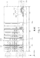
- FIG. 1 is a schematic plan view of a vertical memory device according to an example embodiment of the present disclosure.
- FIG. 1 is illustrated without some components of FIG. 2 , for example, a third interlayer insulating layer 170 is omitted, for ease of description.
- the vertical memory device may include a cell array region CA on which memory cells are formed, a connection region CE in which the memory cells are connected to a wiring, and a peripheral circuit region PC on which peripheral circuits are formed to control the memory cells.
- FIG. 1 illustrates a portion of the cell array region CA.
- the connection region CE may be disposed on one side of the cell array region CA, but the connection region CE may be disposed on opposite sides of the cell array region CA.
- the peripheral circuit region PC may be provided on an exterior of the connection region CE, and a plurality of circuit transistors 210 may be disposed in the peripheral circuit region PC.
- a gate stack GS divided into a plurality of blocks in a y-axis direction by a common source line 180 , may be disposed in the cell array region CA and the connection region CE.
- the gate stack GS may include a plurality of gate electrode layers and a plurality of mold insulating layers alternately stacked on a substrate.
- the common source line 180 may extend from the cell array region CA to the connection region CE.
- the common source line 180 may be electrically connected to the substrate.
- the common source line 180 may include a conductive material.
- the common source lines 180 may include tungsten (W).
- An insulating layer 182 may be disposed between the common source line 180 and the gate stack GS, and the insulating layer 182 may electrically insulate the common source line 180 from the gate electrode layers of the gate stack GS.
- the insulating layers 182 may include silicon oxide (SiO 2 ), silicon nitride (Si 3 N 4 ), silicon oxynitride (SiON) or combinations thereof.
- the cell array region CA may have a plurality of channel structures CHs disposed therein to pass through the gate stack GS, and the connection region CE may have a plurality of dummy channel structures DCHs and a plurality of first and second contact plugs 175 a and 175 b disposed thereon.
- the gate stack GS may, for example, forma first stepped structure extending in an x-axis direction and including a plurality of step layers ST in the connection region CE.
- the first stepped structures may be formed by the gate electrode layers and the mold insulating layers extending from the cell array region CA in the x-axis direction by different lengths.
- Each of the step layers ST may include a first pad region Pa and a second pad region Pb.
- the gate stack GS may include a plurality of first pad regions Pa and a plurality of second pad regions Pb.
- the first pad regions Pa may have the first contact plugs 175 a disposed therein
- the second pad regions Pb may have the second contact plugs 175 b disposed therein.
- the gate stack GS may have a separation insulation pattern 150 disposed in an upper portion thereof, and the separation insulation pattern 150 may divide, into two regions, an uppermost gate electrode layer 131 c of FIG. 2 provided as a string select line.
- the cell array region CA may have the channel structures CHs disposed in a plurality of columns in the x-axis direction.
- FIG. 1 illustrates 8 columns of channel structures CHs between a pair of common source lines 180 as an example.
- the channel structures CHs may be disposed in zigzag form.
- An arrangement of the channel structures CHs is not limited to that illustrated in FIG. 1 , and may be modified in various manners.
- a portion of the channel structures CHs may be formed in a region in which the separation insulation pattern 150 is disposed, and such channel structures CHs may be dummy channel structures that are not connected to a bit line.
- the dummy channel structures DCHs may be disposed adjacent to edges of the respective step layers ST.
- the dummy channel structures DCHs are disposed in four columns in the x-axis direction, as illustrated in FIG. 1 , but an arrangement of the dummy channel structures DCHs is not limited to that illustrated in FIG. 1 .
- a portion of the dummy channel structures DCHs may be disposed adjacent to the edges of the respective step layers ST, and the remainder of the dummy channel structures DCHs may be disposed inside the respective step layers ST.
- the channel structures CHs may have first semiconductor patterns 151 individually disposed therebelow.
- the dummy channel structures DCHs may have second semiconductor patterns 152 individually disposed therebelow.
- FIGS. 2 through 4 are schematic cross-sectional views of a vertical memory device according to an example embodiment of the present disclosure.
- FIG. 2 is a cross-sectional view taken along line I-I′ of FIG. 1
- FIG. 3 is an enlarged view of a region indicated by a dotted line in FIG. 2
- FIG. 4 is a cross-sectional view taken along line II-II′ of FIG. 1 .
- a plurality of gate electrode layers 131 a , 131 b , and 131 c may be stacked on a substrate 101 , and may be spaced apart from each other in a z-axis direction.
- the gate stack GS may extend from the cell array region CA to the connection region CE.
- the cell array region CA may have the channel structures CHs, passing through the gate electrode layers 131 b , and 131 c , and the first semiconductor patterns 151 disposed below the channel structures CHs.
- the connection region CE may have the dummy channel structures DCHs, passing through at least a portion of the gate electrode layer 131 b , and 131 c , and the second semiconductor patterns 152 disposed below the dummy channel structures DCHs.
- the peripheral circuit region PC may have the circuit transistors 210 and a sacrificial layer 121 covering the circuit transistors 210 .
- the sacrificial layer 121 formed in the peripheral circuit region PC, may be an etch stop layer.
- the substrate 101 may have an upper surface extending in the x- and y-axis directions.
- the substrate 101 may include a semiconductor material, such as a group IV semiconductor material, a group III-V compound semiconductor material, or a group II-VI compound semiconductor material.
- a lowermost gate electrode layer 131 a of the gate stack GS may be provided as a ground select line or a lower select line, gate electrode layers 131 b may be provided as word lines, and an uppermost gate electrode layer 131 c may be provided as a string select line or an upper select line.
- the gate electrode layers 131 b may have mold insulating layers 114 disposed therebetween.
- the lowermost gate electrode layer 131 a and the substrate 101 may have a buffer insulating layer 111 disposed therebetween.
- a first interlayer insulating layer 112 and a second interlayer insulating layer 113 may be sequentially disposed between the lowermost gate electrode layer 131 a and a gate electrode layer 131 b adjacent thereto.
- the first interlayer insulating layer 112 may be disposed closer to the substrate 101
- the second interlayer insulating layer 113 may be disposed on the first interlayer insulating layer 112 .
- Each of the circuit transistors 210 may include an active region 207 , a circuit gate dielectric layer 212 , and a circuit gate electrode 214 .
- the circuit gate electrode 214 may have a capping layer 216 formed thereon, and may have a spacer 220 formed on a lateral surface thereof.
- the peripheral circuit region PC may have the sacrificial layer 121 disposed therein to cover the circuit transistor 210 .
- the sacrificial layer 121 and the circuit transistor 210 may have the buffer insulating layer 111 disposed therebetween.
- the first and second interlayer insulating layers 112 and 113 may fully cover the sacrificial layer 121 disposed on the circuit transistor 210 .
- the first and second semiconductor patterns 151 and 152 may extend to the substrate 101 through the lowermost gate electrode layer 131 a , the first interlayer insulating layer 112 , and the buffer insulating layer 111 .
- a first height H 1 of the first semiconductor patterns 151 may be substantially the same as a second height H 2 of the second semiconductor patterns 152 .
- a third height H 3 of the sacrificial layer 121 , covering the circuit transistor 210 may be lower than the first height H 1 of the first semiconductor patterns 151 and the second height H 2 of the second semiconductor patterns 152 .
- upper surfaces of the first semiconductor patterns 151 and upper surfaces of the second semiconductor patterns 152 may be higher than an upper surface of the sacrificial layer 121 .
- the first to third heights H 1 to H 3 may be measured based on an upper surface of the substrate 101 .
- the upper surfaces of the first semiconductor patterns 151 and the upper surfaces of the second semiconductor patterns 152 may be coplanar with an upper surface of the first interlayer insulating layer 112 .
- the number of the lowermost gate electrode layer 131 a , the gate electrode layers 131 b and the uppermost gate electrode layer 131 c forming the gate stack GS is not limited to that of the lowermost gate electrode layer 131 a , the gate electrode layers 131 b , and the uppermost gate electrode layer 131 c illustrated in FIG. 2 .
- the number of gate electrode layers 131 b forming memory cells may be determined, and for example, tens to hundreds of gate electrode layers 131 b may be stacked on the substrate 101 .
- the lowermost gate electrode layer 131 a , the gate electrode layers 131 b , and the uppermost gate electrode layer 131 c may extend from the cell array region CA to the connection region CE in the x-axis direction.
- the lowermost gate electrode layer 131 a , the gate electrode layers 131 b , and the uppermost gate electrode layer 131 c may extend in the connection region CE in the x-axis direction by different lengths to form the first stepped structure.
- each of the step layers ST, forming the first stepped structure may include two gate electrode layers 131 b .
- a lowermost step layer ST of the step layers ST may include a single gate electrode layer 131 a .
- the mold insulating layers 114 may form the first stepped structure along with the gate electrode layers 131 b.
- two respective gate electrode layers 131 b forming the respective step layers ST may have a portion in which the two respective gate electrode layers 131 b do not overlap each other. A portion of an upper gate electrode layer 131 b may be removed from each of the step layers ST.
- a portion of a lower gate electrode layer 131 b not covered by the upper gate electrode layer 131 b may be provided as the first pad region Pa, and the upper gate electrode layer 131 b may be provided as the second pad region Pb spaced apart from the first pad region Pa in the z-axis direction.
- a stepped structure may be formed to have a short length in the y-axis direction within each of the step layers ST forming the first stepped structure.
- the first and second pad regions Pa and Pb may form a second stepped structure in the y-axis direction within each of the step layers ST.
- each of the step layers ST forming the first stepped structure may include three gate electrode layers, and the second stepped structure may include three pad regions provided by the three gate electrode layers. Further, in the connection region CE, a second stepped structure including four or more pad regions may be formed in each of the step layers ST having the first stepped structure.
- the common source line 180 may extend to the substrate 101 , dividing the third interlayer insulating layer 170 , the gate electrode layers 131 b , and the like, in a vertical direction thereof, and may be connected to an impurity region 108 .
- the lowermost gate electrode layer 131 a , the gate electrode layers 131 b , and the uppermost gate electrode layer 131 c may include a conductive material.
- the lowermost gate electrode layer 131 a , the gate electrode layers 131 b , and the uppermost gate electrode layer 131 c may include a metal material, a metal nitride, a metal silicide material, polycrystalline silicon, and combinations thereof.
- the metal material may include, for example, tungsten (W).
- the metal silicide material may include, for example, a silicide material of a metal selected from among, for example, cobalt (Co), nickel (Ni), hafnium (Hf), platinum (Pt), tungsten (W) and titanium (Ti), or may be combinations thereof.
- the metal nitride may include, for example, tungsten nitride (WN), tantalum nitride (TaN), titanium nitride (TiN), or combinations thereof.
- the buffer insulating layer 111 and the mold insulating layers 114 may include silicon oxides.
- the first and second interlayer insulating layers 112 and 113 may include silicon oxides and low-k dielectric materials.
- the first and second semiconductor patterns 151 and 152 may include polycrystalline semiconductor materials.
- the first and second semiconductor patterns 151 and 152 may include, for example, polycrystalline silicon or polycrystalline silicon-germanium.
- the common source line 180 may include, for example, tungsten.
- the channel structures CHs may be disposed in the cell array region CA.
- the channel structures CHs may extend to the first semiconductor patterns 151 through the third interlayer insulating layer 170 , the gate electrode layers 131 b , and the second interlayer insulating layer 113 .
- the dummy channel structures DCHs may extend to the second semiconductor patterns 152 through the third interlayer insulating layer 170 , the gate electrode layers 131 b , and the second interlayer insulating layer 113 .
- the channel structures CHs and the dummy channel structures DCHs may include a gate dielectric layer 161 , a channel layer 163 , a filled insulating layer 165 , and a contact pad 167 , respectively.
- a lower end portion of the channel layer 163 may contact the first or second semiconductor patterns 151 and 152 to be electrically connected thereto, and an upper end portion of the channel layer 163 may contact the contact pad 167 to be electrically connected thereto.
- Ground select gate dielectric layers 155 may be partially disposed between the first semiconductor patterns 151 and the lowermost gate electrode layer 131 a and between the second semiconductor patterns 152 and the lowermost gate electrode layer 131 a .
- the ground select gate dielectric layers 155 may be formed by oxidizing portions of the first and second semiconductor patterns 151 and 152 .
- the second semiconductor patterns 152 may have a greater diameter or width than a diameter or width of the first semiconductor patterns 151 .
- a second diameter D 2 of the second semiconductor patterns 152 may be greater than a first diameter D 1 of the first semiconductor patterns 151 .
- the dummy channel structures DCHs may have a greater diameter or width than a diameter or width of the channel structures CHs.
- a fourth diameter D 4 of the dummy channel structures DCHs may be greater than a third diameter D 3 of the channel structures CHs.
- the gate dielectric layer 161 may surround an outer surface of the channel layer 163 .
- the gate dielectric layer 161 may include a tunneling layer 161 a , a charge storage layer 161 b , and a blocking layer 161 c sequentially disposed from the outer surface of the channel layer 163 .
- the channel layer 163 may have a pipe shape of which a lower end portion is closed. An internal space of the channel layer 163 may be filled by the filled insulating layer 165 .
- the channel layer 163 may include a semiconductor material, such as polycrystalline silicon or monocrystalline silicon.
- the tunneling layer 161 a may include, for example, a silicon oxide.
- a vertical memory device may allow electrons to move to the charge storage layer 161 b through the tunneling layer 161 a in an F-N tunneling manner.
- the charge storage layer 161 b may be a charge trapping layer or a floating gate conductive layer.
- the charge storage layer 161 b may include a dielectric material such as a silicon nitride, quantum dots, or nanocrystals.
- the quantum dots or nanocrystals may include a conductor, for example, microparticles of a metal or a semiconductor material.
- the blocking layer 161 c may include SiO 2 , silicon nitride (Si 3 N 4 ), silicon oxynitride (SiON), or a high-k dielectric material.
- the high-k dielectric material may be any one among aluminum oxide (Al 2 O 3 ), tantalum oxide (Ta 2 O 3 ), titanium oxide (TiO 2 ), yttrium oxide (Y 2 O 3 ), zirconium oxide (ZrO 2 ), zirconium silicon oxide (ZrSi x O y ), hafnium oxide (HfO 2 ), hafnium silicon oxide (HfSi x O y ), lanthanum oxide (La 2 O 3 ), lanthanum aluminum oxide (LaAl x O y ), lanthanum hafnium oxide (LaHf x O y ), hafnium aluminum oxide (HfAl x O y ), and praseodymium oxide (Pr 2 O 3 ).
- FIG. 5 is a schematic cross-sectional view of a vertical memory device according to another example embodiment of the present disclosure.
- a vertical memory device may further include an interface insulating layer 119 disposed between the first and second interlayer insulating layers 112 and 113 , compared with the vertical memory device illustrated in FIG. 2 .
- the interface insulating layer 119 may include, for example, aluminum oxide.
- the remaining components of the vertical memory device, illustrated in FIG. 5 are the same as those of the vertical memory device, illustrated in FIG. 2 , and thus, description thereof will be omitted.
- a structure of the vertical memory device of FIG. 5 may be obtained by further forming the interface insulating layer 119 on a structure, illustrated in FIG. 16 , and then performing processes subsequent to that of FIG. 17 .
- the interface insulating layer 119 may be used as an etch stop layer for an anisotropic etching process of forming channel holes HL 3 and dummy channel holes HL 4 as described with reference to FIG. 19 .
- the interface insulating layer 119 may also prevent the first and second semiconductor patterns 151 and 152 , exposed to lower surfaces of the channel holes HL 3 and the dummy channel holes HL 4 , from being non-uniformly etched by the anisotropic etching process.
- FIGS. 6 and 7 are schematic plan views of vertical memory devices according to other example embodiments of the present disclosure.
- the vertical memory devices may differ from the vertical memory device, illustrated in FIG. 1 , in shapes of second semiconductor patterns 152 a and 152 b .
- the first and second semiconductor patterns 151 and 152 may have cylindrical shapes.
- the first and second semiconductor patterns 151 , 152 a , and 152 b may have different shapes.
- the first semiconductor patterns 151 may have a cylindrical shape
- the second semiconductor patterns 152 a and 152 b may have a bar shape extending in the first direction, for example, the y-axis direction.
- the second semiconductor patterns 152 a may commonly contact two dummy channel structures DCHs disposed adjacent to each other in the first direction, for example, the y-axis direction.
- the second semiconductor patterns 152 b may commonly contact four dummy channel structures DCHs disposed in the first direction, for example, the y-axis direction.
- the second semiconductor patterns 152 b may commonly contact all of the dummy channel structures DCHs disposed in the first direction, for example, the y-axis direction, between a pair of common source lines 180 .
- FIGS. 6 and 7 may be the same as those of the vertical memory device, illustrated in FIG. 1 , and thus, descriptions thereof will be omitted.
- FIGS. 8 and 9 are schematic plan and cross-sectional views of a vertical memory device according to another example embodiment of the present disclosure, respectively.
- the vertical memory device illustrated in FIGS. 8 and 9 , may differ from the vertical memory device, illustrated in FIGS. 1 and 2 , in terms of shapes of second semiconductor patterns 152 a and 152 c.
- the second semiconductor patterns 152 a and 152 c may include first patterns 152 a , having a bar shape extending in the first direction, for example, the y-axis direction, and second patterns 152 c having a bar shape extending in the second direction, for example, the x-axis direction.
- the first patterns 152 a may commonly contact two dummy channel structures DCHs disposed adjacent to each other in the first direction, for example, the y-axis direction
- the second patterns 152 c may commonly contact two dummy channel structures DCHs disposed adjacent to each other in the second direction, for example, the x-axis direction.
- the first patterns 152 a may be disposed at the edge of the stepped structure, formed in the connection region CE, and a disposition of the first patterns 152 a may be modified in various manners.
- FIGS. 10 and 11 are schematic plan and cross-sectional views of a vertical memory device according to another example embodiment of the present disclosure, respectively.
- the vertical memory device illustrated in FIGS. 10 and 11 , may differ from the vertical memory device, illustrated in FIGS. 8 and 9 , in terms of shapes of second semiconductor patterns 152 a and 152 c.
- the second semiconductor patterns 152 a and 152 c may include first patterns 152 a , having a bar shape extending in the first direction, for example, the y-axis direction, and second patterns 152 c having a bar shape extending in the second direction, for example, the x-axis direction.
- the first and second patterns 152 a and 152 c may be alternately disposed in the second direction, for example, the x-axis direction.
- a disposition of the first and second patterns 152 a and 152 c , illustrated in FIGS. 10 and 11 is an example, and may be modified in various manners.
- the first patterns 152 a may commonly contact two dummy channel structures DCHs disposed adjacent to each other in the first direction, for example, the y-axis direction
- the second patterns 152 c may commonly contact two dummy channel structures DCHs disposed adjacent to each other in the second direction, for example, the x-axis direction.
- FIGS. 12, 13, 14, 15, 16, 17, 18, 19, and 20 are cross-sectional views illustrating a method of manufacturing a vertical memory device according to an example embodiment of the present disclosure.
- the method of manufacturing the vertical memory device, illustrated in FIGS. 1 through 4 will hereinafter be described with reference to FIGS. 12 through 20 .
- the substrate 101 may include the cell array region CA, the connection region CE, and the peripheral circuit region PC.
- the circuit transistor 210 forming a peripheral circuit, may be disposed in the peripheral circuit region PC.
- the circuit transistor 210 may include the active region 207 , the circuit gate dielectric layer 212 , and the circuit gate electrode 214 .
- a device separator 205 and the active region 207 defined thereby may be formed in the peripheral circuit region PC.
- the circuit gate dielectric layer 212 and the circuit gate electrode 214 may be disposed in the active region 207 .
- the capping layer 216 may be formed on the circuit gate electrode 214 , and the spacer 220 may be formed on the lateral surface of the circuit gate electrode 214 .
- the buffer insulating layer 111 and the sacrificial layer 121 may be formed on the substrate 101 .
- the buffer insulating layer 111 and the sacrificial layer 121 may be formed in the cell array region CA, the connection region CE, and the peripheral circuit region PC.
- a portion of the buffer insulating layer 111 and a portion of the sacrificial layer 121 between the connection region CE and the peripheral circuit region PC may be removed.
- the buffer insulating layer 111 and the sacrificial layer 121 may be conformally deposited on surfaces of the above structures, formed on the substrate 101 , using a chemical vapor deposition (CVD) process.
- CVD chemical vapor deposition
- the buffer insulating layer 111 and the sacrificial layer 121 , formed in the peripheral circuit region PC, may cover the circuit transistor 210 .
- the buffer insulating layer 111 may include a silicon oxide
- the sacrificial layer 121 may include a silicon nitride.
- the sacrificial layer 121 formed in the cell array region CA and the connection region CE, may be removed by a subsequent gate replacement process.
- the sacrificial layer 121 formed in the peripheral circuit region PC, may remain without being removed.
- the sacrificial layer 121 , formed in the peripheral circuit region PC may be an etch stop layer.
- the first interlayer insulating layer 112 including a first hole HL 1 in the cell array region CA and a second hole HL 2 in the connection region CE, may be formed.
- the first and second holes HL 1 and HL 2 may extend to the substrate 101 through the first interlayer insulating layer 112 , the buffer insulating layer 111 , and the sacrificial layer 121 . Recess regions may be formed in upper portions of the substrate 101 exposed by the first and second holes HL 1 and HL 2 .
- the first and second holes HL 1 and HL 2 may have cylindrical shapes. The first diameter D 1 of the first hole HL 1 may be smaller than the second diameter D 2 of the second hole HL 2 .
- the formation of the first interlayer insulating layer 112 may include forming an insulating layer on the substrate 101 , and then performing a planarization process, for example, a chemical mechanical polishing (CMP) process.
- a height of the first interlayer insulating layer 112 may be adjusted, such that the sacrificial layer 121 disposed in the peripheral circuit region PC may not be exposed.
- the height of the first interlayer insulating layer 112 may be higher than the upper surface of the sacrificial layer 121 covering the circuit transistor 210 disposed in the peripheral circuit region PC.
- the height of the first interlayer insulating layer 112 may be adjusted, such that the sacrificial layer 121 disposed in the peripheral circuit region PC may be exposed.
- the formation of the first and second holes HL 1 and HL 2 may include forming a mask pattern, for example, a photoresist pattern, on the first interlayer insulating layer 112 and continuously and anisotropically etching the first interlayer insulating layer 112 , the sacrificial layer 121 , and the buffer insulating layer 111 until the upper surface of the substrate 101 may be exposed, using the mask pattern as an etching mask. After the completion of the anisotropic etching, the mask pattern may be removed.
- a mask pattern for example, a photoresist pattern
- a semiconductor material layer 115 filling the first and second holes HL 1 and HL 2 , may be formed.
- the semiconductor material layer 115 may fully fill the first and second holes HL 1 and HL 2 using a CVD process.
- the semiconductor material layer 115 may also be formed on the first interlayer insulating layer 112 .
- the semiconductor material layer 115 may include polycrystalline silicon or polycrystalline silicon-germanium.
- the semiconductor material layer 115 may further include impurity ions to be doped.
- the first semiconductor patterns 151 may be formed in the cell array region CA, and the second semiconductor patterns 152 may be formed in the connection region CE.
- the formation of the first and second semiconductor patterns 151 and 152 may include removing the semiconductor material layer 115 that has covered the first interlayer insulating layer 112 using a planarization process, for example, a CMP process.
- the planarization process may cause the upper surface of the first interlayer insulating layer 112 to be exposed.
- the first height H 1 of the first semiconductor patterns 151 may be substantially the same as the second height H 2 of the second semiconductor patterns 152 .
- the first and second heights H 1 and H 2 may be higher than the third height H 3 of the sacrificial layer 121 covering the circuit transistor 210 disposed in the peripheral circuit region PC.
- the first to third heights H 1 to H 3 may be measured based on the upper surface of the substrate 101 .
- the first diameter D 1 of the first semiconductor patterns 151 may be smaller than the second diameter D 2 of the second semiconductor patterns 152 .
- the second interlayer insulating layer 113 and sacrificial layers 122 and the mold insulating layers 114 , alternately stacked on the second interlayer insulating layer 113 , may be formed.
- the sacrificial layers 122 may be formed of a material having etch selectivity with respect to the mold insulating layers 114 .
- the mold insulating layers 114 may include at least one of a silicon oxide layer or a silicon nitride layer
- the sacrificial layers 122 may include at least one of a silicon layer, a silicon oxide layer, a silicon carbide layer or a silicon nitride layer, different from the mold insulating layers 114 .
- the sacrificial layers 122 may include a silicon nitride, and the mold insulating layers 114 may include a silicon oxide.
- the stepped structure may be formed by patterning the mold insulating layers 114 and the sacrificial layers 122 formed in the connection region CE.
- the stepped structure may be formed by patterning the mold insulating layers 114 and the sacrificial layers 122 multiple times.
- Each of the step layers ST, forming the stepped structure may include two mold insulating layers 114 and two sacrificial layers 122 .
- each of the step layers ST may include three or more mold insulating layers 114 and three or more sacrificial layers 122 .
- horizontal lengths of the mold insulating layers 114 and the sacrificial layers 122 may be different from each other.
- the horizontal lengths of the mold insulating layers 114 and the sacrificial layers 122 may be reduced as a distance from the substrate 101 increases.
- the third interlayer insulating layer 170 may be formed on the substrate 101 .
- the third interlayer insulating layer 170 may have a sufficient thickness to cover the cell array region CA and the stepped structure formed in the connection region CE.
- the formation of the third interlayer insulating layer 170 may include a planarization process, for example, a CMP process.
- the channel holes HL 3 may be formed in the cell array region CA, and the dummy channel holes HL 4 may be formed in the connection region CE.
- the formation of the channel holes HL 3 and the dummy channel holes HL 4 may include forming the mask pattern on the third interlayer insulating layer 170 and continuously and anisotropically etching the third interlayer insulating layer 170 , the mold insulating layers 114 , the sacrificial layers 122 , and the second interlayer insulating layer 113 until the upper surfaces of the first and second semiconductor patterns 151 and 152 may be exposed, using the mask pattern as an etching mask.
- the channel holes HL 3 and the dummy channel holes HL 4 may have cylindrical hole shapes.
- the third diameter D 3 of the channel holes HL 3 may be smaller than the fourth diameter D 4 of the dummy channel holes HL 4 .
- the third diameter D 3 of the channel holes HL 3 may be smaller than the first diameter D 1 of the first semiconductor patterns 151
- the fourth diameter D 4 of the dummy channel holes HL 4 may be smaller than the second diameter D 2 of the second semiconductor patterns 152 .
- the third diameter D 3 of the channel holes HL 3 may be the same as the first diameter D 1 of the first semiconductor patterns 151
- the fourth diameter D 4 of the dummy channel holes HL 4 may be the same as the second diameter D 2 of the second semiconductor patterns 152 .
- the channel structures CHs may be formed in the channel holes HL 3 formed on the first semiconductor patterns 151 .
- the dummy channel structures DCHs may be formed in the dummy channel holes HL 4 formed on the second semiconductor patterns 152 .
- Each of the channel structures CHs may include the gate dielectric layer 161 , the channel layer 163 , and the filled insulating layer 165 sequentially stacked in the channel holes HL 3 .
- the channel structures CHs may contact the first semiconductor patterns 151 to be electrically connected to the substrate 101 .
- Lower surfaces of the channel structures CHs may be disposed on a higher level than that of the upper surface of the sacrificial layer 121 covering the circuit transistor 210 disposed in the peripheral circuit region PC.
- the dummy channel structures DCHs may be similar or identical to the channel structures CHs.
- the gate dielectric layers 161 may be formed in the channel holes HL 3 and the dummy channel holes HL 4 to have a pipe shape.
- the gate dielectric layer 161 may include a tunneling layer, a charge storage layer, and a blocking layer sequentially stacked from the channel layer 163 .
- the channel layer 163 may be formed on an interior of the gate dielectric layer 161 .
- the channel layer 163 may have the pipe shape of which the lower end portion is closed.
- the channel layer 163 may include a semiconductor material such as amorphous silicon, polycrystalline silicon or monocrystalline silicon, and the semiconductor material may be a material undoped with an impurity, or a material including a p- or n-type impurity.
- the internal space of the channel layer 163 , defined thereby, may be filled by the filled insulating layer 165 .
- the filled insulating layer 165 may be formed of an insulating material having excellent gap-fill characteristics.
- the channel structures CHs and the dummy channel structures DCHs may further include the contact pad 167 formed on the channel layer 163 and the filled insulating layer 165 , respectively.
- the contact pad 167 may be formed of polycrystalline silicon or a metal material doped with an impurity.
- the gate replacement process may allow the sacrificial layers 121 and 122 to be removed from the cell array region CA and the connection region CE and then fill the sacrificial layers 121 and 122 with conductive materials, thus forming the lowermost gate electrode layer 131 a , the gate electrode layers 131 b , and the uppermost gate electrode layer 131 c .
- trenches, in which the common source lines 180 of FIG. 1 are disposed, may first be formed.
- FIG. 21 is a schematic cross-sectional view of a vertical memory device according to another example embodiment of the present disclosure.
- the vertical memory device illustrated in FIG. 21 , may have a structure in which a cell region CR is disposed on the peripheral circuit region PC.
- the cell region CR may include the cell array region CA and the connection region CE, and may have the same structure as the cell array region CA and the connection region CE. In an example embodiment, the cell region CR may also be disposed below the peripheral circuit region PC.
- the peripheral circuit region PC may include a base substrate 301 , circuit transistors 310 disposed on the base substrate 301 , a buffer insulating layer 311 , and an etch stop layer 321 .
- the base substrate 301 may include an active region 307 defined by a device separator 305 .
- the base substrate 301 may include a semiconductor material, for example, a group IV semiconductor, a group III-V compound semiconductor, or a group II-VI compound semiconductor.
- the group IV semiconductor may include silicon, germanium, or silicon-germanium.
- the base substrate 301 may also be provided as a bulk wafer or an epitaxial layer.
- Each of the circuit transistors 310 may include a circuit gate dielectric layer 312 and a circuit gate electrode 314 .
- a spacer 320 may be formed on a lateral surface of the circuit gate electrode 314 , and a capping layer 316 may be formed on the circuit gate electrode 314 .
- a source/drain region may be disposed on both sides of the circuit gate electrode 314 in the base substrate 301 .
- An interlayer insulating layer 313 may be disposed on the base substrate 301 to cover the circuit transistors 310 .
- Contact plugs and wiring lines, connected to the circuit transistors 310 may be disposed in the peripheral circuit region PC.
- FIG. 22 is a block diagram of an electronic device including a vertical memory device according to an example embodiment of the present disclosure.
- the communication unit 2010 may include a wired/wireless communications module such as a wireless Internet module, a local communications module, a global positioning system (GPS) module, or a mobile communications module.
- the wired/wireless communications module, included in the communications unit 2010 may be connected to an external communications network, based on various communications standards, to transmit and receive data.
- the input unit 2020 may include a mechanical switch, a touchscreen, a voice recognition module, and the like, as a module provided for a user to control operations of the electronic device 2000 .
- the input unit 2020 may also include a mouse or a finger mouse device operating based on a trackball or a laser pointer, and may further include various sensor modules which enable a user to input data.
- the output unit 2030 may output information processed by the electronic device 2000 in audio or video format, and the memory 2040 may store a program for processing or control of the processor 2050 , or data.
- the memory 2040 may include a vertical memory device according to an example embodiment of the present disclosure as described above.
- the processor 2050 may send an instruction to the memory 2040 depending on a required operation to store data in or retrieve data from the memory 2040 .
- the memory 2040 may be embedded in the electronic device 2000 , or may communicate with the processor 2050 through an additional interface. When the memory 2040 communicates with the processor 2050 through the additional interface, the processor 2050 may store data in or retrieve data from the memory 1040 through various interface standards such as secure digital (SD), secure digital high capacity (SDHC), secure digital extended capacity (SDXC), micro SD, universal serial bus (USB), etc.
- SD secure digital
- SDHC secure digital high capacity
- SDXC secure digital extended capacity
- micro SD micro SD
- USB universal serial bus
- the processor 2050 may control operations of each component included in the electronic device 2000 .
- the processor 2050 may perform control and processing associated with a voice call, a video call, data communications, and the like, or may conduct control and processing for multimedia reproduction and management.
- the processor 2050 may also process an input entered by a user through the input unit 2020 and output a result thereof through the output unit 2030 .
- the processor 2050 may store or retrieve data required to control operations of the electronic device 2000 to/from the memory 2040 as described above.
- a vertical memory device having improved reliability may be provided by disposing polycrystalline semiconductor patterns, formed by a planarization process, below channel structures and dummy channel structures.
- circuits may, for example, be embodied in one or more semiconductor chips, or on substrate supports such as printed circuit boards and the like.
- circuits constituting a block may be implemented by dedicated hardware, or by a processor (e.g., one or more programmed microprocessors and associated circuitry), or by a combination of dedicated hardware to perform some functions of the block and a processor to perform other functions of the block.
- a processor e.g., one or more programmed microprocessors and associated circuitry
- Each block of the embodiments may be physically separated into two or more interacting and discrete blocks without departing from the scope of the disclosure.
- the blocks of the embodiments may be physically combined into more complex blocks without departing from the scope of the disclosure.
Abstract
Description
Claims (20)
Applications Claiming Priority (2)
| Application Number | Priority Date | Filing Date | Title |
|---|---|---|---|
| KR1020160145696A KR102650995B1 (en) | 2016-11-03 | 2016-11-03 | Vertical type memory device |
| KR10-2016-0145696 | 2016-11-03 |
Publications (2)
| Publication Number | Publication Date |
|---|---|
| US20180122819A1 US20180122819A1 (en) | 2018-05-03 |
| US10790294B2 true US10790294B2 (en) | 2020-09-29 |
Family
ID=62022517
Family Applications (1)
| Application Number | Title | Priority Date | Filing Date |
|---|---|---|---|
| US15/465,355 Active 2037-09-16 US10790294B2 (en) | 2016-11-03 | 2017-03-21 | Vertical memory device |
Country Status (3)
| Country | Link |
|---|---|
| US (1) | US10790294B2 (en) |
| KR (1) | KR102650995B1 (en) |
| CN (1) | CN108022929B (en) |
Families Citing this family (30)
| Publication number | Priority date | Publication date | Assignee | Title |
|---|---|---|---|---|
| KR20180110797A (en) * | 2017-03-30 | 2018-10-11 | 에스케이하이닉스 주식회사 | Semiconductor device and manufacturing method thereof |
| KR102368932B1 (en) * | 2017-06-01 | 2022-03-02 | 삼성전자주식회사 | Semiconductor Memory Device |
| KR102427324B1 (en) | 2017-07-25 | 2022-07-29 | 삼성전자주식회사 | Three dimensional semiconductor device |
| KR102385566B1 (en) * | 2017-08-30 | 2022-04-12 | 삼성전자주식회사 | Vertical-type memory device |
| KR102641739B1 (en) * | 2018-06-22 | 2024-02-29 | 삼성전자주식회사 | Three-dimensional semiconductor memory devices |
| KR102573272B1 (en) * | 2018-06-22 | 2023-09-01 | 삼성전자주식회사 | Three-dimensional semiconductor memory device |
| JP2020017572A (en) * | 2018-07-23 | 2020-01-30 | キオクシア株式会社 | Semiconductor memory and method of manufacturing the same |
| CN108847413A (en) * | 2018-08-31 | 2018-11-20 | 长江存储科技有限责任公司 | 3D memory device |
| JP2020038911A (en) * | 2018-09-05 | 2020-03-12 | キオクシア株式会社 | Semiconductor memory device and method for manufacturing semiconductor memory device |
| KR20200033370A (en) * | 2018-09-19 | 2020-03-30 | 삼성전자주식회사 | Three-dimensional semiconductor memory devices |
| CN113675206A (en) * | 2018-10-11 | 2021-11-19 | 长江存储科技有限责任公司 | Vertical memory device |
| BR112021007364B1 (en) | 2018-12-07 | 2024-01-30 | Yangtze Memory Technologies Co., Ltd | MEMORY DEVICE |
| KR20200080464A (en) | 2018-12-26 | 2020-07-07 | 삼성전자주식회사 | Three dimensional semiconductor memory device |
| KR20200127715A (en) | 2019-05-03 | 2020-11-11 | 삼성전자주식회사 | Semiconductor devices and manufacturing method for the same |
| CN110289263B (en) * | 2019-06-28 | 2020-04-10 | 长江存储科技有限责任公司 | 3D NAND memory and forming method thereof |
| KR20210016214A (en) | 2019-08-02 | 2021-02-15 | 삼성전자주식회사 | Semiconductor devices |
| US20210098482A1 (en) * | 2019-09-27 | 2021-04-01 | Macronix International Co., Ltd. | Semiconductor structure and manufacturing method thereof |
| US11527549B2 (en) * | 2019-10-04 | 2022-12-13 | SK Hynix Inc. | Memory device and method of manufacturing the same |
| CN113097216B (en) * | 2020-01-16 | 2021-12-21 | 长江存储科技有限责任公司 | Three-dimensional memory and preparation method thereof |
| KR20210097463A (en) * | 2020-01-30 | 2021-08-09 | 에스케이하이닉스 주식회사 | Semiconductor memory device and manufacturing method thereof |
| KR20210128627A (en) * | 2020-04-17 | 2021-10-27 | 에스케이하이닉스 주식회사 | Semiconductor memory device |
| CN112585754A (en) * | 2020-05-27 | 2021-03-30 | 长江存储科技有限责任公司 | Method for forming three-dimensional memory device |
| KR20210158449A (en) * | 2020-06-23 | 2021-12-31 | 삼성전자주식회사 | Semiconductor devices |
| JP2022035130A (en) * | 2020-08-20 | 2022-03-04 | キオクシア株式会社 | Semiconductor storage device |
| CN113039643A (en) * | 2020-09-02 | 2021-06-25 | 长江存储科技有限责任公司 | On-chip capacitor in semiconductor device and method of forming the same |
| KR20220040846A (en) * | 2020-09-24 | 2022-03-31 | 삼성전자주식회사 | Integrated circuit device and electronic system having the same |
| CN112543996A (en) * | 2020-11-06 | 2021-03-23 | 长江存储科技有限责任公司 | Three-dimensional NAND memory device with novel dummy channel structure |
| JP2022094651A (en) * | 2020-12-15 | 2022-06-27 | キオクシア株式会社 | Semiconductor device and method for manufacturing semiconductor device |
| CN112838094A (en) * | 2021-01-04 | 2021-05-25 | 长江存储科技有限责任公司 | Three-dimensional memory device |
| CN113161367B (en) * | 2021-03-04 | 2022-08-19 | 长江存储科技有限责任公司 | Semiconductor structure and manufacturing method thereof |
Citations (20)
| Publication number | Priority date | Publication date | Assignee | Title |
|---|---|---|---|---|
| US7847334B2 (en) | 2008-03-14 | 2010-12-07 | Kabushiki Kaisha Toshiba | Non-volatile semiconductor storage device and method of manufacturing the same |
| US8013389B2 (en) | 2008-11-06 | 2011-09-06 | Samsung Electronics Co., Ltd. | Three-dimensional nonvolatile memory devices having sub-divided active bars and methods of manufacturing such devices |
| KR101082098B1 (en) | 2008-09-24 | 2011-11-10 | 주식회사 하이닉스반도체 | Method for fabricating flash memory device having 3-dimensional structure |
| US8193571B2 (en) | 2008-08-18 | 2012-06-05 | Kabushiki Kaisha Toshiba | Stacked type nonvolatile semiconductor memory device and method of manufacturing same |
| US8237211B2 (en) | 2008-10-20 | 2012-08-07 | Kabushiki Kaisha Toshiba | Non-volatile semiconductor storage device and method of manufacturing the same |
| US8343820B2 (en) | 2009-09-07 | 2013-01-01 | Hynix Semiconductor Inc. | Method for fabricating vertical channel type non-volatile memory device |
| US20140048873A1 (en) | 2010-09-27 | 2014-02-20 | Samsung Electronics Co., Ltd. | Semiconductor devices |
| US8941154B2 (en) | 2010-12-30 | 2015-01-27 | SK Hynix Inc. | Non-volatile memory device and method for fabricating the same |
| US9076865B2 (en) | 2012-08-24 | 2015-07-07 | SK Hynix Inc. | Non-volatile memory device, method of operating the same and method of fabricating the same |
| US20150340376A1 (en) * | 2014-05-20 | 2015-11-26 | Jintaek Park | Semiconductor device and method of fabricating the same |
| KR101579587B1 (en) | 2009-04-01 | 2015-12-22 | 삼성전자주식회사 | Semiconductor device and method of forming the same |
| US9224747B2 (en) | 2014-03-26 | 2015-12-29 | Sandisk Technologies Inc. | Vertical NAND device with shared word line steps |
| US20160027796A1 (en) * | 2014-07-28 | 2016-01-28 | Hyung-Mo Yang | Semiconductor devices |
| US9305934B1 (en) | 2014-10-17 | 2016-04-05 | Sandisk Technologies Inc. | Vertical NAND device containing peripheral devices on epitaxial semiconductor pedestal |
| US9337237B2 (en) | 2009-11-02 | 2016-05-10 | Micron Technology, Inc. | Methods, structures and devices for increasing memory density |
| US20160225785A1 (en) * | 2015-01-30 | 2016-08-04 | Chaeho Kim | Semiconductor memory device and method of fabricating the same |
| US20160351497A1 (en) * | 2015-02-04 | 2016-12-01 | Sandisk Technologies Llc | Cobalt-containing conductive layers for control gate electrodes in a memory structure |
| US20170040337A1 (en) * | 2015-08-07 | 2017-02-09 | Jong Won Kim | Vertical memory devices having dummy channel regions |
| US20170062454A1 (en) * | 2015-08-25 | 2017-03-02 | Sandisk Technologies Inc. | Method of making a multilevel memory stack structure using a cavity containing a sacrificial fill material |
| US20180130812A1 (en) * | 2016-11-09 | 2018-05-10 | Sandisk Technologies Llc | Three-dimensional memory device with electrically isolated support pillar structures and method of making thereof |
Family Cites Families (5)
| Publication number | Priority date | Publication date | Assignee | Title |
|---|---|---|---|---|
| KR101585616B1 (en) * | 2009-12-16 | 2016-01-15 | 삼성전자주식회사 | Semiconductor device and method for fabricating the same |
| KR20140018541A (en) * | 2012-08-02 | 2014-02-13 | 에스케이하이닉스 주식회사 | Nonvolatile memory device and method for fabricating the same |
| US9041090B2 (en) * | 2013-05-15 | 2015-05-26 | Micron Technology, Inc. | Methods for forming a string of memory cells and apparatuses having a vertical string of memory cells including metal |
| KR102341716B1 (en) * | 2015-01-30 | 2021-12-27 | 삼성전자주식회사 | Semiconductor memory device and method of fabricating the same |
| US9780182B2 (en) | 2015-02-04 | 2017-10-03 | Sandisk Technologies Llc | Molybdenum-containing conductive layers for control gate electrodes in a memory structure |
-
2016
- 2016-11-03 KR KR1020160145696A patent/KR102650995B1/en active IP Right Grant
-
2017
- 2017-03-21 US US15/465,355 patent/US10790294B2/en active Active
- 2017-11-02 CN CN201711064262.4A patent/CN108022929B/en active Active
Patent Citations (20)
| Publication number | Priority date | Publication date | Assignee | Title |
|---|---|---|---|---|
| US7847334B2 (en) | 2008-03-14 | 2010-12-07 | Kabushiki Kaisha Toshiba | Non-volatile semiconductor storage device and method of manufacturing the same |
| US8193571B2 (en) | 2008-08-18 | 2012-06-05 | Kabushiki Kaisha Toshiba | Stacked type nonvolatile semiconductor memory device and method of manufacturing same |
| KR101082098B1 (en) | 2008-09-24 | 2011-11-10 | 주식회사 하이닉스반도체 | Method for fabricating flash memory device having 3-dimensional structure |
| US8237211B2 (en) | 2008-10-20 | 2012-08-07 | Kabushiki Kaisha Toshiba | Non-volatile semiconductor storage device and method of manufacturing the same |
| US8013389B2 (en) | 2008-11-06 | 2011-09-06 | Samsung Electronics Co., Ltd. | Three-dimensional nonvolatile memory devices having sub-divided active bars and methods of manufacturing such devices |
| KR101579587B1 (en) | 2009-04-01 | 2015-12-22 | 삼성전자주식회사 | Semiconductor device and method of forming the same |
| US8343820B2 (en) | 2009-09-07 | 2013-01-01 | Hynix Semiconductor Inc. | Method for fabricating vertical channel type non-volatile memory device |
| US9337237B2 (en) | 2009-11-02 | 2016-05-10 | Micron Technology, Inc. | Methods, structures and devices for increasing memory density |
| US20140048873A1 (en) | 2010-09-27 | 2014-02-20 | Samsung Electronics Co., Ltd. | Semiconductor devices |
| US8941154B2 (en) | 2010-12-30 | 2015-01-27 | SK Hynix Inc. | Non-volatile memory device and method for fabricating the same |
| US9076865B2 (en) | 2012-08-24 | 2015-07-07 | SK Hynix Inc. | Non-volatile memory device, method of operating the same and method of fabricating the same |
| US9224747B2 (en) | 2014-03-26 | 2015-12-29 | Sandisk Technologies Inc. | Vertical NAND device with shared word line steps |
| US20150340376A1 (en) * | 2014-05-20 | 2015-11-26 | Jintaek Park | Semiconductor device and method of fabricating the same |
| US20160027796A1 (en) * | 2014-07-28 | 2016-01-28 | Hyung-Mo Yang | Semiconductor devices |
| US9305934B1 (en) | 2014-10-17 | 2016-04-05 | Sandisk Technologies Inc. | Vertical NAND device containing peripheral devices on epitaxial semiconductor pedestal |
| US20160225785A1 (en) * | 2015-01-30 | 2016-08-04 | Chaeho Kim | Semiconductor memory device and method of fabricating the same |
| US20160351497A1 (en) * | 2015-02-04 | 2016-12-01 | Sandisk Technologies Llc | Cobalt-containing conductive layers for control gate electrodes in a memory structure |
| US20170040337A1 (en) * | 2015-08-07 | 2017-02-09 | Jong Won Kim | Vertical memory devices having dummy channel regions |
| US20170062454A1 (en) * | 2015-08-25 | 2017-03-02 | Sandisk Technologies Inc. | Method of making a multilevel memory stack structure using a cavity containing a sacrificial fill material |
| US20180130812A1 (en) * | 2016-11-09 | 2018-05-10 | Sandisk Technologies Llc | Three-dimensional memory device with electrically isolated support pillar structures and method of making thereof |
Also Published As
| Publication number | Publication date |
|---|---|
| CN108022929A (en) | 2018-05-11 |
| CN108022929B (en) | 2023-07-04 |
| KR102650995B1 (en) | 2024-03-25 |
| US20180122819A1 (en) | 2018-05-03 |
| KR20180049593A (en) | 2018-05-11 |
Similar Documents
| Publication | Publication Date | Title |
|---|---|---|
| US10790294B2 (en) | Vertical memory device | |
| US9899411B2 (en) | Three-dimensional semiconductor memory device and method for fabricating the same | |
| EP3420595B1 (en) | Within-array through-memory-level via structures | |
| US10644020B2 (en) | Three-dimensional semiconductor memory device with a substrate contact region and method of manufacturing the same | |
| US9576902B2 (en) | Semiconductor device including landing pad | |
| US9905568B2 (en) | Nonvolatile memory device and a method for fabricating the same | |
| US8748249B2 (en) | Vertical structure non-volatile memory device and method of manufacturing the same | |
| CN111244091B (en) | Method for manufacturing semiconductor device | |
| US10121906B2 (en) | Vertical memory strings, and vertically-stacked structures | |
| US9431416B2 (en) | Vertical-type nonvolatile memory device and method of manufacturing the same | |
| US8685821B2 (en) | Vertical channel memory devices with nonuniform gate electrodes and methods of fabricating the same | |
| US8822322B2 (en) | Semiconductor devices and methods of fabricating the same | |
| US8987860B2 (en) | Semiconductor device | |
| EP2259306A1 (en) | Semiconductor memory and method for manufacturing the same | |
| US10886167B2 (en) | Semiconductor device for improving device characteristics | |
| US10847630B2 (en) | Semiconductor device and method of manufacturing the same | |
| US20210066343A1 (en) | Integrated circuit device and method of manufacturing the same | |
| CN108155173B (en) | Semiconductor device including bit line | |
| US9362289B2 (en) | Semiconductor device including landing pad | |
| US8445343B2 (en) | Methods of fabricating semiconductor devices including semiconductor layers formed in stacked insulating layers | |
| CN115206981A (en) | Integrated circuit system, memory array and method for forming memory array | |
| US9754944B2 (en) | Method of manufacturing semiconductor device |
Legal Events
| Date | Code | Title | Description |
|---|---|---|---|
| AS | Assignment |
Owner name: SAMSUNG ELECTRONICS CO., LTD., KOREA, REPUBLIC OF Free format text: ASSIGNMENT OF ASSIGNORS INTEREST;ASSIGNORS:SHIM, JAE JOO;CHO, SEONG SOON;KIM, JI HYE;AND OTHERS;SIGNING DATES FROM 20170307 TO 20170317;REEL/FRAME:041671/0096 |
|
| STPP | Information on status: patent application and granting procedure in general |
Free format text: RESPONSE TO NON-FINAL OFFICE ACTION ENTERED AND FORWARDED TO EXAMINER |
|
| STPP | Information on status: patent application and granting procedure in general |
Free format text: FINAL REJECTION MAILED |
|
| STPP | Information on status: patent application and granting procedure in general |
Free format text: ADVISORY ACTION MAILED |
|
| STPP | Information on status: patent application and granting procedure in general |
Free format text: DOCKETED NEW CASE - READY FOR EXAMINATION |
|
| STPP | Information on status: patent application and granting procedure in general |
Free format text: NON FINAL ACTION MAILED |
|
| STPP | Information on status: patent application and granting procedure in general |
Free format text: NOTICE OF ALLOWANCE MAILED -- APPLICATION RECEIVED IN OFFICE OF PUBLICATIONS |
|
| STCF | Information on status: patent grant |
Free format text: PATENTED CASE |
|
| MAFP | Maintenance fee payment |
Free format text: PAYMENT OF MAINTENANCE FEE, 4TH YEAR, LARGE ENTITY (ORIGINAL EVENT CODE: M1551); ENTITY STATUS OF PATENT OWNER: LARGE ENTITY Year of fee payment: 4 |