US10771048B2 - Measurement of the duration of a pulse - Google Patents
Measurement of the duration of a pulse Download PDFInfo
- Publication number
- US10771048B2 US10771048B2 US16/747,341 US202016747341A US10771048B2 US 10771048 B2 US10771048 B2 US 10771048B2 US 202016747341 A US202016747341 A US 202016747341A US 10771048 B2 US10771048 B2 US 10771048B2
- Authority
- US
- United States
- Prior art keywords
- circuit
- input
- output
- pulse
- signal
- Prior art date
- Legal status (The legal status is an assumption and is not a legal conclusion. Google has not performed a legal analysis and makes no representation as to the accuracy of the status listed.)
- Active
Links
Images


Classifications
-
- G—PHYSICS
- G01—MEASURING; TESTING
- G01R—MEASURING ELECTRIC VARIABLES; MEASURING MAGNETIC VARIABLES
- G01R29/00—Arrangements for measuring or indicating electric quantities not covered by groups G01R19/00 - G01R27/00
- G01R29/02—Measuring characteristics of individual pulses, e.g. deviation from pulse flatness, rise time or duration
- G01R29/023—Measuring pulse width
-
- H—ELECTRICITY
- H03—ELECTRONIC CIRCUITRY
- H03K—PULSE TECHNIQUE
- H03K5/00—Manipulating of pulses not covered by one of the other main groups of this subclass
- H03K5/13—Arrangements having a single output and transforming input signals into pulses delivered at desired time intervals
- H03K5/14—Arrangements having a single output and transforming input signals into pulses delivered at desired time intervals by the use of delay lines
-
- H—ELECTRICITY
- H03—ELECTRONIC CIRCUITRY
- H03K—PULSE TECHNIQUE
- H03K5/00—Manipulating of pulses not covered by one of the other main groups of this subclass
- H03K5/13—Arrangements having a single output and transforming input signals into pulses delivered at desired time intervals
- H03K5/135—Arrangements having a single output and transforming input signals into pulses delivered at desired time intervals by the use of time reference signals, e.g. clock signals
-
- G—PHYSICS
- G01—MEASURING; TESTING
- G01R—MEASURING ELECTRIC VARIABLES; MEASURING MAGNETIC VARIABLES
- G01R35/00—Testing or calibrating of apparatus covered by the other groups of this subclass
- G01R35/005—Calibrating; Standards or reference devices, e.g. voltage or resistance standards, "golden" references
-
- H—ELECTRICITY
- H03—ELECTRONIC CIRCUITRY
- H03K—PULSE TECHNIQUE
- H03K5/00—Manipulating of pulses not covered by one of the other main groups of this subclass
- H03K2005/00013—Delay, i.e. output pulse is delayed after input pulse and pulse length of output pulse is dependent on pulse length of input pulse
- H03K2005/0015—Layout of the delay element
- H03K2005/00163—Layout of the delay element using bipolar transistors
- H03K2005/00176—Layout of the delay element using bipolar transistors using differential stages
-
- H—ELECTRICITY
- H03—ELECTRONIC CIRCUITRY
- H03K—PULSE TECHNIQUE
- H03K5/00—Manipulating of pulses not covered by one of the other main groups of this subclass
- H03K2005/00013—Delay, i.e. output pulse is delayed after input pulse and pulse length of output pulse is dependent on pulse length of input pulse
- H03K2005/0015—Layout of the delay element
- H03K2005/00234—Layout of the delay element using circuits having two logic levels
- H03K2005/00273—Layout of the delay element using circuits having two logic levels using digital comparators
Definitions
- the present disclosure generally concerns electronic circuits and, in particular, electronic circuits for measuring the duration of a pulse, particularly circuits of detection and characterization of a radiating particle based on the voltage pulse generated by the particle when it hits a combinational logic circuit.
- Circuits are known in the art for detection and characterization of a radiating particle comprising at least a first combinational logic circuit configured to propagate a pulse generated in the combinational logic circuit when it is hit by a radiating particle, and a second circuit configured to supply a signal representative of the duration of the generated pulse to characterize the particle.
- a transient voltage pulse generally designated with acronym SET (“Single Event Transient”)
- the duration of the pulse is representative of characteristics of the particle, for example, of its type and/or of its power.
- an error with respect to the measurement of the duration of the pulse may result in an erroneous characterization of the particle.
- An embodiment overcomes all or part of the disadvantages of known circuits for measuring the duration of a voltage pulse, in particular of known circuits of detection and of characterization of a radiating particle.
- An embodiment provides a circuit or device for measuring the duration of a voltage pulse enabling to correct measurement errors, particularly due to manufacturing variations.
- An embodiment more particularly provides a device for measuring the duration of a voltage pulse delivering output signals from which the error on the measurement of the duration of the pulse is estimated.
- an embodiment provides a device comprising: a first circuit comprising a first chain of identical stages defining first and second delay lines; a second circuit comprising a second chain of stages identical to the stages of the first chain, the second chain defining third and fourth delay lines; and a third circuit selectively coupling the third delay line, the fourth delay line, or a first input of the third circuit to a same input of the first circuit.
- the number of stages of the second circuit is smaller than the number of stages of the first circuit.
- the first circuit preferably a vernier delay line circuit, is configured to deliver an output signal representative of a duration of a pulse received by said same first input of the first circuit.
- the device further comprises: a fourth circuit connected to the third delay line and configured to deliver to the third circuit a first pulse having a duration representative of the delay introduced by the third delay line; and a fifth circuit connected to the fourth delay line and configured to deliver to the third circuit a second pulse having a duration representative of the delay introduced by the fourth delay line, the third circuit being configured to selectively deliver, to said same input of the first circuit, the first pulse, the second pulse, or a pulse received by the first input of the third circuit, according to a control signal received by a second input of the third circuit.
- each stage in the first chain introduces a first delay on the first delay line and a second delay on the second delay line
- each stage in the second chain introduces the first delay on the third delay line and the second delay on the fourth delay line, the second delay being longer than the first delay
- each stage comprises a synchronous flip-flop; a fourth circuit coupling a first input of the stage to a first output of the stage and to a data input of the synchronous flip-flop, the fourth circuit being configured to propagate a signal with the first delay; and a fifth circuit coupling a second input of the stage to a second output of the stage and to a synchronization input of the synchronous flip-flop, the fifth circuit being configured to propagate a signal with the second delay.
- the device further comprises a sixth circuit having an output connected to the first input of the third circuit and having an input intended to receive a pulse, the sixth circuit being configured to deliver at its output a pulse longer by a given duration than the pulse received by its input.
- the device further comprises a seventh circuit configured to selectively deliver, at the input of the sixth circuit, one of the first and second pulses or a pulse received on a first input of the seventh circuit, according to a control signal received by a second input of the seventh circuit.
- the device further comprises at least one eighth circuit configured to propagate a pulse to an output of the eighth circuit, the output of the eighth circuit being coupled to the first input of the seventh circuit.
- the device further comprises a ninth circuit having an output coupled to an input of said at least one eighth circuit, the ninth circuit being configured to deliver at its output a same pulse each time an input of the eighth circuit receives a corresponding control signal.
- the device comprises at least two eighth circuits.
- the device comprises a tenth circuit configured to selectively couple, according to a control signal received by an input of the tenth circuit, the output of the ninth circuit to the input of one of the eighth circuits; and an eleventh circuit configured to deliver to the first input of the seventh circuit a signal corresponding to the logic OR of the outputs of the eighth circuits.
- the device comprises a tenth circuit configured to selectively couple, according to a control signal received by an input of the tenth circuit, the outputs of the eighth circuits to corresponding outputs of the tenth circuit or the output of a single one of the eighth circuits to the output of the tenth circuit corresponding to said single one of the eighth circuits; and an eleventh circuit configured to deliver, to the first input of the seventh circuit, a signal corresponding to the logic OR of the outputs of the tenth circuit.
- the device further comprises a twelfth circuit configured to deliver a signal indicating which of the eighth circuits a pulse received by the first input of the seventh circuit originates from.
- the device further comprises a control circuit configured to deliver an input signal to the third delay line and to the fourth delay line.
- control circuit is further configured to deliver the control signal of the third circuit and/or the control signal of the seventh circuit and/or the control signal of the ninth circuit and/or the control signal of the tenth circuit.
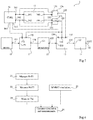
- FIG. 1 schematically shows in the form of blocks an embodiment of a device configured to detect and characterize a radiating particle
- FIG. 2 shows in the form of blocks steps of an embodiment of a method of calibrating the device of FIG. 1 ;
- FIG. 3 shows an embodiment of a circuit of the device of FIG. 1 , in more detailed fashion than in FIG. 1 ;
- FIGS. 4A, 4B, and 4C show embodiments of another circuit of the device of FIG. 1 , in more detailed fashion than in FIG. 1 ;
- FIG. 5 schematically shows in the form of blocks of alternative embodiment of the device of FIG. 1 ;
- FIG. 6 shows in the form of blocks steps of an embodiment of a method of calibrating the device of FIG. 5 ;
- FIG. 7 schematically shows in the form of blocks another alternative embodiment of the device of FIG. 1 ;
- FIG. 8 shows in the form of blocks steps of an embodiment of a method of calibrating the device of FIG. 7 ;
- FIG. 9 schematically shows in the form of blocks still another alternative embodiment of the device of FIG. 1 .
- connection is used to designate a direct electrical connection between circuit elements with no intermediate elements other than conductors
- coupled is used to designate an electrical connection between circuit elements that may be direct, or may be via one or more intermediate elements.
- a signal which alternates between a first constant state, for example, a low state, noted “0”, and a second constant state, for example, a high state, noted “1”, is called “binary signal”.
- the states “1” and “0” of a binary signal correspond to the respective values “1” and “0” of a bit represented by the binary signal.
- the high and low states of different binary signals of a same electronic circuit may be different.
- the binary signals may correspond to voltages which may not be perfectly constant in the high or low state.
- FIG. 1 schematically shows in the form of blocks an embodiment of a circuit or device 1 configured to detect and characterize a radiating particle.
- Device 1 preferably an integrated circuit, comprises at least one circuit or sensor 10 (SENSOR), a single sensor 10 in the example of FIG. 1 .
- Circuit 10 is a combinational logic circuit configured so that, when a radiating particle hits circuit 10 and generates a transient voltage pulse therein, circuit 10 propagates the pulse, without deforming it, to an output 101 of circuit 10 .
- Device 1 further comprises a circuit 11 .
- Circuit 11 here a vernier delay line or VDL, is configured to deliver, at the level of an output 111 of circuit 11 , a digital signal or binary word OUT representative of the duration of a pulse received by an input 112 of circuit 11 .
- Input 112 of circuit 11 is coupled to output 101 of circuit 10 , in this embodiment via two circuits 12 and 13 .
- Circuit 11 comprises a chain of identical stages or elementary circuits 113 a , for example, a chain of 256 stages 113 a .
- the chain of stages 113 a is connected between input 112 and output 111 of circuit 11 .
- Each stage 113 a comprises two inputs 1131 and 1132 , two outputs 1133 and 1134 , two circuits 1135 and 1136 , and one synchronous flip-flop 1137 .
- the inputs 1131 and 1132 of first stage 113 a of the chain (on the left-hand side in FIG. 1 ) are connected to a same input 112 of circuit 11 .
- the outputs 1133 and 1134 of each stage 113 a of the chain except for those of the last stage 113 a (on the right-hand side in FIG.
- outputs 1133 and 1134 of the last stage 113 a in the chain are not connected or, in other words, are omitted.
- circuit 1135 is connected between the input 1131 and the output 1133 of the considered stage.
- the output of circuit 1135 of stage 113 a is further connected to an input, here the data input D, of flip-flop 1137 of the stage.
- the output of circuit 1135 of stage 113 a forms output 1133 of the stage.
- Circuit 1135 is configured to introduce a first delay T 1 between input 1131 and output 1133 of the stage, and thus the D input of flip-flop 1137 .
- each circuit 1135 is formed of two inverters series-connected between the input and the output of circuit 1135 or, in other words, between input 1131 and output 1133 of the considered stage.
- circuit 1136 is connected between input 1132 and output 1134 of the considered stage.
- Output 1134 of the stage that is, the output of circuit 1136 of this stage, is connected to an input, here, the synchronization input C, of flip-flop 1137 of the stage.
- Circuit 1136 is configured to introduce a second delay T 2 , longer than delay T 1 , between input 1132 and output 1134 of the stage, and thus input C of flip-flop 1137 .
- each circuit 1136 is formed of two inverters series-connected between the input and the output of circuit 1136 or, in other words, between input 1132 and output 1134 of the considered stage.
- Each flip-flop 1137 comprises an output O delivering a binary signal.
- the assembly of the binary signals supplied by the O outputs of the flip-flops 1137 of circuit 11 or, in other words, the concatenation of the output bits of flip-flops 1137 forms a digital signal, or binary word, representative of the duration of the pulse received by input 112 of circuit 11 .
- each flip-flop 1137 is configured to store, on each rising edge of the binary signal present on its C input, the high or low state of the binary signal present on its D input, and to maintain the binary signal supplied by its O output at the stored state until the next rising edge on its C input.
- signal OUT corresponds to the concatenation of the output signals of flip-flops 1137 of circuit 11 .
- circuit 11 comprises a circuit supplying signal OUT from all the output signals of flip-flops 1137 , so that signal OUT corresponds to a binary word comprising less bits than there are stages 113 a in circuits 11 .
- Circuit 12 (BROADENING) comprises an input 121 and an output 122 .
- Input 121 is coupled, here connected, to output 101 of circuit 10 .
- circuit 12 When it receives a pulse of duration Tpulse on its input 121 , circuit 12 is configured to supply, on its output 122 , a pulse of duration Tbd+Tpulse, Tbd being a constant duration.
- circuit 12 is configured to lengthen by a duration Tbd the duration Tpulse of a pulse that it receives.
- circuit 12 may be omitted. However, omitting circuit 12 generates the risk that, when a transient voltage pulse is generated by a particle reaching circuit 10 , the duration thereof is too short to be detected by circuit 11 .
- Device 1 further comprises a circuit 14 comprising a chain of stages 113 b identical to the stages 113 a of the chain of circuit 11 .
- Circuit 14 comprises inputs 141 and 142 connected to the respective inputs 1131 and 1132 of the first stage 113 b (on the left-hand side in FIG. 1 ).
- Outputs 1133 and 1134 of the last stage 113 b are connected to respective outputs 143 and 144 of circuit 14 .
- the number N of stages 113 b of the chain of circuit 14 is smaller than the number of stages 113 a of the chain of circuit 11 .
- Stages 113 b are connected one after the others in the same way as stages 113 a .
- the series connection of circuits 1135 of circuit 14 forms a first delay line of circuit 14
- the series connection of circuits 1136 of circuit 14 forms a second delay line of circuit 14 , parallel to the first delay line of circuit 14 .
- the outputs O of flip-flops 1137 of stages 113 b are not connected or, in other words, are not used to deliver an output signal of circuit 14 .
- Device 1 comprises two circuits 15 a and 15 b , preferably identical to each other.
- Circuit 15 a , respectively 15 b comprises an input 151 connected to input 141 , respectively 142 , of circuit 14 , and an input 152 connected to output 143 , respectively 144 , of circuit 14 .
- circuit 15 a is connected to the end of the first delay line of circuit 14
- circuit 15 b being connected to the ends of the second delay line of circuit 14 .
- Each circuit 15 a , 15 b comprises an output 153 .
- Each circuit 15 a , 15 b is configured to deliver a pulse having a duration corresponding to the delay introduced by the delay line of the circuit 14 to which it is connected.
- each circuit 15 a , 15 b is configured to deliver a binary output signal in the high state only if the signals received by its inputs 151 and 152 are respectively in the high state and in the low state.
- each circuit 15 a , 15 b comprises a NOR gate having a first input receiving the inverse or the complement (inverter 154 ) of the signal received by the input 151 of circuit 15 a , respectively 15 b , having a second input receiving the signal received by the input 152 of circuit 15 a , respectively 15 b , and having its output delivering the output signal of circuit 15 a , respectively 15 b .
- NOR gate technology for the circuits 15 a , 15 b is just by example and that suitable logic circuit configuration could be used.
- Circuit 13 of device 1 comprises three inputs 131 , 132 , and 133 respectively connected to output 153 of circuit 15 a , to output 153 of circuit 15 b , and to output 122 of circuit 12 .
- Circuit 13 also comprises an input 134 receiving a control signal, and an output 135 .
- Circuit 13 is configured to selectively couple, according to the control signal that it receives, one of inputs 131 , 132 , and 133 to output 135 .
- the first delay line of circuit 14 (assembly of circuits 1135 of circuit 14 ) and the second delay line of circuit 14 (assembly of circuits 1136 of circuit 14 ) are selectively coupled to input 112 of circuit 11 by circuit 13 .
- Device 1 also comprises a control circuit 16 (CTRL).
- Circuit 16 comprises three outputs 161 , 162 , and 163 connected to the respective inputs 141 , 142 , and 134 of circuits 14 and 13 .
- Circuit 16 is configured to deliver a binary signal either to input 141 , or to input 142 , which signal may possibly be identical and simultaneously sent to the two inputs 141 and 142 .
- Circuit 16 is further configured to deliver the control signal to input 134 of circuit 13 .
- inputs 141 and 142 of circuit 14 are merged together, the outputs 161 and 162 of circuit 16 also being merged together.
- outputs 153 of circuits 15 a and 15 b are coupled to a single input of circuit 13 , via an OR logic function, for example, by an OR gate.
- circuit 16 is configured to deliver a signal to a first one of the two inputs 141 and 142 , and then to the second one of the two inputs.
- circuit 16 controls circuit 13 so that input 133 is coupled to output 135 .
- a particle hits circuit 10 and generates a voltage pulse therein, that is, here, a short passage in the high state of a binary signal normally in the low state
- the pulse is transmitted to circuit 12 , which lengthens by duration Tbd the duration Tpulse of the pulse.
- the pulse of lengthened duration is then supplied to input 112 of circuit 11 , via circuit 13 .
- a first corresponding pulse then propagates in the first delay line of circuit 11 (assembly of the circuits 1135 of circuit 11 ), a second corresponding pulse propagating in the second delay line of circuit 11 (assembly of the circuits 1136 of circuit 11 ).
- the first and second pulses have the same duration, here, Tpulse+Tbd, as the pulse received by circuit 11 . Due to the fact that delay T 1 is shorter than delay T 2 , at each stage 113 a crossed by the first and second pulses, the second pulse is delayed by a duration T 2 ⁇ T 1 with respect to the first pulse. For a given stage 113 a , if the delay between the first and second pulses is such that the rising edge of the second pulse occurs while the first pulse is in the high state, the O output of flip-flop 1137 of this stage 113 a is in the high state, that is, at “1”.
- the O output of the flip-flop 1137 of this stage 113 a is in the low state, that is, “0”.
- the number A of stages 113 a having their flip-flop 1137 supplying an output at “1” is representative of the duration Tpulse+Tbd of the pulse, which duration is in the range from A*(T 2 ⁇ T 1 ) to (A+1)*(T 2 ⁇ T 1 ). Knowing the values of delays T 1 and T 2 and of duration Tbd, a range of values comprising duration Tpulse of the pulse generated in circuit 10 can thus be determined.
- the real or practical values of delays T 1 and T 2 may be different from the known theoretical or design values of delays T 1 and T 2 , particularly due to manufacturing dispersions of device 1 .
- Device 1 enables to estimate, for each of delays T 1 and T 2 , the practical or real value of the delay. Thereby, the duration of the pulse received by circuit 11 may be estimated with a greater accuracy than if only the theoretical values of delays T 1 and T 2 were used.
- FIG. 2 shows, in the form of blocks, steps of an embodiment of a method of calibration of the device of FIG. 1 . More particularly, the method enables to estimate, after the manufacturing of device 1 , the practical values of each of delays T 1 and T 2 of device 1 .
- circuit 16 controls circuit 13 so that it couples its input 131 to its output 134 . Circuit 16 then switches, from the low state to the high state, the binary signal delivered to input 141 of circuit 14 . As a result, output 153 of circuit 15 a delivers a pulse of duration N*T 1 (N being the number of stages 113 b ) which is transmitted, via circuit 13 , to input 112 of circuit 11 . Circuit 11 then delivers a digital signal or binary word OUT representative of duration N*T 1 of the received pulse. At the end of step 21 , circuit 16 switches, from the high state to the low state, the signal delivered to input 141 of circuit 14 .
- step 22 (block “Measure N*T 2 ”), the order of steps 21 and 22 being capable of being inverted, circuit 16 control circuit 13 so that the latter couples its input 132 to its output 134 .
- Circuit 16 then switches, from the low state to the high state, the binary signal supplied to input 142 of circuit 14 .
- output 153 of circuit 15 b delivers a pulse of duration N*T 2 which is transmitted, via circuit 13 , to input 112 of circuit 11 .
- Circuit 11 then delivers a digital signal or binary word OUT representative of duration N*T 2 of the received pulse.
- a multi-mode/multi-corner simulation, or MMMC simulation of device 1 is performed.
- Step 23 is implemented outside of device 1 , for example, by means of a computer, for example, controlled by an operator.
- the MMMC simulation enables to simulate device 1 by varying the values of a plurality of parameters, for example, the values of the manufacturing variations or dispersions, capable of modifying the time behavior of device 1 , that is, the time characteristics of the logic gates forming it, for example, the rise time, the fall times, and/or the propagation times of the gates.
- the MMMC simulation further enables, for each set of values of the simulation parameters, to extract the corresponding time behavior of the simulated device 1 .
- the values of the binary words which would be obtained can be deduced by implementing steps 21 and 22 in a device 1 corresponding to this set of parameter values.
- the MMMC simulation is performed by means of the simulation tool designated with name Incisive, sold by the firm called Cadence, or by the simulation tool designated with name Eldo, sold by the firm called Mentor.
- Such tools are based on the estimation, with worst cases and best cases, of parasitic elements introduced into device 1 resulting from the manufacturing, the placing of the cells and/or of the gates of device 1 , the spacing of the metal conductive lines coupling the cells and/or the gates, the capacitance variations, the on-state resistance variations of the transistors forming the cells and/or the gates of device 1 , etc.
- Such data relative to the parasitic elements of circuit 1 are extracted by tools such as the tool designated with name StarRC sold by the firm called Synopsis.
- the tool designated with name PrimeTime and sold by the firm called Synopsis also enables to perform time analyses and to extract propagation devices from each node of circuit 1 .
- Step 24 (block “Compare simulation and measurements”) subsequent to steps 21 , 22 , and 23 , the values of the binary words OUT obtained during steps 21 and 22 are compared with the values of these binary words deduced during step 23 .
- Step 24 is implemented outside of device 1 , for example, by means of a computer, for example, controlled by an operator. Such a comparison enables to determine a set of parameter values of the MMMC simulation of step 23 resulting in a device 1 which would supply, at steps 21 and 22 , values of binary words OUT corresponding to the values of binary words OUT obtained on implementation of steps 21 and 22 with the manufactured device 1 .
- the time behavior of device 1 corresponding to this set of simulation parameter values provides an estimation of the time behavior of the manufactured device 1 which is used at steps 21 and 22 . Based on such an estimation of the time behavior of device 1 , the values of delays T 1 and T 2 of device 1 can be estimated.
- the values of delays T 1 and T 2 determined at step 24 are used to calculate a range of values comprising the duration Tpulse of a pulse generated in circuit 10 .
- the range of values thus calculated is then more reliable than if it was determined from the theoretical values of delays T 1 and T 2 .
- the error on the range of values comprising duration Tpulse of the pulse is smaller in the case where this range of values is determined with delay values T 1 and T 2 of step 24 than in the case where it would be determined with the theoretical values of the delays. This particularly results from the fact that the delay values T 1 and T 2 determined at step 24 take into account manufacturing dispersions.
- An advantage of device 1 and of the above method is that it does not require using a measurement instrument external to device 1 .
- circuits 1135 and 1136 each formed of two series-connected inverters, it could have been devised to form a ring oscillator comprising inverters by looping back on itself each of the first and second delay lines of circuit 11 .
- the values of delays T 1 and T 2 could then have been estimated by measuring, for example, by means of an oscilloscope external to device 1 but connected thereto, the period of each of the two oscillators thus formed. This would however imply providing additional connection terminals to connect the oscilloscope successively to each of the ring oscillators.
- the measurement error introduced by the oscilloscope, by the operator manipulating the oscilloscope, and/or by the bandwidth limitations of the connection between device 1 and the oscilloscope would result in erroneous delay values T 1 , T 2 .
- FIG. 3 shows an embodiment of circuit 12 of device 1 , in more detailed fashion than in FIG. 1 .
- circuit 12 comprises two identical chains 123 , each formed of an alternation of first and second logic gates, respectively 124 and 125 .
- Gates 124 are identical to one another. Further, each gate 124 has a rise time greater than its fall time.
- Gates 125 are identical to one another. Each gate 125 has a rise time shorter than its fall time.
- the first gates 124 and second gates 125 are selected so that a pulse supplied to input 121 of circuit 12 is propagated to output 122 of circuit 12 . This is the difference between the rise and fall times of gates 124 and 125 , and the number of gates 124 , 125 per chain 123 which set the value of duration Tbd.
- each chain 123 the inputs of the first gate in the chain, in this example a gate 124 , are connected to input 121 of circuit 12 , the output of the last gate in the chain, in this example a gate 125 , is connected to a respective input of a two-input AND gate 126 , and the output of each gate in the chain, except for the last gate, is connected to the inputs of the next gate in the chain.
- the output of AND gate 126 is connected to output 122 of circuit 12 .
- each chain 123 comprises at least 10 gates 124 , 125 , for example, 20 gates 124 , 125 .
- circuit 12 comprises a single chain 123 , gate 126 being omitted and the output of chain 123 being directly connected to the output.
- a pulse directly generated in chain 123 will not be suppressed and will be perceived, by circuit 11 , as a pulse originating from circuit 10 . In other words, this will result in a poor characterization of the particle.
- circuit 12 It will be within the abilities of those skilled in the art to design, based on the above functional indications, many alternative embodiments of circuit 12 .
- FIGS. 4A, 4B, and 4C show embodiments of circuit 10 of device 1 , more detailed than in FIG. 1 .
- circuit 10 comprises a plurality of identical chains 102 , each formed of the series connection of a plurality of identical logic gates, respectively 103 A, 103 B, and 103 C.
- the input of each chain 102 of circuit 10 receives a binary signal, here in the low state, for example, by being connected to ground as shown in FIG. 4 .
- the output of each chain 102 of circuit 10 is connected to a corresponding input of a circuit 104 (OR).
- the output of circuit 104 is connected to output 101 of circuit 10 and delivers a binary signal corresponding to the logic OR of the binary signals present on its inputs.
- circuit 104 is an OR tree, preferably balanced, that is, each conductive path coupling an input of circuit 104 to output 101 of circuit 10 , crosses a same number of identical OR gates.
- Gates 103 A, 103 B, and 103 C of chains 102 are selected so that, when a particle hits a chain 102 and generates a voltage pulse therein, the pulse is propagated to output 101 of circuit 10 , with no or almost no modification of its duration.
- each gate 103 A, 103 B, and 103 C has a rise time equal to its fall time.
- gates 103 A, 103 B, and 103 C are respectively inverters, buffers, and two-input NOR gates.
- each chain 102 comprises at least 50 gates 103 , for example, 100 gates 103 .
- circuit 10 comprises at least 50 chains 102 , preferably at least 100 chains 102 , for example, 1,000 chains 102 .
- circuit 10 It will be within the abilities of those skilled in the art to design, based on the above functional indications, many alternative embodiments of circuit 10 .
- FIG. 5 schematically shows in the form of blocks an alternative embodiment of device 1 . Only the differences between the device 1 of FIG. 1 and the device 1 of FIG. 5 are detailed.
- device 1 of FIG. 5 comprises an additional circuit 17 having an input 171 connected to output 101 of circuit 10 and having an output 174 connected to input 121 of circuit 12 .
- output 101 of circuit 10 is not directly connected to input 121 of circuit 12 .
- Circuit 17 further comprises an input 172 connected to an additional output 164 of circuit 16 to receive a control signal delivered by circuit 16 .
- Circuit 17 also comprises an input 173 connected to the output 153 of one of circuits 15 a and 15 b , preferably that of circuits 15 a and 15 b delivering the longest pulse, here circuit 15 b .
- Circuit 17 is configured to selectively couple, according to the control signal that it receives on its input 172 , one of its inputs 171 and 173 to its output 174 .
- Circuit 16 is further configured to deliver, during a particle detection and characterization step, a control signal to input 172 of circuit 17 so that circuit 17 then couples its input 171 to its output 174 .
- FIG. 6 shows in the form of blocks steps of an embodiment of a method of calibrating device 1 of FIG. 5 . More particularly, the device enables to estimate, after the manufacturing of device 1 of FIG. 5 , the practical values of delays T 1 and T 2 , and of duration Tbd of the manufactured device 1 . Only the differences between the method of FIG. 6 and the method of FIG. 2 are detailed.
- the method of FIG. 6 comprises an additional step 25 .
- Step 25 is implemented before step 24 , in this example, after steps 21 and 22 , although the order of steps 21 , 22 , and 25 can be modified.
- circuit 16 controls circuit 13 so that it couples its input 133 to its output 135 , and circuit 17 so that it couples its input 173 to its output 174 .
- Circuit 16 then switches, from the low state to the high state, the binary signal delivered to input 142 of circuit 14 .
- output 153 of circuit 15 b delivers a pulse of duration N*T 2 which is transmitted, via circuit 17 , to input 121 of circuit 12 .
- Output 122 of circuit 12 thus delivers a pulse of duration N*T 2 +Tbd, which is transmitted to input 112 of circuit 11 .
- Circuit 11 then delivers a digital signal or binary word OUT representative of duration N*T 2 +Tbd of the received pulse.
- step 23 based on the MMMC simulation of device 1 and similarly to what has been described in relation with FIG. 2 , the values of binary words OUT which would be obtained by implementing steps 21 , 22 , and 25 in a device 1 corresponding to this set of simulation parameter values can be deduced.
- step 24 subsequent to steps 21 , 22 , 23 , and 25 , similarly to what has been described in relation with FIG. 2 , the values of the binary words OUT obtained on implementation of steps 21 , 22 , and 25 by device 1 are compared with the values of these binary words deduced at step 23 .
- Step 24 is implemented outside of device 1 , for example, by means of a computer, for example, controlled by an operator. Such a comparison enables to determine a set of values of the parameters of the MMMC simulation of step 23 resulting in a device 1 which would deliver, at steps 21 , 22 , and 25 , values of binary words OUT corresponding to the values of binary words OUT obtained on implementation of steps 21 , 22 , and 25 with the manufactured device 1 .
- the time behavior of device 1 corresponding to this set of simulation parameter values supplies an estimation of the time behavior of the manufactured device 1 which is used at steps 21 , 22 , and 25 . Based on this estimation of the time behavior of device 1 , the values of delays T 1 and T 2 and of duration Tbd of device 1 used at steps 21 , 22 , and 25 can be estimated.
- the method of FIG. 6 provides an estimation of duration Tbd closest to the real or practical value of this duration than the theoretical or ideal value of this duration. Further, due to the fact that the method of FIG. 6 comprises additional step 25 with respect to the method of FIG. 2 , the estimation of delays T 1 and T 2 with the method of FIG. 6 is more accurate than with the method of FIG. 2 . Indeed, step 15 delivers a third value representative of the time behavior of the device 1 which is being characterized. In other words, step 25 delivers a third point of comparison between the real data delivered by the circuit 1 to be characterized and the data obtained by simulation.
- step 25 provides a third binary word OUT which will enable to select the set of simulation parameters best representing the time behavior of the device 1 which is being characterized.
- the estimation of duration Tpulse of the particle is implemented by using the estimated values of durations T 1 , T 2 , and Tbd, determined at step 24 .
- This enables to decrease the error on the range of values comprising duration Tpulse of the pulse with respect to the case where such a determination would be performed with a theoretical value of duration Tbd, particularly due to the fact that the estimated value of duration Tbd which is determined at step 24 takes into account manufacturing dispersions, in particular in circuit 12 .
- FIG. 7 schematically shows in the form of blocks another alternative embodiment of device 1 of FIG. 1 . Only the differences between device 1 of FIG. 5 and device 1 of FIG. 7 will be detailed.
- circuit 10 comprises an input 105 , and at least one chain 102 of circuit 10 ( FIG. 4 ), preferably a single chain 102 , has its input connected to input 105 of circuit 10 .
- device 1 of FIG. 7 comprises an additional circuit 18 (PULSE GEN).
- Circuit 18 comprises an input 181 connected to an additional output 165 of circuit 16 to receive a signal for controlling circuit 16 .
- Circuit 18 further comprises an output 182 connected to input 105 of circuit 10 to deliver, when circuit 18 receives a corresponding control signal on its input 181 , a pulse having a constant duration Tpulse to input 105 of circuit 10 .
- FIG. 8 shows, in the form of blocks, steps of an embodiment of a method of calibrating the device 1 of FIG. 7 . More particularly, the device enables to estimate, after the manufacturing of the device 1 of FIG. 7 , the practical values of duration Tbd and of each of delays T 1 and T 2 of the manufactured device 1 as well as the time behavior of circuit 10 . Only the differences between the method of FIG. 6 and the method of FIG. 8 are detailed.
- the method of FIG. 8 comprises an additional step 26 (block “Measure Tvar”).
- Step 26 is implemented before step 24 , in this example after steps 21 , 22 , and 25 , although the order of steps 21 , 22 , 25 , and 26 may be modified.
- circuit 16 controls circuit 13 so that it couples its input 133 to its output 135 , and circuit 17 so that it couples its input 171 to its output 174 .
- Circuit 16 then delivers a control signal to input 181 of circuit 18 so that output 182 of circuit 18 delivers a pulse of duration Tpulse to input 105 of circuit 10 .
- the pulse successively propagates to output 101 of circuit 10 , and then from input 171 to output 174 of circuit 17 , and then from input 121 to output 122 of circuit 12 , and eventually from input 133 to output 135 of circuit 13 .
- circuit 11 receives a pulse of duration Tpulse+Tbd+Tvar and delivers a binary word OUT representative of this duration, Tvar representing a parasitic enlargement caused during the propagation of the pulse of duration Tpulse in chain 102 of circuit 10 .
- step 23 based on the MMMC simulation of device 1 and similarly to what has been described in relation with FIGS. 2 and 6 , for each set of simulation parameter values, the values of binary words OUT which would be obtained by implementing steps 21 , 22 , 25 , and 26 in a device 1 corresponding to this set of simulation parameter values can be deduced.
- step 24 subsequent to steps 21 , 22 , 23 , 25 , and 26 , similarly to what has been described in relation with FIGS. 2 and 6 , the values of the binary words OUT obtained on implementation of steps 21 , 22 , 25 , and 26 are compared with the values of these binary words deduced at step 23 .
- Step 24 is implemented outside of device 1 , for example, by means of a computer, for example, controlled by an operator. Such a comparison enables to determine a set of values of the parameters of the MMMC simulation of step 23 resulting in a device 1 which would deliver values of binary words OUT corresponding to the values obtained on implementation of steps 21 , 22 , 25 , and 26 with the manufactured device 1 .
- the time behavior of device 1 corresponding to this set of simulation parameter values provides an estimate of the time behavior of the manufactured device 1 which is used at steps 21 , 22 , 25 , and 26 . Based on this estimate of the time behavior of device 1 , the values of delays T 1 and T 2 and of duration Tbd of device 1 used at steps 21 , 22 , 25 , and 26 as well as of duration Tvar can be estimated.
- the estimate of duration Tvar provides information relative to the time behavior of chain 102 ( FIG. 4 ) of circuit 10 of device 1 , and thus to the time behavior of circuit 10 .
- step 26 provides information relative to the time behavior of circuit 10 , based on the estimated values T 1 , T 2 , and Tbd.
- the estimation of duration Tpulse generated by a particle in circuit 10 is implemented by using the estimated values of durations T 1 , T 2 , and Tbd which have been determined at step 24 , and taking into account the estimate of the time behavior of circuit 10 .
- This enables to decrease the error on the determination of the range of values comprising duration Tpulse of the pulse with respect to the case where such a determination would be performed after the implementation of the method of FIG. 6 , particularly due to the fact that the method of FIG. 8 enables to estimate the time behavior of circuit 10 while taking into account manufacturing dispersions in device 1 , and in particular in circuit 10 .
- FIG. 9 schematically shows in the form of blocks still another alternative embodiment of device 1 of FIG. 1 . Only the differences between device 1 of FIG. 9 and device 1 of FIG. 7 are detailed.
- Device 1 of FIG. 9 differs from that of FIG. 7 mainly in that it comprises at least two circuits 10 .
- device 1 comprises three circuits 10 , respectively designated with references 10 A, 10 B, and 10 C.
- the inputs and outputs of circuits 10 A, 10 B, and 10 C are designated with the references of the corresponding input and output of circuit 10 of FIG. 7 , to which the respective letters A, B, and C have been appended.
- Circuits 10 A, 10 B, and 10 C are here different from one another, circuits 10 A, 10 B, and 10 C for example corresponding to the respective embodiments A, B, and C described in relation with FIG. 4 .
- some at least of circuits 10 A, 10 B, and 10 C may be identical.
- Each of inputs 105 A, 105 B, and 105 C of the respective circuits 10 A, 10 B, and 10 C is connected to output 182 .
- Circuit 191 comprises outputs 1911 A, 1911 B, and 1911 C.
- Circuit 191 further comprises an input 1912 connected to an additional output 166 of circuit 16 , to receive a signal for controlling circuit 16 .
- circuit 191 is configured to selectively couple all the inputs 1910 A, 1910 B, and 1910 C to the respective outputs 1911 A, 1911 B, and 1911 C, or a single one of inputs 1910 A, 1910 B, and 1910 C to the corresponding output 1911 A, 1911 B, or 1911 C, this signal input being then determined by the received control signal.
- Each of outputs 1911 A, 1911 B, and 1911 C of circuit 191 is connected to a respective input 1921 of a circuit 192 (OR) of device 1 .
- Circuit 192 is configured to perform an OR logic function or operation between the binary signals present on its inputs 1921 , and to deliver the resulting binary signal on its output 1922 .
- Output 1922 of circuit 192 is connected to input 171 of circuit 17 .
- Outputs 1911 A, 1911 B, and 1911 C of circuit 191 are further coupled to respective inputs 1931 A, 1931 B, and 1931 C of a circuit 193 of device 1 .
- Circuit 193 comprises an output 1932 delivering an output signal OUT 2 of device 1 .
- signal OUT 2 is representative of the input having received the pulse.
- circuit 193 comprises at least one flip-flop configured to capture a pulse present on one of inputs 1931 A, 1931 B, and 1931 C, so that the state of signal OUT 2 can be maintained for a plurality of cycles of a synchronization signal, for example, a clock signal.
- Signal OUT 2 can thus be more easily read by a device external to circuit 1 .
- outputs 1911 A, 1911 B, and 1911 C are coupled to respective inputs 1931 A, 1931 B, and 1931 C via circuits, respectively 194 A, 194 B, and 194 C.
- Circuits 194 A, 194 B, and 194 C are preferably identical.
- Each circuit 194 A, 194 B, and 194 C is configured to lengthen the duration of a pulse received on its input, respectively 1941 A, 1941 B, and 1941 C, the pulse of lengthened duration being then available on its output, respectively 1942 A, 1942 B, and 1942 C.
- Outputs 1942 A, 1942 B, and 1942 C are connected to the respective inputs 1931 A, 1931 B, and 1931 C of circuit 193 .
- the provision of circuits 194 A, 194 B, and 194 C enables circuit 193 to more easily detect the pulses that it receives.
- each circuit 194 A, 194 B, and 194 C is identical to circuit 12 .
- outputs 1911 A, 1911 B, and 1911 C may be directly connected to the respective inputs 1931 A, 1931 B, and 1931 C, circuits 194 A, 194 B, and 194 C then being omitted.
- circuits 194 A, 194 B, and 194 C similarly to what has been indicated for the alternative embodiments where circuit 12 is omitted, the omitting of circuits 194 A, 194 B, and 194 C may result in that the pulses delivered to circuit 193 are too short to be properly detected, for example, by flip-flops of circuit 193 .
- circuit 16 controls circuit 18 so that it generates no pulse.
- Circuit 16 also controls circuit 191 so that each input 1910 A, 1910 B, and 1910 C is coupled to the respective output 1911 A, 1911 B, and 1911 C.
- the pulse is propagated to input 171 of circuit 17 , so that it can then be measured by circuit 11 similarly to what has been previously described.
- the pulse generated in circuit 10 A is also propagated to input 1931 A of circuit 193 , in this example via circuit 194 A which lengthens the duration of the pulse, and signal OUT 2 delivered by circuit 193 enables to know that the pulse has been generated in circuit 10 A, and thus that the particle having generated the pulse has hit circuit 10 A.
- step 26 of the method described in relation with FIG. 8 may be implemented successively for each of circuits 10 A, 10 B, and 10 C or for at least some of circuits 10 A, 10 B, and 10 C, steps 24 being accordingly adapted.
- step 26 is implemented for circuit 10 A.
- circuit 16 controls circuit 191 so that input 1910 A is coupled to output 1911 A, while inputs 1910 B and 1910 C are not coupled to respective outputs 1911 B and 1911 C. It will be within the abilities of those skilled in the art, based on this example, to implement step 26 for each of circuits 10 B and 10 C.
- FIG. 9 shows separate circuits 191 and 193 , it will be within the abilities of those skilled in the art, based on the functional indications given hereabove, to design a single circuit implementing the functions of the two circuits 191 and 193 .
- a circuit connected between output 182 of circuit 18 and the inputs of circuits 10 may be provided, the circuit being controlled to transmit the pulse that it receives to a single one of circuits 10 , determined by a signal for controlling circuit 16 .
- circuit 17 may also be provided for circuit 17 to comprise no input 172 , and for circuit 191 to be configured to selectively simultaneously connect its inputs 1910 A, 1910 B, and 1910 C to its respective outputs 1911 A, 1911 B, and 1911 C (detection phase), to only connect one of its inputs 1910 A, 1910 B, and 1910 C to the respective output 1911 A, 1911 B, or 1911 C (step 26 ), or to connect none of its inputs 1910 A, 1910 B, and 1910 C to its respective outputs 1911 A, 1911 B, and 1911 C (step 21 , 22 , or 23 ).
- circuit 172 may be a simple OR function, for example, a two-input OR gate, circuit 16 being configured to provide no signal to inputs 141 or 142 of circuit 14 on implementation of step 26 or of a detection step.
- a plurality of circuits 10 may be provided in device 1 of FIGS. 1 and 5 .
- a circuit 192 is then arranged between outputs 101 of circuits 10 , and input 121 of circuit 12 .
- a circuit 192 is then arranged between outputs 101 of circuits 10 , and input 171 of circuit 17 .
- circuit 191 is omitted, circuits 194 and 193 being optional and directly connected to outputs 101 of circuits 10 .
- circuit 16 may provide a single control signal representative of all the previously-described control signals, the single control signal being then delivered to each circuit controlled by circuit 16 .
- stages 113 b identical to stages 113 a enable the electrical and time behavior of stages 113 b to be as close as possible to that of stages 113 a .
- the electrical and time behavior of stages 113 b will be more remote from that of stages 113 a but will still enable to estimate the values of durations T 1 , T 2 , and Tbd at the cost of a decreased accuracy with respect to the embodiments where each stage 113 b comprises a flip-flop 1137 .
- FIG. 2 may be implemented by using the devices 1 described in relation with FIGS. 5, 7, and 9 and the method of FIG. 6 may be implemented by using the devices described in relation with FIGS. 7 and 9 .
- the practical implementation of the described embodiments and variations is within the abilities of those skilled in the art based on the functional indications given hereabove.
- the practical implementation of circuits 13 , 17 , 192 , 193 , and 101 is within the abilities of those skilled in the art based on the functional indications given hereabove.
- the number of stages of circuit 14 may be selected by those skilled in the art while however ascertaining that number N of stages of circuit 14 respects inequalities N*T 1 ⁇ M*(T 2 ⁇ T 1 ) and N*T 2 ⁇ M*(T 2 ⁇ T 1 ), M being the number of stages 113 a of circuit 11 .
- the duration of a pulse supplied by circuit 15 a or 15 b to circuit 11 may be measured by circuit 11 , M*(T 2 ⁇ T 1 ) representing the maximum duration of a pulse that circuit 11 can measure.
Landscapes
- Physics & Mathematics (AREA)
- Nonlinear Science (AREA)
- General Physics & Mathematics (AREA)
- Manipulation Of Pulses (AREA)
- Tests Of Electronic Circuits (AREA)
Abstract
Description
Claims (20)
Applications Claiming Priority (2)
| Application Number | Priority Date | Filing Date | Title |
|---|---|---|---|
| FR1900935A FR3092402B1 (en) | 2019-01-31 | 2019-01-31 | Measuring the duration of a pulse |
| FR1900935 | 2019-01-31 |
Publications (2)
| Publication Number | Publication Date |
|---|---|
| US20200252059A1 US20200252059A1 (en) | 2020-08-06 |
| US10771048B2 true US10771048B2 (en) | 2020-09-08 |
Family
ID=67383877
Family Applications (1)
| Application Number | Title | Priority Date | Filing Date |
|---|---|---|---|
| US16/747,341 Active US10771048B2 (en) | 2019-01-31 | 2020-01-20 | Measurement of the duration of a pulse |
Country Status (3)
| Country | Link |
|---|---|
| US (1) | US10771048B2 (en) |
| EP (1) | EP3690456B1 (en) |
| FR (1) | FR3092402B1 (en) |
Families Citing this family (1)
| Publication number | Priority date | Publication date | Assignee | Title |
|---|---|---|---|---|
| CN114636862B (en) * | 2022-02-28 | 2023-05-09 | 湖南毂梁微电子有限公司 | A high-precision pulse width measurement circuit and measurement method |
Citations (8)
| Publication number | Priority date | Publication date | Assignee | Title |
|---|---|---|---|---|
| US20020175730A1 (en) * | 1999-12-30 | 2002-11-28 | Silicon Graphics, Inc. | Programmable differential delay circuit with fine delay adjustment |
| EP1961122A1 (en) | 2006-02-17 | 2008-08-27 | Verigy (Singapore) Pte. Ltd. | Time-to-digital conversion with calibration pulse injection |
| US20090112499A1 (en) * | 2007-07-16 | 2009-04-30 | Himax Technologies Limited | Device for jitter measurement and method thereof |
| US20090141595A1 (en) * | 2007-12-04 | 2009-06-04 | Industrial Technology Research Institute | Time-to-digital converter apparatus |
| US20090322574A1 (en) * | 2006-02-17 | 2009-12-31 | Verigy (Singapore) Pte. Ltd. | Time-to-digital conversion with delay contribution determination of delay elements |
| US20100171529A1 (en) * | 2008-07-04 | 2010-07-08 | Stmicroelectronics Pvt. Ltd. | System and method for on-chip jitter and duty cycle |
| JP2011259208A (en) | 2010-06-09 | 2011-12-22 | Handotai Rikougaku Kenkyu Center:Kk | Time digital conversion circuit and calibration therefor |
| US20150212494A1 (en) * | 2012-09-05 | 2015-07-30 | IQ-Analog Corporation | Traveling Pulse Wave Quantizer |
-
2019
- 2019-01-31 FR FR1900935A patent/FR3092402B1/en active Active
-
2020
- 2020-01-20 US US16/747,341 patent/US10771048B2/en active Active
- 2020-01-30 EP EP20154712.2A patent/EP3690456B1/en active Active
Patent Citations (8)
| Publication number | Priority date | Publication date | Assignee | Title |
|---|---|---|---|---|
| US20020175730A1 (en) * | 1999-12-30 | 2002-11-28 | Silicon Graphics, Inc. | Programmable differential delay circuit with fine delay adjustment |
| EP1961122A1 (en) | 2006-02-17 | 2008-08-27 | Verigy (Singapore) Pte. Ltd. | Time-to-digital conversion with calibration pulse injection |
| US20090322574A1 (en) * | 2006-02-17 | 2009-12-31 | Verigy (Singapore) Pte. Ltd. | Time-to-digital conversion with delay contribution determination of delay elements |
| US20090112499A1 (en) * | 2007-07-16 | 2009-04-30 | Himax Technologies Limited | Device for jitter measurement and method thereof |
| US20090141595A1 (en) * | 2007-12-04 | 2009-06-04 | Industrial Technology Research Institute | Time-to-digital converter apparatus |
| US20100171529A1 (en) * | 2008-07-04 | 2010-07-08 | Stmicroelectronics Pvt. Ltd. | System and method for on-chip jitter and duty cycle |
| JP2011259208A (en) | 2010-06-09 | 2011-12-22 | Handotai Rikougaku Kenkyu Center:Kk | Time digital conversion circuit and calibration therefor |
| US20150212494A1 (en) * | 2012-09-05 | 2015-07-30 | IQ-Analog Corporation | Traveling Pulse Wave Quantizer |
Non-Patent Citations (14)
| Title |
|---|
| Detailed SET Measurement and Characterization of a 65nm Bulk Technology; Maximilien Glorieux et al.; IEEE Transaction on Nuclear Science, vol. 64, No. 1, Jan. 2017, pp. 81-88. |
| Henzler S et al: "A Local Passive Time Interpolation Concept for Variation-Tolerant High-Resolution Time-to-Digital Conversion", IEEE Journal of Solid-State Circuits, IEEE Service Center, Piscataway, NJ, USA, vol. 40, No. 7, Jul. 1, 2008 (Jul. 1, 2008), pp. 1666-1676, XP011229237, ISSN: 0018-9200 * le document en entier *. |
| INPI Search Report and Written Opinion for FR 1900935 dated Nov. 14, 2019 (14 pages). |
| Kauppila J S et al: "Exploiting Parallelism and Heterogeneity in a Radiation Effects Test Vehicle for Efficient Single-Event Characterization of Nanoscale Circuits", IEEE Transactions on Nuclear Science, IEEE Service Center, New York, NY, US, vol. 65, No. 1, Jan. 1, 2018 (Jan. 1, 2018), pp. 486-494, XP011675977, ISSN: 0018-9499, DOI: 10.1109/TNS.2017.2783260 [extrait le Jan. 17, 2018] * le document en entier *. |
| KAUPPILA J. S.; MAHARREY J. A.; HARRINGTON R. C.; HAEFFNER T. D.; NSENGIYUMVA P.; BALL D. R.; STERNBERG A. L.; ZHANG E. X.; BHUVA : "Exploiting Parallelism and Heterogeneity in a Radiation Effects Test Vehicle for Efficient Single-Event Characterization of Nanoscale Circuits", IEEE TRANSACTIONS ON NUCLEAR SCIENCE., IEEE SERVICE CENTER, NEW YORK, NY., US, vol. 65, no. 1, 1 January 2018 (2018-01-01), US, pages 486 - 494, XP011675977, ISSN: 0018-9499, DOI: 10.1109/TNS.2017.2783260 |
| Liu Rui et al: "Analysis of Advanced circuits for SET measurement", 2015 IEEE International Reliability Physics Symposium, IEEE International Reliability Physics Symposium, IEEE, Apr. 19, 2015 (Apr. 19, 2015), XP032780938, DOI: 10.1109/IRPS.2015.7112827 [extrait le May 26, 2015] * le document en entier *. |
| Liu Rui et al: "Single Event Transient and TID Study in 28 nm UTBB FDSOI Technology", IEEE Transactions on Nuclear Science, IEEE Service Center, New York, NY, US, vol. 64, No. 1, Jan. 1, 2017 ( Jan. 1, 2017), pp. 113-118, XP011642203, ISSN: 0018-9499 , DOI: 10.1109/TNS.2016.2627015 [extrait le Mar. 2, 2017] * le document en entier *. |
| LIU RUI; EVANS ADRIAN; CHEN LI; LI YUANQING; GLORIEUX MAXIMILIEN; WONG RICHARD; WEN SHI-JIE; CUNHA JOAO; SUMMERER LEOPOLD; FERLET-: "Single Event Transient and TID Study in 28 nm UTBB FDSOI Technology", IEEE TRANSACTIONS ON NUCLEAR SCIENCE., IEEE SERVICE CENTER, NEW YORK, NY., US, vol. 64, no. 1, 1 January 2017 (2017-01-01), US, pages 113 - 118, XP011642203, ISSN: 0018-9499, DOI: 10.1109/TNS.2016.2627015 |
| LIU RUI; EVANS ADRIAN; WU QIONG; LI YUANQING; CHEN LI; WEN SHI-JIE; WONG RICK; FUNG RITA: "Analysis of advanced circuits for SET measurement", 2015 IEEE INTERNATIONAL RELIABILITY PHYSICS SYMPOSIUM, IEEE, 19 April 2015 (2015-04-19), XP032780938, DOI: 10.1109/IRPS.2015.7112827 |
| S. HENZLER ; S. KOEPPE ; D. LORENZ ; W. KAMP ; R. KUENEMUND ; D. SCHMITT-LANDSIEDEL: "A Local Passive Time Interpolation Concept for Variation-Tolerant High-Resolution Time-to-Digital Conversion", IEEE JOURNAL OF SOLID-STATE CIRCUITS, IEEE, USA, vol. 40, no. 7, 1 July 2008 (2008-07-01), USA, pages 1666 - 1676, XP011229237, ISSN: 0018-9200 |
| VERONIQUE FERLET-CAVROIS ; LLOYD W. MASSENGILL ; PASCALE GOUKER: "Single Event Transients in Digital CMOS A Review", IEEE TRANSACTIONS ON NUCLEAR SCIENCE., IEEE SERVICE CENTER, NEW YORK, NY., US, vol. 60, no. 3, 1 June 2013 (2013-06-01), US, pages 1767 - 1790, XP011514554, ISSN: 0018-9499, DOI: 10.1109/TNS.2013.2255624 |
| Veronique Ferlet-Cavrois et al: "Single Event Transients in Digital CMOS A Review ", IEEE Transactions on Nuclear Science, IEEE Service Center, New York, NY, US, vol. 60, No. 3, Jun. 1, 2013 (Jun. 1, 2013), pp. 1767-1790, XP011514554, ISSN: 0018-9499, DOI: 10.1109/TNS.2013.2255624 * le document en entier*. |
| Y. YANAGAWA ; K. HIROSE ; H. SAITO ; D. KOBAYASHI ; S. FUKUDA ; S. ISHII ; D. TAKAHASHI ; K. YAMAMOTO ; Y. KURODA: "Direct Measurement of SET Pulse Widths in 0.2-m SOI Logic Cells Irradiated by Heavy Ions", IEEE TRANSACTIONS ON NUCLEAR SCIENCE., IEEE SERVICE CENTER, NEW YORK, NY., US, vol. 53, no. 6, 1 December 2006 (2006-12-01), US, pages 3575 - 3578, XP011152284, ISSN: 0018-9499, DOI: 10.1109/TNS.2006.885110 |
| Yanagawa Y et al: "Direct Measurement of Set Pulse Widths in 0.2-m SOI Logic Cells Irradiated by Heavy Ions", IEEE Transactions on Nuclear Science, IEEE Service Center, New York, NY, US, vol. 53, No. 6 , Dec. 1, 2006 (Dec. 1, 2006), pp. 3575-3578, XP011152284, ISSN: 0018-9499, DOI: 10.1109/TNS.2006.885110 * le document en entier *. |
Also Published As
| Publication number | Publication date |
|---|---|
| FR3092402B1 (en) | 2021-10-22 |
| EP3690456B1 (en) | 2021-07-14 |
| FR3092402A1 (en) | 2020-08-07 |
| EP3690456A1 (en) | 2020-08-05 |
| US20200252059A1 (en) | 2020-08-06 |
Similar Documents
| Publication | Publication Date | Title |
|---|---|---|
| US7816960B2 (en) | Circuit device and method of measuring clock jitter | |
| US6931338B2 (en) | System for providing a calibrated path for multi-signal cables in testing of integrated circuits | |
| US6167001A (en) | Method and apparatus for measuring setup and hold times for element microelectronic device | |
| CN101976036A (en) | Short interval measurement method based on special programmable input and output delay unit | |
| US20080231297A1 (en) | Method for calibrating semiconductor device tester | |
| US6876938B2 (en) | Method to provide a calibrated path for multi-signal cables in testing of integrated circuits | |
| CN117368704A (en) | A system and method for line delay measurement and link calibration based on TDR+TDC technology | |
| US10771048B2 (en) | Measurement of the duration of a pulse | |
| CN101706553B (en) | On-chip access time delay measuring circuit and method | |
| US11921158B2 (en) | Fan-out buffer with skew control function, operating method thereof, and probe card including the same | |
| TW201009370A (en) | Digital signal delay measuring circuit and digital signal delay measuring method | |
| CN114253346B (en) | Timing signal generator and calibration system and method thereof | |
| US6111436A (en) | Measurement of signal propagation delay using arbiters | |
| US12216159B2 (en) | Circuit and method to measure simulation to silicon timing correlation | |
| US6172544B1 (en) | Timing signal generation circuit for semiconductor test system | |
| CN101099087A (en) | Semiconductor device, test device, and test method | |
| KR102198916B1 (en) | Apparatus for Measuring Signal Delay for Semiconductor Test and Apparatus for Test using Same | |
| US6340901B1 (en) | Measurement of signal propagation delay using arbiters | |
| KR20240096102A (en) | Jitte measuring circuit, jitter analyzing apparatus including the same, and jitter analyzing method | |
| CN106407486A (en) | Process deviation detection circuit and method | |
| CN105654992A (en) | Measurement circuit and method for IP address setup time of SRAM | |
| CN104764914A (en) | Error Compensation Method and Automatic Test Equipment Using the Method | |
| CN119439687B (en) | An automatic time synchronization system and method based on carry delay chain | |
| US9906355B2 (en) | On-die signal measurement circuit and method | |
| US8428907B2 (en) | Jitter calculating device, jitter calculating method and jitter calculating program |
Legal Events
| Date | Code | Title | Description |
|---|---|---|---|
| AS | Assignment |
Owner name: STMICROELECTRONICS SA, FRANCE Free format text: ASSIGNMENT OF ASSIGNORS INTEREST;ASSIGNOR:MALHERBE, VICTOR;REEL/FRAME:051558/0643 Effective date: 20191120 Owner name: STMICROELECTRONICS (CROLLES 2) SAS, FRANCE Free format text: ASSIGNMENT OF ASSIGNORS INTEREST;ASSIGNORS:LECAT-MATHIEU DE BOISSAC, CAPUCINE;ABOUZEID, FADY;GASIOT, GILLES;AND OTHERS;REEL/FRAME:051558/0624 Effective date: 20191115 |
|
| FEPP | Fee payment procedure |
Free format text: ENTITY STATUS SET TO UNDISCOUNTED (ORIGINAL EVENT CODE: BIG.); ENTITY STATUS OF PATENT OWNER: LARGE ENTITY |
|
| STCF | Information on status: patent grant |
Free format text: PATENTED CASE |
|
| MAFP | Maintenance fee payment |
Free format text: PAYMENT OF MAINTENANCE FEE, 4TH YEAR, LARGE ENTITY (ORIGINAL EVENT CODE: M1551); ENTITY STATUS OF PATENT OWNER: LARGE ENTITY Year of fee payment: 4 |
|
| AS | Assignment |
Owner name: STMICROELECTRONICS FRANCE, FRANCE Free format text: CHANGE OF NAME;ASSIGNOR:STMICROELECTRONICS SA;REEL/FRAME:066663/0136 Effective date: 20230126 |