US10770338B2 - System comprising a single wafer, reduced volume process chamber - Google Patents
System comprising a single wafer, reduced volume process chamber Download PDFInfo
- Publication number
- US10770338B2 US10770338B2 US16/225,540 US201816225540A US10770338B2 US 10770338 B2 US10770338 B2 US 10770338B2 US 201816225540 A US201816225540 A US 201816225540A US 10770338 B2 US10770338 B2 US 10770338B2
- Authority
- US
- United States
- Prior art keywords
- wafer
- process chamber
- chuck
- lift
- lift pin
- Prior art date
- Legal status (The legal status is an assumption and is not a legal conclusion. Google has not performed a legal analysis and makes no representation as to the accuracy of the status listed.)
- Active, expires
Links
- 238000000034 method Methods 0.000 title claims abstract description 144
- 230000008569 process Effects 0.000 title claims abstract description 132
- 238000012545 processing Methods 0.000 claims abstract description 99
- 238000012546 transfer Methods 0.000 claims abstract description 54
- YZCKVEUIGOORGS-OUBTZVSYSA-N Deuterium Chemical compound [2H] YZCKVEUIGOORGS-OUBTZVSYSA-N 0.000 claims description 6
- 229910052805 deuterium Inorganic materials 0.000 claims description 6
- 229910052736 halogen Inorganic materials 0.000 claims description 3
- 150000002367 halogens Chemical class 0.000 claims description 3
- 238000004891 communication Methods 0.000 claims 3
- 235000012431 wafers Nutrition 0.000 description 314
- 239000004065 semiconductor Substances 0.000 description 19
- 239000000758 substrate Substances 0.000 description 15
- 239000007789 gas Substances 0.000 description 10
- 238000004519 manufacturing process Methods 0.000 description 10
- 239000000463 material Substances 0.000 description 8
- 230000006870 function Effects 0.000 description 7
- VYPSYNLAJGMNEJ-UHFFFAOYSA-N Silicium dioxide Chemical compound O=[Si]=O VYPSYNLAJGMNEJ-UHFFFAOYSA-N 0.000 description 4
- 238000009413 insulation Methods 0.000 description 3
- 229910052710 silicon Inorganic materials 0.000 description 3
- 239000010703 silicon Substances 0.000 description 3
- 230000009471 action Effects 0.000 description 2
- 230000008901 benefit Effects 0.000 description 2
- 238000011161 development Methods 0.000 description 2
- 238000010438 heat treatment Methods 0.000 description 2
- 239000012212 insulator Substances 0.000 description 2
- 238000012986 modification Methods 0.000 description 2
- 230000004048 modification Effects 0.000 description 2
- 238000011112 process operation Methods 0.000 description 2
- 235000012239 silicon dioxide Nutrition 0.000 description 2
- 239000000377 silicon dioxide Substances 0.000 description 2
- 238000000137 annealing Methods 0.000 description 1
- 230000015572 biosynthetic process Effects 0.000 description 1
- 238000010276 construction Methods 0.000 description 1
- 238000005137 deposition process Methods 0.000 description 1
- 238000013461 design Methods 0.000 description 1
- 239000002019 doping agent Substances 0.000 description 1
- 230000000694 effects Effects 0.000 description 1
- 238000005530 etching Methods 0.000 description 1
- 239000011810 insulating material Substances 0.000 description 1
- 230000003993 interaction Effects 0.000 description 1
- 238000005259 measurement Methods 0.000 description 1
- 239000002070 nanowire Substances 0.000 description 1
- 238000009931 pascalization Methods 0.000 description 1
- 238000003860 storage Methods 0.000 description 1
- 238000003466 welding Methods 0.000 description 1
Images


Classifications
-
- H—ELECTRICITY
- H01—ELECTRIC ELEMENTS
- H01L—SEMICONDUCTOR DEVICES NOT COVERED BY CLASS H10
- H01L21/00—Processes or apparatus adapted for the manufacture or treatment of semiconductor or solid state devices or of parts thereof
- H01L21/67—Apparatus specially adapted for handling semiconductor or electric solid state devices during manufacture or treatment thereof; Apparatus specially adapted for handling wafers during manufacture or treatment of semiconductor or electric solid state devices or components ; Apparatus not specifically provided for elsewhere
- H01L21/683—Apparatus specially adapted for handling semiconductor or electric solid state devices during manufacture or treatment thereof; Apparatus specially adapted for handling wafers during manufacture or treatment of semiconductor or electric solid state devices or components ; Apparatus not specifically provided for elsewhere for supporting or gripping
- H01L21/687—Apparatus specially adapted for handling semiconductor or electric solid state devices during manufacture or treatment thereof; Apparatus specially adapted for handling wafers during manufacture or treatment of semiconductor or electric solid state devices or components ; Apparatus not specifically provided for elsewhere for supporting or gripping using mechanical means, e.g. chucks, clamps or pinches
- H01L21/68714—Apparatus specially adapted for handling semiconductor or electric solid state devices during manufacture or treatment thereof; Apparatus specially adapted for handling wafers during manufacture or treatment of semiconductor or electric solid state devices or components ; Apparatus not specifically provided for elsewhere for supporting or gripping using mechanical means, e.g. chucks, clamps or pinches the wafers being placed on a susceptor, stage or support
- H01L21/6875—Apparatus specially adapted for handling semiconductor or electric solid state devices during manufacture or treatment thereof; Apparatus specially adapted for handling wafers during manufacture or treatment of semiconductor or electric solid state devices or components ; Apparatus not specifically provided for elsewhere for supporting or gripping using mechanical means, e.g. chucks, clamps or pinches the wafers being placed on a susceptor, stage or support characterised by a plurality of individual support members, e.g. support posts or protrusions
-
- H—ELECTRICITY
- H01—ELECTRIC ELEMENTS
- H01L—SEMICONDUCTOR DEVICES NOT COVERED BY CLASS H10
- H01L21/00—Processes or apparatus adapted for the manufacture or treatment of semiconductor or solid state devices or of parts thereof
- H01L21/67—Apparatus specially adapted for handling semiconductor or electric solid state devices during manufacture or treatment thereof; Apparatus specially adapted for handling wafers during manufacture or treatment of semiconductor or electric solid state devices or components ; Apparatus not specifically provided for elsewhere
- H01L21/67005—Apparatus not specifically provided for elsewhere
- H01L21/67011—Apparatus for manufacture or treatment
- H01L21/67155—Apparatus for manufacturing or treating in a plurality of work-stations
- H01L21/6719—Apparatus for manufacturing or treating in a plurality of work-stations characterized by the construction of the processing chambers, e.g. modular processing chambers
-
- H—ELECTRICITY
- H01—ELECTRIC ELEMENTS
- H01L—SEMICONDUCTOR DEVICES NOT COVERED BY CLASS H10
- H01L21/00—Processes or apparatus adapted for the manufacture or treatment of semiconductor or solid state devices or of parts thereof
- H01L21/02—Manufacture or treatment of semiconductor devices or of parts thereof
- H01L21/04—Manufacture or treatment of semiconductor devices or of parts thereof the devices having at least one potential-jump barrier or surface barrier, e.g. PN junction, depletion layer or carrier concentration layer
- H01L21/18—Manufacture or treatment of semiconductor devices or of parts thereof the devices having at least one potential-jump barrier or surface barrier, e.g. PN junction, depletion layer or carrier concentration layer the devices having semiconductor bodies comprising elements of Group IV of the Periodic System or AIIIBV compounds with or without impurities, e.g. doping materials
- H01L21/30—Treatment of semiconductor bodies using processes or apparatus not provided for in groups H01L21/20 - H01L21/26
- H01L21/324—Thermal treatment for modifying the properties of semiconductor bodies, e.g. annealing, sintering
-
- H—ELECTRICITY
- H01—ELECTRIC ELEMENTS
- H01L—SEMICONDUCTOR DEVICES NOT COVERED BY CLASS H10
- H01L21/00—Processes or apparatus adapted for the manufacture or treatment of semiconductor or solid state devices or of parts thereof
- H01L21/67—Apparatus specially adapted for handling semiconductor or electric solid state devices during manufacture or treatment thereof; Apparatus specially adapted for handling wafers during manufacture or treatment of semiconductor or electric solid state devices or components ; Apparatus not specifically provided for elsewhere
- H01L21/67005—Apparatus not specifically provided for elsewhere
- H01L21/67011—Apparatus for manufacture or treatment
- H01L21/67098—Apparatus for thermal treatment
-
- H—ELECTRICITY
- H01—ELECTRIC ELEMENTS
- H01L—SEMICONDUCTOR DEVICES NOT COVERED BY CLASS H10
- H01L21/00—Processes or apparatus adapted for the manufacture or treatment of semiconductor or solid state devices or of parts thereof
- H01L21/67—Apparatus specially adapted for handling semiconductor or electric solid state devices during manufacture or treatment thereof; Apparatus specially adapted for handling wafers during manufacture or treatment of semiconductor or electric solid state devices or components ; Apparatus not specifically provided for elsewhere
- H01L21/67005—Apparatus not specifically provided for elsewhere
- H01L21/67011—Apparatus for manufacture or treatment
- H01L21/67126—Apparatus for sealing, encapsulating, glassing, decapsulating or the like
-
- H—ELECTRICITY
- H01—ELECTRIC ELEMENTS
- H01L—SEMICONDUCTOR DEVICES NOT COVERED BY CLASS H10
- H01L21/00—Processes or apparatus adapted for the manufacture or treatment of semiconductor or solid state devices or of parts thereof
- H01L21/67—Apparatus specially adapted for handling semiconductor or electric solid state devices during manufacture or treatment thereof; Apparatus specially adapted for handling wafers during manufacture or treatment of semiconductor or electric solid state devices or components ; Apparatus not specifically provided for elsewhere
- H01L21/677—Apparatus specially adapted for handling semiconductor or electric solid state devices during manufacture or treatment thereof; Apparatus specially adapted for handling wafers during manufacture or treatment of semiconductor or electric solid state devices or components ; Apparatus not specifically provided for elsewhere for conveying, e.g. between different workstations
- H01L21/67739—Apparatus specially adapted for handling semiconductor or electric solid state devices during manufacture or treatment thereof; Apparatus specially adapted for handling wafers during manufacture or treatment of semiconductor or electric solid state devices or components ; Apparatus not specifically provided for elsewhere for conveying, e.g. between different workstations into and out of processing chamber
- H01L21/67742—Mechanical parts of transfer devices
-
- H—ELECTRICITY
- H01—ELECTRIC ELEMENTS
- H01L—SEMICONDUCTOR DEVICES NOT COVERED BY CLASS H10
- H01L21/00—Processes or apparatus adapted for the manufacture or treatment of semiconductor or solid state devices or of parts thereof
- H01L21/67—Apparatus specially adapted for handling semiconductor or electric solid state devices during manufacture or treatment thereof; Apparatus specially adapted for handling wafers during manufacture or treatment of semiconductor or electric solid state devices or components ; Apparatus not specifically provided for elsewhere
- H01L21/677—Apparatus specially adapted for handling semiconductor or electric solid state devices during manufacture or treatment thereof; Apparatus specially adapted for handling wafers during manufacture or treatment of semiconductor or electric solid state devices or components ; Apparatus not specifically provided for elsewhere for conveying, e.g. between different workstations
- H01L21/67739—Apparatus specially adapted for handling semiconductor or electric solid state devices during manufacture or treatment thereof; Apparatus specially adapted for handling wafers during manufacture or treatment of semiconductor or electric solid state devices or components ; Apparatus not specifically provided for elsewhere for conveying, e.g. between different workstations into and out of processing chamber
- H01L21/67748—Apparatus specially adapted for handling semiconductor or electric solid state devices during manufacture or treatment thereof; Apparatus specially adapted for handling wafers during manufacture or treatment of semiconductor or electric solid state devices or components ; Apparatus not specifically provided for elsewhere for conveying, e.g. between different workstations into and out of processing chamber horizontal transfer of a single workpiece
-
- H—ELECTRICITY
- H01—ELECTRIC ELEMENTS
- H01L—SEMICONDUCTOR DEVICES NOT COVERED BY CLASS H10
- H01L21/00—Processes or apparatus adapted for the manufacture or treatment of semiconductor or solid state devices or of parts thereof
- H01L21/67—Apparatus specially adapted for handling semiconductor or electric solid state devices during manufacture or treatment thereof; Apparatus specially adapted for handling wafers during manufacture or treatment of semiconductor or electric solid state devices or components ; Apparatus not specifically provided for elsewhere
- H01L21/683—Apparatus specially adapted for handling semiconductor or electric solid state devices during manufacture or treatment thereof; Apparatus specially adapted for handling wafers during manufacture or treatment of semiconductor or electric solid state devices or components ; Apparatus not specifically provided for elsewhere for supporting or gripping
- H01L21/687—Apparatus specially adapted for handling semiconductor or electric solid state devices during manufacture or treatment thereof; Apparatus specially adapted for handling wafers during manufacture or treatment of semiconductor or electric solid state devices or components ; Apparatus not specifically provided for elsewhere for supporting or gripping using mechanical means, e.g. chucks, clamps or pinches
- H01L21/68714—Apparatus specially adapted for handling semiconductor or electric solid state devices during manufacture or treatment thereof; Apparatus specially adapted for handling wafers during manufacture or treatment of semiconductor or electric solid state devices or components ; Apparatus not specifically provided for elsewhere for supporting or gripping using mechanical means, e.g. chucks, clamps or pinches the wafers being placed on a susceptor, stage or support
- H01L21/68721—Apparatus specially adapted for handling semiconductor or electric solid state devices during manufacture or treatment thereof; Apparatus specially adapted for handling wafers during manufacture or treatment of semiconductor or electric solid state devices or components ; Apparatus not specifically provided for elsewhere for supporting or gripping using mechanical means, e.g. chucks, clamps or pinches the wafers being placed on a susceptor, stage or support characterised by edge clamping, e.g. clamping ring
-
- H—ELECTRICITY
- H01—ELECTRIC ELEMENTS
- H01L—SEMICONDUCTOR DEVICES NOT COVERED BY CLASS H10
- H01L21/00—Processes or apparatus adapted for the manufacture or treatment of semiconductor or solid state devices or of parts thereof
- H01L21/67—Apparatus specially adapted for handling semiconductor or electric solid state devices during manufacture or treatment thereof; Apparatus specially adapted for handling wafers during manufacture or treatment of semiconductor or electric solid state devices or components ; Apparatus not specifically provided for elsewhere
- H01L21/683—Apparatus specially adapted for handling semiconductor or electric solid state devices during manufacture or treatment thereof; Apparatus specially adapted for handling wafers during manufacture or treatment of semiconductor or electric solid state devices or components ; Apparatus not specifically provided for elsewhere for supporting or gripping
- H01L21/687—Apparatus specially adapted for handling semiconductor or electric solid state devices during manufacture or treatment thereof; Apparatus specially adapted for handling wafers during manufacture or treatment of semiconductor or electric solid state devices or components ; Apparatus not specifically provided for elsewhere for supporting or gripping using mechanical means, e.g. chucks, clamps or pinches
- H01L21/68714—Apparatus specially adapted for handling semiconductor or electric solid state devices during manufacture or treatment thereof; Apparatus specially adapted for handling wafers during manufacture or treatment of semiconductor or electric solid state devices or components ; Apparatus not specifically provided for elsewhere for supporting or gripping using mechanical means, e.g. chucks, clamps or pinches the wafers being placed on a susceptor, stage or support
- H01L21/68742—Apparatus specially adapted for handling semiconductor or electric solid state devices during manufacture or treatment thereof; Apparatus specially adapted for handling wafers during manufacture or treatment of semiconductor or electric solid state devices or components ; Apparatus not specifically provided for elsewhere for supporting or gripping using mechanical means, e.g. chucks, clamps or pinches the wafers being placed on a susceptor, stage or support characterised by a lifting arrangement, e.g. lift pins
-
- H—ELECTRICITY
- H01—ELECTRIC ELEMENTS
- H01L—SEMICONDUCTOR DEVICES NOT COVERED BY CLASS H10
- H01L21/00—Processes or apparatus adapted for the manufacture or treatment of semiconductor or solid state devices or of parts thereof
- H01L21/67—Apparatus specially adapted for handling semiconductor or electric solid state devices during manufacture or treatment thereof; Apparatus specially adapted for handling wafers during manufacture or treatment of semiconductor or electric solid state devices or components ; Apparatus not specifically provided for elsewhere
- H01L21/683—Apparatus specially adapted for handling semiconductor or electric solid state devices during manufacture or treatment thereof; Apparatus specially adapted for handling wafers during manufacture or treatment of semiconductor or electric solid state devices or components ; Apparatus not specifically provided for elsewhere for supporting or gripping
- H01L21/687—Apparatus specially adapted for handling semiconductor or electric solid state devices during manufacture or treatment thereof; Apparatus specially adapted for handling wafers during manufacture or treatment of semiconductor or electric solid state devices or components ; Apparatus not specifically provided for elsewhere for supporting or gripping using mechanical means, e.g. chucks, clamps or pinches
- H01L21/68714—Apparatus specially adapted for handling semiconductor or electric solid state devices during manufacture or treatment thereof; Apparatus specially adapted for handling wafers during manufacture or treatment of semiconductor or electric solid state devices or components ; Apparatus not specifically provided for elsewhere for supporting or gripping using mechanical means, e.g. chucks, clamps or pinches the wafers being placed on a susceptor, stage or support
- H01L21/68785—Apparatus specially adapted for handling semiconductor or electric solid state devices during manufacture or treatment thereof; Apparatus specially adapted for handling wafers during manufacture or treatment of semiconductor or electric solid state devices or components ; Apparatus not specifically provided for elsewhere for supporting or gripping using mechanical means, e.g. chucks, clamps or pinches the wafers being placed on a susceptor, stage or support characterised by the mechanical construction of the susceptor, stage or support
Definitions
- the present disclosure relates to various embodiments of a system comprising a single wafer, reduced volume process chamber and methods of processing semiconductor wafers through such a system.
- transistors In modern integrated circuit products, such as microprocessors, storage devices, ASICs and the like, a very large number of circuit elements, especially transistors, are provided on a restricted chip area.
- the transistors come in a variety of shapes and forms, e.g., planar transistors, FinFET transistors, nanowire devices, fully depleted silicon-on insulator (FDSOI) devices, etc.
- the transistors are typically either NFET or PFET type devices wherein the “N” and “P” designation is based upon the type of dopants used to create the source/drain regions of the devices.
- Such devices are fabricated on substrates or wafers that are made of a semiconductor material such as silicon.
- Formation of such devices comprises performing a variety of different processing operations, such as etching processes, deposition processes, anneal processes, etc., in very specialized processing tools.
- the wafers may be processed individually within a process chamber or a plurality of wafers may be simultaneously processed in a single process chamber.
- the nature of the semiconductor manufacturing industry is that there is always a constant drive to reduce manufacturing costs to improve profit margins and meet the always constant demand from customers for lower prices. Thus, one tendency is to process as many wafers as possible at a single time to increase throughput and thereby meet ever increasing production goals.
- the wafers that are processed are typically moved among, between and within the many processing tools in such a facility by use of a variety of automated wafer transfer systems.
- One common arrangement typically involves positioning a carrier of wafers that includes a plurality of individual wafers at a location where a robotic arm may, on an as-needed basis, grasp individual wafers from the carrier and distribute those wafers to one or more processing chambers where the processing operations will be performed.
- wafer lift systems are typically present within each process chamber to receive a wafer from the robotic arm and, typically, thereafter lower the wafer to a processing position where the wafer will be processed within the chamber. The robotic arm is then withdrawn from the chamber and the processing operation is performed on the wafer.
- processing operations may involve the use of one or more processing gases, and such processing operations may have to be performed under relatively high pressure conditions, thereby necessitating the use of relatively large volumes of processing gases.
- the processing gases may be relatively expensive. As a result, performing some process operations in process chambers with a relatively large volume may necessitate the use of significant volumes of relatively expensive process gases thereby increasing the cost of production of integrated circuit products.
- the present disclosure is directed to various embodiments of a system comprising a single wafer, reduced volume process chamber and methods of processing semiconductor wafers through such a system that may avoid, or at least reduce, the effects of one or more of the problems identified above.
- the present disclosure is generally directed to various embodiments of a system comprising a single wafer, reduced volume process chamber and methods of processing semiconductor wafers through such a system.
- One illustrative system disclosed herein includes a process chamber positioned within a processing tool and a wafer chuck that is adapted to be positioned at a wafer processing position located within the process chamber and at a chuck wafer transfer position located outside of the process chamber.
- Another illustrative system disclosed herein includes a process chamber positioned within a processing tool, a wafer chuck that is adapted to be positioned at a wafer processing position located within the process chamber, a chuck wafer transfer position located outside of the process chamber and at least one lift pin opening in the wafer chuck.
- the system also includes a wafer lift system positioned outside of the process chamber that is adapted to move at least one wafer lift pin though the lift pin opening and position the at least one wafer lift pin at a lift pin wafer transfer position and a wafer transfer system that is adapted to position a wafer to be processed in the process chamber on the at least one wafer lift pin when the at least one wafer lift pin is in the lift pin wafer transfer position.
- One illustrative method disclosed herein includes positioning a wafer chuck at a chuck wafer transfer position located outside of a process chamber of a processing tool, wherein the wafer chuck has at least one lift pin opening that extends through the wafer chuck, moving at least one wafer lift pin through the at least one lift pin opening to a position where the at least one wafer lift pin is at a lift pin wafer transfer position and positioning a wafer to be processed in the process chamber on the at least one wafer lift pin when the at least one lift pin is in the lift pin wafer transfer position.
- the method also includes moving the at least one wafer lift pin to a retracted lift pin position such that the at least one wafer lift pin is no longer positioned in the at least one lift pin opening and the wafer to be processed in the process chamber is positioned on the wafer chuck, moving the wafer chuck to a wafer processing position within the process chamber, and performing a process operation on the wafer to be processed in the process chamber.
- FIGS. 1-18 depict various illustrative various embodiments of a system comprising a single wafer, reduced volume process chamber and methods of processing semiconductor wafers through such a system.
- the methods and systems disclosed herein may be employed in manufacturing a variety of different devices, including, but not limited to, logic devices, memory devices, etc., and the devices may be may be either NFET or PFET devices.
- the inventions disclosed herein should not be considered to be limited to the illustrative examples depicted and described herein. With reference to the attached figures, various illustrative embodiments of the methods and devices disclosed herein will now be described in more detail.
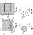
- FIGS. 1-18 depict various embodiments of a system 100 comprising a processing tool 102 and methods of processing semiconductor wafers through such a system.
- FIG. 1 is a block level depiction of one illustrative embodiment of some of the major components of one illustrative embodiment of a system 100 disclosed herein.
- the system 100 comprises a processing tool 102 with a small-volume process chamber 130 (see FIG. 2 ), a wafer lift system 104 , a wafer chuck moving system 105 , a wafer handling system 106 and a system controller 108 .
- the processing tool 102 may be used as one part of an elaborate fabrication process to manufacture semiconductor wafers into functional semiconductor devices and various integrated circuit products.
- the illustrative embodiment of the system 100 shown in FIG. 1 only includes a single processing tool 102 , a single wafer lift system 104 , a single wafer chuck moving system 105 , a single wafer handling system 106 and a single controller 108 .
- the depiction of such single entities is representative in nature in that a real-world system 100 may include any desired number of each of the five components that may be arranged in a variety of different configurations.
- a system 100 may include a plurality of individual processing tools 102 , each of which is serviced by a single wafer lift system 104 , a single wafer chuck moving system 105 , a single wafer handling system 106 and one or more controllers 108 , all of which may be housed in one or more cabinets.
- each of the processing tools 102 may be serviced by a dedicated single wafer lift system 104 , a dedicated wafer chuck moving system 105 , a dedicated single wafer handling system 106 and a single dedicated controller 108 .
- the controller(s) may be a stand-alone computer(s) or it (or they) may be housed in any of the components of the system 100 or dispersed in the various components of the system 100 .
- the subject matter disclosed herein should not be considered to be limited to any particular form or arrangement of the various components of the systems disclosed herein.
- the terms “wafer” and “substrate” are used interchangeably herein, and both are directed to any form or shape of any semiconductor material wherein integrated circuits (of any type, shape or form) are formed on the wafer or substrate.
- the substrate 118 is simplistically depicted as being comprised of a single bulk semiconductor material.
- the presently disclosed subject matter should not be considered to be limited to this illustrative example of the substrate 118 .
- the substrate 118 may be an FDSOI (fully depleted silicon-on-insulator) substrate.
- such an SOI substrate comprises a base semiconductor substrate, a buried insulation layer (sometime referred to as a “BOX” layer when the insulation layer comprises silicon dioxide) positioned on the base substrate and an active layer comprised of a semiconducting material positioned on the buried layer of insulating material.
- the base semiconducting substrate may comprise silicon
- the buried insulation layer may comprise silicon dioxide
- the active layer may comprise silicon and/or other semiconductor materials.
- the base semiconducting substrate and the active layer may be made of any of a variety of different semiconductor materials, and the materials for the base semiconducting substrate and the active layer need not be made of the same material in all applications, but such a situation may occur in some applications.
- the terms “substrate”, “semiconductor substrate” or “wafer” should be understood to cover all semiconducting materials and all forms of such materials.
- FIGS. 2-8 depict various views of one illustrative embodiment of a processing tool 102 with a small-volume process chamber 130 that may be employed in the systems 100 disclosed herein.
- the process chamber 130 is sized such that only a single wafer may 118 be processed in the process chamber 130 during a given processing cycle.
- the processing tool 102 has an overall generally rectangular, three-dimensional configuration with a length (“L”), a width (“W) and a height (“H”) (see FIG. 7 ).
- L length
- W width
- H height
- the absolute values of the length, width and height measurements may vary depending upon the particular application. Of course, all of the drawings in the present application are not to scale.
- FIG. 2 is a cross-sectional view of one illustrative embodiment of the processing tool 102 disclosed herein.
- the processing tool 102 is adapted to process only one single wafer 118 during a given processing cycle.
- the processing tool 102 comprises a body 112 , a chamber door 114 , a wafer chuck 116 and an internal small-volume processing chamber 130 .
- the wafer chuck 116 is adapted to have the wafer 118 that is to be processed in the chamber 130 positioned on the wafer chuck 116 .
- the floor of the process chamber 130 comprises a notched chuck recess 120 with a partial circular end surface 120 X.
- the notched chuck recess 120 is adapted to receive the wafer chuck 116 when the wafer chuck 116 is positioned at the wafer processing position within the chamber 130 .
- the body 112 comprises a top surface 112 W, a bottom surface 112 X, a back surface 112 Y and a front surface 112 Z.
- the chamber door 114 has a front surface 114 X and a back surface 114 Y.
- the chamber door 114 is adapted to sealingly engage the front surface 112 Z of the processing tool 102 /process chamber 130 so as to effectively close and seal the chamber 130 .
- the wafer chuck 116 is formed integral with the back surface of the chamber door 114 .
- the attachment of the wafer chuck 116 to the chamber door 114 may be accomplished by a variety of techniques (e.g., welding, a bolted connection, etc.).
- FIG. 3 is a simplistic plan view of only the bottom floor of the process chamber 130 .
- the notched chuck recess 120 formed in the floor of the chamber 130 is depicted in this view.
- FIG. 4 is a simplistic plan view of the wafer chuck 116 /chamber door 114 with the wafer 118 in position on the wafer chuck 116 .
- the wafer chuck 116 comprises a partial circular end surface 116 X that is adapted to be positioned adjacent the circular end surface 120 X of the notched chuck recess 120 when the wafer chuck 116 is positioned at its fully-inserted, wafer-processing position within the process chamber 130 .
- FIG. 5 is a simplistic plan view of the wafer chuck 116 /chamber door 114 without the wafer 118 .
- a plurality of lift pin holes 124 are provided in the wafer chuck 116 so as to permit a plurality of wafer lift pins 140 (discussed below) of the wafer lift system 104 to pass through the lift pin holes 124 .
- an upper surface 140 S of the wafer lift pins 140 is adapted to engage a bottom surface of a wafer 118 that is positioned on or above an upper surface of the wafer chuck 116 when the wafer chuck 116 is in its chuck wafer transfer position (see, e.g., FIGS. 6-7 (wherein a wafer 118 may or not be present).
- the number and size of the lift pin holes 124 may vary depending upon the particular application. In the depicted example, three such lift pin holes 124 are provided in the wafer chuck 116 .
- the wafer chuck 116 may be a heated chuck that is capable of heating the wafer 118 by, for example, electrical resistance heating, or it may be a non-heated chuck.
- FIGS. 6 and 7 are simplistic plan and side views, respectively, depicting the chamber door 114 in its open position whereby the wafer chuck 116 is in its chuck wafer transfer position without a wafer 118 in place on the wafer chuck 116 .
- FIG. 8 is a simplistic plan view depicting the chamber door 114 in its closed position whereby the wafer chuck 116 is in its wafer processing position without the wafer 118 in position on the wafer chuck 116 .
- the wafer chuck moving system 105 comprises a plurality of support rods 132 that are operatively coupled (directly or indirectly) to the wafer chuck 116 , and means for moving the wafer chuck 116 from the wafer processing position within the process chamber 130 to the chuck wafer transfer position.
- a wafer 118 may be transferred to or from the wafer chuck 116 by positioning the wafer on the wafer lift pins 140 when the wafer lift pins 140 have been extended through the lift pin openings 124 .
- the plurality of support rods 132 are operatively coupled to the body 112 and the chamber door 114 .
- the support rods 132 along with the means of actuating the support rods 132 , are adapted to provide the means for moving the wafer chuck 116 from its wafer-processing position ( FIG. 8 ), wherein the chamber door 114 is sealingly engaged to the process chamber 130 , to retracted or open chuck wafer transfer position ( FIG. 6 or 7 ) whereby a wafer 118 may be positioned on or removed from the wafer chuck 116 .
- FIG. 8 the wafer-processing position
- FIG. 6 or 7 retracted or open chuck wafer transfer position
- FIGS. 6 and 7 depict the position of the support rods 132 (in dashed lines) with the chamber door 114 in its closed position as well as the position of the wafer chuck 116 in its wafer processing position (without the wafer 118 ).
- the support rods 132 are positioned within recesses or channels (not shown) formed in the body 112 of the processing tool 102 that are adapted to receive the support rods 132 .
- the position of the support rods 132 with the wafer chuck in its chuck wafer-transfer position are shown in FIGS. 6 and 7 .
- the components of the wafer chuck moving system 105 may comprise any of a variety of traditional electro-mechanical actuation means or devices.
- the wafer chuck moving system 105 may include means for actuating the support rods 132 that may comprise one or more hydraulically or pneumatically actuated cylinders (not shown), one or more position detecting switches (e.g., limit switches) and one or more electrical motors (not shown) that are operatively coupled (directly or indirectly) to the support rods 132 so as to move them from the retracted position to the extended position, and vice-versa.
- the structure, function and operation of such wafer chuck moving systems 105 are well known to those skilled in the art.
- the combination of the wafer lift system 104 and the wafer handling system 106 is adapted to either (1) position a wafer 118 that is to be processed in the chamber 130 on the wafer chuck 116 or (2) remove a wafer 118 that was previously processed in the chamber 130 from the upper surface of the wafer chuck 116 .
- FIG. 9 is a simplistic plan view of one illustrative embodiment of a novel system 100 disclosed herein wherein one illustrative embodiment of the wafer handling system 106 is depicted.
- the controller 108 and the wafer lift system 104 are not depicted in FIG. 9 .
- FIG. 10 is a side view of the illustrative embodiment of the system 100 shown in FIG. 9 .
- the controller 108 is not depicted in FIG. 10 , but the wafer lift system 104 is simplistically depicted in FIG. 10 .
- the simplistically depicted wafer handling system 106 comprises a robotic arm 137 that comprises a wafer gripper assembly 138 that is operatively coupled to an end of the robotic arm 137 .
- the combination of the robotic arm 137 and the wafer gripper assembly 138 is adapted to grasp and retrieve a single wafer 118 from a wafer carrier (not shown) that contains a plurality of individual wafers 118 that are to be processed—one by one—in the process chamber 130 .
- the combination of the robotic arm 137 and the wafer gripper assembly 138 is also adapted to (1) position and place a particular grasped wafer 118 on the wafer lift pins 140 when the wafer lift pins 140 are in their extended lift pin wafer transfer position, and (2) grasp and remove a wafer 118 from the extended wafer lift pins 140 after that wafer was previously processed in the chamber 130 and return it to the wafer carrier.
- the wafer handling system 106 depicted herein may have a structure and functional capabilities equivalent to any of a variety of different wafer handling systems that are commercially available in the marketplace. As noted above, the wafer handling system 106 may be representative of one or more physical wafer handling systems, each of which is adapted to serve one or more process chambers 130 in an overall system 100 .
- FIGS. 10 and 11 simplistically depict one illustrative embodiment of a wafer lift system 104 that may be employed in various systems disclosed herein.
- the wafer lift system 104 comprises a plurality of wafer lift pins 140 , each of which have an upper wafer-engaging surface 140 S.
- Each of the wafer lift pins 140 is adapted to be extended through a corresponding one of the lift pin holes 124 in the chuck 116 .
- the wafer lift pins 140 may be moved from an extended position (shown in FIG. 10 ) whereby the upper surfaces 140 S of the wafer lift pins 140 are positioned in a plane 141 —the lift pin wafer transfer position.
- the wafer transfer system 106 may be actuated to either (1) position a wafer 118 (that is to be processed in the process chamber 130 ) on the extended wafer lift pins 140 or (2) lift a wafer 118 (that was previously processed in the processing tool 102 ) off of the extended wafer lift pins 140 and position that processed wafer 118 in a wafer carrier (not shown).
- the wafer lift pins 140 are also adapted to be moved to a retracted position whereby the upper surfaces 140 S of the lift pins 140 are in a plane 142 that is at least below the level at which the wafer lift pins 140 are no longer in a position to interfere with the movement of other system components, e.g., so as not to interfere with the chamber door 114 being moved from a closed position to an open position, or vice-versa, with respect to the process chamber 130 .
- the wafer lift pins 140 may be fully retracted such that the wafer lift pins 140 are completely retracted to a position within a housing (not shown) of the wafer lift system 104 .
- the number and size of the wafer lift pins 140 may vary depending upon the particular application. In the disclosed embodiment, three illustrative wafer lift pins 140 are depicted. As will be appreciated by those skilled in the art after a complete reading of the present application, since the wafer lift system 104 disclosed herein is physically positioned outside of process chamber 130 , the lift pins 140 will be moved from their retracted position to their extended position only when the wafer chuck 116 is in its wafer-transfer position as shown in FIG. 10 .
- the wafer lift system 104 depicted herein may have a structure and functional capabilities equivalent to any of a variety of different wafer lift systems that are commercially available in the marketplace.
- the wafer lift pins 140 may be actuated from a retracted position (wherein the surfaces 140 S are at or below the plane 142 ) to an extended position (wherein the surfaces 140 S are at the plane 141 and the wafer lift pins 140 are in the lift pin wafer transfer position), and vice-versa, by using any of a variety of traditional electro-mechanical actuation means and devices.
- the means for actuating the wafer lift pins 140 may comprise one or more hydraulically or pneumatically actuated cylinders (not shown), one or more position detecting switches (e.g., limit switches) and/one or more electrical motors (not shown) that are operatively coupled (directly or indirectly) to the wafer lift pins 140 so as to move them from the retracted position to the extended position, and vice-versa.
- position detecting switches e.g., limit switches
- electrical motors not shown
- FIG. 11 simplistically depicts one illustrative example of a means by which the wafer lift pins 140 may be moved from an extended position to a retracted position and vice-versa.
- the plurality of wafer lift pins 140 are operatively coupled to a moveable block 144 positioned within a housing 147 .
- a plurality of fixed guide rods 146 are a coupled to the housing 147 .
- Fixed guide rods 146 extend through openings 148 formed in the moveable block 144 .
- a rack 150 is fixed to the side of the moveable block 144 .
- the rack 150 comprises a plurality of teeth 151 . Also shown in FIG.
- FIG. 11 is a schematically depicted electric motor 154 (e.g., a stepper motor) that is in a fixed position within the housing 147 .
- An illustrative pinion 152 is operatively coupled to the shaft (not separately shown) of the motor 154 .
- the pinion 152 comprises a plurality of teeth 153 (only one of which is shown).
- the teeth 153 on the pinion 152 are adapted to mesh with the teeth 151 on the rack 150 .
- the moveable block 144 travels up or down (depending upon the direction of rotation of the pinion 152 ) on the fixed guide rods 146 , thereby causing the attached wafer lift pins 140 to be moved to their extended or retracted positions.
- the illustrative controller 108 shown in FIG. 1 is intended to be a broad representation of any type of one or more computing devices that may be programmed so as to perform the various functions described herein.
- the controller 108 is a computer programmed with software to implement the functions described herein.
- the functions described for the controller 108 may be performed by one or more controllers spread through the system 100 .
- the controller 108 may be a fab level controller that is used to control processing operations throughout all or a portion of a semiconductor manufacturing facility.
- the controller 108 may be a lower level computer that controls only portions or cells of the manufacturing facility.
- the controller 108 may be a stand-alone device (or a plurality of stand-alone devices that operatively function with one another), or it may reside on or among any of the processing tool 102 , the wafer lift system 104 and/or the wafer handling system 106 .
- a hardware controller (not shown) designed to implement the particular functions may also be used.
- the processing tool 102 disclosed herein may be employed to perform any type of processing operation.
- the processing tool 102 may be adapted to perform an anneal process in the processing chamber 130 .
- the processing tool 102 may be employed to perform a high-pressure anneal process in the process chamber 130 using a process gas that comprises deuterium or a halogen as at least one of the process gasses during the anneal process (an HPD2 anneal process).
- the HPD2 anneal process may be performed at a pressure of about 0.5-3 MPa and at a temperature of about 300-500° C.
- Traditional HPD2 anneal tools are batch furnaces.
- the volume of the processing chamber 130 is made as small as is reasonably practicable so as to reduce the volume of process gas, e.g., deuterium, that is required to generate the high-pressure processing condition during the anneal process.
- process gas e.g., deuterium
- such wafer lift systems are typically positioned within the processing chamber, thereby causing an inside dimension of the process chamber to be large enough (at least in the vertical direction) to accommodate the wafer lifting system hardware and movement of such hardware during wafer lifting processes.
- these factors tend to increase the volume of the prior art process chamber beyond what is actually necessary to perform the processing operation.
- This excess processing volume must be filled with processing gas to perform the desired processing operation.
- such single-wafer prior art processing tools may have a process chamber with a volume of about 10-30 liters.
- the volume of the process chamber 130 may be specifically designed to have a relatively small volume as compared to the process chambers in prior art annealing tools.
- the internal volume of the process chamber 130 disclosed herein may be about 0.2-5 liters.
- the absolute volume of the pressure chamber 130 may vary depending upon the particular application and the size of the wafers 118 processed therein.
- FIGS. 12-18 depict various views of another illustrative embodiment of the processing tool 102 with a small-volume process chamber 130 that may be employed in the systems 100 disclosed herein.
- this embodiment of the processing tool 102 comprises a slot 170 that permits or blocks access to the process chamber 130 .
- an upper door recess 174 and a lower door recess 176 are formed in the body 112 .
- the upper door recess 174 and the lower door recess 176 are adapted to receive a sliding door 172 that may be actuated to open or close the slot 170 .
- FIG. 12 depict various views of another illustrative embodiment of the processing tool 102 with a small-volume process chamber 130 that may be employed in the systems 100 disclosed herein.
- this embodiment of the processing tool 102 comprises a slot 170 that permits or blocks access to the process chamber 130 .
- an upper door recess 174 and a lower door recess 176 are formed in the body 112 .
- the sliding door 172 is depicted in its raised position whereby slot 170 is open and the wafer chuck 116 may be inserted into or withdrawn from the process chamber 130 .
- the process chamber 130 is adapted to process only a single wafer 118 during a given processing cycle.
- FIG. 13 is a simplistic plan view of just the bottom or floor of the chamber 130 with the wafer chuck 116 removed.
- the lower door recess 176 is also depicted in FIG. 13 .
- FIG. 14 is a simplistic plan view of the wafer chuck 116 with the wafer 118 in position on the chuck 116 .
- a plurality of attachment structures 116 A are coupled to the wafer chuck 116 .
- the attachment structures 116 A may be components that are physically separate from the wafer chuck 116 , or they may be formed as an integral part of the wafer chuck 116 .
- the attachment structures 116 A are adapted to be operatively coupled to the above-described support rods 132 .
- the attachment structures 116 A may simply be an extension of the support rods 132 .
- FIG. 15 is a simplistic plan view of this illustrative example of a wafer chuck 116 with the wafer 118 removed.
- a plurality of lift pin holes 124 are provided in the wafer chuck 116 so as to permit the above-described wafer lift pins 140 of the wafer lift system 104 to pass through the lift pin holes 124 and thereby engage the bottom of a previously processed wafer 118 that is positioned on the upper surface of the wafer chuck 116 when the wafer chuck 116 is moved from its wafer processing position within the process chamber 130 to its chuck wafer transfer position by actuation of the wafer chuck moving system 105 .
- FIGS. 16 and 17 are simplistic plan and side views, respectively, depicting the wafer chuck 116 in its chuck wafer-transfer position without a wafer 118 in place on the wafer chuck 116 .
- FIG. 18 is a simplistic plan view depicting the wafer chuck 116 in its wafer processing position within the chamber 130 without the wafer 118 in place on the wafer chuck 116 .
- the upper door recess 172 and the lower door recess 176 are shown in FIG. 17 .
- FIG. 17 also depicts the sliding door 172 in its closed position whereby the slot 170 is blocked and access to the chamber 130 is blocked. Note that in its closed position, a lower end 172 A of the sliding door 172 is positioned within the lower door recess 176 .
- the plurality of support rods 132 are operatively coupled to the body 112 and the attachment structures 116 A.
- the support rods 132 along with the means of actuating the support rods 132 , are adapted to enable the movement of the wafer chuck 118 from in its wafer processing position within the chamber 130 ( FIG. 18 ) to its chuck wafer transfer position outside of the process chamber 130 ( FIG. 16 or 17 ).
- the position of the support rods 132 with the sliding door 172 closed and the wafer chuck in wafer processing position within the process chamber 130 are shown in FIG. 18 .
- the support rods 132 are positioned within recesses or channels (not shown) in the body 112 that are adapted to receive the support rods 132 .
- the support rods 132 may be actuated using various means as previously described.
- the sliding door 170 may be actuated from a retracted position ( FIG. 12 ) whereby the slot 170 is open, to an extended position ( FIG. 17 ) whereby the slot 170 is closed, and vice-versa, by using any of a variety of traditional electro-mechanical actuation means that are well known to those skilled in the art.
- the means for actuating the sliding door 170 may comprise one or more hydraulically or pneumatically actuated cylinders (not shown), one or more position detecting switches (e.g., limit switches) and one or more electrical motors (not shown) that are operatively coupled (directly or indirectly) to the sliding door 170 so as to move it from the retracted position to the extended position, and vice-versa.
- This embodiment of the processing tool 102 is adapted to interact with the above-described wafer lift system 104 and wafer handling system 106 in substantially the same manner as does the previous embodiment.
- the combination of the wafer lift system 104 and the wafer handling system 106 is adapted to either (1) position a wafer 118 that is to be processed in the chamber 130 on the wafer chuck 116 or (2) remove a wafer 118 that was previously processed in the chamber 130 from the wafer chuck 116 .
Abstract
Description
-
- 1. Move the
wafer chuck 116 to its chuck wafer transfer position outside of the process chamber 130 (e.g.,FIG. 6-7 ;FIG. 16-17 ); - 2. With the
wafer chuck 116 in its chuck wafer transfer position, actuate thewafer lift system 104 to extend the wafer lift pins 140 through the correspondingopenings 124 in thewafer chuck 116 until the wafer lift pins 140 reach their extended position whereby theupper surfaces 140S of the wafer lift pins 140 are located in theplane 141—the lift pin wafer transfer position (see, e.g.,FIG. 10 ); - 3. Actuate the
wafer transfer system 106 to grasp asingle wafer 118 from the wafer carrier and place the graspedwafer 118 on the extended wafer lift pins 140; - 4. Actuate the
gripper 138 so as to disengage from engagement with the wafer, thereby leaving thewafer 118 in place on theupper surfaces 140S of the wafer lift pins 140 with the wafer lift pins 140 in their extended wafer transfer position; - 5. Withdraw the
robotic arm 137/gripper 138 to a position where it will not interfere with movement of thewafer chuck 116 or other system components; - 6. Actuate the
wafer lift system 104 to move the wafer lift pins 140 back through theopenings 124 in thewafer chuck 116 to their retracted position, whereby theupper surfaces 140S of thepins 140 are in a plane, whereby the wafer lift pins 140 do not interfere with any further movement of system components or wafer transfer operations. This operation results in the placement of thewafer 118 to be processed in theprocess chamber 130 on the upper surface of thewafer chuck 116; - 7. Actuate the wafer chuck movement system to move the
wafer chuck 116, with thewafer 118 positioned thereon, to the wafer processing position within theprocess chamber 130 in the processing tool 102 (see, e.g.,FIGS. 2 and 12 (the slidingdoor 170 will be closed while processing the wafer 118); - 8. Performing processing operations on the
wafer 118 within thechamber 130 until completion; - 9. Actuate the wafer chuck movement system to move the
wafer chuck 116, with the now-processedwafer 118 positioned thereon, to the chuck wafer transfer position of the wafer chuck 116 (see, e.g.,FIGS. 6-7 and 16-17 ); - 10. With the
wafer chuck 116 in its wafer transfer position, actuate thewafer lift system 104 to extend the wafer lift pins 140 through theopenings 124 in thewafer chuck 116 and thereby engage the bottom of the now-processedwafer 118. Continue moving the wafer lift pins 140 upward until the wafer lift pins 140 are in their extended position whereby theupper surfaces 140S of the wafer lift pins 140 are located in theplane 141—the lift pin wafer transfer position (see, e.g.,FIG. 10 ); and - 11. Actuate the
wafer transfer system 106 to grasp the now-processedwafer 118, lift the now-processed wafer off of the extended wafer lift pins 140 and return the now-processedwafer 118 to the wafer carrier.
Of course, as will be appreciated by those skilled in the art after a complete reading of the present application, many of the actions described immediately above may be performed at the same time and need not necessarily be entirely completed before another action is taken. For example, thewafer lift system 104 may be actuated to move the wafer lift pins 140 through theopenings 124 in thewafer chuck 116 and toward their final extended wafer transfer position (surfaces 140S in plane 141) while thewafer handling system 106 is moving awafer 118 that is to be processed in thechamber 130 toward thewafer chuck 116.
- 1. Move the
Claims (19)
Priority Applications (4)
| Application Number | Priority Date | Filing Date | Title |
|---|---|---|---|
| US16/225,540 US10770338B2 (en) | 2018-12-19 | 2018-12-19 | System comprising a single wafer, reduced volume process chamber |
| DE102019217665.8A DE102019217665A1 (en) | 2018-12-19 | 2019-11-18 | COMPREHENSIVE SYSTEM A SINGLE WAFFER PROCESS CHAMBER WITH REDUCED VOLUME |
| TW108141942A TWI756587B (en) | 2018-12-19 | 2019-11-19 | System comprising a single wafer, reduced volume process chamber |
| CN201911133062.9A CN111341721A (en) | 2018-12-19 | 2019-11-19 | System including a single wafer, reduced volume processing chamber |
Applications Claiming Priority (1)
| Application Number | Priority Date | Filing Date | Title |
|---|---|---|---|
| US16/225,540 US10770338B2 (en) | 2018-12-19 | 2018-12-19 | System comprising a single wafer, reduced volume process chamber |
Publications (2)
| Publication Number | Publication Date |
|---|---|
| US20200203208A1 US20200203208A1 (en) | 2020-06-25 |
| US10770338B2 true US10770338B2 (en) | 2020-09-08 |
Family
ID=70969341
Family Applications (1)
| Application Number | Title | Priority Date | Filing Date |
|---|---|---|---|
| US16/225,540 Active 2039-01-18 US10770338B2 (en) | 2018-12-19 | 2018-12-19 | System comprising a single wafer, reduced volume process chamber |
Country Status (4)
| Country | Link |
|---|---|
| US (1) | US10770338B2 (en) |
| CN (1) | CN111341721A (en) |
| DE (1) | DE102019217665A1 (en) |
| TW (1) | TWI756587B (en) |
Families Citing this family (1)
| Publication number | Priority date | Publication date | Assignee | Title |
|---|---|---|---|---|
| US11769673B2 (en) * | 2021-02-15 | 2023-09-26 | Globalfoundries U.S. Inc. | Semiconductor wafer processing system |
Citations (10)
| Publication number | Priority date | Publication date | Assignee | Title |
|---|---|---|---|---|
| US6007675A (en) | 1996-07-09 | 1999-12-28 | Gamma Precision Technology, Inc. | Wafer transfer system and method of using the same |
| US6146463A (en) * | 1998-06-12 | 2000-11-14 | Applied Materials, Inc. | Apparatus and method for aligning a substrate on a support member |
| US6719516B2 (en) | 1998-09-28 | 2004-04-13 | Applied Materials, Inc. | Single wafer load lock with internal wafer transport |
| US20060137609A1 (en) | 2004-09-13 | 2006-06-29 | Puchacz Jerzy P | Multi-single wafer processing apparatus |
| US20140299681A1 (en) * | 2013-04-05 | 2014-10-09 | Dhritiman S. Kashyap | Cascade design showerhead for transient uniformity |
| US20150011093A1 (en) * | 2013-07-08 | 2015-01-08 | Lam Research Corporation | Ion beam etching system |
| US20150126042A1 (en) * | 2013-11-07 | 2015-05-07 | Novellus Systems, Inc. | Soft landing nanolaminates for advanced patterning |
| US20160111318A1 (en) * | 2013-05-23 | 2016-04-21 | Nikon Corporation | Substrate holding method, substrate holding apparatus, exposure apparatus and exposure method |
| US20170011932A1 (en) | 2015-07-06 | 2017-01-12 | Globalfoundries Inc. | High-pressure anneal |
| US20170221740A1 (en) * | 2016-01-29 | 2017-08-03 | Lam Research Corporation | Methods and apparatuses for estimating on-wafer oxide layer reduction effectiveness via color sensing |
Family Cites Families (7)
| Publication number | Priority date | Publication date | Assignee | Title |
|---|---|---|---|---|
| US6610150B1 (en) * | 1999-04-02 | 2003-08-26 | Asml Us, Inc. | Semiconductor wafer processing system with vertically-stacked process chambers and single-axis dual-wafer transfer system |
| WO2010067159A2 (en) * | 2008-12-12 | 2010-06-17 | Applied Materials, Inc. | Integration of a processing bench in an inline coating system |
| JP6411172B2 (en) * | 2014-10-24 | 2018-10-24 | 東京エレクトロン株式会社 | Substrate processing method, substrate processing apparatus, and storage medium |
| WO2017062136A1 (en) * | 2015-10-04 | 2017-04-13 | Applied Materials, Inc. | Reduced volume processing chamber |
| CN107564830B (en) * | 2016-06-30 | 2020-10-27 | 无锡华瑛微电子技术有限公司 | Semiconductor processing equipment group and semiconductor processing equipment |
| KR20180086715A (en) * | 2017-01-23 | 2018-08-01 | 어플라이드 머티어리얼스, 인코포레이티드 | Transfer module, substrate processing system having the same and substrate processing mehtod using the same |
| US11201078B2 (en) * | 2017-02-14 | 2021-12-14 | Applied Materials, Inc. | Substrate position calibration for substrate supports in substrate processing systems |
-
2018
- 2018-12-19 US US16/225,540 patent/US10770338B2/en active Active
-
2019
- 2019-11-18 DE DE102019217665.8A patent/DE102019217665A1/en active Pending
- 2019-11-19 TW TW108141942A patent/TWI756587B/en active
- 2019-11-19 CN CN201911133062.9A patent/CN111341721A/en active Pending
Patent Citations (10)
| Publication number | Priority date | Publication date | Assignee | Title |
|---|---|---|---|---|
| US6007675A (en) | 1996-07-09 | 1999-12-28 | Gamma Precision Technology, Inc. | Wafer transfer system and method of using the same |
| US6146463A (en) * | 1998-06-12 | 2000-11-14 | Applied Materials, Inc. | Apparatus and method for aligning a substrate on a support member |
| US6719516B2 (en) | 1998-09-28 | 2004-04-13 | Applied Materials, Inc. | Single wafer load lock with internal wafer transport |
| US20060137609A1 (en) | 2004-09-13 | 2006-06-29 | Puchacz Jerzy P | Multi-single wafer processing apparatus |
| US20140299681A1 (en) * | 2013-04-05 | 2014-10-09 | Dhritiman S. Kashyap | Cascade design showerhead for transient uniformity |
| US20160111318A1 (en) * | 2013-05-23 | 2016-04-21 | Nikon Corporation | Substrate holding method, substrate holding apparatus, exposure apparatus and exposure method |
| US20150011093A1 (en) * | 2013-07-08 | 2015-01-08 | Lam Research Corporation | Ion beam etching system |
| US20150126042A1 (en) * | 2013-11-07 | 2015-05-07 | Novellus Systems, Inc. | Soft landing nanolaminates for advanced patterning |
| US20170011932A1 (en) | 2015-07-06 | 2017-01-12 | Globalfoundries Inc. | High-pressure anneal |
| US20170221740A1 (en) * | 2016-01-29 | 2017-08-03 | Lam Research Corporation | Methods and apparatuses for estimating on-wafer oxide layer reduction effectiveness via color sensing |
Non-Patent Citations (4)
| Title |
|---|
| Andrieu, SiGe Channel and Layout EFFETS: Basics Brochure, Cea Tech. |
| Applied Vantage Vulcan RTP Brochure, Jun. 29, 2011. |
| Horstmann et al., "Integration and Optimization of Embedded-SiGe, Compressive and Tensile Stressed Liner Films, and Stress Memorization in Advanced SOI CMOS Technologies," 2005 IEEE. |
| Pidin et al, "A Novel Strain Enhanced CMOS Architecture Using Selectively Deposited High Tensile and High Compressive Silicon Nitride Films," 2004 IEEE. |
Also Published As
| Publication number | Publication date |
|---|---|
| CN111341721A (en) | 2020-06-26 |
| US20200203208A1 (en) | 2020-06-25 |
| DE102019217665A1 (en) | 2020-06-25 |
| TW202044451A (en) | 2020-12-01 |
| TWI756587B (en) | 2022-03-01 |
Similar Documents
| Publication | Publication Date | Title |
|---|---|---|
| KR102417929B1 (en) | Apparatus for substrate processing | |
| US9443749B2 (en) | Vacuum processing apparatus | |
| US8403613B2 (en) | Bypass thermal adjuster for vacuum semiconductor processing | |
| US6331095B1 (en) | Transportation system and processing apparatus employing the transportation system | |
| TW420839B (en) | Multi-position load lock chamber | |
| TWI623055B (en) | Processing systems, apparatus, and methods adapted to process substrates in electronic device manufacturing | |
| KR101736854B1 (en) | Substrate treating apparatus | |
| US20160035601A1 (en) | Bake unit, substrate treating apparatus including the unit, and substrate treating method | |
| JP2010192855A (en) | Substrate processing apparatus | |
| WO2007103870A2 (en) | Bypass thermal adjuster for vacuum semiconductor processing | |
| CN107731710B (en) | Loading station for substrate processing system and substrate processing tool | |
| US10770338B2 (en) | System comprising a single wafer, reduced volume process chamber | |
| JPH0487785A (en) | Base board conveyer | |
| JP2013102235A (en) | Substrate processing apparatus | |
| KR20190070280A (en) | Teaching method of conveying apparatus | |
| KR20190093693A (en) | Apparatus and Methods for Wafer Rotation to Improve Spatial ALD Process Uniformity | |
| US20170352562A1 (en) | Dodecadon transfer chamber and processing system having the same | |
| US11081376B2 (en) | Substrate processing apparatus, transfer module, and coupling module | |
| TWI734180B (en) | Methods, apparatus, and manufacturing system for finfet devices with reduced parasitic capacitance | |
| US20210272832A1 (en) | Reduced footprint wafer handling platform | |
| US11309199B2 (en) | Substrate transfer apparatus and substrate transfer method | |
| KR101383248B1 (en) | High speed substrate processing system | |
| WO2020137646A1 (en) | Substrate processing device | |
| WO2023162355A1 (en) | Substrate treatment method and substrate treatment device | |
| KR20180021263A (en) | Substrate cooling apparatus and substrate treating facility uncluding the unit |
Legal Events
| Date | Code | Title | Description |
|---|---|---|---|
| AS | Assignment |
Owner name: GLOBALFOUNDRIES INC., CAYMAN ISLANDS Free format text: ASSIGNMENT OF ASSIGNORS INTEREST;ASSIGNORS:PETHE, WIELAND;NOACK, DIRK;REEL/FRAME:047817/0498 Effective date: 20181219 |
|
| FEPP | Fee payment procedure |
Free format text: ENTITY STATUS SET TO UNDISCOUNTED (ORIGINAL EVENT CODE: BIG.); ENTITY STATUS OF PATENT OWNER: LARGE ENTITY |
|
| STPP | Information on status: patent application and granting procedure in general |
Free format text: NOTICE OF ALLOWANCE MAILED -- APPLICATION RECEIVED IN OFFICE OF PUBLICATIONS |
|
| STCF | Information on status: patent grant |
Free format text: PATENTED CASE |
|
| AS | Assignment |
Owner name: GLOBALFOUNDRIES U.S. INC., CALIFORNIA Free format text: ASSIGNMENT OF ASSIGNORS INTEREST;ASSIGNOR:GLOBALFOUNDRIES INC.;REEL/FRAME:054633/0001 Effective date: 20201022 |
|
| AS | Assignment |
Owner name: GLOBALFOUNDRIES U.S. INC., NEW YORK Free format text: RELEASE BY SECURED PARTY;ASSIGNOR:WILMINGTON TRUST, NATIONAL ASSOCIATION;REEL/FRAME:056987/0001 Effective date: 20201117 |
|
| MAFP | Maintenance fee payment |
Free format text: PAYMENT OF MAINTENANCE FEE, 4TH YEAR, LARGE ENTITY (ORIGINAL EVENT CODE: M1551); ENTITY STATUS OF PATENT OWNER: LARGE ENTITY Year of fee payment: 4 |