US10699628B2 - Display system and vehicle - Google Patents
Display system and vehicle Download PDFInfo
- Publication number
- US10699628B2 US10699628B2 US15/596,138 US201715596138A US10699628B2 US 10699628 B2 US10699628 B2 US 10699628B2 US 201715596138 A US201715596138 A US 201715596138A US 10699628 B2 US10699628 B2 US 10699628B2
- Authority
- US
- United States
- Prior art keywords
- current
- potential
- transistor
- circuit
- wiring
- Prior art date
- Legal status (The legal status is an assumption and is not a legal conclusion. Google has not performed a legal analysis and makes no representation as to the accuracy of the status listed.)
- Active, expires
Links
- 239000003990 capacitor Substances 0.000 claims description 40
- 230000006870 function Effects 0.000 abstract description 67
- 239000004065 semiconductor Substances 0.000 description 23
- 230000008859 change Effects 0.000 description 17
- 238000010586 diagram Methods 0.000 description 16
- 229910052727 yttrium Inorganic materials 0.000 description 9
- 230000015572 biosynthetic process Effects 0.000 description 7
- 230000014759 maintenance of location Effects 0.000 description 5
- 238000007667 floating Methods 0.000 description 4
- 238000004519 manufacturing process Methods 0.000 description 4
- 230000015556 catabolic process Effects 0.000 description 3
- 238000003384 imaging method Methods 0.000 description 3
- 239000000463 material Substances 0.000 description 3
- 230000009467 reduction Effects 0.000 description 3
- 229910052710 silicon Inorganic materials 0.000 description 3
- 239000010703 silicon Substances 0.000 description 3
- 239000011701 zinc Substances 0.000 description 3
- 230000009471 action Effects 0.000 description 2
- 238000004378 air conditioning Methods 0.000 description 2
- 230000018109 developmental process Effects 0.000 description 2
- 239000000446 fuel Substances 0.000 description 2
- 229910010272 inorganic material Inorganic materials 0.000 description 2
- 239000011147 inorganic material Substances 0.000 description 2
- 239000004973 liquid crystal related substance Substances 0.000 description 2
- 239000011159 matrix material Substances 0.000 description 2
- 229910052684 Cerium Inorganic materials 0.000 description 1
- 229910052779 Neodymium Inorganic materials 0.000 description 1
- 239000004642 Polyimide Substances 0.000 description 1
- 229910052782 aluminium Inorganic materials 0.000 description 1
- QVGXLLKOCUKJST-UHFFFAOYSA-N atomic oxygen Chemical compound [O] QVGXLLKOCUKJST-UHFFFAOYSA-N 0.000 description 1
- 239000003795 chemical substances by application Substances 0.000 description 1
- 239000003086 colorant Substances 0.000 description 1
- 230000008878 coupling Effects 0.000 description 1
- 238000010168 coupling process Methods 0.000 description 1
- 238000005859 coupling reaction Methods 0.000 description 1
- 238000006731 degradation reaction Methods 0.000 description 1
- 230000001419 dependent effect Effects 0.000 description 1
- 238000005516 engineering process Methods 0.000 description 1
- 229910052733 gallium Inorganic materials 0.000 description 1
- 239000011521 glass Substances 0.000 description 1
- 239000001257 hydrogen Substances 0.000 description 1
- 229910052739 hydrogen Inorganic materials 0.000 description 1
- 125000004435 hydrogen atom Chemical class [H]* 0.000 description 1
- 239000012535 impurity Substances 0.000 description 1
- 229910052738 indium Inorganic materials 0.000 description 1
- APFVFJFRJDLVQX-UHFFFAOYSA-N indium atom Chemical compound [In] APFVFJFRJDLVQX-UHFFFAOYSA-N 0.000 description 1
- 230000002401 inhibitory effect Effects 0.000 description 1
- 229910052746 lanthanum Inorganic materials 0.000 description 1
- 239000011368 organic material Substances 0.000 description 1
- 239000001301 oxygen Substances 0.000 description 1
- 229910052760 oxygen Inorganic materials 0.000 description 1
- 230000003071 parasitic effect Effects 0.000 description 1
- 230000002093 peripheral effect Effects 0.000 description 1
- 229910021420 polycrystalline silicon Inorganic materials 0.000 description 1
- 229920001721 polyimide Polymers 0.000 description 1
- 229920005591 polysilicon Polymers 0.000 description 1
- 239000011347 resin Substances 0.000 description 1
- 229920005989 resin Polymers 0.000 description 1
- 230000004044 response Effects 0.000 description 1
- 230000011218 segmentation Effects 0.000 description 1
- 230000003068 static effect Effects 0.000 description 1
- JBQYATWDVHIOAR-UHFFFAOYSA-N tellanylidenegermanium Chemical compound [Te]=[Ge] JBQYATWDVHIOAR-UHFFFAOYSA-N 0.000 description 1
- 229910052719 titanium Inorganic materials 0.000 description 1
- 238000002834 transmittance Methods 0.000 description 1
- 229910052726 zirconium Inorganic materials 0.000 description 1
Images


Classifications
-
- G—PHYSICS
- G09—EDUCATION; CRYPTOGRAPHY; DISPLAY; ADVERTISING; SEALS
- G09G—ARRANGEMENTS OR CIRCUITS FOR CONTROL OF INDICATING DEVICES USING STATIC MEANS TO PRESENT VARIABLE INFORMATION
- G09G3/00—Control arrangements or circuits, of interest only in connection with visual indicators other than cathode-ray tubes
- G09G3/03—Control arrangements or circuits, of interest only in connection with visual indicators other than cathode-ray tubes specially adapted for displays having non-planar surfaces, e.g. curved displays
-
- B—PERFORMING OPERATIONS; TRANSPORTING
- B60—VEHICLES IN GENERAL
- B60K—ARRANGEMENT OR MOUNTING OF PROPULSION UNITS OR OF TRANSMISSIONS IN VEHICLES; ARRANGEMENT OR MOUNTING OF PLURAL DIVERSE PRIME-MOVERS IN VEHICLES; AUXILIARY DRIVES FOR VEHICLES; INSTRUMENTATION OR DASHBOARDS FOR VEHICLES; ARRANGEMENTS IN CONNECTION WITH COOLING, AIR INTAKE, GAS EXHAUST OR FUEL SUPPLY OF PROPULSION UNITS IN VEHICLES
- B60K35/00—Instruments specially adapted for vehicles; Arrangement of instruments in or on vehicles
- B60K35/60—Instruments characterised by their location or relative disposition in or on vehicles
-
- B60K37/02—
-
- G—PHYSICS
- G09—EDUCATION; CRYPTOGRAPHY; DISPLAY; ADVERTISING; SEALS
- G09G—ARRANGEMENTS OR CIRCUITS FOR CONTROL OF INDICATING DEVICES USING STATIC MEANS TO PRESENT VARIABLE INFORMATION
- G09G3/00—Control arrangements or circuits, of interest only in connection with visual indicators other than cathode-ray tubes
- G09G3/20—Control arrangements or circuits, of interest only in connection with visual indicators other than cathode-ray tubes for presentation of an assembly of a number of characters, e.g. a page, by composing the assembly by combination of individual elements arranged in a matrix no fixed position being assigned to or needed to be assigned to the individual characters or partial characters
- G09G3/2092—Details of a display terminals using a flat panel, the details relating to the control arrangement of the display terminal and to the interfaces thereto
-
- G—PHYSICS
- G09—EDUCATION; CRYPTOGRAPHY; DISPLAY; ADVERTISING; SEALS
- G09G—ARRANGEMENTS OR CIRCUITS FOR CONTROL OF INDICATING DEVICES USING STATIC MEANS TO PRESENT VARIABLE INFORMATION
- G09G3/00—Control arrangements or circuits, of interest only in connection with visual indicators other than cathode-ray tubes
- G09G3/20—Control arrangements or circuits, of interest only in connection with visual indicators other than cathode-ray tubes for presentation of an assembly of a number of characters, e.g. a page, by composing the assembly by combination of individual elements arranged in a matrix no fixed position being assigned to or needed to be assigned to the individual characters or partial characters
- G09G3/22—Control arrangements or circuits, of interest only in connection with visual indicators other than cathode-ray tubes for presentation of an assembly of a number of characters, e.g. a page, by composing the assembly by combination of individual elements arranged in a matrix no fixed position being assigned to or needed to be assigned to the individual characters or partial characters using controlled light sources
- G09G3/30—Control arrangements or circuits, of interest only in connection with visual indicators other than cathode-ray tubes for presentation of an assembly of a number of characters, e.g. a page, by composing the assembly by combination of individual elements arranged in a matrix no fixed position being assigned to or needed to be assigned to the individual characters or partial characters using controlled light sources using electroluminescent panels
- G09G3/32—Control arrangements or circuits, of interest only in connection with visual indicators other than cathode-ray tubes for presentation of an assembly of a number of characters, e.g. a page, by composing the assembly by combination of individual elements arranged in a matrix no fixed position being assigned to or needed to be assigned to the individual characters or partial characters using controlled light sources using electroluminescent panels semiconductive, e.g. using light-emitting diodes [LED]
- G09G3/3208—Control arrangements or circuits, of interest only in connection with visual indicators other than cathode-ray tubes for presentation of an assembly of a number of characters, e.g. a page, by composing the assembly by combination of individual elements arranged in a matrix no fixed position being assigned to or needed to be assigned to the individual characters or partial characters using controlled light sources using electroluminescent panels semiconductive, e.g. using light-emitting diodes [LED] organic, e.g. using organic light-emitting diodes [OLED]
- G09G3/3225—Control arrangements or circuits, of interest only in connection with visual indicators other than cathode-ray tubes for presentation of an assembly of a number of characters, e.g. a page, by composing the assembly by combination of individual elements arranged in a matrix no fixed position being assigned to or needed to be assigned to the individual characters or partial characters using controlled light sources using electroluminescent panels semiconductive, e.g. using light-emitting diodes [LED] organic, e.g. using organic light-emitting diodes [OLED] using an active matrix
-
- G—PHYSICS
- G09—EDUCATION; CRYPTOGRAPHY; DISPLAY; ADVERTISING; SEALS
- G09G—ARRANGEMENTS OR CIRCUITS FOR CONTROL OF INDICATING DEVICES USING STATIC MEANS TO PRESENT VARIABLE INFORMATION
- G09G3/00—Control arrangements or circuits, of interest only in connection with visual indicators other than cathode-ray tubes
- G09G3/20—Control arrangements or circuits, of interest only in connection with visual indicators other than cathode-ray tubes for presentation of an assembly of a number of characters, e.g. a page, by composing the assembly by combination of individual elements arranged in a matrix no fixed position being assigned to or needed to be assigned to the individual characters or partial characters
- G09G3/22—Control arrangements or circuits, of interest only in connection with visual indicators other than cathode-ray tubes for presentation of an assembly of a number of characters, e.g. a page, by composing the assembly by combination of individual elements arranged in a matrix no fixed position being assigned to or needed to be assigned to the individual characters or partial characters using controlled light sources
- G09G3/30—Control arrangements or circuits, of interest only in connection with visual indicators other than cathode-ray tubes for presentation of an assembly of a number of characters, e.g. a page, by composing the assembly by combination of individual elements arranged in a matrix no fixed position being assigned to or needed to be assigned to the individual characters or partial characters using controlled light sources using electroluminescent panels
- G09G3/32—Control arrangements or circuits, of interest only in connection with visual indicators other than cathode-ray tubes for presentation of an assembly of a number of characters, e.g. a page, by composing the assembly by combination of individual elements arranged in a matrix no fixed position being assigned to or needed to be assigned to the individual characters or partial characters using controlled light sources using electroluminescent panels semiconductive, e.g. using light-emitting diodes [LED]
- G09G3/3208—Control arrangements or circuits, of interest only in connection with visual indicators other than cathode-ray tubes for presentation of an assembly of a number of characters, e.g. a page, by composing the assembly by combination of individual elements arranged in a matrix no fixed position being assigned to or needed to be assigned to the individual characters or partial characters using controlled light sources using electroluminescent panels semiconductive, e.g. using light-emitting diodes [LED] organic, e.g. using organic light-emitting diodes [OLED]
- G09G3/3275—Details of drivers for data electrodes
-
- G—PHYSICS
- G09—EDUCATION; CRYPTOGRAPHY; DISPLAY; ADVERTISING; SEALS
- G09G—ARRANGEMENTS OR CIRCUITS FOR CONTROL OF INDICATING DEVICES USING STATIC MEANS TO PRESENT VARIABLE INFORMATION
- G09G5/00—Control arrangements or circuits for visual indicators common to cathode-ray tube indicators and other visual indicators
- G09G5/14—Display of multiple viewports
-
- B60K2370/15—
-
- B60K2370/52—
-
- B—PERFORMING OPERATIONS; TRANSPORTING
- B60—VEHICLES IN GENERAL
- B60K—ARRANGEMENT OR MOUNTING OF PROPULSION UNITS OR OF TRANSMISSIONS IN VEHICLES; ARRANGEMENT OR MOUNTING OF PLURAL DIVERSE PRIME-MOVERS IN VEHICLES; AUXILIARY DRIVES FOR VEHICLES; INSTRUMENTATION OR DASHBOARDS FOR VEHICLES; ARRANGEMENTS IN CONNECTION WITH COOLING, AIR INTAKE, GAS EXHAUST OR FUEL SUPPLY OF PROPULSION UNITS IN VEHICLES
- B60K35/00—Instruments specially adapted for vehicles; Arrangement of instruments in or on vehicles
- B60K35/20—Output arrangements, i.e. from vehicle to user, associated with vehicle functions or specially adapted therefor
-
- B—PERFORMING OPERATIONS; TRANSPORTING
- B60—VEHICLES IN GENERAL
- B60K—ARRANGEMENT OR MOUNTING OF PROPULSION UNITS OR OF TRANSMISSIONS IN VEHICLES; ARRANGEMENT OR MOUNTING OF PLURAL DIVERSE PRIME-MOVERS IN VEHICLES; AUXILIARY DRIVES FOR VEHICLES; INSTRUMENTATION OR DASHBOARDS FOR VEHICLES; ARRANGEMENTS IN CONNECTION WITH COOLING, AIR INTAKE, GAS EXHAUST OR FUEL SUPPLY OF PROPULSION UNITS IN VEHICLES
- B60K35/00—Instruments specially adapted for vehicles; Arrangement of instruments in or on vehicles
- B60K35/80—Arrangements for controlling instruments
- B60K35/81—Arrangements for controlling instruments for controlling displays
-
- G—PHYSICS
- G09—EDUCATION; CRYPTOGRAPHY; DISPLAY; ADVERTISING; SEALS
- G09G—ARRANGEMENTS OR CIRCUITS FOR CONTROL OF INDICATING DEVICES USING STATIC MEANS TO PRESENT VARIABLE INFORMATION
- G09G2300/00—Aspects of the constitution of display devices
- G09G2300/04—Structural and physical details of display devices
- G09G2300/0421—Structural details of the set of electrodes
- G09G2300/0426—Layout of electrodes and connections
-
- G—PHYSICS
- G09—EDUCATION; CRYPTOGRAPHY; DISPLAY; ADVERTISING; SEALS
- G09G—ARRANGEMENTS OR CIRCUITS FOR CONTROL OF INDICATING DEVICES USING STATIC MEANS TO PRESENT VARIABLE INFORMATION
- G09G2300/00—Aspects of the constitution of display devices
- G09G2300/08—Active matrix structure, i.e. with use of active elements, inclusive of non-linear two terminal elements, in the pixels together with light emitting or modulating elements
- G09G2300/0809—Several active elements per pixel in active matrix panels
- G09G2300/0814—Several active elements per pixel in active matrix panels used for selection purposes, e.g. logical AND for partial update
-
- G—PHYSICS
- G09—EDUCATION; CRYPTOGRAPHY; DISPLAY; ADVERTISING; SEALS
- G09G—ARRANGEMENTS OR CIRCUITS FOR CONTROL OF INDICATING DEVICES USING STATIC MEANS TO PRESENT VARIABLE INFORMATION
- G09G2300/00—Aspects of the constitution of display devices
- G09G2300/08—Active matrix structure, i.e. with use of active elements, inclusive of non-linear two terminal elements, in the pixels together with light emitting or modulating elements
- G09G2300/0809—Several active elements per pixel in active matrix panels
- G09G2300/0842—Several active elements per pixel in active matrix panels forming a memory circuit, e.g. a dynamic memory with one capacitor
-
- G—PHYSICS
- G09—EDUCATION; CRYPTOGRAPHY; DISPLAY; ADVERTISING; SEALS
- G09G—ARRANGEMENTS OR CIRCUITS FOR CONTROL OF INDICATING DEVICES USING STATIC MEANS TO PRESENT VARIABLE INFORMATION
- G09G2320/00—Control of display operating conditions
- G09G2320/06—Adjustment of display parameters
- G09G2320/068—Adjustment of display parameters for control of viewing angle adjustment
-
- G—PHYSICS
- G09—EDUCATION; CRYPTOGRAPHY; DISPLAY; ADVERTISING; SEALS
- G09G—ARRANGEMENTS OR CIRCUITS FOR CONTROL OF INDICATING DEVICES USING STATIC MEANS TO PRESENT VARIABLE INFORMATION
- G09G2320/00—Control of display operating conditions
- G09G2320/08—Arrangements within a display terminal for setting, manually or automatically, display parameters of the display terminal
-
- G—PHYSICS
- G09—EDUCATION; CRYPTOGRAPHY; DISPLAY; ADVERTISING; SEALS
- G09G—ARRANGEMENTS OR CIRCUITS FOR CONTROL OF INDICATING DEVICES USING STATIC MEANS TO PRESENT VARIABLE INFORMATION
- G09G2330/00—Aspects of power supply; Aspects of display protection and defect management
- G09G2330/02—Details of power systems and of start or stop of display operation
- G09G2330/021—Power management, e.g. power saving
-
- G—PHYSICS
- G09—EDUCATION; CRYPTOGRAPHY; DISPLAY; ADVERTISING; SEALS
- G09G—ARRANGEMENTS OR CIRCUITS FOR CONTROL OF INDICATING DEVICES USING STATIC MEANS TO PRESENT VARIABLE INFORMATION
- G09G2354/00—Aspects of interface with display user
-
- G—PHYSICS
- G09—EDUCATION; CRYPTOGRAPHY; DISPLAY; ADVERTISING; SEALS
- G09G—ARRANGEMENTS OR CIRCUITS FOR CONTROL OF INDICATING DEVICES USING STATIC MEANS TO PRESENT VARIABLE INFORMATION
- G09G2380/00—Specific applications
- G09G2380/02—Flexible displays
-
- G—PHYSICS
- G09—EDUCATION; CRYPTOGRAPHY; DISPLAY; ADVERTISING; SEALS
- G09G—ARRANGEMENTS OR CIRCUITS FOR CONTROL OF INDICATING DEVICES USING STATIC MEANS TO PRESENT VARIABLE INFORMATION
- G09G2380/00—Specific applications
- G09G2380/10—Automotive applications
Definitions
- One embodiment of the present invention relates to a display system and a vehicle.
- a curved display including an organic electroluminescent (EL) element has been suggested (e.g., Patent Document 1). Note that a curved display refers to a display having a curved display surface.
- EL organic electroluminescent
- Patent Document 2 Application of a curved display to an instrument panel of a vehicle such as a car is expected to improve the design (e.g., Patent Document 2).
- Patent Document 1 Japanese Published Patent Application No. 2013-134295
- Patent Document 2 Japanese Published Patent Application No. 2005-112251
- a flat display refers to a display having a flat display surface.
- An object of one embodiment of the present invention is to provide a novel display system, a vehicle including the display system, or the like.
- Another object of one embodiment of the present invention is to provide a novel display system in which distortion of an image displayed on a curved display is reduced even if original image data is data dedicated to displaying an image on a flat display, a vehicle including the display system, or the like.
- Another object of one embodiment of the present invention is to provide a novel display system in which an increase in power consumption or manufacturing cost is suppressed even when a correction circuit is provided to display an image on a curved display based on image data dedicated to displaying an image on a flat display, a vehicle including the display system, or the like.
- One embodiment of the present invention is a display system including includes a display and a control IC.
- the control IC includes a frame memory, an arithmetic circuit, and a memory circuit.
- the display has a curved display surface.
- the frame memory has a function of holding first image data for displaying an image on a flat surface.
- the memory circuit has a function of storing shape data on the display.
- the arithmetic circuit has a function of converting first coordinates of the curved display surface into second coordinates of the flat surface included in the first image data, by performing arithmetic operation in accordance with the shape data.
- the arithmetic circuit has a function of outputting the first image data stored in the frame memory to the display as second image data on the basis of the second coordinates.
- the memory circuit include a transistor and a capacitor, and that the transistor contain an oxide semiconductor in a semiconductor layer including a channel formation region.
- the arithmetic circuit include a product-sum operation circuit
- the product-sum operation circuit include an analog circuit for performing product-sum operation.
- One embodiment of the present invention is a vehicle that includes a dashboard including any of the above display systems of one embodiment of the present invention, and a window.
- One embodiment of the present invention can provide a novel display system, a vehicle including the display system, or the like.
- Another embodiment of the present invention can provide a novel display system in which distortion of an image displayed on a curved display is reduced even if original image data is data dedicated to displaying an image on a flat display, a vehicle including the display system, or the like.
- Another embodiment of the present invention can provide a novel display system in which an increase in power consumption or manufacturing cost is suppressed even when a correction circuit is provided to display an image on a curved display based on image data dedicated to displaying an image on a flat display, a vehicle including the display system, or the like.
- FIG. 1 illustrates a structure of a display system
- FIGS. 2A and 2B are diagrams each explaining a structure of a display system
- FIG. 3 illustrates a structure of a display system
- FIGS. 4A to 4E each illustrate a structure of a display system
- FIGS. 5A and 5B are diagrams for explaining a structure of a display system
- FIGS. 6A to 6H are diagrams for explaining a structure of a display system
- FIGS. 7A and 7B illustrate configurations of an exponentiation circuit and a square-root operation circuit included in a display system
- FIG. 8 illustrates a configuration of a product-sum operation circuit included in a display system
- FIG. 9 illustrates a configuration of a product-sum operation circuit included in a display system
- FIG. 10 is a diagram for explaining a structure of a product-sum operation circuit included in a display system
- FIGS. 11A to 11F illustrate configurations of a memory circuit included in a display system
- FIGS. 12A and 12B illustrate a structure of a display included in a display system
- FIGS. 13A and 13B illustrate application examples of a display
- FIGS. 14A to 14D illustrate examples of vehicles.
- the display system can be applied to a display provided on a curved surface.
- FIG. 1 is a block diagram for explaining the structure of a display system.
- FIG. 1 illustrates a control IC 100 , a display 200 , and a host controller 300 .
- the control IC 100 includes an interface 101 , a frame memory 102 , a timing controller 103 , a display driver IC 104 , an arithmetic circuit 105 , and a memory circuit 107 .
- the memory circuit 107 contains shape data 106 .
- the display 200 has a curved display surface.
- a display having a curved display surface is also referred to as a curved display.
- image data supplied to a curved display is image data dedicated to displaying an image on a flat display (a display having a flat display surface)
- a user might perceive distortion of an image displayed on the curved display.
- control IC 100 is configured to correct image data dedicated to displaying an image on a flat display in accordance with the shape of the display 200 and output the corrected data. This configuration can reduce distortion that is perceived by a user when the user sees an image displayed on the curved display.
- Image data dedicated to displaying an image on a flat display is transferred from the host controller 300 through the interface 101 and stored in the frame memory 102 .
- the image data stored in the frame memory 102 corresponds to gray level data supplied to coordinates (pixels) of the flat display.
- the gray level data supplied to the coordinates (pixels) are sequentially written in predetermined addresses in the frame memory 102 and stored.
- As the frame memory 102 dual-port SRAM capable of performing data writing and data reading concurrently is preferably used. This structure enables correction of image data without delay.
- the shape data 106 stored in the memory circuit 107 is data corresponding to the shape of the display 200 .
- the arithmetic circuit 105 corrects an address of image data to be read from the frame memory 102 , by arithmetic operation, in accordance with the shape data 106 .
- the arithmetic circuit 105 reads image data from a specified address in the frame memory 102 on the basis of the corrected address, and outputs the image data as image data supplied to the curved display.
- the arithmetic circuit 105 performs arithmetic operation on coordinates of a flat surface on which an image based on image data dedicated to displaying an image on a flat display is displayed, in accordance with the shape data 106 , and converts the coordinates into coordinates of the curved surface on which the image is displayed. Then, the arithmetic circuit 105 reads image data from an address in the frame memory 102 that corresponds to the coordinates of the curved surface, and outputs the image data as image data supplied to the curved display.
- the arithmetic circuit 105 performs arithmetic operation on coordinates of a curved surface when an image based on image data supplied to the curved display is displayed on a flat surface, in accordance with the shape data 106 , and converts the coordinates into coordinates of the flat surface on which the image is displayed. Then, the arithmetic circuit 105 reads image data from an address in the frame memory 102 that corresponds to the coordinates of the flat surface, and outputs the image data as image data supplied to the curved display.
- An example of the interface 101 is a circuit that converts one signal into another signal compatible with interface technology such as DVI, HDMI (registered trademark), eDP, iDP, V-by-One HS, FPD-Link II, or Advanced PPmL.
- interface technology such as DVI, HDMI (registered trademark), eDP, iDP, V-by-One HS, FPD-Link II, or Advanced PPmL.
- Each of the timing controller 103 and the display driver IC 104 is a circuit for outputting various kinds of control signals for displaying images on the display 200 on the basis of corrected image data read from the frame memory 102 .
- the description is made on a specific example of a structure for correcting image data dedicated to displaying an image on a flat display to image data supplied to a curved display and outputting the corrected image data.
- FIG. 2A illustrates a flat display 300 H (a region indicated by points a, b, c, and d) and a curved display 300 P (a region indicated by points a′, b′, c′, and d′).
- a user looks at the curved display 300 P from a point C shown in FIG. 2A , coordinates are corrected such that coordinates B(x, y) of the flat display 300 H are projected onto a corresponding position in the curved display 300 P. That is, when the curved display 300 P is placed between the point C and the coordinates B, the coordinates B(x, y) are corrected to coordinates D(X, Y); thus, the distortion perceived by the user who looks at the curved display 300 P is reduced.
- FIG. 2B illustrates the flat display 300 H and a curved display 300 Q (a region indicated by points a′′, b′′, c′′, and d′′) having a shape different from that in FIG. 2A .
- a user looks at the curved display 300 Q from the point C shown in FIG. 2B , coordinates are corrected such that the coordinates B(x, y) of the flat display 300 H are projected onto a corresponding position in the curved display 300 Q. That is, when the curved display 300 Q is placed between the point C and the coordinates B, the coordinates B(x, y) are corrected to coordinates D′(X, Y) that are different from the coordinates D(X, Y) in FIG. 2A ; thus, the distortion perceived by the user who looks at the curved display 300 Q is reduced.
- FIG. 3 is a block diagram for explaining the structure of a display system in which control ICs are provided for the respective displays.
- FIG. 3 illustrates a control IC 100 A, a display 200 A, a control IC 100 B, a display 200 B, and the host controller 300 .
- the control IC 100 A includes an interface 101 A, a frame memory 102 A, a timing controller 103 A, a display driver IC 104 A, an arithmetic circuit 105 A, and a memory circuit 107 A.
- the memory circuit 107 A contains shape data 106 A.
- the control IC 100 B includes an interface 101 B, a frame memory 102 B, a timing controller 103 B, a display driver IC 104 B, an arithmetic circuit 105 B, and a memory circuit 107 B.
- the memory circuit 107 B contains shape data 106 B.
- the components in FIG. 3 correspond to the components in FIG. 1 .
- the shape data 106 A in the memory circuit 107 A included in the control IC 100 A is different from the shape data 106 B in the memory circuit 107 B included in the control IC 100 B. Accordingly, even when the same image data is supplied from the host controller 300 to the display 200 A and the display 200 B, the image data can be corrected to image data corresponding to the shape of each display. This eliminates an enormous amount of arithmetic processing in the host controller 300 when image data is supplied to the display 200 A and the display 200 B with different shapes.
- FIGS. 4A to 4E illustrate structure examples in which a plurality of displays are combined to function as one display.
- the display 200 illustrated in FIG. 4A includes a display region 201 and a non-display region 202 .
- the non-display region 202 is a region that does not perform grayscale display based on image data or performs black display.
- the display region 201 is a region that performs grayscale display based on image data.
- an end portion of the display 200 is preferably folded.
- An example of this case is shown in FIG. 4B .
- a folded portion 203 of the display 200 can save the space occupied by the display 200 .
- FIG. 4B illustrates the structure in which a rectangular display is folded so that a display region has an intended shape; alternatively, as illustrated in FIG. 4 E, a display 205 with a desired shape may be manufactured and provided with a display region with a shape that matches the display 205 .
- FIG. 5A is a block diagram for explaining an example of arithmetic processing performed in the arithmetic circuit 105 illustrated in FIG. 1 .
- the arithmetic circuit 105 illustrated in FIG. 5A includes a lookup table 111 , an exponentiation circuit 112 , a product-sum operation circuit 113 , and a square-root operation circuit 114 .
- FIG. 5A also illustrates the memory circuit 107 that stores the shape data 106 .
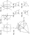
- FIGS. 6A to 6H are diagrams for explaining an example in which an image for a flat display is displayed on a curved display.
- display is corrected so that an image for a flat display is projected onto a curved display.
- Display is performed so that an image on a square flat plane S shown in FIG. 6A is projected onto a curved plane S′.
- display is performed so that the image is projected onto coordinates D(X, Y) on the curved plane S′.
- FIGS. 6A to 6H two axes on the flat plane S are the x-axis and the y-axis, and an axis toward the point C that is in the direction perpendicular to the flat plane S and serves as the viewpoint of the user is the z-axis.
- FIG. 6A shows overlap of the flat plane S and the curved plane S′ from the point C serving as the user's viewpoint, which can be represented by the xy coordinates.
- FIG. 6B shows the point C, the flat plane S, and the curved plane S′, which can be represented by the yz coordinates.
- FIG. 6C is a development diagram of the curved plane S′ to be represented by the xy coordinates.
- FIG. 6D shows the point C and a curved plane including an arc AG, an arc AL, an arc GL, an arc GF, and the like as part of the curved plane S′, which can be represented by the xyz coordinates.
- FIG. 6E shows a plane ACG excerpted from FIG. 6D .
- FIG. 6F shows a plane FCG excerpted from FIG. 6D .
- FIG. 6G shows a plane CLG excerpted from FIG. 6D .
- FIG. 6H shows a plane JMH excerpted from FIG. 6D .
- FIGS. 6A to 6H also show an angle ⁇ , an angle ⁇ , an angle ⁇ , and an angle ⁇ .
- X in the coordinates D(X, Y) is an arc DH and can be represented by Formula 1.
- r is a radius of curvature of the curved plane S′.
- the distance from the point C serving as the user's viewpoint to the flat plane S is also denoted by r.
- Step S 01 X and Y in D(X, Y) are given (Step S 01 ). Then, values of s and t are output using the lookup table 111 (Step S 02 ).
- data on the curvature radius r is contained as the shape data 106 stored in the memory circuit 107 .
- the lookup table 111 outputs the values of s and t by referring to the shape data 106 . The values of s and t are output as analog signals.
- the shape data 106 stored in the memory circuit 107 remains unchanged unless the shape of the curve surface included in the display is changed. For this reason, the values of s and t output from the lookup table 111 may be stored in a nonvolatile memory circuit. In this case, it is also possible to omit the memory circuit 107 while values including the shape data 106 to be stored in the memory circuit 107 are stored in the lookup table 111 instead.
- the exponentiation circuit 112 outputs s 2 t 2 and s 2 (Step S 03 ). Values of s 2 t 2 and s 2 are output as analog signals.
- An example of a circuit configuration of the exponentiation circuit 112 will be described later.
- the product-sum operation circuit 113 outputs (x 2 , y 2 ) (Step S 04 ). Values of (x 2 , y 2 ) are output as analog signals.
- An example of a circuit configuration of the product-sum operation circuit 113 will be described later.
- the square-root operation circuit 114 outputs (x, y) (Step S 05 ). Values of (x, y) are output as analog signals.
- An example of a circuit configuration of the square-root operation circuit 114 will be described later.
- Image data for the coordinates B(x, y) obtained from the above arithmetic operation is displayed at the coordinates D(X, Y), whereby an image for a flat surface can be projected onto a curved surface.
- the above configuration can also be applied to a display with a complicated shape.
- the exponentiation circuit 112 can obtain an intended arithmetic result by arithmetic processing of analog signals. This can make the power consumption and manufacturing cost unlikely to increase with an increasing amount of arithmetic operation when an arithmetic circuit for performing digital processing, such as a GPU or a CPU, is provided for each display to convert image data dedicated to displaying an image on a flat display into image data dedicated to displaying an image on a curved display.
- an arithmetic circuit for performing digital processing such as a GPU or a CPU
- FIG. 7A illustrates an example of a circuit capable of performing exponentiation operation in FIG. 5A .
- An exponentiation circuit illustrated in FIG. 7A includes a current supply circuit 121 and a transistor 122 .
- the exponentiation circuit in FIG. 7A is supplied with a power supply voltage VDD-GND.
- An analog voltage is applied to an input terminal IN, and the analog voltage obtained as a result of exponentiation operation is output from an output terminal OUT.
- the voltage of the output terminal OUT is determined by electrical characteristics of the transistor 122 .
- FIG. 7B illustrates an example of a circuit capable of performing square-root operation in FIG. 5A .
- the square-root operation circuit illustrated in FIG. 7B includes a transistor 131 , a transistor 132 , a transistor 133 , a transistor 134 , a transistor 135 , and a transistor 136 .
- the square-root operation circuit in FIG. 7B is supplied with the power supply voltage VDD-GND.
- the transistors 131 , 132 , and 133 are p-channel transistors
- the transistors 134 , 135 , and 136 are n-channel transistors.
- a voltage V BIAS is a voltage for supplying a constant current to the transistors 135 and 136 .
- An output current of a product-sum operation circuit is input to input terminals IN+ and IN ⁇ .
- a voltage of an output terminal OUT an output value in proportion to the half-power of the output current input to the input terminals IN+ and IN ⁇ is obtained.
- FIG. 8 illustrates a configuration example of a product-sum operation circuit.
- a product-sum operation circuit 10 illustrated in FIG. 8 includes a memory circuit 11 , a reference memory circuit 12 , a current source circuit 13 , a current sink circuit 14 , and a current supply circuit 15 .
- the memory circuit 11 includes memory cells MC such as a memory cell MC[i, j] and a memory cell MC[i+1, j].
- Each memory cell MC includes an element that has a function of converting an input potential into a current.
- an active element such as a transistor can be used, for example.
- FIG. 8 illustrates an example where each memory cell MC includes a transistor Tr 1 .
- a first analog potential is input to the memory cell MC through a wiring WD such as a wiring WD[j].
- the memory cell MC has a function of generating a first analog current corresponding to the first analog potential.
- the drain current of the transistor Tr 1 that is obtained when the first analog potential is supplied to a gate of the transistor Tr 1 can be used as the first analog current.
- a current flowing into the memory cell MC[i, j] is denoted by I[i, j]
- a current flowing into the memory cell MC[i+1, j] is denoted by I[i+1, j].
- the drain current of the transistor Tr 1 operating in a saturation region is not dependent on a voltage between its source and drain and is controlled by the difference between its gate voltage and threshold voltage.
- the transistor Tr 1 preferably operates in a saturation region.
- the gate voltage and the voltage between the source and drain of the transistor Tr 1 are assumed to be set within an appropriate range.
- a first analog potential Vx[i, j] or a potential corresponding to the first analog potential Vx[i, j] is input to the memory cell MC[i, j] through the wiring WD[j].
- the memory cell MC[i, j] has a function of generating a first analog current corresponding to the first analog potential Vx[i, j]. This means that here, the current I[i, j] in the memory cell MC[i, j] corresponds to the first analog current.
- a first analog potential Vx[i+1, j] or a potential corresponding to the first analog potential Vx[i+1, j] is input to the memory cell MC[i+1, j] through the wiring WD[j].
- the memory cell MC[i+1, j] has a function of generating a first analog current corresponding to the first analog potential Vx[i+1, j]. This means that here, the current I[i+1, j] in the memory cell MC[i+1, j] corresponds to the first analog current.
- the memory cell MC has a function of holding the first analog potential.
- the memory cell MC has a function of holding the first analog current corresponding to the first analog potential by holding the first analog potential.
- a second analog potential is input to the memory cell MC through a wiring RW such as a wiring RW[i] or a wiring RW[i+1].
- the memory cell MC has a function of adding the second analog potential or a potential corresponding to the second analog potential to the first analog potential that has been held, and a function of holding a third analog potential obtained by the addition.
- the memory cell MC also has a function of generating a second analog current corresponding to the third analog potential. In other words, the memory cell MC has a function of holding the second analog current corresponding to the third analog potential by holding the third analog potential.
- a second analog potential Vw[i, j] is input to the memory cell MC[i, j] through the wiring RW[i].
- the memory cell MC[i, j] has a function of holding a third analog potential corresponding to the first analog potential Vx[i, j] and the second analog potential Vw[i, j].
- the memory cell MC[i, j] also has a function of generating a second analog current corresponding to the third analog potential. This means that here, the current I[i, j] in the memory cell MC[i, j] corresponds to the second analog current.
- a second analog potential Vw[i+1, j] is input to the memory cell MC[i+1, j] through the wiring RW[i+1].
- the memory cell MC[i+1, j] has a function of holding a third analog potential corresponding to the first analog potential Vx[i+1, j] and the second analog potential Vw[i+1, j].
- the memory cell MC[i+1, j] also has a function of generating a second analog current corresponding to the third analog potential. This means that here, the current I[i+1, j] in the memory cell MC[i+1, j] corresponds to the second analog current.
- the current I[i, j] flows between a wiring BL[j] and a wiring VR[j] through the memory cell MC[i, j].
- the current I[i+1, j] flows between the wiring BL[j] and the wiring VR[j] through the memory cell MC[i+1, j].
- a current I[j] which corresponds to the sum of the current I[i, j] and the current I[i+1, j] flows between the wiring BL[j] and the wiring VR[j] through the memory cell MC[i, j] and the memory cell MC[i+1, j].
- the reference memory circuit 12 includes memory cells MCR such as a memory cell MCR[i] and a memory cell MCR[i+1].
- a first reference potential VPR is input to the memory cell MCR through a wiring WDREF.
- the memory cell MCR has a function of generating a first reference current corresponding to the first reference potential VPR.
- IREF[i] a current flowing into the memory cell MCR[i]
- IREF[i+1] a current flowing into the memory cell MCR[i+1]
- the first reference potential VPR is input to the memory cell MCR[i] through the wiring WDREF.
- the memory cell MCR[i] has a function of generating the first reference current corresponding to the first reference potential VPR. This means that here, the current IREF[i] in the memory cell MCR[i] corresponds to the first reference current.
- the first reference potential VPR is input to the memory cell MCR[i+1] through the wiring WDREF.
- the memory cell MCR[i+1] has a function of generating the first reference current corresponding to the first reference potential VPR. This means that here, the current IREF[i+1] in the memory cell MCR[i+1] corresponds to the first reference current.
- the memory cell MCR has a function of holding the first reference potential VPR.
- the memory cell MCR has a function of holding the first reference current corresponding to the first reference potential VPR by holding the first reference potential VPR.
- the second analog potential is input to the memory cell MCR through the wiring RW such as the wiring RW[i] or the wiring RW[i+1].
- the memory cell MCR has a function of adding the second analog potential or a potential corresponding to the second analog potential to the first reference potential VPR that has been held, and a function of holding a second reference potential obtained by the addition.
- the memory cell MCR also has a function of generating a second reference current corresponding to the second reference potential. In other words, the memory cell MCR has a function of holding the second reference current corresponding to the second reference potential by holding the second reference potential.
- the second analog potential Vw[i, j] is input to the memory cell MCR[i] through the wiring RW[i].
- the memory cell MCR[i] has a function of holding a second reference potential corresponding to the first reference potential VPR and the second analog potential Vw[i, j].
- the memory cell MCR[i] also has a function of generating a second reference current corresponding to the second reference potential. This means that here, the current IREF[i] in the memory cell MCR[i] corresponds to the second reference current.
- the second analog potential Vw[i+1, j] is input to the memory cell MCR[i+1] through the wiring RW[i+1].
- the memory cell MCR[i+1] has a function of holding a second reference potential corresponding to the first reference potential VPR and the second analog potential Vw[i+1, j].
- the memory cell MCR[i+1] also has a function of generating a second reference current corresponding to the second reference potential. This means that here, the current IREF[i+1] in the memory cell MCR[i+1] corresponds to the second reference current.
- the current IREF[i] flows between a wiring BLREF and a wiring VRREF through the memory cell MCR[i].
- the current IREF[i+1] flows between the wiring BLREF and the wiring VRREF through the memory cell MCR[i+1].
- a current IREF which corresponds to the sum of the current IREF[i] and the current IREF[i+1] flows between the wiring BLREF and the wiring VRREF through the memory cell MCR[i] and the memory cell MCR[i+1].
- the current supply circuit 15 has a function of supplying a current with the same value as the current IREF that flows through the wiring BLREF or supplying a current corresponding to the current IREF to a wiring BL.
- an offset current described later is set when the current I[j] that flows between the wiring BL[j] and the wiring VR[j] through the memory cell MC[i, j] and the memory cell MC[i+1, j] is different from the current IREF that flows between the wiring BLREF and the wiring VRREF through the memory cell MCR[i] and the memory cell MCR[i+1], a current corresponding to the difference flows to the current source circuit 13 or the current sink circuit 14 .
- the current source circuit 13 when the current I[j] is higher than the current IREF, the current source circuit 13 has a function of generating a current ⁇ I[j] that corresponds to the difference between the current I[j] and the current IREF.
- the current source circuit 13 also has a function of supplying the generated current ⁇ I[j] to the wiring BL[j]. This means that the current source circuit 13 has a function of holding the current ⁇ I[j].
- the current sink circuit 14 When the current I[j] is lower than the current IREF, the current sink circuit 14 has a function of generating the current ⁇ I[j], which corresponds to the difference between the current I[j] and the current IREF. The current sink circuit 14 also has a function of drawing the generated current ⁇ I[j] through the wiring BL[j]. This means that the current sink circuit 14 has a function of holding the current ⁇ I[j].
- a potential corresponding to the first analog potential is stored in the memory cell MC[i, j].
- a potential VPR ⁇ Vx[i, j] that is obtained by subtracting the first analog potential Vx[i, j] from the first reference potential VPR is input to the memory cell MC[i, j] through the wiring WD[j].
- the memory cell MC[i, j] holds the potential VPR ⁇ Vx[i, j].
- the memory cell MC[i, j] generates the current I[i, j] that corresponds to the potential VPR ⁇ Vx[i, j].
- the first reference potential VPR is a high-level potential that is higher than a ground potential.
- the first reference potential VPR is preferably higher than the ground potential and substantially the same as or lower than a high-level potential VDD that is supplied to the current supply circuit 15 .
- the first reference potential VPR is stored in the memory cell MCR[i]. Specifically, the potential VPR is input to the memory cell MCR[i] through the wiring WDREF. The memory cell MCR[i] holds the potential VPR. In addition, the memory cell MCR[i] generates the current IREF[i] that corresponds to the potential VPR.
- a potential corresponding to the first analog potential is stored in the memory cell MC[i+1, j].
- a potential VPR ⁇ Vx[i+1, j] that is obtained by subtracting the first analog potential Vx[i+1, j] from the first reference potential VPR is input to the memory cell MC[i+1, j] through the wiring WD[j].
- the memory cell MC[i+1, j] holds the potential VPR ⁇ Vx[i+1, j].
- the memory cell MC[i+1, j] generates the current I[i+1, j] that corresponds to the potential VPR ⁇ Vx[i+1, j].
- the first reference potential VPR is stored in the memory cell MCR[i+1]. Specifically, the potential VPR is input to the memory cell MCR[i+1] through the wiring WDREF. The memory cell MCR[i+1] holds the potential VPR. In addition, the memory cell MCR[i+1] generates the current IREF[i+1] that corresponds to the potential VPR.
- the wiring RW[i] and the wiring RW[i+1] are set to a standard potential.
- the standard potential include the ground potential and a low-level potential VSS that is lower than the ground potential.
- the standard potential can be a potential between the potential VSS and the potential VDD. This is preferable because the potential of the wiring RW can be higher than the ground potential regardless of whether the second analog potential Vw is positive or negative, which enables easy generation of signals and multiplication of positive and negative potentials.
- a current corresponding to the sum of currents generated in the memory cells MC connected to the wiring BL[j] flows through the wiring BL[j].
- the current I[j] which is the sum of the current I[i, j] generated in the memory cell MC[i, j] and the current I[i+1, j] generated in the memory cell MC[i+1, j] flows through the wiring BL[j].
- a current corresponding to the sum of currents generated in the memory cells MCR connected to the wiring BLREF flows through the wiring BLREF.
- the current IREF which is the sum of the current IREF[i] generated in the memory cell MCR[i] and the current IREF[i+1] generated in the memory cell MCR[i+1] flows through the wiring BLREF.
- an offset current Ioffset[j] that is the difference between the current I[j] obtained by inputting the first analog potential and the current IREF obtained by inputting the first reference potential is held in the current source circuit 13 or the current sink circuit 14 while the wiring RW[i] and the wiring RW[i+1] are kept at the standard potential.
- the current source circuit 13 supplies the current Ioffset[j] to the wiring BL[j]. This means that a current ICM[j] that flows into the current source circuit 13 corresponds to the current Ioffset[j]. The value of the current ICM[j] is held in the current source circuit 13 .
- the current sink circuit 14 draws the current Ioffset[j] through the wiring BL[j]. This means that a current ICP[j] that flows into the current sink circuit 14 corresponds to the current Ioffset[j]. The value of the current ICP[j] is held in the current sink circuit 14 .
- the second analog potential or a potential corresponding to the second analog potential is stored in the memory cell MC[i, j] so as to be added to the first analog potential or a potential corresponding to the first analog potential that has been held in the memory cell MC[i, j].
- the potential of the wiring RW[i] is set higher than the standard potential by Vw[i], whereby a second analog potential Vw[i] is input to the memory cell MC[i, j] through the wiring RW[i].
- the memory cell MC[i, j] holds a potential VPR ⁇ Vx[i, j]+Vw[i].
- the memory cell MC[i, j] generates the current I[i, j] corresponding to the potential VPR ⁇ Vx[i, j]+Vw[i].
- the second analog potential or a potential corresponding to the second analog potential is stored in the memory cell MC[i+1, j] so as to be added to the first analog potential or a potential corresponding to the first analog potential that has been held in the memory cell MC[i+1, j].
- the potential of the wiring RW[i+1] is set higher than the standard potential by Vw[i+1], whereby a second analog potential Vw[i+1] is input to the memory cell MC[i+1, j] through the wiring RW[i+1].
- the memory cell MC[i+1, j] holds a potential VPR ⁇ Vx[i+1, j]+Vw[i+1].
- the memory cell MC[i+1, j] generates the current I[i+1, j] corresponding to the potential VPR ⁇ Vx[i+1, j]+Vw[i+1].
- the drain current of the transistor Tr 1 included in the memory cell MC[i, j] corresponds to the current I[i, j].
- the second analog current is expressed by the following Formula 10, given that the potential of the wiring RW[i] is Vw[i] and the potential of the wiring RW[i+1] is Vw[i+1].
- k is a coefficient
- Vth is the threshold voltage of the transistor Tr 1 .
- the current I[j] which corresponds to the sum of the current I[i, j] flowing into the memory cell MC[i, j] and the current I[i+1, j] flowing into the memory cell MC[i+1, j] is expressed as ⁇ iI[i, j].
- the current IREF which corresponds to the sum of the current IREF[i] flowing into the memory cell MCR[i] and the current IREF[i+1] flowing into the memory cell MCR[i+1] flowing into the memory cell MCR[i+1]
- ⁇ iIREF[i] Accordingly, the current ⁇ I[j] that corresponds to the difference between the current I[j] and the current IREF is expressed by Formula 12.
- a current Iout[j] that flows from the wiring BL[j] is expressed by IREF ⁇ I[j] ⁇ Ioffset[j], where I[j] is the sum of currents flowing into the memory cells MC, IREF is the sum of currents flowing into the memory cells MCR, and Ioffset[j] is a current flowing into the current source circuit 13 or the current sink circuit 14 .
- the current Iout[j] equals to 2k ⁇ i(Vw[i] ⁇ Vx[i, j]), which corresponds to the sum of the product of the first analog potential Vx[i, j] and the second analog potential Vw[i] and the product of the first analog potential Vx[i+1, j] and the second analog potential Vw[i+1].
- the transistor Tr 1 preferably operates in a saturation region. However, even if the operation region of the transistor Tr 1 deviates from an ideal saturation region, the transistor Tr 1 is regarded as operating in a saturation region as long as there is no problem in obtaining a current that corresponds to the sum of the product of the first analog potential Vx[i, j] and the second analog potential Vw[i] and the product of the first analog potential Vx[i+1, j] and the second analog potential Vw[i+1] with an accuracy within a desired range.
- the product-sum operation circuit can perform arithmetic processing on analog data without converting analog data into digital data; thus, the circuit scale of a semiconductor device can be reduced or the time required for the arithmetic processing of analog data can be shortened.
- power consumption of a semiconductor device can be reduced while the time required for arithmetic processing of analog data is shortened.
- FIG. 9 shows an example of a specific circuit configuration of memory cells MC in given two rows and two columns and memory cells MCR in given two rows and one column, and a connection relation between these memory cells.
- FIG. 9 illustrates the memory cell MC[i, j] in the i-th row and the j-th column, the memory cell MC[i+1, j] in the (i+1)th row and the j-th column, a memory cell MC[i, j+1] in the i-th row and the (j+1)th column, and a memory cell MC[i+1, j+1] in the (i+1)th row and the (j+1)th column.
- FIG. 9 also illustrates the memory cell MCR[i] in the i-th row and the memory cell MCR[i+1] in the (i+1)th row.
- the memory cell MC[i, j], the memory cell MC[i, j+1], and the memory cell MCR[i] in the i-th row are connected to the wiring RW[i] and a wiring WW[i].
- the memory cell MC[i+1, j], the memory cell MC[i+1, j+1], and the memory cell MCR[i+1] in the (i+1)th row are connected to the wiring RW[i+1] and a wiring WW[i+1].
- the memory cell MC[i, j] and the memory cell MC[i+1, j] in the j-th column are connected to the wiring WD[j], the wiring VR[j], and the wiring BL[j].
- the memory cell MC[i, j+1] and the memory cell MC[i+1, j+1] in the (j+1)th column are connected to a wiring WD[j+1], a wiring VR[j+1], and a wiring BL[j+1].
- the memory cell MCR[i] in the i-th row and the memory cell MCR[i+1] in the (i+1)th row are connected to the wiring WDREF, the wiring VRREF, and the wiring BLREF.
- the memory cells MC and MCR each include the transistor Tr 1 , a transistor Tr 2 , and a capacitor C 1 .
- the transistor Tr 2 has a function of controlling the input of the first analog potential to the memory cell MC or the memory cell MCR.
- the transistor Tr 1 has a function of generating an analog current in accordance with a potential input to its gate.
- the capacitor C 1 has a function of adding the second analog potential or a potential corresponding to the second analog potential to the first analog potential or a potential corresponding to the first analog potential that is held in the memory cell MC or the memory cell MCR.
- a gate of the transistor Tr 2 is connected to the wiring WW
- one of a source and a drain of the transistor Tr 2 is connected to the wiring WD
- the other of the source and the drain of the transistor Tr 2 is connected to the gate of the transistor Tr 1 .
- One of a source and a drain of the transistor Tr 1 is connected to the wiring VR, and the other of the source and the drain of the transistor Tr 1 connected to the wiring BL.
- a first electrode of the capacitor C 1 is connected to the wiring RW, and a second electrode of the capacitor C 1 is connected to the gate of the transistor Tr 1 .
- the gate of the transistor Tr 2 is connected to the wiring WW
- one of the source and the drain of the transistor Tr 2 is connected to the wiring WDREF
- the other of the source and the drain of the transistor Tr 2 is connected to the gate of the transistor Tr 1 .
- One of the source and the drain of the transistor Tr 1 is connected to the wiring VRREF
- the other of the source and the drain of the transistor Tr 1 is connected to the wiring BLREF.
- the first electrode of the capacitor C 1 is connected to the wiring RW
- the second electrode of the capacitor C 1 is connected to the gate of the transistor Tr 1 .
- the gate of the transistor Tr 1 in the memory cell MC is referred to as a node N here.
- the first analog potential or a potential corresponding to the first analog potential is input to the node N through the transistor Tr 2 .
- the transistor Tr 2 is turned off, the node N is brought into a floating state and the first analog potential or the potential corresponding to the first analog potential is held at the node N.
- the second analog potential or a potential corresponding to the second analog potential that is input to the first electrode of the capacitor C 1 is supplied to the node N.
- the node N can have a potential obtained by adding the second analog potential or the potential corresponding to the second analog potential to the first analog potential or the potential corresponding to the first analog potential.
- the amount of change in the potential of the node N is not exactly the same as the amount of change in the potential of the first electrode in an actual circuit.
- the accurate amount of change in the potential of the node N can be calculated in the following manner: a coupling coefficient that is uniquely determined by the capacitance of the capacitor C 1 , the gate capacitance of the transistor Tr 1 , and a parasitic capacitance is multiplied by the amount of change in the potential of the first electrode.
- the amount of change in the potential of the node N is assumed to be substantially the same as the amount of change in the potential of the first electrode.
- the drain current of the transistor Tr 1 is determined in accordance with the potential of the node N. Thus, when the transistor Tr 2 is turned off, the value of the drain current of the transistor Tr 1 as well as the potential of the node N is held. The drain current is affected by the first analog potential and the second analog potential.
- the gate of the transistor Tr 1 in the memory cell MCR is referred to as a node NREF here.
- the first reference potential or a potential corresponding to the first reference potential is input to the node NREF through the transistor Tr 2 .
- the transistor Tr 2 is turned off, the node NREF is brought into a floating state and the first reference potential or the potential corresponding to the first reference potential is held at the node NREF.
- the node NREF when the node NREF is brought into a floating state, the second analog potential or a potential corresponding to the second analog potential that is input to the first electrode of the capacitor C 1 is supplied to the node NREF.
- the node NREF can have a potential obtained by adding the second analog potential or the potential corresponding to the second analog potential to the first reference potential or the potential corresponding to the first reference potential.
- the drain current of the transistor Tr 1 is determined in accordance with the potential of the node NREF. Thus, when the transistor Tr 2 is turned off, the value the drain current of the transistor Tr 1 as well as the potential of the node NREF is held. The drain current is affected by the first reference potential and the second analog potential.
- the drain current of the transistor Tr 1 in the memory cell MC[i, j] is the current I[i, j] and the drain current of the transistor Tr 1 in the memory cell MC[i+1, j] is the current I[i+1, j]
- the sum of currents supplied to the memory cell MC[i, j] and the memory cell MC[i+1, j] through the wiring BL[j] is the current I[j].
- the drain current of the transistor Tr 1 in the memory cell MC[i, j+1] is a current I[i, j+1] and the drain current of the transistor Tr 1 in the memory cell MC[i+1, j+1] is a current I[i+1, j+1]
- the sum of currents supplied to the memory cell MC[i, j+1] and the memory cell MC[i+1, j+1] through the wiring BL[j+1] is a current I[j+1].
- the drain current of the transistor Tr 1 in the memory cell MCR[i] is the current IREF[i] and the drain current of the transistor Tr 1 in the memory cell MCR[i+1] is the current IREF[i+1]
- the sum of currents supplied to the memory cell MCR[i] and the memory cell MCR[i+1] through the wiring BLREF is the current IREF.
- the current source circuit 13 illustrated in FIG. 9 includes a current source circuit 13 [ j ] for the memory cells MC in the j-th column and a current source circuit 13 [ j+ 1] for the memory cells MC in the (j+1)th column.
- the current sink circuit 14 illustrated in FIG. 9 includes a current sink circuit 14 [ j ] for the memory cells MC in the j-th column and a current sink circuit 14 [ j+ 1] for the memory cells MC in the (j+1)th column.
- the current source circuit 13 [ j ] and the current sink circuit 14 [ j ] are connected to the wiring BL[j].
- the current source circuit 13 [ j+ 1] and the current sink circuit 14 [ j+ 1] are connected to the wiring BL[j+1].
- the current supply circuit 15 is connected to the wiring BL[j], the wiring BL[j+1], and the wiring BLREF.
- the current supply circuit 15 has a function of supplying the current IREF to the wiring BLREF, and a function of supplying a current that is the same as the current IREF or a current that corresponds to the current IREF to each of the wiring BL[j] and the wiring BL[j+1].
- the current source circuit 13 [ j ] and the current source circuit 13 [ j+ 1] each include a transistor Tr 7 , a transistor Tr 8 , a transistor Tr 9 , and a capacitor C 3 .
- the transistor Tr 7 in the current source circuit 13 [ j ] has a function of generating the current ICM[j] that corresponds to the difference between the current I[j] and the current IREF, when the current I[j] is higher than the current IREF;
- the transistor Tr 7 in the current source circuit 13 [ j+ 1] has a function of generating a current ICM[j+1] that corresponds to the difference between the current I[j+1] and the current IREF, when the current I[j+1] is higher than the current IREF.
- the current ICM[j] and the current ICM[j+1] are supplied from the current source circuit 13 [ j ] and the current source circuit 13 [ j+ 1] to the wiring BL[j] and the wiring BL[
- each of the current source circuit 13 [ j ] and the current source circuit 13 [ j+ 1] one of a source and a drain of the transistor Tr 7 is connected to the wiring BL, and the other of the source and the drain is connected to a wiring supplied with a predetermined potential.
- One of a source and a drain of the transistor Tr 8 is connected to the wiring BL, and the other of the source and the drain is connected to a gate of the transistor Tr 7 .
- One of a source and a drain of the transistor Tr 9 is connected to the gate of the transistor Tr 7 , and the other of the source and the drain is connected to a wiring supplied with a predetermined potential.
- a first electrode of the capacitor C 3 is connected to the gate of the transistor Tr 7 , and a second electrode of the capacitor C 3 is connected to a wiring supplied with a predetermined potential.
- a gate of the transistor Tr 8 is connected to a wiring OSM, and a gate of the transistor Tr 9 is connected to a wiring ORM.
- FIG. 9 illustrates an example where the transistor Tr 7 is a p-channel transistor and the transistors Tr 8 and Tr 9 are n-channel transistors.
- the current sink circuit 14 [ j ] and the current sink circuit 14 [ j+ 1] each include a transistor Tr 4 , a transistor Try, a transistor Tr 6 , and a capacitor C 4 .
- the transistor Tr 4 in the current sink circuit 14 [ j ] has a function of generating the current ICP[j] that corresponds to the difference between the current I[j] and the current IREF, when the current I[j] is lower than the current IREF;
- the transistor Tr 4 in the current sink circuit 14 [ j+ 1] has a function of generating a current ICP[j+1] that corresponds to the difference between the current I[j+1] and the current IREF, when the current I[j+1] is lower than the current IREF.
- the current ICP[j] and the current ICP[j+1] are drawn from the wiring BL[j] and the wiring BL[j+1] into the current sink circuit 14 [ j ] and the current sink circuit 14 [ j+ 1], respectively.
- each of the current sink circuit 14 [ j ] and the current sink circuit 14 [ j+ 1] one of a source and a drain of the transistor Tr 4 is connected to the wiring BL, and the other of the source and the drain is connected to a wiring supplied with a predetermined potential.
- One of a source and a drain of the transistor Tr 5 is connected to the wiring BL, and the other of the source and the drain is connected to a gate of the transistor Tr 4 .
- One of a source and a drain of the transistor Tr 6 is connected to the gate of the transistor Tr 4 , and the other of the source and the drain is connected to a wiring supplied with a predetermined potential.
- a first electrode of the capacitor C 4 is connected to the gate of the transistor Tr 4 , and a second electrode of the capacitor C 4 is connected to a wiring supplied with a predetermined potential.
- a gate of the transistor Tr 5 is connected to a wiring OSP, and a gate of the transistor Tr 6 is connected to a wiring ORP.
- FIG. 9 illustrates an example where the transistors Tr 4 to Tr 6 are n-channel transistors.
- the current supply circuit 15 includes a transistor Tr 10 for the wiring BL and a transistor Tr 11 for the wiring BLREF.
- FIG. 9 illustrates an example where the current supply circuit 15 includes, as the transistor Tr 10 , a transistor Tr 10 [ j ] for the wiring BL[j] and a transistor Tr 10 [ j+ 1] for the wiring BL[j+1].
- a gate of the transistor Tr 10 is connected to a gate of the transistor Tr 11 .
- One of a source and a drain of the transistor Tr 10 is connected to the wiring BL, and the other of the source and the drain is connected to a wiring supplied with a predetermined potential.
- One of a source and a drain of the transistor Tr 11 is connected to the wiring BLREF, and the other of the source and the drain is connected to a wiring supplied with a predetermined potential.
- the transistors Tr 10 and Tr 11 have the same polarity.
- FIG. 9 shows an example where the transistors Tr 10 and Tr 11 are p-channel transistors.
- the drain current of the transistor Tr 11 corresponds to the current IREF.
- the transistor Tr 10 and the transistor Tr 11 collectively function as a current mirror circuit; thus, the drain current of the transistor Tr 10 is substantially the same as the drain current of the transistor Tr 11 or corresponds to the drain current of the transistor Tr 11 .
- FIG. 10 is an example of a timing chart showing the operation of the memory cells MC, the memory cells MCR, the current source circuit 13 , the current sink circuit 14 , and the current supply circuit 15 illustrated in FIG. 9 .
- the first analog current is stored in the memory cells MC and the memory cells MCR.
- the value of the offset current Ioffset that is supplied from the current source circuit 13 and the current sink circuit 14 is set.
- Time T 11 to Time T 16 data corresponding to the product-sum of the first analog current and the second analog current is acquired.
- a low-level potential is supplied to the wiring VR[j] and the wiring VR[j+1].
- the high-level potential VDD is supplied to all wirings having a predetermined potential that are connected to the current source circuit 13 .
- the low-level potential VSS is supplied to all wirings having a predetermined potential that are connected to the current sink circuit 14 .
- the high-level potential VDD is supplied to all wirings having a predetermined potential that are connected to the current supply circuit 15 .
- Each of the transistors Tr 1 , Tr 4 , Tr 7 , Tr 10 [ j ], Tr 10 [ j+ 1], and Tr 11 operates in a saturation region.
- a high-level potential is supplied to the wiring WW[i] and a low-level potential is supplied to the wiring WW[i+1]. Accordingly, the transistors Tr 2 in the memory cell MC[i, j], the memory cell MC[i, j+1], and the memory cell MCR[i] illustrated in FIG. 9 are turned on. The transistors Tr 2 in the memory cell MC[i+1, j], the memory cell MC[i+1, j+1], and the memory cell MCR[i+1] remain off.
- a potential obtained by subtracting the first analog potential from the first reference potential VPR is supplied to each of the wiring WD[j] and the wiring WD[j+1] in FIG. 9 .
- the potential VPR ⁇ Vx[i, j] is supplied to the wiring WD[j]
- a potential VPR ⁇ Vx[i, j+1] is supplied to the wiring WD[j+1].
- the first reference potential VPR is supplied to the wiring WDREF, and a potential between the potential VSS and the potential VDD, e.g., a potential (VDD+VSS)/2, is supplied as the standard potential to the wiring RW[i] and the wiring RW[i+1].
- the potential VPR ⁇ Vx[i, j] is supplied to a node N[i, j] through the transistor Tr 2 in the memory cell MC[i, j] illustrated in FIG. 9
- the potential VPR ⁇ Vx[i, j+1] is supplied to a node N[i, j+1] through the transistor Tr 2 in the memory cell MC[i, j+1]
- the potential VPR is supplied to a node NREF[i] through the transistor Tr 2 in the memory cell MCR[i].
- the potential supplied to the wiring WW[i] illustrated in FIG. 9 changes from a high-level potential to a low-level potential, so that the transistors Tr 2 in the memory cell MC[i, j], the memory cell MC[i, j+1], and the memory cell MCR[i] are turned off. Accordingly, the potential VPR ⁇ Vx[i, j] is held at the node N[i, j], the potential VPR ⁇ Vx[i, j+1] is held at the node N[i, j+1], and the potential VPR is held at the node NREF[i].
- the potential of the wiring WW[i] illustrated in FIG. 9 remains at a low level and a high-level potential is supplied to the wiring WW[i+1]. Accordingly, the transistors Tr 2 in the memory cell MC[i+1, j], the memory cell MC[i+1, j+1], and the memory cell MCR[i+1] illustrated in FIG. 9 are turned on. The transistors Tr 2 in the memory cell MC[i, j], the memory cell MC[i, j+1], and the memory cell MCR[i] remain off.
- a potential obtained by subtracting the first analog potential from the first reference potential VPR is supplied to each of the wiring WD[j] and the wiring WD[j+1] illustrated in FIG. 9 .
- the potential VPR ⁇ Vx[i+1, j] is supplied to the wiring WD[j]
- a potential VPR ⁇ Vx[i+1, j+1] is supplied to the wiring WD[j+1].
- the first reference potential VPR is supplied to the wiring WDREF, and a potential between the potential VSS and the potential VDD, e.g., the potential (VDD+VSS)/2, is supplied as the standard potential to the wiring RW[i] and the wiring RW[i+1].
- the potential VPR ⁇ Vx[i+1, j] is supplied to a node N[i+1, j] through the transistor Tr 2 in the memory cell MC[i+1, j] illustrated in FIG. 9
- the potential VPR ⁇ Vx[i+1, j+1] is supplied to a node N[i+1, j+1] through the transistor Tr 2 in the memory cell MC[i+1, j+1]
- the potential VPR is supplied to a node NREF[i+1] through the transistor Tr 2 in the memory cell MCR[i+1].
- the potential supplied to the wiring WW[i+1] in FIG. 9 changes from a high-level potential to a low-level potential, so that the transistors Tr 2 in the memory cell MC[i+1, j], the memory cell MC[i+1, j+1], and the memory cell MCR[i+1] are turned off. Accordingly, the potential VPR ⁇ Vx[i+1, j] is held at the node N[i+1, j], the potential VPR ⁇ Vx[i+1, j+1] is held at the node N[i+1, j+1], and the potential VPR is held at the node NREF[i+1].
- a high-level potential is supplied to the wiring ORP and the wiring ORM illustrated in FIG. 9 .
- the transistors Tr 9 in the current source circuit 13 [ j ] and the current source circuit 13 [ j+ 1] in FIG. 9 are turned on, so that the gates of the transistors Tr 7 are reset by the potential VDD supplied thereto.
- the transistors Tr 6 in the current sink circuit 14 [ j ] and the current sink circuit 14 [ j+ 1] in FIG. 9 are turned on, so that the gates of the transistors Tr 4 are reset by the potential VSS supplied thereto.
- the potentials supplied to the wiring ORP and the wiring ORM illustrated in FIG. 9 change from a high-level potential to a low-level potential, so that the transistors Tr 9 in the current source circuit 13 [ j ] and the current source circuit 13 [ j+ 1] and the transistors Tr 6 in the current sink circuit 14 [ j ] and the current sink circuit 14 [ j+ 1] are turned off. Accordingly, the potential VDD is held at the gates of the transistors Tr 7 in the current source circuit 13 [ j ] and the current source circuit 13 [ j+ 1], and the potential VSS is held at the gates of the transistors Tr 4 in the current sink circuit 14 [ j ] and the current sink circuit 14 [ j+ 1].
- a high-level potential is supplied to the wiring OSP illustrated in FIG. 9 .
- a potential between the potential VSS and the potential VDD e.g., the potential (VDD+VSS)/2, is supplied as the standard potential to each of the wiring RW[i] and the wiring RW[i+1] illustrated in FIG. 9 .
- the transistors Tr 5 in the current sink circuit 14 [ j ] and the current sink circuit 14 [ j+ 1] are turned on.
- the current ⁇ I[j] has a positive value
- part of the drain current of the transistor Tr 10 [ j ] flows to the gate of the transistor Tr 4 when the transistor Tr 5 is turned on in the current sink circuit 14 [ j ], and the potential of the gate of the transistor Tr 4 starts to rise.
- the potential of the gate of the transistor Tr 4 converges on a certain value.
- the transistor Tr 4 in the current sink circuit 14 [ j+ 1] is in a state of serving as a current supply that can supply the current ICP[j+1].
- the potential supplied to the wiring OSP in FIG. 9 changes from a high-level potential to a low-level potential, so that the transistors Tr 5 in the current sink circuit 14 [ j ] and the current sink circuit 14 [ j+ 1] are turned off. Accordingly, the potentials of the gates of the transistors Tr 4 are held.
- the current sink circuit 14 [ j ] remains in a state of serving as the current supply that can supply the current ICP[j]
- the current sink circuit 14 [ j+ 1] remains in a state of serving as the current supply that can supply the current ICP[j+1].
- a high-level potential is supplied to the wiring OSM in FIG. 9 .
- a potential between the potential VSS and the potential VDD e.g., the potential (VDD+VSS)/2, is supplied as the standard potential to each of the wiring RW[i] and the wiring RW[i+1] in FIG. 9 .
- the transistors Tr 8 in the current source circuit 13 [ j ] and the current source circuit 13 [ j+ 1] are turned on.
- the current ⁇ I[j] has a negative value
- a current flows from the gate of the transistor Tr 7 to the wiring BL[j] when the transistor Tr 8 is turned on in the current source circuit 13 [ j ], and the potential of the gate of the transistor Tr 7 starts to decrease.
- the potential of the gate of the transistor Tr 7 converges on a certain value.
- the transistor Tr 7 in the current source circuit 13 [ j+ 1] is in a state of serving as a current supply that can supply the current ICM[j+1].
- the potential supplied to the wiring OSM in FIG. 9 changes from a high-level potential to a low-level potential, so that the transistors Tr 8 in the current source circuit 13 [ j ] and the current source circuit 13 [ j+ 1] are turned off. Accordingly, the potentials of the gates of the transistors Tr 7 are held.
- the current source circuit 13 [ j ] remains in a state of serving as the current supply that can supply the current ICM[j]
- the current source circuit 13 [ j+ 1] remains in a state of serving as the current supply that can supply the current ICM[j+1].
- the transistor Tr 4 has a function of drawing a current.
- the transistor Tr 4 has a function of drawing a current.
- the transistor Tr 1 in the memory cell MC it might be difficult for the transistor Tr 1 in the memory cell MC, the transistor Tr 4 in the current sink circuit 14 [ j ] or the current sink circuit 14 [ j+ 1], and the transistor Tr 10 [ j ] or the transistor Tr 10 [ j+ 1] to concurrently operate in a saturation region because a balance is struck between the current flowing through the wiring BLREF and the current flowing through the wiring BL[j] or the wiring BL[j+1].
- the potential of the gate of the transistor Tr 7 may be set to a potential that is high enough to obtain a predetermined drain current, instead of resetting the potential of the gate of the transistor Tr 7 to the potential VDD, from Time T 05 to Time T 06 .
- the amount of current that cannot be drawn by the transistor Tr 1 can be drawn by the transistor Tr 4 to some extent because a current from the transistor Tr 7 , as well as the drain current of the transistor Tr 10 [ j ] or the transistor Tr 10 [ j+ 1], is supplied.
- the operation of the transistor Tr 1 , the transistor Tr 4 , and the transistor Tr 10 [ j ] or the transistor Tr 10 [ j+ 1] in a saturation region can be ensured.
- the second analog potential Vw[i] is supplied to the wiring RW[i] illustrated in FIG. 9 .
- a potential between the potential VSS and the potential VDD e.g., the potential (VDD+VSS)/2
- VDD+VSS the potential between the potential VSS and the potential VDD
- Vw[i] the potential of the wiring RW[i] is assumed to be the potential Vw[i].
- the product-sum of the first analog current and the second analog current for the memory cell MC[i, j] affects a current obtained by subtracting the current Ioffset[j] from the current ⁇ I[j], that is, the current Iout[j] flowing from the wiring BL[j].
- the product-sum of the first analog current and the second analog current for the memory cell MC[i, j+1] affects a current obtained by subtracting the current Ioffset[j+1] from the current ⁇ I[j+1], that is, a current Iout[j+1] flowing from the wiring BL[j+1].
- a potential between the potential VSS and the potential VDD (e.g., the potential (VDD+VSS)/2), which is the standard potential, is supplied again to the wiring RW[i].
- the second analog potential Vw[i+1] is supplied to the wiring RW[i+1] illustrated in FIG. 9 .
- a potential between the potential VSS and the potential VDD e.g., the potential (VDD+VSS)/2
- VDD+VSS the potential between the potential VSS and the potential VDD
- the potential of the wiring RW[i+1] is assumed to be the potential Vw[i+1].
- the product-sum of the first analog current and the second analog current for the memory cell MC[i+1, j] affects a current obtained by subtracting the current Ioffset[j] from the current ⁇ I[j], that is, the current Iout[j]. Furthermore, the product-sum of the first analog current and the second analog current for the memory cell MC[i, j+1] and the memory cell MC[i+1, j+1] affects a current obtained by subtracting the current Ioffset[j+1] from the current ⁇ I[j+1], that is, the current Iout[j+1].
- a potential between the potential VSS and the potential VDD (e.g., the potential (VDD+VSS)/2), which is the standard potential, is supplied again to the wiring RW[i+1].
- the second analog potential Vw[i] is supplied to the wiring RW[i] in FIG. 9 and the second analog potential Vw[i+1] is supplied to the wiring RW[i+1].
- the potential of the wiring RW[i] is a potential higher than the potential between the potential VSS and the potential VDD (e.g., the potential (VDD+VSS)/2), which is the standard potential, by Vw[i] and the potential of the wiring RW[i+1] is a potential higher than the potential between the potential VSS and the potential VDD (e.g., the potential (VDD+VSS)/2) by Vw[i+1].
- the potential of the wiring RW[i] is assumed to be the potential Vw[i] and the potential of the wiring RW[i+1] is assumed to be the potential Vw[i+1].
- the product-sum of the first analog current and the second analog current for the memory cell MC[i, j] and the memory cell MC[i+1, j] affects a current obtained by subtracting the current Ioffset[j] from the current ⁇ I[j], that is, the current Iout[j]. Furthermore, the product-sum of the first analog current and the second analog current for the memory cell MC[i, j+1] and the memory cell MC[i+1, j+1] affects a current obtained by subtracting the current Ioffset[j+1] from the current ⁇ I[j+1], that is, the current Iout[j+1].
- a potential between the potential VSS and the potential VDD (e.g., the potential (VDD+VSS)/2), which is the standard potential, is supplied again to the wiring RW[i] and the wiring RW[i+1].
- the product-sum operation can be performed with a small-scale circuit, at high speed, and/or with low power consumption.
- a transistor with an extremely low off-state current is preferably used as the transistor Tr 2 , Tr 5 , Tr 6 , Tr 8 , or Tr 9 .
- the transistor Tr 2 the potential of the node N can be held for a long time.
- a transistor with an extremely low off-state current is used as the transistors Tr 5 and Tr 6 , the potential of the gate of the transistor Tr 4 can be held for a long time.
- a transistor with an extremely low off-state current is used as the transistors Tr 8 and Tr 9 , the potential of the gate of the transistor Tr 7 can be held for a long time.
- a channel formation region contains a semiconductor with a wide energy gap, for example.
- the energy gap of the semiconductor is preferably greater than or equal to 2.5 eV, greater than or equal to 2.7 eV, or greater than or equal to 3 eV.
- An example of such a semiconductor material is an oxide semiconductor.
- a transistor containing an oxide semiconductor in a channel formation region can be used as the transistor Tr 2 , Tr 5 , Tr 6 , Tr 8 , or Tr 9 .
- the leakage current of an OS transistor normalized by channel width can be lower than or equal to 10 ⁇ 10 ⁇ 21 A/ ⁇ m (10 zA/ ⁇ m) with a source-drain voltage of 10 V at room temperature (approximately 25° C.).
- the leakage current of an OS transistor used as the transistor Tr 2 , Tr 5 , Tr 6 , Tr 8 , or Tr 9 is preferably lower than or equal to 1 ⁇ 10 ⁇ 18 A, lower than or equal to 1 ⁇ 10 ⁇ 21 A, or lower than or equal to 1 ⁇ 10 ⁇ 24 A at room temperature (approximately 25° C.).
- the leakage current is preferably lower than or equal to 1 ⁇ 10 ⁇ 15 A, lower than or equal to 1 ⁇ 10 ⁇ 18 A, or lower than or equal to 1 ⁇ 10 ⁇ 21 A at 85° C.
- An oxide semiconductor is a wide energy gap semiconductor in which electrons are unlikely to be excited and the effective mass of a hole is large. Accordingly, an avalanche breakdown and the like are less likely to occur in an OS transistor than in a typical transistor using silicon or the like. Since hot-carrier degradation or the like due to the avalanche breakdown is inhibited, an OS transistor has high drain withstand voltage and can be driven at high drain voltage.
- An oxide semiconductor contained in a channel formation region of a transistor is preferably an oxide semiconductor containing at least one of indium (In) and zinc (Zn).
- oxide semiconductor include In oxide, Zn oxide, In—Zn oxide, and In—M—Zn oxide (M is Ga, Al, Ti, Y, Zr, La, Ce, Nd, or Hf).
- Reduction in impurities serving as electron donors, such as hydrogen, and reduction in oxygen vacancies can make an oxide semiconductor an i-type (intrinsic) or substantially i-type semiconductor.
- Such an oxide semiconductor can be referred to as a highly purified oxide semiconductor.
- An oxide semiconductor with a low carrier density is preferably used for a channel formation region.
- the carrier density of the oxide semiconductor is preferably less than 8 ⁇ 10 11 /cm 3 and greater than or equal to 1 ⁇ 10 ⁇ 9 /cm 3 .
- the carrier density is further preferably less than 1 ⁇ 10 11 /cm 3 , still further preferably less than 1 ⁇ 10 10 /cm 3 .
- FIG. 11A is a block diagram of a structure example of the memory circuit 107 .
- the block diagram in FIG. 11A illustrates a memory cell array 90 , a word line driver circuit 91 , and a bit line driver circuit 92 .
- the memory cell array 90 includes memory cells MC arranged in a matrix of m rows and n columns (m and n are each a natural number).
- the memory cells MC are connected to word lines WL_ 1 to WL_m and bit lines BL_ 1 to BL_n.
- the memory cells MC may be connected to a source line for supplying current, a wiring for applying voltage to a backgate of a transistor, a capacitor line for fixing a potential of one electrode of a capacitor, or the like.
- the word line driver circuit 91 is a circuit that outputs a signal for selecting the memory cells MC in each row. Word lines for data writing and word lines for data reading may be provided separately as the word lines WL_ 1 to WL_m.
- the bit line driver circuit 92 is a circuit for writing data into the memory cells MC in each column or for reading data from the memory cells MC. Bit lines for data writing and bit lines for data reading may be provided separately as the bit lines BL_ 1 to BL_n.
- FIGS. 11B to 11F illustrate examples of a circuit configuration that the memory cell MC in FIG. 11A can have.
- a memory cell MC_A illustrated in FIG. 11B includes a transistor OS 1 and a capacitor 93 .
- the transistor OS 1 is a transistor containing an oxide semiconductor in its semiconductor layer (OS transistor).
- the OS transistor has a property of an extremely low leakage current in a non-conduction state (off-state current), compared to a transistor containing silicon in its semiconductor layer (Si transistor).
- off-state current a non-conduction state
- Si transistor silicon in its semiconductor layer
- a memory cell MC_B illustrated in FIG. 11C includes a transistor OS 2 and the capacitor 93 .
- the transistor OS 2 is an OS transistor.
- the transistor OS 2 differs from the transistor OS 1 of FIG. 11B in that a gate and a backgate are connected to each other so that both the gate and the backgate are supplied with a voltage of the word line WL. Adopting such a structure can increase the amount of current flowing between a source and a drain when the transistor OS 2 is turned on.
- a memory cell MC_C illustrated in FIG. 11D includes a transistor OS 3 and the capacitor 93 .
- the transistor OS 3 is an OS transistor.
- the transistor OS 3 differs from the transistor OS 1 of FIG. 11B in that a backgate and a backgate line BGL are connected to each other so that a voltage applied to the backgate is different from a voltage applied to a gate. With such a structure, the amount of current flowing between a source and a drain can be controlled by controlling the threshold voltage of the transistor OS 3 .
- a memory cell MC_D illustrated in FIG. 11E includes the transistor OS 1 , a transistor M 1 , and the capacitor 93 .
- One of a source and a drain of the transistor OS 1 is connected to a write bit line WBL.
- the other of the source and the drain of the transistor OS 1 is connected to a gate of the transistor M 1 and one electrode of the capacitor 93 .
- a gate of the transistor OS 1 is connected to a write word line WWL.
- the other electrode of the capacitor 93 is connected to a read word line RWL.
- One of a source and a drain of the transistor M 1 is connected to a read bit line RBL.
- the other of the source and the drain of the transistor M 1 is connected to a source line SL.
- the transistor M 1 is shown as a p-channel transistor, the transistor M 1 may be an n-channel transistor. Turning off the transistor OS 1 allows the charge retention node SN to retain charge based on data.
- the transistor M 1 is a transistor containing silicon in its channel formation region (Si transistor). Note that the transistor OS 1 can have the same structure as the transistor OS 2 or the transistor OS 3 described above.
- a memory cell MC_E illustrated in FIG. 11F includes the transistor OS 1 , the transistor M 1 , a transistor M 2 , and the capacitor 93 .
- One of a source and a drain of the transistor OS 1 is connected to the write bit line WBL.
- the other of the source and the drain of the transistor OS 1 is connected to a gate of the transistor M 1 and one electrode of the capacitor 93 .
- a gate of the transistor OS 1 is connected to the write word line WWL.
- the other electrode of the capacitor 93 is connected to a capacitor line CL.
- One of a source and a drain of the transistor M 1 is connected to one of a source and a drain of the transistor M 2 .
- the other of the source and the drain of the transistor M 1 is connected to the source line SL.
- a gate of the transistor M 2 is connected to the read word line RWL.
- the other of the source and the drain of the transistor M 2 is connected to the read bit line RBL.
- the transistor M 2 is shown as a p-channel transistor, the transistor M 2 may be an n-channel transistor. Turning off the transistor OS 1 allows the charge retention node SN to retain charge based on data.
- the transistor M 2 is a Si transistor. Note that the transistor OS 1 can have the same structure as the transistor OS 2 or the transistor OS 3 described above.
- the configurations of the memory cells illustrated in FIGS. 11B to 11F are effective especially when the amount of data to be stored in the memory circuit is large.
- a memory cell composed of one to three transistors can inhibit an increase in area of the memory circuit, compared to a memory cell composed of static RAM (SRAM).
- SRAM static RAM
- the configurations of the memory cells illustrated in FIGS. 11B to 11D are effective in inhibiting an increase in circuit area.
- the memory circuit can operate more reliably in a temperature range for onboard use, such as for a car.
- circuit configurations illustrated in FIGS. 11B to 11F are merely examples, and any other configurations can be employed as long as one embodiment of the present invention is achieved.
- FIG. 12A is a block diagram illustrating a structure example of a display.
- a display 500 illustrated in FIG. 12A includes a driver circuit 541 , a driver circuit 542 A, a driver circuit 542 B, and a pixel portion 543 .
- the driver circuits 541 , 542 A, and 542 B are collectively referred to as a driver circuit or a peripheral driver circuit in some cases.
- the driver circuits 542 A and 542 B can function as scan line driver circuits, for example.
- the driver circuit 541 can function as a signal line driver circuit, for example. Note that one of the driver circuits 542 A and 542 B may be omitted. Some sort of circuit may be provided to face the driver circuit 541 with the pixel portion 543 placed therebetween.
- the display 500 in FIG. 12A also includes p wirings 544 that are arranged substantially parallel to each other and whose potentials are controlled by the driver circuit 542 A and/or the driver circuit 542 B, and q wirings 545 that are arranged substantially parallel to each other and whose potentials are controlled by the driver circuit 541 .
- p and q are each a natural number of 1 or more.
- the pixel portion 543 includes a plurality of pixels 546 arranged in a matrix.
- the pixel 546 includes a pixel circuit and a display element.
- the three pixels 546 each control the transmittance, reflectance, amount of emitted light, or the like of red light, green light, or blue light.
- the light colors controlled by the three pixels 546 are not limited to the combination of red, green, and blue and may be yellow, cyan, and magenta.
- a pixel 546 that controls white light may be added to the pixels controlling red light, green light, and blue light so that the four pixels 546 collectively function as one pixel.
- the addition of the pixel 546 controlling white light can increase the luminance of the display region.
- the range of color reproduction can be widened.
- a wiring 544 _ g in a g-th row (g is a natural number of 1 to p) is connected to q pixels 546 in the g-th row among the plurality of pixels 546 arranged in p rows and q columns in the pixel portion 543 .
- a wiring 545 _ h in an h-th column (h is a natural number of 1 to q) is connected top pixels 546 in the h-th column among the pixels 546 arranged in p rows and q columns.
- the display 500 can employ various modes and include various display elements.
- display elements are elements including a display medium whose luminance or the like is changed by electric action, such as electroluminescent (EL) elements (e.g., an organic EL element, an inorganic EL element, and an EL element containing organic and inorganic materials).
- EL electroluminescent
- a pixel 546 A illustrated in FIG. 12B includes a transistor 461 , a capacitor 463 , a transistor 468 , a transistor 464 , and a light-emitting element 426 that can function as a display element.
- One of a source electrode and a drain electrode of the transistor 461 is connected to the wiring 545 _ h .
- a gate electrode of the transistor 461 is connected to the wiring 544 _ g .
- a video signal is supplied from the wiring 545 _ h.
- the transistor 461 has a function of determining whether to write a video signal to a node 465 .
- One of a pair of electrodes of the capacitor 463 is connected to the node 465 , and the other is connected to a node 467 .
- the other of the source electrode and the drain electrode of the transistor 461 is connected to the node 465 .
- the capacitor 463 functions as a storage capacitor for storing data written to the node 465 .
- One of a source electrode and a drain electrode of the transistor 468 is connected to a potential supply line VL_a, and the other is connected to the node 467 .
- a gate electrode of the transistor 468 is connected to the node 465 .
- One of a source electrode and a drain electrode of the transistor 464 is connected to a wiring V 0 , and the other is connected to the node 467 .
- a gate electrode of the transistor 464 is connected to the wiring 544 _ g.
- One of an anode and a cathode of the light-emitting element 426 is connected to a potential supply line VL_b, and the other is connected to the node 467 .
- an organic electroluminescent element (organic EL element) can be used, for example.
- the light-emitting element 426 is not limited thereto and may be an inorganic EL element containing an inorganic material, for example.
- one of the potential supply line VL_a and the potential supply line VL_b is supplied with a high power supply potential VDD, and the other is supplied with a low power supply potential VSS.
- the pixels 546 are sequentially selected row by row by the driver circuit 542 A and/or the driver circuit 542 B, so that the transistor 461 is turned on and a video signal is written to the node 465 .
- the pixel 546 A in which data has been written to the node 465 is brought into a retention state when the transistors 461 and 464 are turned off.
- the amount of current flowing between the source electrode and the drain electrode of the transistor 468 is controlled in accordance with the potential of the data written to the node 465 .
- the light-emitting element 426 emits light with a luminance corresponding to the amount of flowing current. This operation is sequentially performed row by row; thus, an image can be displayed.
- Each of the transistors 461 , 464 , and 468 may be a transistor with a backgate. In that case, in each of the transistors 461 , 464 , and 468 , the gate may be connected to the backgate.
- the transistors 461 , 464 , and 468 are preferably OS transistors. Since the off-state current of OS transistors is extremely low as described above, the OS transistors can continue storing the potential of data written once to the node 465 . When the same image is displayed, the refresh rate, which is a frequency of data writing, can be reduced; thus, the power consumption can be reduced.
- OS transistors can be formed at temperatures lower than that in the case of transistors in which their channel formation regions are formed using low-temperature polysilicon (LTPS).
- LTPS low-temperature polysilicon
- the upper temperature limit of the base for forming the OS transistors can be lowered, which can expand the range of choices for the materials.
- a several- ⁇ m-thick base can be selected as a base layer of a resin such as polyimide; consequently, the display can be lighter and thinner. In addition, the display can be easily bent.
- the organic EL element used as the light-emitting element 426 has a preferable response speed at low temperatures, compared to liquid crystal elements.
- the display is used in a wide range of ambient temperatures when being used for cars. Even in such a case, the display using an organic EL element as the light-emitting element can suppress reduction in the display quality.
- the display using an organic EL element as the light-emitting element has little change in luminance due to a difference of the viewpoint positions, compared to a display using a liquid crystal element. That is, the viewing angle dependence is small. Accordingly, when the display is used for a car, it can display information of a meter or the like correctly without blur.
- a display capable of being used in the above display system is attachable to a surface so as to fit the shape of the surface.
- FIG. 13A illustrates a front glass and its vicinity inside a car, for example.
- FIG. 13A shows displays 51 A to 51 C that are attached to a dashboard and a display 51 D that is attached to a pillar.
- the displays 51 A to 51 C can provide various kinds of information of, for example, a navigation system, a speedometer, a tachometer, an odometer, a fuel gauge, a gear position indicator, and air-conditioning controls. Items shown on the display, their layout, and the like can be changed as appropriate to suit the user's preferences, resulting in more sophisticated design of the instrument panel. Each of the displays 51 A to 51 C can also be used as a lighting device.
- the display 51 D can compensate for the view obstructed by the pillar (blind areas) by showing an image taken by an imaging unit provided for the car body. That is, displaying an image taken by the imaging unit provided on the outside of the car body can eliminate blind spots and improve safety. Moreover, showing an image to compensate for the area that a driver cannot see makes it possible for the driver to confirm safety easily and comfortably.
- the display 51 D can also be used as a lighting device.
- FIG. 13B illustrates the inside of a car in which a bench seat is used for a driver's seat and a front passenger seat.
- FIG. 13B shows a display 52 A that is provided on a door, a display 52 B that is provided on a steering wheel, and a display 52 C that is provided in the middle of the seating surface of the bench seat.
- the display 52 A can compensate for the view obstructed by the door by showing an image taken by an imaging unit provided for the car body.
- the displays 52 B and 52 C can provide various kinds of information of, for example, a navigation system, a speedometer, a tachometer, an odometer, a fuel gauge, a gear position indicator, and air-conditioning controls. Items shown on the display, their layout, and the like can be changed as appropriate to suit the user's preferences. Each of the displays 52 B and 52 C can also be used as a lighting device.
- FIGS. 14A to 14D illustrate examples of vehicles.
- FIG. 14A illustrates a car 301 .
- the car 301 includes a window 311 .
- a vehicle of one embodiment of the present invention can be the car 301 including the window 311 .
- the display used in the display system can be provided on a curved surface inside the car 301 . This structure enables the display provided on the curved surface inside the car 301 to display images with less distortion.
- FIG. 14B illustrates a bus 302 .
- the bus 302 includes the window 311 .
- a vehicle of one embodiment of the present invention can be the bus 302 including the window 311 .
- the display used in the display system can be provided on a curved surface inside the bus 302 . This structure enables the display provided on the curved surface inside the bus 302 to display images with less distortion.
- FIG. 14C illustrates a train 303 .
- the train 303 includes the window 311 .
- a vehicle of one embodiment of the present invention can be the train 303 including the window 311 .
- the display used in the display system can be provided on a curved surface inside the train 303 . This structure enables the display provided on the curved surface inside the train 303 to display images with less distortion.
- FIG. 14D illustrates an airplane 304 .
- the airplane 304 includes the window 311 .
- a vehicle of one embodiment of the present invention can be the airplane 304 including the window 311 .
- the display used in the display system can be provided on a curved surface inside the airplane 304 . This structure enables the display provided on the curved surface inside the airplane 304 to display images with less distortion.
- the terms “one of a source and a drain” (or first electrode or first terminal) and “the other of the source and the drain” (or second electrode or second terminal) are used to describe the connection relation of a transistor. This is because the source and the drain of a transistor are interchangeable depending on the structure, operation conditions, or the like of the transistor. Note that the source and the drain of the transistor can also be referred to as a source (or drain) terminal, a source (or drain) electrode, or the like as appropriate depending on the situation.
- “voltage” and “potential” can be replaced with each other.
- the term “voltage” refers to a potential difference from a reference potential.
- the reference potential is a ground potential, for example, “voltage” can be replaced with “potential.”
- the ground potential does not necessarily mean 0 V.
- Potentials are relative values, and a potential supplied to a wiring or the like is sometimes changed depending on the reference potential.
- a switch is conducting or not conducting (is turned on or off) to determine whether current flows therethrough or not.
- a switch has a function of selecting and changing a current path.
- an electrical switch or a mechanical switch can be used. That is, a switch is not limited to a certain element and can be any element capable of controlling current.
- the “on state” of the transistor refers to a state in which a source and a drain of the transistor are regarded as being electrically short-circuited.
- the “off state” of the transistor refers to a state in which the source and the drain of the transistor are regarded as being electrically disconnected.
Landscapes
- Engineering & Computer Science (AREA)
- Physics & Mathematics (AREA)
- Computer Hardware Design (AREA)
- General Physics & Mathematics (AREA)
- Theoretical Computer Science (AREA)
- Mechanical Engineering (AREA)
- Combustion & Propulsion (AREA)
- Transportation (AREA)
- Chemical & Material Sciences (AREA)
- Control Of Indicators Other Than Cathode Ray Tubes (AREA)
- Devices For Indicating Variable Information By Combining Individual Elements (AREA)
- Controls And Circuits For Display Device (AREA)
- Control Of El Displays (AREA)
- Metal-Oxide And Bipolar Metal-Oxide Semiconductor Integrated Circuits (AREA)
- Semiconductor Memories (AREA)
- Instrument Panels (AREA)
Abstract
Description
[Formula 1]
X=
[Formula 2]
Y=rα (2)
[Formula 5]
[Formula 6]
[Formula 10]
I[i,j]=k(Vw[i]−Vth+VPR−Vx[i,j])2 (10)
[Formula 11]
IREF[i]=k(Vw[i]−Vth+VPR)2 (11)
[Formula 12]
ΔI[j]=IREF−I[j]=ΣiIREF[i]−ΣiI[i,j] (12)
[Formula 14]
Ioffset[j]=2kΣi(Vth−VPR)·Vx[i,j]−kΣiVx[i,j]2 (14)
[Formula 15]
2kΣi(Vw[i]·Vx[i,j])=IREF−I[j]−Ioffset[j] (15)
Claims (7)
Priority Applications (1)
| Application Number | Priority Date | Filing Date | Title |
|---|---|---|---|
| US16/865,647 US11482146B2 (en) | 2016-05-17 | 2020-05-04 | Display system and vehicle |
Applications Claiming Priority (2)
| Application Number | Priority Date | Filing Date | Title |
|---|---|---|---|
| JP2016-098706 | 2016-05-17 | ||
| JP2016098706 | 2016-05-17 |
Related Child Applications (1)
| Application Number | Title | Priority Date | Filing Date |
|---|---|---|---|
| US16/865,647 Division US11482146B2 (en) | 2016-05-17 | 2020-05-04 | Display system and vehicle |
Publications (2)
| Publication Number | Publication Date |
|---|---|
| US20170337867A1 US20170337867A1 (en) | 2017-11-23 |
| US10699628B2 true US10699628B2 (en) | 2020-06-30 |
Family
ID=60330281
Family Applications (2)
| Application Number | Title | Priority Date | Filing Date |
|---|---|---|---|
| US15/596,138 Active 2037-10-17 US10699628B2 (en) | 2016-05-17 | 2017-05-16 | Display system and vehicle |
| US16/865,647 Active 2037-08-22 US11482146B2 (en) | 2016-05-17 | 2020-05-04 | Display system and vehicle |
Family Applications After (1)
| Application Number | Title | Priority Date | Filing Date |
|---|---|---|---|
| US16/865,647 Active 2037-08-22 US11482146B2 (en) | 2016-05-17 | 2020-05-04 | Display system and vehicle |
Country Status (2)
| Country | Link |
|---|---|
| US (2) | US10699628B2 (en) |
| JP (2) | JP2017207747A (en) |
Cited By (2)
| Publication number | Priority date | Publication date | Assignee | Title |
|---|---|---|---|---|
| US11776596B2 (en) | 2019-11-11 | 2023-10-03 | Semiconductor Energy Laboratory Co., Ltd. | Data processing device and method for operating data processing device |
| US12074179B2 (en) | 2019-12-27 | 2024-08-27 | Semiconductor Energy Laboratory Co., Ltd. | Imaging device and electronic device |
Families Citing this family (6)
| Publication number | Priority date | Publication date | Assignee | Title |
|---|---|---|---|---|
| US10930205B2 (en) | 2016-05-19 | 2021-02-23 | Semiconductor Energy Laboratory Co., Ltd. | Display system and moving object |
| US10867577B2 (en) | 2016-12-23 | 2020-12-15 | Semiconductor Energy Laboratory Co., Ltd. | Display device including data conversion circuit |
| JP7467883B2 (en) * | 2019-04-29 | 2024-04-16 | セイコーエプソン株式会社 | Circuit device, electronic device and mobile device |
| DE112020002322T5 (en) * | 2019-05-10 | 2022-01-27 | Semiconductor Energy Laboratory Co., Ltd. | display device |
| KR102208485B1 (en) * | 2020-10-28 | 2021-01-27 | 주식회사 서연이화 | Operation apparatus for vehicle and method of controlling this |
| FR3140459A1 (en) * | 2022-09-29 | 2024-04-05 | Psa Automobiles Sa | Management of the provision of a graphical interface on a spherical screen of a man-machine interface of a motor vehicle |
Citations (19)
| Publication number | Priority date | Publication date | Assignee | Title |
|---|---|---|---|---|
| US6147630A (en) * | 1998-05-11 | 2000-11-14 | Nucore Technology Inc. | Signal conversion processing apparatus |
| JP2004110421A (en) | 2002-09-18 | 2004-04-08 | Canon Inc | Computing circuit and neural network using the same |
| JP2005112251A (en) | 2003-10-09 | 2005-04-28 | Mitsubishi Automob Eng Co Ltd | Display device for instrument panel |
| US20050122238A1 (en) * | 2003-10-16 | 2005-06-09 | Canon Kabushiki Kaisha | Operation circuit and operation control method thereof |
| JP2013134295A (en) | 2011-12-26 | 2013-07-08 | Panasonic Corp | Curved surface display |
| US20160044751A1 (en) | 2014-08-08 | 2016-02-11 | Semiconductor Energy Laboratory Co., Ltd. | Display device |
| US20160103649A1 (en) | 2014-10-08 | 2016-04-14 | Semiconductor Energy Laboratory Co., Ltd. | Display Device |
| US20160295152A1 (en) | 2015-04-03 | 2016-10-06 | Semiconductor Energy Laboratory Co., Ltd. | Broadcast system |
| US20160343452A1 (en) | 2015-05-21 | 2016-11-24 | Semiconductor Energy Laboratory Co., Ltd. | Electronic Device |
| US20170053603A1 (en) | 2015-08-19 | 2017-02-23 | Semiconductor Energy Laboratory Co., Ltd. | Information processing device |
| US20170061863A1 (en) | 2015-08-31 | 2017-03-02 | Semiconductor Energy Laboratory Co., Ltd. | Information processing device |
| US20170063351A1 (en) | 2015-08-31 | 2017-03-02 | Semiconductor Energy Laboratory Co., Ltd. | Semiconductor device or electronic device including the semiconductor device |
| US9614022B2 (en) | 2014-02-11 | 2017-04-04 | Semiconductor Energy Laboratory Co., Ltd. | Display device and electronic device comprised of multiple display panels |
| US20170116512A1 (en) | 2015-10-23 | 2017-04-27 | Semiconductor Energy Laboratory Co., Ltd. | Semiconductor device and electronic device |
| US20170118479A1 (en) | 2015-10-23 | 2017-04-27 | Semiconductor Energy Laboratory Co., Ltd. | Semiconductor device and electronic device |
| US20170221410A1 (en) | 2016-02-03 | 2017-08-03 | Semiconductor Energy Laboratory Co., Ltd. | Information processing device |
| US20170263291A1 (en) | 2016-03-10 | 2017-09-14 | Semiconductor Energy Laboratory Co., Ltd. | Semiconductor device |
| US20170270405A1 (en) | 2016-03-18 | 2017-09-21 | Semiconductor Energy Laboratory Co., Ltd. | Semiconductor device and system using the same |
| US20170317085A1 (en) | 2016-04-27 | 2017-11-02 | Semiconductor Energy Laboratory Co., Ltd. | Semiconductor device, electronic device, and authentication system |
Family Cites Families (21)
| Publication number | Priority date | Publication date | Assignee | Title |
|---|---|---|---|---|
| JPH0823874B2 (en) * | 1993-11-18 | 1996-03-06 | 株式会社ジーデイーエス | Systolic array processor |
| EP0823684B1 (en) | 1995-03-31 | 2002-07-17 | SHIBATA, Tadashi | Semiconductor operational circuit |
| JP3657350B2 (en) * | 1996-04-26 | 2005-06-08 | 株式会社ソニー・コンピュータエンタテインメント | Function generator |
| JPH10117350A (en) | 1996-10-09 | 1998-05-06 | Matsushita Electric Ind Co Ltd | Image coder adopting analog processing system |
| JPH1139502A (en) * | 1997-05-23 | 1999-02-12 | Sega Enterp Ltd | Device and method for displaying image and recording medium |
| JP2001169211A (en) * | 1999-12-06 | 2001-06-22 | Hitachi Ltd | Video projector and distortion correcting method therefor |
| US6520669B1 (en) * | 2000-06-19 | 2003-02-18 | Light Sciences Corporation | Flexible substrate mounted solid-state light sources for exterior vehicular lighting |
| JP2002006797A (en) * | 2000-06-26 | 2002-01-11 | Minolta Co Ltd | Display method, display device, and display system |
| JP4726336B2 (en) * | 2000-10-31 | 2011-07-20 | 株式会社バンダイナムコゲームス | Image display device, image display method, information storage medium, and image display program |
| JP4567941B2 (en) * | 2001-12-28 | 2010-10-27 | 株式会社半導体エネルギー研究所 | Method for manufacturing semiconductor device and method for manufacturing display device |
| US6953735B2 (en) | 2001-12-28 | 2005-10-11 | Semiconductor Energy Laboratory Co., Ltd. | Method for fabricating a semiconductor device by transferring a layer to a support with curvature |
| JP2004064131A (en) * | 2002-07-24 | 2004-02-26 | Honda Motor Co Ltd | Display for vehicle |
| JP2006030225A (en) * | 2004-07-12 | 2006-02-02 | Nishiyama Stainless Chem Kk | Computer device having curved surface display section |
| JP2007241475A (en) * | 2006-03-06 | 2007-09-20 | Canon Inc | Differential multiplication circuit and sum of products arithmetic circuit |
| JP2010164869A (en) * | 2009-01-19 | 2010-07-29 | Toshiba Corp | In-car display device |
| JP5593911B2 (en) * | 2010-07-20 | 2014-09-24 | 富士通株式会社 | Video generation apparatus, video generation program, and video generation method |
| TWI639150B (en) * | 2011-11-30 | 2018-10-21 | 日商半導體能源研究所股份有限公司 | Semiconductor display device |
| WO2014033913A1 (en) * | 2012-08-31 | 2014-03-06 | 三菱電機株式会社 | Display device |
| KR102172388B1 (en) * | 2014-09-11 | 2020-10-30 | 엘지디스플레이 주식회사 | Curved Display and Method for Processing Image thereof |
| JP2016095502A (en) * | 2014-11-11 | 2016-05-26 | 株式会社半導体エネルギー研究所 | Display system and display device |
| GB2534151A (en) * | 2015-01-14 | 2016-07-20 | Jaguar Land Rover Ltd | Head-up display apparatus |
-
2017
- 2017-05-12 JP JP2017095138A patent/JP2017207747A/en not_active Withdrawn
- 2017-05-16 US US15/596,138 patent/US10699628B2/en active Active
-
2020
- 2020-05-04 US US16/865,647 patent/US11482146B2/en active Active
-
2022
- 2022-02-17 JP JP2022022552A patent/JP2022078108A/en not_active Withdrawn
Patent Citations (20)
| Publication number | Priority date | Publication date | Assignee | Title |
|---|---|---|---|---|
| US6147630A (en) * | 1998-05-11 | 2000-11-14 | Nucore Technology Inc. | Signal conversion processing apparatus |
| JP2004110421A (en) | 2002-09-18 | 2004-04-08 | Canon Inc | Computing circuit and neural network using the same |
| JP2005112251A (en) | 2003-10-09 | 2005-04-28 | Mitsubishi Automob Eng Co Ltd | Display device for instrument panel |
| US20050122238A1 (en) * | 2003-10-16 | 2005-06-09 | Canon Kabushiki Kaisha | Operation circuit and operation control method thereof |
| JP2013134295A (en) | 2011-12-26 | 2013-07-08 | Panasonic Corp | Curved surface display |
| US9614022B2 (en) | 2014-02-11 | 2017-04-04 | Semiconductor Energy Laboratory Co., Ltd. | Display device and electronic device comprised of multiple display panels |
| US20160044751A1 (en) | 2014-08-08 | 2016-02-11 | Semiconductor Energy Laboratory Co., Ltd. | Display device |
| US20160103649A1 (en) | 2014-10-08 | 2016-04-14 | Semiconductor Energy Laboratory Co., Ltd. | Display Device |
| US20160295152A1 (en) | 2015-04-03 | 2016-10-06 | Semiconductor Energy Laboratory Co., Ltd. | Broadcast system |
| US20160343452A1 (en) | 2015-05-21 | 2016-11-24 | Semiconductor Energy Laboratory Co., Ltd. | Electronic Device |
| US20170053603A1 (en) | 2015-08-19 | 2017-02-23 | Semiconductor Energy Laboratory Co., Ltd. | Information processing device |
| US20170061863A1 (en) | 2015-08-31 | 2017-03-02 | Semiconductor Energy Laboratory Co., Ltd. | Information processing device |
| US20170063351A1 (en) | 2015-08-31 | 2017-03-02 | Semiconductor Energy Laboratory Co., Ltd. | Semiconductor device or electronic device including the semiconductor device |
| US20170116512A1 (en) | 2015-10-23 | 2017-04-27 | Semiconductor Energy Laboratory Co., Ltd. | Semiconductor device and electronic device |
| US20170118479A1 (en) | 2015-10-23 | 2017-04-27 | Semiconductor Energy Laboratory Co., Ltd. | Semiconductor device and electronic device |
| US20170221410A1 (en) | 2016-02-03 | 2017-08-03 | Semiconductor Energy Laboratory Co., Ltd. | Information processing device |
| US20170263291A1 (en) | 2016-03-10 | 2017-09-14 | Semiconductor Energy Laboratory Co., Ltd. | Semiconductor device |
| US9851942B2 (en) * | 2016-03-10 | 2017-12-26 | Semiconductor Energy Laboratory Co., Ltd. | Semiconductor device |
| US20170270405A1 (en) | 2016-03-18 | 2017-09-21 | Semiconductor Energy Laboratory Co., Ltd. | Semiconductor device and system using the same |
| US20170317085A1 (en) | 2016-04-27 | 2017-11-02 | Semiconductor Energy Laboratory Co., Ltd. | Semiconductor device, electronic device, and authentication system |
Non-Patent Citations (1)
| Title |
|---|
| Aslam-Siddiqi.A et al., "A 16 ×16 Nonvolatile Programmable Analog Vector-Matrix Multiplier", IEEE Journal of Solid-State Circuits, Oct. 1, 1998, vol. 33, No. 10, pp. 1502-1509. |
Cited By (2)
| Publication number | Priority date | Publication date | Assignee | Title |
|---|---|---|---|---|
| US11776596B2 (en) | 2019-11-11 | 2023-10-03 | Semiconductor Energy Laboratory Co., Ltd. | Data processing device and method for operating data processing device |
| US12074179B2 (en) | 2019-12-27 | 2024-08-27 | Semiconductor Energy Laboratory Co., Ltd. | Imaging device and electronic device |
Also Published As
| Publication number | Publication date |
|---|---|
| JP2017207747A (en) | 2017-11-24 |
| US20200265774A1 (en) | 2020-08-20 |
| US20170337867A1 (en) | 2017-11-23 |
| JP2022078108A (en) | 2022-05-24 |
| US11482146B2 (en) | 2022-10-25 |
Similar Documents
| Publication | Publication Date | Title |
|---|---|---|
| US11482146B2 (en) | Display system and vehicle | |
| US11823600B2 (en) | Display system and vehicle | |
| US10453381B2 (en) | Electronic device, operation method of the electronic device, and moving vehicle | |
| US10923032B2 (en) | Pixel circuit and method of driving the same, display panel, and display apparatus | |
| CN111406280B (en) | Semiconductor device, display device, electronic apparatus, and operating method | |
| JP6976766B2 (en) | Display devices, electronic devices, head-mounted electronic devices | |
| TWI675358B (en) | Display device and electronic device | |
| EP1331627A2 (en) | Semiconductor device and method of driving the semiconductor device | |
| CN104464643A (en) | Display device, pixel driving circuit and driving method of pixel driving circuit | |
| CN105609049A (en) | Display drive circuit, array substrate, circuit driving method and display apparatus | |
| CN101159119A (en) | Display device and electronic equipment | |
| TW202207203A (en) | Display device and driving method thereof | |
| US8878880B2 (en) | Method of driving electrophoretic display device capable of displaying image data approximated to original image data, electrophoretic display device, and electronic apparatus | |
| US20170337871A1 (en) | Display System and Moving Object | |
| KR20100126529A (en) | Display panel | |
| JP2017120375A (en) | Display and manufacturing method of display | |
| CN111433838A (en) | Display device and electronic apparatus | |
| US9916791B2 (en) | Display device, electronic device, and method for driving display device | |
| US10686080B2 (en) | Semiconductor device, display system, and electronic device | |
| US10923059B2 (en) | Operation method of electronic device | |
| WO2024190193A1 (en) | Capacitive element, and display device | |
| US20240185790A1 (en) | Method of setting a panel voltage and display device incorporating the method |
Legal Events
| Date | Code | Title | Description |
|---|---|---|---|
| AS | Assignment |
Owner name: SEMICONDUCTOR ENERGY LABORATORY CO., LTD., JAPAN Free format text: ASSIGNMENT OF ASSIGNORS INTEREST;ASSIGNORS:YAMAZAKI, SHUNPEI;IKEDA, TAKAYUKI;SIGNING DATES FROM 20170529 TO 20170613;REEL/FRAME:042838/0026 |
|
| STPP | Information on status: patent application and granting procedure in general |
Free format text: RESPONSE TO NON-FINAL OFFICE ACTION ENTERED AND FORWARDED TO EXAMINER |
|
| STPP | Information on status: patent application and granting procedure in general |
Free format text: NON FINAL ACTION MAILED |
|
| STPP | Information on status: patent application and granting procedure in general |
Free format text: RESPONSE TO NON-FINAL OFFICE ACTION ENTERED AND FORWARDED TO EXAMINER |
|
| STPP | Information on status: patent application and granting procedure in general |
Free format text: FINAL REJECTION MAILED |
|
| STPP | Information on status: patent application and granting procedure in general |
Free format text: NOTICE OF ALLOWANCE MAILED -- APPLICATION RECEIVED IN OFFICE OF PUBLICATIONS |
|
| STCF | Information on status: patent grant |
Free format text: PATENTED CASE |
|
| MAFP | Maintenance fee payment |
Free format text: PAYMENT OF MAINTENANCE FEE, 4TH YEAR, LARGE ENTITY (ORIGINAL EVENT CODE: M1551); ENTITY STATUS OF PATENT OWNER: LARGE ENTITY Year of fee payment: 4 |