US10698513B2 - Display module including touch sensing electrodes of different sizes - Google Patents
Display module including touch sensing electrodes of different sizes Download PDFInfo
- Publication number
- US10698513B2 US10698513B2 US15/711,085 US201715711085A US10698513B2 US 10698513 B2 US10698513 B2 US 10698513B2 US 201715711085 A US201715711085 A US 201715711085A US 10698513 B2 US10698513 B2 US 10698513B2
- Authority
- US
- United States
- Prior art keywords
- electrode
- area
- opening
- layer
- disposed
- Prior art date
- Legal status (The legal status is an assumption and is not a legal conclusion. Google has not performed a legal analysis and makes no representation as to the accuracy of the status listed.)
- Active, expires
Links
Images




Classifications
-
- G—PHYSICS
- G06—COMPUTING OR CALCULATING; COUNTING
- G06F—ELECTRIC DIGITAL DATA PROCESSING
- G06F3/00—Input arrangements for transferring data to be processed into a form capable of being handled by the computer; Output arrangements for transferring data from processing unit to output unit, e.g. interface arrangements
- G06F3/01—Input arrangements or combined input and output arrangements for interaction between user and computer
- G06F3/03—Arrangements for converting the position or the displacement of a member into a coded form
- G06F3/041—Digitisers, e.g. for touch screens or touch pads, characterised by the transducing means
- G06F3/044—Digitisers, e.g. for touch screens or touch pads, characterised by the transducing means by capacitive means
- G06F3/0448—Details of the electrode shape, e.g. for enhancing the detection of touches, for generating specific electric field shapes, for enhancing display quality
-
- G—PHYSICS
- G06—COMPUTING OR CALCULATING; COUNTING
- G06F—ELECTRIC DIGITAL DATA PROCESSING
- G06F3/00—Input arrangements for transferring data to be processed into a form capable of being handled by the computer; Output arrangements for transferring data from processing unit to output unit, e.g. interface arrangements
- G06F3/01—Input arrangements or combined input and output arrangements for interaction between user and computer
- G06F3/03—Arrangements for converting the position or the displacement of a member into a coded form
- G06F3/041—Digitisers, e.g. for touch screens or touch pads, characterised by the transducing means
- G06F3/0412—Digitisers structurally integrated in a display
-
- G—PHYSICS
- G06—COMPUTING OR CALCULATING; COUNTING
- G06F—ELECTRIC DIGITAL DATA PROCESSING
- G06F3/00—Input arrangements for transferring data to be processed into a form capable of being handled by the computer; Output arrangements for transferring data from processing unit to output unit, e.g. interface arrangements
- G06F3/01—Input arrangements or combined input and output arrangements for interaction between user and computer
- G06F3/03—Arrangements for converting the position or the displacement of a member into a coded form
- G06F3/041—Digitisers, e.g. for touch screens or touch pads, characterised by the transducing means
- G06F3/044—Digitisers, e.g. for touch screens or touch pads, characterised by the transducing means by capacitive means
-
- G—PHYSICS
- G06—COMPUTING OR CALCULATING; COUNTING
- G06F—ELECTRIC DIGITAL DATA PROCESSING
- G06F3/00—Input arrangements for transferring data to be processed into a form capable of being handled by the computer; Output arrangements for transferring data from processing unit to output unit, e.g. interface arrangements
- G06F3/01—Input arrangements or combined input and output arrangements for interaction between user and computer
- G06F3/03—Arrangements for converting the position or the displacement of a member into a coded form
- G06F3/041—Digitisers, e.g. for touch screens or touch pads, characterised by the transducing means
- G06F3/044—Digitisers, e.g. for touch screens or touch pads, characterised by the transducing means by capacitive means
- G06F3/0443—Digitisers, e.g. for touch screens or touch pads, characterised by the transducing means by capacitive means using a single layer of sensing electrodes
-
- G—PHYSICS
- G06—COMPUTING OR CALCULATING; COUNTING
- G06F—ELECTRIC DIGITAL DATA PROCESSING
- G06F3/00—Input arrangements for transferring data to be processed into a form capable of being handled by the computer; Output arrangements for transferring data from processing unit to output unit, e.g. interface arrangements
- G06F3/01—Input arrangements or combined input and output arrangements for interaction between user and computer
- G06F3/03—Arrangements for converting the position or the displacement of a member into a coded form
- G06F3/041—Digitisers, e.g. for touch screens or touch pads, characterised by the transducing means
- G06F3/044—Digitisers, e.g. for touch screens or touch pads, characterised by the transducing means by capacitive means
- G06F3/0446—Digitisers, e.g. for touch screens or touch pads, characterised by the transducing means by capacitive means using a grid-like structure of electrodes in at least two directions, e.g. using row and column electrodes
-
- H01L27/323—
-
- H01L51/5203—
-
- H—ELECTRICITY
- H10—SEMICONDUCTOR DEVICES; ELECTRIC SOLID-STATE DEVICES NOT OTHERWISE PROVIDED FOR
- H10K—ORGANIC ELECTRIC SOLID-STATE DEVICES
- H10K50/00—Organic light-emitting devices
- H10K50/80—Constructional details
- H10K50/805—Electrodes
-
- H—ELECTRICITY
- H10—SEMICONDUCTOR DEVICES; ELECTRIC SOLID-STATE DEVICES NOT OTHERWISE PROVIDED FOR
- H10K—ORGANIC ELECTRIC SOLID-STATE DEVICES
- H10K59/00—Integrated devices, or assemblies of multiple devices, comprising at least one organic light-emitting element covered by group H10K50/00
- H10K59/40—OLEDs integrated with touch screens
-
- H—ELECTRICITY
- H10—SEMICONDUCTOR DEVICES; ELECTRIC SOLID-STATE DEVICES NOT OTHERWISE PROVIDED FOR
- H10K—ORGANIC ELECTRIC SOLID-STATE DEVICES
- H10K77/00—Constructional details of devices covered by this subclass and not covered by groups H10K10/80, H10K30/80, H10K50/80 or H10K59/80
- H10K77/10—Substrates, e.g. flexible substrates
- H10K77/111—Flexible substrates
-
- G—PHYSICS
- G06—COMPUTING OR CALCULATING; COUNTING
- G06F—ELECTRIC DIGITAL DATA PROCESSING
- G06F2203/00—Indexing scheme relating to G06F3/00 - G06F3/048
- G06F2203/041—Indexing scheme relating to G06F3/041 - G06F3/045
- G06F2203/04102—Flexible digitiser, i.e. constructional details for allowing the whole digitising part of a device to be flexed or rolled like a sheet of paper
-
- G—PHYSICS
- G06—COMPUTING OR CALCULATING; COUNTING
- G06F—ELECTRIC DIGITAL DATA PROCESSING
- G06F2203/00—Indexing scheme relating to G06F3/00 - G06F3/048
- G06F2203/041—Indexing scheme relating to G06F3/041 - G06F3/045
- G06F2203/04111—Cross over in capacitive digitiser, i.e. details of structures for connecting electrodes of the sensing pattern where the connections cross each other, e.g. bridge structures comprising an insulating layer, or vias through substrate
-
- G—PHYSICS
- G06—COMPUTING OR CALCULATING; COUNTING
- G06F—ELECTRIC DIGITAL DATA PROCESSING
- G06F2203/00—Indexing scheme relating to G06F3/00 - G06F3/048
- G06F2203/041—Indexing scheme relating to G06F3/041 - G06F3/045
- G06F2203/04112—Electrode mesh in capacitive digitiser: electrode for touch sensing is formed of a mesh of very fine, normally metallic, interconnected lines that are almost invisible to see. This provides a quite large but transparent electrode surface, without need for ITO or similar transparent conductive material
-
- H—ELECTRICITY
- H10—SEMICONDUCTOR DEVICES; ELECTRIC SOLID-STATE DEVICES NOT OTHERWISE PROVIDED FOR
- H10K—ORGANIC ELECTRIC SOLID-STATE DEVICES
- H10K2102/00—Constructional details relating to the organic devices covered by this subclass
- H10K2102/301—Details of OLEDs
- H10K2102/311—Flexible OLED
-
- H—ELECTRICITY
- H10—SEMICONDUCTOR DEVICES; ELECTRIC SOLID-STATE DEVICES NOT OTHERWISE PROVIDED FOR
- H10K—ORGANIC ELECTRIC SOLID-STATE DEVICES
- H10K59/00—Integrated devices, or assemblies of multiple devices, comprising at least one organic light-emitting element covered by group H10K50/00
- H10K59/10—OLED displays
- H10K59/12—Active-matrix OLED [AMOLED] displays
- H10K59/131—Interconnections, e.g. wiring lines or terminals
-
- H—ELECTRICITY
- H10—SEMICONDUCTOR DEVICES; ELECTRIC SOLID-STATE DEVICES NOT OTHERWISE PROVIDED FOR
- H10K—ORGANIC ELECTRIC SOLID-STATE DEVICES
- H10K59/00—Integrated devices, or assemblies of multiple devices, comprising at least one organic light-emitting element covered by group H10K50/00
- H10K59/80—Constructional details
- H10K59/87—Passivation; Containers; Encapsulations
- H10K59/873—Encapsulations
- H10K59/8731—Encapsulations multilayered coatings having a repetitive structure, e.g. having multiple organic-inorganic bilayers
-
- Y—GENERAL TAGGING OF NEW TECHNOLOGICAL DEVELOPMENTS; GENERAL TAGGING OF CROSS-SECTIONAL TECHNOLOGIES SPANNING OVER SEVERAL SECTIONS OF THE IPC; TECHNICAL SUBJECTS COVERED BY FORMER USPC CROSS-REFERENCE ART COLLECTIONS [XRACs] AND DIGESTS
- Y02—TECHNOLOGIES OR APPLICATIONS FOR MITIGATION OR ADAPTATION AGAINST CLIMATE CHANGE
- Y02E—REDUCTION OF GREENHOUSE GAS [GHG] EMISSIONS, RELATED TO ENERGY GENERATION, TRANSMISSION OR DISTRIBUTION
- Y02E10/00—Energy generation through renewable energy sources
- Y02E10/50—Photovoltaic [PV] energy
- Y02E10/549—Organic PV cells
Definitions
- the disclosure generally relates to a display module, and, more particularly, to a display module including an input sensing unit directly disposed on a display panel.
- Display devices can be used in various multimedia devices, such as a television, a mobile phone, a tablet computer, a navigation device, a game player, etc.
- a display device may include a keyboard, mouse, etc., as an input device.
- the display device may be provided with a touch panel as the input device.
- Some exemplary embodiments are capable of providing an input sensing unit-integrated display module with enhanced sensitivity.
- a display module includes a display panel and an input sensing unit.
- the display panel includes a base surface.
- the input sensing unit is directly disposed on the base surface.
- the input sensing unit includes a first electrode, a second electrode, and an insulation layer.
- the first electrode extends in a first direction.
- the first electrode includes a first opening area.
- the second electrode extends in a second direction intersecting the first direction.
- the second electrode is longer than the first electrode.
- the second electrode includes a second opening area of a size greater than a size of the first opening area.
- the insulation layer is configured to insulate the first electrode from the second electrode.
- a display module includes a display panel and an input sensing unit.
- the display panel provides a base surface.
- the input sensing unit is directly disposed on the base surface.
- the input sensing unit includes a first electrode and a second electrode.
- the first electrode extends in a first direction.
- the first electrode includes a first outline area and a first opening area.
- the second electrode extends in a second direction intersecting the first direction.
- the second electrode includes a second outline area of a size greater than a size of the first outline area, and a second opening area of a size greater than a size of the first opening area.
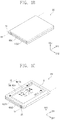
- FIGS. 1A, 1B, and 1C are perspective views of a display module according to some exemplary embodiments.
- FIG. 2 is a cross-sectional view of the display module of FIG. 1 according to some exemplary embodiments.
- FIG. 3 is a plan view of a display panel according to some exemplary embodiments.
- FIG. 4 is an equivalent circuit diagram of a pixel according to some exemplary embodiments.
- FIG. 5 is an enlarged cross-sectional view of the display panel of FIG. 1 according to some exemplary embodiments.
- FIG. 6A is a cross-sectional view of an input sensing unit according to some exemplary embodiments.
- FIG. 6B is a plan view of the input sensing unit of FIG. 6A according to some exemplary embodiments.
- FIG. 7A is a plan view of a first conductive layer of the input sensing unit of FIG. 6A according to some exemplary embodiments.
- FIG. 7B is a plan view of a second conductive layer of the input sensing unit of FIG. 6A according to some exemplary embodiments.
- FIG. 7C is a partial cross-sectional view of the input sensing unit of FIG. 6B taken along sectional line I-I′ according to some exemplary embodiments.
- FIG. 8A is a partial plan view of the input sensing unit of FIG. 6B according to some exemplary embodiments.
- FIG. 8B is an enlarged view of a portion AA of the input sensing unit of FIG. 8A according to some exemplary embodiments.
- FIG. 8C is an enlarged view of a portion BB of the input sensing unit of FIG. 8B according to some exemplary embodiments.
- FIG. 9A is a plan view of a portion of the input sensing unit of FIG. 6B according to some exemplary embodiments.
- FIG. 9B is a plan view representing outlined areas of first and second electrodes of the input sensing unit of FIG. 9A according to some exemplary embodiments.
- FIG. 9C is a plan view representing opening areas of the first and second electrodes of the input sensing unit of FIG. 9A according to some exemplary embodiments.
- FIG. 9D is a plan view representing effective areas of the first and second electrodes of the input sensing unit of FIG. 9A according to some exemplary embodiments.
- FIG. 9E is a plan view illustrating first and second sensing parts of the input sensing unit of FIG. 9A according to some exemplary embodiments.
- FIG. 10 is a plan view illustrating first and second sensing parts of an input sensing unit according to some exemplary embodiments.
- FIG. 11 is a plan view illustrating first and second sensing parts of an input sensing unit according to some exemplary embodiments.
- the illustrated exemplary embodiments are to be understood as providing exemplary features of varying detail of some exemplary embodiments. Therefore, unless otherwise specified, the features, components, modules, layers, films, panels, regions, aspects, etc. (hereinafter individually or collectively referred to as “elements”), of the various illustrations may be otherwise combined, separated, interchanged, and/or rearranged without departing from the spirit and the scope of the disclosure.
- the DR 1 -axis, the DR 2 -axis, and the DR 3 -axis are not limited to three axes of a rectangular coordinate system, and may be interpreted in a broader sense.
- the DR 1 -axis, the DR 2 -axis, and the DR 3 -axis may be perpendicular to one another, or may represent different directions that are not perpendicular to one another.
- “at least one of X, Y, and Z” and “at least one selected from the group consisting of X, Y, and Z” may be construed as X only, Y only, Z only, or any combination of two or more of X, Y, and Z, such as, for instance, XYZ, XYY, YZ, and ZZ.
- the term “and/or” includes any and all combinations of one or more of the associated listed items.
- Spatially relative terms such as “beneath,” “below,” “under,” “lower,” “above,” “upper,” “over,” and the like, may be used herein for descriptive purposes, and, thereby, to describe one element's relationship to another element(s) as illustrated in the drawings.
- Spatially relative terms are intended to encompass different orientations of an apparatus in use, operation, and/or manufacture in addition to the orientation depicted in the drawings. For example, if the apparatus in the drawings is turned over, elements described as “below” or “beneath” other elements or features would then be oriented “above” the other elements or features.
- the exemplary term “below” can encompass both an orientation of above and below.
- the apparatus may be otherwise oriented (e.g., rotated 90 degrees or at other orientations), and, as such, the spatially relative descriptors used herein interpreted accordingly.
- exemplary embodiments are described herein with reference to sectional and/or exploded illustrations that are schematic illustrations of idealized exemplary embodiments and/or intermediate structures. As such, variations from the shapes of the illustrations as a result, for example, of manufacturing techniques and/or tolerances, are to be expected. Thus, exemplary embodiments disclosed herein should not be construed as limited to the particular illustrated shapes of regions, but are to include deviations in shapes that result from, for instance, manufacturing. In this manner, regions illustrated in the drawings are schematic in nature and shapes of these regions may not illustrate the actual shapes of regions of a device, and, as such, are not intended to be limiting.
- FIGS. 1A, 1B, and 1C are perspective views of a display module according to some exemplary embodiments.
- a display surface IS on which an image IM is displayed is parallel to a surface defined by a first directional axis DR 1 and a second directional axis DR 2 .
- the normal direction of the display surface IS namely, the thickness direction of the display module DM, extends in a third directional axis DR 3 .
- a front surface (or top surface) and a rear surface (or bottom surface) of each member are distinguished by the third directional axis DR 3 .
- directions indicated by the first to third directional axes DR 1 , DR 2 , and DR 3 correspond to a relative concept and may be changed to other directions.
- the first to third directions are directions respectively indicated by the first to third directional axes DR 1 , DR 2 , and DR 3 , and refer to the same reference numerals.
- the display module DM may include a plurality of areas defined according to an operation type.
- the display module DM may include a bending area BA bended on the basis of a bending axis BX, a first non-bending area NBA 1 and a second non-bending area NBA 2 that are not bended.
- the display module DM may be inner-bended such that the display surface IS of the first non-bending area NBA 1 and the display surface IS of the second non-bending area NBA 2 face each other.
- the display module DM may be outer-bended such that the display surface IS is exposed externally.
- a display module DM in which the bending and unbending are repeated may be defined as a foldable display module DM.
- the display module DM in some exemplary embodiments may include a plurality of bending areas BA.
- the bending area BA may be defined to correspond to a type that enables a user to manipulate the display module DM.
- the bending area BA may be defined to be parallel to the second directional axis DR 2 or defined in a diagonal direction.
- the area of the bending area BA may not be fixed, but may be determined according to the radius of curvature.
- the display module DM in some exemplary embodiments may be configured such that only an operation mode illustrated in FIGS. 1A and 1B is repeated.
- the foldable display module DM is illustrated according to some exemplary embodiments, but exemplary embodiments are not limited thereto or thereby.
- the display module DM may include a three dimensional display surface (multilateral pillar type display surface) including a curved surface or a plurality of display areas indicating (or providing viewing surfaces in) different directions.
- the display module DM in some exemplary embodiments may be a flat rigid display module.
- the display module DM may be a bended type display module of which an edge area is bended.
- the display module DM is illustrated as being applied to a mobile phone, exemplary embodiments are not limited thereto or thereby.
- the display module DM in some exemplary embodiments, may be applied to a large electronic device, such as a television or a monitor, or a small and/or medium electronic device, such as a tablet, a vehicle navigation device, a game player, a smart watch, etc.
- the display surface IS includes a display area DM-DA on which an image IM is displayed and a non-display area DM-NDA adjacent to the display area DM-DA.
- the non-display area DM-NDA is an area on which the image is not displayed.
- icon images are illustrated in FIGS. 1A to 1C .
- the display area DM-DA may have a rectangular shape.
- the non-display area DM-NDA may surround the display area DM-DA.
- exemplary embodiments are not limited thereto or thereby, and the shapes of the display area DM-DA and the non-display area DM-NDA may be relatively designed.
- FIG. 2 is a cross-sectional view of the display module of FIG. 1 according to some exemplary embodiments. That is, FIG. 2 illustrates a cross-section of the display module DM defined by the second directional axis DR 2 and the third directional axis DR 3 .
- the display module DM includes a display panel DP and an input sensing unit TS (or touch sensing layer).
- the display panel DP generates an image and the input sensing unit TS acquires coordinate information about an external input (touch event).
- the display module DM may further include a protection member disposed on the bottom surface of the display panel DP and a reflection preventing member and/or a window member disposed on the top surface of the input sensing unit TS.
- the display panel DP may be a light emitting type display panel, however, exemplary embodiments are not limited thereto or thereby.
- the display panel DP may be an organic light emitting display panel or a quantum dot light emitting display panel.
- a light emitting layer of the organic light emitting display panel includes an organic light emitting material.
- a light emitting layer of the quantum dot light emitting display panel includes a quantum dot and a quantum rod.
- the display panel DP will be described as an organic light emitting display panel.
- the display panel DP includes a base layer SUB, a circuit element layer DP-CL disposed on the base layer SUB, a display element layer DP-OLED, and a thin film encapsulation layer TFE. Although not illustrated separately, the display panel DP may further include a functional layer, such as a reflection preventing layer or a refractive index adjusting layer.
- the base layer SUB may include a flexible film.
- the base layer SUB may include a plastic substrate, a glass substrate, a metal substrate, or an organic/inorganic compound material substrate, etc.
- the display area DM-DA and non-display area DM-NDA described in relation to FIGS. 1A to 1C may be identically defined on the base layer SUB.
- the circuit element layer DP-CL includes at least one intermediate insulation layer and a circuit element.
- the intermediate insulation layer includes at least one intermediate inorganic layer and at least one intermediate organic layer.
- the circuit element includes signal lines and a driving circuit of a pixel, etc.
- the circuit element layer DP-CL may be disposed through an insulation layer disposing process, such as coating or deposition process and a patterning process for a conductive layer and/or a semiconductor layer via a photolithography process.
- the display element layer DP-OLED may include an organic light emitting diode.
- the display element layer DP-OLED may further include an organic layer, such as a pixel definition layer.
- the thin film encapsulation layer TFE encapsulates the display element layer DP-OLED.
- the thin film encapsulation layer TFE includes at least one inorganic layer (hereinafter, an encapsulation inorganic layer).
- the thin film encapsulation layer TFE may further include at least one organic layer (hereinafter, an encapsulation organic layer).
- the encapsulation inorganic layer protects the display element layer DP-OLED from moisture, oxygen, etc., and protects the display element layer DP-OLED from a foreign material, such as a dust particle or other debris.
- the encapsulation inorganic layer may include a silicon nitride layer, a silicon oxy-nitride layer and a silicon oxide layer, a titanium oxide layer, or an aluminum oxide layer, etc.
- the encapsulation inorganic layer may include an acrylic-based inorganic layer, but exemplary embodiments are not limited thereto or thereby.
- the input sensing unit TS may be directly disposed on a base surface provided by the display panel DP.
- being “directly disposed” means exclusion of being attached using a separate adhesive layer, and means being disposed by a continuous process.
- the base surface may be the top surface of the thin film encapsulation layer TFE or of another function layer disposed on the thin film encapsulation layer TFE.
- the base surface is not limited thereto or thereby, and the uppermost surface of the display panel DP provided by the continuous process is sufficient therefor.
- the input sensing unit TS being directly disposed on the base surface provided via the display panel DP results in the omission of a separate base substrate of the input sensing unit TS, and thus, the thickness of the display module DM is decreased.
- the input sensing unit TS may have a multi-layer structure.
- the input sensing unit TS may include a conductive layer of a single layer or multiple layers.
- the input sensing unit TS may include at least one insulation layer.
- the input sensing unit TS may sense an external input, for example, in a capacitive manner.
- An operation manner of the input sensing unit TS is not limited thereto or thereby, and the input sensing unit TS in some exemplary embodiments may sense an external input in a electromagnetic inductive manner, a pressure sensing manner, etc.
- FIG. 3 is a plan view of a display panel according to some exemplary embodiments.
- FIG. 4 is an equivalent circuit diagram of a pixel according to some exemplary embodiments.
- FIG. 5 is an enlarged cross-sectional view of the display panel of FIG. 1 according to some exemplary embodiments.
- the display panel DP includes the display area DA and the non-display area NDA on a plane.
- the non-display area NDA in some exemplary embodiments may be defined according to an edge of the display area DA.
- the display area DA and the non-display area NDA of the display panel DP may respectively correspond to the display area DM-DA and the non-display area DM-NDA of the display module DM illustrated in FIGS. 1A to 1C .
- the display area DA and the non-display area NDA of the display panel DP may not be necessarily identical to the display area DM-DA and the non-display area DM-NDA of the display module DM, and may be changed according to the structure and/or design of the display panel DP.
- the display panel DP may include a driving circuit GDC, a plurality of signal lines SGL, and a plurality of pixels PX.
- the plurality of pixels PX are disposed in the display area DA.
- Each of the pixels PX includes an inorganic light emitting diode and a pixel driving circuit connected thereto.
- the driving circuit GDC, the plurality of signal lines SGL, and the pixel driving circuit may be included in the circuit element layer DP-CL illustrated in FIG. 2 .
- the driving circuit GDC may include a gate driving circuit, and, as such, these terms may be interchangeably utilized herein.
- the gate driving circuit GDC generates a plurality of gate signals and sequentially outputs the plurality of gate signals to the plurality of gate lines GL to be described later.
- the gate driving circuit GDC may further output another control signal to the driving circuit of the pixels PX.
- the gate driving circuit GDC may include a plurality of thin-film transistors provided through the same process as that of the driving circuit of the pixels PX, for example, a low temperature polycrystalline silicon (LTPS) process or a low temperature polycrystalline oxide (LTPO) process.
- LTPS low temperature polycrystalline silicon
- LTPO low temperature polycrystalline oxide
- the plurality of signal lines SGL may include the gate lines GL, data lines DL, a power supply line PL, and a control signal line CSL.
- the gate lines GL are respectively connected to corresponding pixels PX from among the plurality of pixels PX and the data lines DL may be respectively connected to corresponding pixels PX from among the plurality of pixels PX.
- the power supply line PL is connected to the plurality of pixels PX.
- the control signal line CSL may provide control signals to the gate driving circuit GDC.
- the display panel DP includes signal pads DP-PD connected to terminals of the signal lines SGL.
- the signal pads DP-PD may be a kind of circuit elements.
- An area in which the signal pads DP-PD are disposed in the non-display area NDA is defined as a pad area NDA-PD.
- dummy pads TS-DPD to be connected to signal lines SL 1 - 1 to SL 1 - 5 and SL 2 - 1 to SL 2 - 4 to be described later may be further disposed.
- the signal pads DP-PD and the dummy pads TS-DPD may be disposed on an identical layer through the same process as that of the gate lines GL (see FIG. 5 ) or data lines DL (see FIG. 5 ) to be described later.
- the pixel PX connected to any one gate line GL, any one data line DL, and the power supply line PL are exemplarily illustrated.
- the configuration of the pixel PX is not limited thereto ore thereby, but may be modified in any suitable manner.
- the organic light emitting diode OLED may be a front surface type light emitting diode (LED) or a rear surface type LED.
- the pixel PX includes a first transistor T 1 (or a switching transistor), a second transistor T 2 (or a driving transistor), and a capacitor Cst, as a pixel driving circuit for driving the organic light emitting diode OLED.
- a first power supply voltage ELVDD is provided to the second transistor T 2
- a second power supply voltage ELVSS is provided to the organic light emitting diode OLED.
- the second power supply voltage ELVSS may be lower than the first power supply voltage ELVDD.
- the first transistor T 1 outputs a data signal applied to the data line DL in response to the gate signal applied to the gate line GL.
- the capacitor Cst charges a voltage corresponding to the data signal received from the first transistor T 1 .
- the second transistor T 2 is connected to the organic light emitting diode OLED.
- the second transistor T 2 controls a driving current flowing through the organic light emitting diode OLED in response to a charge amount stored in the capacitor Cst.
- FIG. 5 illustrates a partial cross-section of the display panel DP corresponding to the equivalent circuit illustrated in FIG. 4 .
- the circuit element layer DP-CL, the display element layer DP-OLED, and the thin film encapsulation layer TFE are sequentially disposed on the base layer SUB.
- the circuit element layer DP-CL includes at least one inorganic layer, at least one organic layer, and a circuit element.
- the circuit element layer DP-CL includes a buffer layer BFL that is an inorganic layer, a first intermediate inorganic layer 10 , and a second intermediate inorganic layer 20 , and may further include an intermediate organic layer 30 that is an organic layer.
- the inorganic layers may include silicon nitride, silicon oxy-nitride and silicon oxide, etc.
- the organic layer may include at least one of an acrylic based resin, a meta-acrylic based resin, polyisoprene, a vinyl based resin, an epoxy based resin, an urethane based resin, a cellulose based resin, a siloxane based resin, a polyimide based resin, a polyamide resin, or a parylene based resin.
- the circuit element includes conduction patterns and/or semiconductor patterns.
- the buffer layer BFL enhances a binding force between the base layer SUB and the conductive patterns or the semiconductor patterns.
- a barrier layer preventing a foreign material from flowing in may be further disposed on the top surface of the base layer SUB.
- the buffer layer BFL and the barrier layer may be selectively disposed or omitted.
- a semiconductor pattern OSP 1 (hereinafter, a first semiconductor pattern) of the first transistor T 1 and a semiconductor pattern T 2 OSP 2 (hereinafter, a second semiconductor pattern) of the second transistor T 2 are disposed on the buffer layer BFL.
- the first semiconductor pattern OSP 1 and the second semiconductor pattern OSP 2 may be selected from among amorphous silicon, polycrystalline silicon, and metal oxide semiconductor.
- the first intermediate inorganic layer 10 is disposed on the first semiconductor pattern OSP 1 and the second semiconductor inorganic layer OSP 2 .
- a control electrode GE 1 (hereinafter, a first control electrode) of the first transistor T 1 and a control electrode GE 2 (hereinafter, a second control electrode) of the second transistor T 2 are disposed on the first intermediate inorganic layer 10 .
- the first control electrode GE 1 and the second control electrode GE 2 may be manufactured according to the same photolithography process as that of the gate lines GL (see FIG. 5A ).
- the second intermediate inorganic layer 20 covering the first control electrode GE 1 and the second control electrode GE 2 is disposed on the first intermediate inorganic layer 10 .
- An input electrode DE 1 (hereinafter, a first input electrode) of the first transistor T 1 and an input electrode DE 2 (hereinafter, a second input electrode) of the second transistor T 2 are disposed on the second intermediate inorganic layer 20 .
- the first input electrode DE 1 and a first output electrode SE 1 are connected to the first semiconductor pattern OSP 1 respectively through a first through hole CH 1 and a second through hole CH 2 respectively penetrating through the first intermediate inorganic layer 10 and the second intermediate inorganic layer 20 .
- the second input electrode DE 2 and a second output electrode SE 2 are connected to the second semiconductor pattern OSP 2 respectively through a third through hole CH 3 and a fourth through hole CH 4 respectively penetrating through the first intermediate inorganic layer 10 and the second intermediate inorganic layer 20 .
- a part of the first transistor T 1 and the second transistor T 2 may be modified as a bottom-gate structure, a dual-gate structure, etc.
- the intermediate organic layer 30 covering the first input electrode DE 1 , the second input electrode DE 2 , the first output electrode SE 1 , and the second output electrode SE 2 is disposed on the second intermediate inorganic layer 20 .
- the intermediate organic layer 30 may provide a flat plane.
- the display element layer DP-OLED is disposed on the intermediate organic layer 30 .
- the display element layer DP-OLED may include the pixel definition layer PDL and the organic light emitting diode OLED.
- the pixel definition layer PDL may include an organic material, like the intermediate organic layer 30 .
- a first electrode AE is disposed on the intermediate organic layer 30 .
- the first electrode AE is connected to the second output electrode SE 2 through a fifth through hole CH 5 penetrating through the intermediate organic layer 30 .
- An opening OP is defined in the pixel definition layer PDL.
- the opening OP of the pixel definition layer PDL exposes at least a part of the first electrode AE.
- the pixel PX may be disposed on a pixel area on the plane.
- the pixel area may include the light emitting area PXA and a non-light emitting area NPXA adjacent to the light emitting area PXA.
- the non-light emitting area NPXA may surround the light emitting area PXA.
- the light emitting area PXA is defined to correspond to a partial area of the first electrode AE exposed by the opening OP.
- a hole control layer HCL may be commonly disposed on the light emitting area PXA and the non-light emitting area NPXA. Although not illustrated separately, a common layer, such as the hole control layer HCL, may be commonly disposed on the plurality of pixels PX (see FIG. 3 ).
- An emission material layer EML is disposed on the hole control layer HCL.
- the emission material layer EML may be disposed on an area corresponding to the opening OP. In other words, the emission material layer EML may be separately disposed on each of the plurality of pixels PX.
- the emission material layer EML may include an organic material and/or an inorganic material. In some exemplary embodiments, a patterned emission material layer EML is exemplarily illustrated, but the emission material layer EML may be commonly disposed on the plurality of pixels PX.
- the emission material layer EML may generate white light, however, exemplary embodiments are not limited thereto or thereby.
- the emission material layer EML may have a multilayer structure.
- An electron control layer ECL is disposed on the emission material layer EML. Although not illustrated separately, the electron control layer ECL may be commonly disposed on the plurality of pixels PX (see FIG. 3 ).
- a second electrode CE is disposed on the electron control layer ECL.
- the second electrode CE is commonly disposed on the plurality of pixels PX.
- the thin film encapsulation layer TFE is disposed on the second electrode CE.
- the thin film encapsulation layer TFE is commonly disposed on the plurality of pixels PX.
- the thin film encapsulation layer TFE directly covers the second electrode CE.
- a capping layer covering the second electrode CE may be further disposed between the thin film encapsulation layer TFE and the second electrode CE.
- the thin film encapsulation layer TFE may directly cover the capping layer.
- FIG. 6A is a cross-sectional view of an input sensing unit according to some exemplary embodiments.
- FIG. 6B is a plan view of the input sensing unit of FIG. 6A according to some exemplary embodiments.
- FIG. 7A is a plan view of a first conductive layer of the input sensing unit of FIG. 6A according to some exemplary embodiments.
- FIG. 7B is a plan view of a second conductive layer of the input sensing unit of FIG. 6A according to some exemplary embodiments.
- FIG. 7C is a partial cross-sectional view of the input sensing unit of FIG. 6B taken along sectional line I-I′ according to some exemplary embodiments.
- FIG. 6A as a configuration of the display panel DP (see FIG. 5 ), the second electrode CE and the thin film encapsulation layer TFE are illustrated.
- the input sensing unit TS includes a first conductive layer TS-CL 1 , a first insulation layer TS-IL 1 , a second conductive layer TS-CL 2 , and a second insulation layer TS-IL 2 .
- the first conductive layer TS-CL 1 is directly disposed on the thin film encapsulation layer TFE, but exemplary embodiments are not limited thereto or thereby.
- another inorganic layer or organic layer may be further disposed between the first conductive layer TS-CL 1 and the thin film encapsulation layer TFE.
- the second insulation layer TS-IL 2 may be omitted, and an optical member or an adhesive layer, etc., may replace a protection function of the second insulation layer TS-IL 2 .
- Each of the first conductive layer TS-CL 1 and the second conductive layer TS-CL 2 may have a single layer structure or a multilayer structure along the third directional axis DR 3 .
- a conductive layer of a single layer structure may include a metal layer or a transparent conductive layer.
- the metal layer may include, for instance, at least one of molybdenum, silver, titanium, copper, aluminum, and an alloy thereof.
- the transparent conductive layer may include, for example, at least one of a transparent conductive oxide, such as indium tin oxide (ITO), indium zinc oxide (IZO), zinc oxide (ZnO), or indium tin zinc oxide (ITZO).
- the transparent conductive layer may include at least one of a conductive polymer, e.g., poly(3,4-ethylenedioxythiophene) (PEDOT), etc., a metal nano-wire, and graphene.
- a conductive layer of a multilayer structure may include a multi-layered metal layer.
- the multi-layered metal layer may have a three-layered structure of titanium/aluminum/titanium.
- a conductive layer of a multilayer structure may include a single metal layer and a transparent conductive layer.
- a conductive layer of a multilayer structure may include a multi-layered metal layer and a transparent conductive layer.
- each of the first conductive layer TS-CL 1 and the second conductive layer TS-CP 2 includes a plurality of conductive patterns.
- the conductive patterns may include electrodes and signal lines.
- Each of the first insulation layer TS-IL 1 and the second insulation layer TS-IL 2 may include an inorganic material or an organic material. At least one of the first insulation layer TS-IL 1 and the second insulation layer TS-IL 2 may include an inorganic layer.
- the inorganic layer may include at least one of aluminum oxide, titanium oxide, silicon oxide, silicon oxynitride, zirconium oxide, and hafnium oxide. At least one of the first insulation layer TS-IL 1 and the second insulation layer TS-IL 2 may include an organic layer.
- the organic layer may include at least one of an acrylic based resin, a meta-acrylic based resin, polyisoprene, a vinyl based resin, an epoxy based resin, an urethane based resin, a cellulose based resin, a siloxane based resin, a polyimide based resin, a polyamide resin, and a parylene based resin.
- the input sensing unit TS may include first electrodes TE 1 - 1 to TE 1 - 5 , first signal lines SL 1 - 1 to SL 1 - 5 connected to the first electrodes TE 1 - 1 to TE 1 - 5 , second electrodes TE 2 - 1 to TE 2 - 4 , second signal lines SL 2 - 1 to SL 2 - 4 connected to the second electrodes TE 2 - 1 to TE 2 - 5 , and touch pads TS-PD connected to the first signal lines SL 1 - 1 to SL 1 - 5 and the second signal lines SL 2 - 1 to SL 2 - 4 .
- first electrodes TE 1 - 1 to TE 1 - 5 and the second electrodes TE 2 - 1 to TE 2 - 4 intersect with each other, but the first electrodes TE 1 - 1 to TE 1 - 5 and the second electrodes TE 2 - 1 to TE 2 - 4 are insulated from one another.
- the first electrodes TE 1 - 1 to TE 1 - 5 are arrayed in the second direction DE 2 , each of which has a shape extending toward the first direction DR 1 .
- the second electrodes TE 2 - 1 to TE 2 - 5 are arrayed in the first direction DR 1 , each of which has a shape extending toward the second direction DR 2 .
- first electrodes TE 1 - 1 to TE 1 - 5 Although particular numbers of the first electrodes TE 1 - 1 to TE 1 - 5 , the first signal lines SL 1 - 1 to SL 1 - 5 , the second electrodes TE 2 - 1 to TE 2 - 4 , the second signal lines SL 2 - 1 to SL 2 - 4 , and the touch pads TS-PD are shown, exemplary embodiments are not limited thereto or thereby.
- any suitable number of the first electrodes TE 1 - 1 to TE 1 - 5 , the first signal lines SL 1 - 1 to SL 1 - 5 , the second electrodes TE 2 - 1 to TE 2 - 4 , the second signal lines SL 2 - 1 to SL 2 - 4 , and the touch pads TS-PD may be utilized.
- Each of the first electrodes TE 1 - 1 to TE 1 - 5 has a first length and each of the second electrodes TE 2 - 1 to TE 2 - 4 has a second length.
- the first length extends toward the first direction DR 1
- the second length extends toward the second direction DR 2 .
- the second length is longer than the first length.
- the second electrodes TE 2 - 1 to TE 2 - 4 since the second electrodes TE 2 - 1 to TE 2 - 4 have more sensors than the first electrodes TE 1 - 1 to TE 1 - 5 , the second electrodes TE 2 - 1 to TE 2 - 4 have a longer length than the first electrodes TE 1 - 1 to TE 1 - 5 .
- the first signal lines SL 1 - 1 to SL 1 - 5 are respectively connected to one (e.g., first) ends of the first electrodes TE 1 - 1 to TE 1 - 5 .
- the second signal lines SL 2 - 1 to SL 2 - 4 are respectively connected to both (e.g., first and second) ends of the second electrodes TE 2 - 1 to TE 2 - 4 .
- the first signal lines SL 1 - 1 to SL 1 - 5 may also be respectively connected to both ends of the first electrodes TE 1 - 1 to TE 1 - 5 .
- the second signal lines SL 2 - 1 to SL 2 - 4 may be respectively connected to only one ends of the second electrodes TE 2 - 1 to TE 2 - 4 .
- the first signal lines SL 1 - 1 to SL 1 - 5 , the second signal lines SL 2 - 1 to SL 2 - 4 , and the touch pads TS-PD may be replaced by a circuit board, etc., that is separately manufactured and coupled as part of the display module DM.
- the touch pads TS-PD may be omitted, and the first signal lines SL 1 - 1 to SL 1 - 5 and the second signal lines SL 2 - 1 to SL 2 - 4 may be connected to the dummy pads TS-DPD illustrated in FIG. 3 .
- the input sensing unit TS may sense an external input in a mutual capacitive-type or a self-capacitive type.
- the input sensing unit TS includes at least one insulation layer.
- each of the first electrodes TE 1 - 1 to TE 1 - 5 includes first sensing parts SP 1 and first connecting parts CP 1 .
- Each of the second electrodes TE 2 - 1 to TE 2 - 4 includes second sensing parts SP 2 and second connecting parts CP 2 .
- the first sensing parts SP 1 are arrayed along the first direction DR 1 and the second sensing parts SP 2 are arrayed along the second direction DR 2 .
- Each of the first connecting parts CP 1 connects adjacent sensing parts SP 1 and each of the second connecting parts CP 2 connects adjacent second sensing parts SP 2 .
- the second electrodes TE 2 - 1 to TE 2 - 4 which are longer than the first electrodes TE 1 - 1 to TE 1 - 5 , include a larger number of sensing parts and connecting parts. Accordingly, the second electrodes TE 2 - 1 to TE 2 - 4 may have larger outlined areas than the first electrodes TE 1 - 1 to TE 1 - 5 .
- the “outlined area” is an area defined by an outline of an associated electrode, as will become more apparent below.
- the outlined areas of the first sensing part SP 1 and the second sensing part SP 2 may be identical. Accordingly, the outlined areas of the first electrodes TE 1 - 1 to TE 1 - 5 and the second electrodes TE 2 - 1 to TE 2 - 4 may be respectively proportional to the respective numbers of included sensing parts.
- FIG. 6B exemplarily illustrates the first electrodes TE 1 - 1 to TE 1 - 5 including five first sensing parts SP 1 and the second electrodes TE 2 - 1 to TE 2 - 4 including six second sensing parts SP 2 .
- Two first sensing parts SP 1 (hereinafter, first half sensing parts) disposed on both ends of the five first sensing parts SP 1 may have a size of half the first sensing parts disposed in the central region.
- Two second sensing part SP 2 (hereinafter, second half sensing parts) disposed on both ends of the six second sensing part SP 2 may have a size of half the second sensing parts disposed in the central region.
- the two first half sensing parts and the two second half sensing parts are treated as one sensing part in calculating (or otherwise determining) outlined areas, opening areas, and effective areas that will be described later in more detail.
- the first connecting parts CP 1 are disposed on the thin film encapsulation layer TFE, e.g., between the first insulation layer TS-IL 1 and the thin film encapsulation layer TFE.
- the first connecting parts CP 1 may include a transparent conductive oxide and/or a metal.
- the first connecting parts CP 1 may include a multi-layered metal layer.
- the second connecting parts CP 2 may be disposed on the thin film encapsulation layer TFE, e.g., between the first insulation layer TS-IL 1 and the thin film encapsulation layer TFE.
- the first insulation layer TS-IL 1 covering the first connecting parts CP 1 is disposed on the thin film encapsulation layer TFE.
- Contact holes CH 10 exposing portions of the first connecting parts CP 1 are defined in the first insulation layer TS-IL 1 .
- the first sensing parts SP 1 and the second sensing parts SP 2 are disposed on the first insulation layer TS-IL 1 .
- the second connecting parts CP 2 are disposed on the first insulation layer TS-IL 1 .
- the second sensing parts SP 2 and the second connecting parts CP 2 may be provided through an identical photolithography process, and, thereby, may have an integrated shape.
- the second connecting parts CP 2 may extend from the second sensing parts SP 2 .
- the first sensing parts SP 1 , the second sensing parts SP 2 , and the second connecting parts CP 2 may include a transparent conductive oxide and/or a metal.
- the first sensing parts SP 1 , the second sensing parts SP 2 , and the second connecting parts CP 2 may include a multi-layered metal layer, for example, a titanium/aluminum/titanium metal layer.
- the first signal lines SL 1 - 1 to SL 1 - 5 and the second signal lines SL 2 - 1 to SL 2 - 4 are disposed on the first insulation layer TS-IL 1 .
- the first signal lines SL 1 - 1 to SL 1 - 5 and the second signal lines SL 2 - 1 to SL 2 - 4 may be provided through the same process as that of the first sensing parts SP 1 , and, thereby, may have an identical laminated structure.
- the second conductive layer TS-CL 2 includes the first sensing parts SP 1 and the second sensing parts SP 2 to maintain a greater distance (e.g., spacing in the third directional axis DR 3 ) from the second electrode CE of the display panel DP.
- the input sensing unit TS may reduce parasitic capacitance Cbc between the second electrode CE and the first sensing parts SP 1 and the second sensing parts SP 2 .
- the distance between the second electrode CE and the first sensing parts SP 1 and the second sensing parts SP 2 may be about 0.5 ⁇ m to about 5 ⁇ m.
- the sum of the thicknesses of insulation layers disposed between the second electrode CE and the first sensing parts SP 1 and the second sensing parts SP 2 for example, the thin film encapsulation layer TFE and the first insulation layer TS-IL 1 , may be about 0.5 ⁇ m to about 30 ⁇ m.
- the thickness of an insulation layer disposed between the second electrode CE and the first sensing parts SP 1 and the second sensing parts SP 2 may be about 0.5 ⁇ m to about 10 ⁇ m, e.g., about 0.5 ⁇ m to about 5 ⁇ m.
- the second conductive layer TS-CL 2 may reduce parasitic capacitance by including the first sensing parts SP 1 and the second sensing parts SP 2 .
- Exemplary embodiments are not limited to or by the above-noted structure of the input sensing unit TS.
- components of the first conductive layer TS-CL 1 and the second conductive layer TS-CL 2 may be changed with respect to each other.
- the second connecting parts CP 2 may be disposed on an upper surface of the first insulation layer TS-IL 1
- the first sensing parts SP 1 , the second sensing parts SP 2 , and the first connecting parts CP 1 may be disposed on a lower surface of the first insulation layer TS-IL 1 .
- FIG. 8A is a partial plan view of the input sensing unit of FIG. 6B according to some exemplary embodiments.
- FIG. 8B is an enlarged view of a portion AA of the input sensing unit of FIG. 8A according to some exemplary embodiments.
- FIG. 8C is an enlarged view of a portion BB of the input sensing unit of FIG. 8B according to some exemplary embodiments.
- FIG. 8A illustrates an enlarged area corresponding to two first sensing parts SP 1 and two second sensing parts SP 2 .
- the first sensing parts SP 1 include a first center part CTP 1 and a first edge part EP 1
- the second senor units SP 2 include a second center part CTP 2 and the second edge part EP 2
- At least one first opening SP-OP 1 is defined in the first center part CTP 1
- at least one opening SP-OP 2 is defined in the second center part CTP 2
- FIG. 8A exemplarily illustrates sixteen (16) first openings SP-OP 1 disposed in a matrix type and thirty six (36) second openings SP-OP 2 disposed in a matrix type; however, exemplary embodiments are not limited thereto or thereby.
- the first openings SP-OP 1 and the second openings SP-OP 2 may be provided in an identical number. As shown, however, the first openings SP-OP 1 occupy a smaller area than the second openings SP-OP 2 .
- the definition of the openings in each of the first sensing parts SP 1 and the second sensing parts SP 2 may cause reduction in the parasitic capacitance Cbc between the second electrode CE and the first sensing parts SP 1 and the second sensing parts SP 2 described in relation to FIG. 7C , e.g., the parasitic capacitance between the second electrode CE and the first electrodes TE 1 - 1 to TE 1 - 5 and the second electrodes TE 2 - 1 to TE 2 - 4 (see FIG. 6B ).
- a capacitance change amount value between the first sensing part SP 1 and the second sensing part SP 2 may be maintained equal to or greater than a reference value at least because facing areas between the first sensing parts SP 1 and the second sensing parts SP 2 may exert a greater influence on capacitance.
- the capacitance change amount is a difference value between capacitances before and after a touch event occurs.
- the first electrodes TE 1 - 1 to TE 1 - 5 have a first opening area due to the first openings SP-OP 1 and the second electrodes TE 2 - 1 to TE 2 - 4 have a second opening area due to the second openings SP-OP 2 .
- the first opening area is defined as a sum of total areas of the first openings SP-OP 1 and the second opening area is defined as a sum of total areas of the second openings SP-OP 2 .
- the second opening area is greater than the first opening area.
- Deviations in parasitic capacitance, which are generated in the first electrodes TE 1 - 1 to TE 1 - 5 and the second electrodes TE 2 - 1 to TE 2 - 4 may be reduced by providing a greater opening area to the second electrodes TE 2 - 1 to TE 2 - 4 of which the outlined area is greater than that the outline area of the first electrodes TE 1 - 1 to TE 1 - 5 .
- the first electrodes TE 1 - 1 to TE 1 - 5 and the second electrodes TE 2 - 1 to TE 2 - 4 may have a mesh shape to reduce the parasitic capacitance Cbc.
- first electrodes TE 1 - 1 to TE 1 - 5 and the second electrodes TE 2 - 1 to TE 2 - 4 will be provided.
- the first sensing part SP 1 and the second sensing part SP 2 may include mesh lines.
- the first connecting part CP 1 and the second connecting part CP 2 also may have mesh lines.
- the second sensing part SP 2 does not overlap the light emitting areas PXA-R, PXA-G, and PXA-B, but overlaps the non-light emitting areas NPXA (see FIG. 5 ).
- the light emitting areas PXA-R, PXA-G, and PXA-B may be defined as the light emitting area PXA of FIG. 5 .
- the mesh lines of the second sensing part SP 2 define a plurality of mesh holes TS-OPR, TS-OPG, and TS-OPB.
- the line width of the mesh lines may be several ⁇ m to several nm.
- the plurality of mesh holes TS-OPR, TS-OPG, and TS-OPB are defined in the second sensing part SP 2 .
- the plurality of mesh holes TS-OPR, TS-OPG, and TS-OPB may be in one-to-one correspondence with the light emitting areas PXA-R, PXA-G, and PXA-B.
- the light emitting areas PXA-R, PXA-G, and PXA-B are disposed separately from each other and the non-light emitting areas NPXA are disposed therebetween.
- a corresponding organic light emitting diode OLED is disposed for each of the light emitting areas PXA-R, PXA-G, and PXA-B.
- the light emitting areas PXA-R, PXA-G, and PXA-B may be divided into several groups according to colors of light generated by the corresponding organic light emitting diodes OLEDs.
- FIG. 8C illustrates the light emitting areas PXA-R, PXA-G, and PXA-B divided into three groups according to the emitted light colors of corresponding organic light emitting diodes OLEDs.
- the light emitting areas PXA-R, PXA-G, and PXA-B may have different areas according to light colors emitted by the emission material layer EML (see FIG. 6C ) of the organic light emitting diodes OLEDs (see FIG. 5 ).
- the areas of the light emitting areas PXA-R, PXA-G, and PXA-B may be determined. For instance, the light emitting area PXA-B may be the largest, the light emitting area PXA-G may be the smallest, and the light emitting area PXA-R may be sized between the light emitting areas PXA-B and PXA-G. Exemplary embodiments, however, are not limited thereto or thereby.
- the plurality of mesh holes TS-OPR, TS-OPG, and TS-OPB may be divided into several groups having different areas.
- the plurality of mesh holes TS-OPR, TS-OPG, and TS-OPB may be divided into three groups according to the corresponding light emitting areas PXA-R, PXA-G, and PXA-B.
- the plurality of mesh holes TS-OPR, TS-OPG, and TS-OPB have been described to be in one-to-one correspondence with the light emitting areas PXA-R, PXA-G, and PXA-B, but exemplary embodiments are not limited thereto or thereby.
- one mesh hole TS-OPR, TS-OPG, or TS-OPB may be in one-to-one correspondence with two or more light emitting areas PXA-R, PXA-G, and PXA-B.
- the various areas of the light emitting areas PXA-R, PXA-G, and PXA-B are exemplarily illustrated, but exemplary embodiments are not limited thereto or thereby.
- the sizes of the light emitting areas PXA-R, PXA-G, and PXA-B may be identical and the sizes of the mesh holes TS-OPR, TS-OPG, and TS-OPB may also be identical.
- first dummy electrodes DM 1 may be disposed the inner side of the first openings SP-OP 1 and second dummy electrodes DM 2 may be disposed the inner side of the second openings SP-OP 2 .
- the first dummy electrodes DM 1 may be respectively disposed on (or in) the first openings SP-OP 1 and the second dummy electrodes DM 2 may be respectively disposed on (or in) the second openings SP-OP 2 .
- the first dummy electrodes DM 1 and the second dummy electrodes DM 2 may be floating electrodes. Accordingly, the first dummy electrodes DM 1 and the second dummy electrodes DM 2 do not influence the parasitic capacitance Cbc of the first electrodes TE 1 - 1 to TE 1 - 5 and the second electrodes TE 2 - 1 to TE 2 - 5 .
- the first dummy electrodes DM 1 and the second dummy electrodes DM 2 are disposed on (or in) the first openings SP-OP 1 and the second openings SP-OP 2 to increase an external light reflectivity of the first openings SP-OP 1 and the second openings SP-OP 2 to a level similar to a reflectivity of another area of a corresponding one of the first electrodes TE 1 - 1 to TE 1 - 5 or a corresponding one of the second electrodes TE 2 - 1 to TE 2 - 5 .
- the first dummy electrodes DM 1 and the second dummy electrodes DM 2 may include mesh lines.
- the first dummy electrodes DM 1 and the second dummy electrodes DM 2 may have the same characteristics (e.g., configuration) as the mesh lines of the second sensing part SP 2 illustrated in FIG. 8C .
- FIG. 9A is a plan view of a portion of the input sensing unit of FIG. 6B according to some exemplary embodiments.
- FIG. 9B is a plan view representing outlined areas of first and second electrodes of the input sensing unit of FIG. 9A according to some exemplary embodiments.
- FIG. 9C is a plan view representing opening areas of the first and second electrodes of the input sensing unit of FIG. 9A according to some exemplary embodiments.
- FIG. 9D is a plan view representing effective areas of the first and second electrodes of the input sensing unit of FIG. 9A according to some exemplary embodiments.
- FIG. 9E is a plan view illustrating first and second sensing parts of the input sensing unit of FIG. 9A according to some exemplary embodiments. For instance, FIG.
- FIG. 9B provides a plan view representing outlined areas of the first electrode TE 1 - 4 and the second electrode TE 2 - 2
- FIG. 9C provides a plan view representing the opening areas of the first electrode TE 1 - 4 and the second electrode TE 2 - 2
- FIG. 9D provides a plan view representing the effective areas of the first electrode TE 1 - 4 and the second electrode TE 2 - 2
- FIG. 9E provides a plan view illustrating the first sensing part SP 1 and the second sensing part SP 2 . In this manner, FIGS.
- 9A to 9E exemplarily illustrate the fourth, first electrode TE 1 - 4 as a representative first electrode among the first electrodes TE 1 - 1 to TE 1 - 5 and the second, second electrode TE 2 - 2 as a representative electrode among the second electrodes TE 2 - 1 to TE 2 - 4 illustrated in FIG. 6B .
- the second, second electrode TE 2 - 2 has a larger outlined area (the area indicated by hatching in FIG. 9B ) than the first, fourth electrode TE 1 - 4 .
- the areas of the second, second electrode TE 2 - 2 and the first, fourth electrode TE 1 - 4 may be determined according to the number of sensing parts respectively provided therein.
- the second, second electrode TE 2 - 2 has the outlined area corresponding to five second sensing parts SP 2
- the first, fourth electrode TE 1 - 4 has the outlined area corresponding to four second sensing parts SP 2 .
- the second sensing part SP 2 and the first sensing part SP 1 may have the same outlined area and shape.
- an opening area (an area indicated by hatching in FIG. 9C , hereinafter, a second opening area SP-OP 2 ) of the second, second electrode TE 2 - 2 is greater than an opening area (an area indicated by hatching in FIG. 9C , hereinafter, a first opening area SP-OP 1 ) of the first, fourth electrode TE 1 - 4 .
- the first opening area SP-OP 1 and the second opening area SP-OP 2 may be defined such that the first and second effective areas to be described in relation to FIG. 9D are substantially identical.
- the effective area (an area indicated by hatching in FIG. 9D , hereinafter the second effective area) of the second, second electrode TE 2 - 2 illustrated in FIG. 9D may be substantially identical to the effective area (an area indicated by hatching in FIG. 9D , hereinafter the first effective area) of the first electrode TE 1 - 4 .
- the first and second effective areas may be respectively obtained by subtracting the first opening areas SP-OP 1 and the second opening areas SP-OP 2 shown in FIG. 9C from the first outlined area and the second outlined area shown in FIG. 9B .
- the effective area may be an area in which the mesh lines described in relation to FIGS. 8A to 8C are disposed.
- the phrase “the effective areas are substantially identical” means that the effective areas are identical when they include the areas of the first connecting parts CP 1 and the second connecting parts CP 2 , which are relatively smaller than those of the first sensing parts SP 1 and the second sensing parts SP 2 .
- the effective areas of the first, fourth electrode TE 1 - 4 and the second, second electrode TE 2 - 2 are identical, a deviation in parasitic capacitance Cbc generated in the first, fourth electrode TE 1 - 4 and the second, second electrode TE 2 - 2 (see FIG. 7C ), which has been described in relation to FIG. 7C , may be reduced. Even if the first and second effective areas are not substantially identical, in order to reduce the deviation in the parasitic capacitance Cbc, the first effective area may be 95% to 105% of the second effective area.
- the outlined areas and shapes of the first sensing part SP 1 and the second sensing part SP 2 may be identical.
- the second, second electrode TE 2 - 2 may have the outlined area of about X/Y ⁇ 100% in comparison to the first, fourth electrode TE 1 - 4 .
- the second, second electrode TE 2 - 2 illustrated in FIG. 9B may have the outlined area of about 125% in comparison to the first, fourth electrode TE 1 - 4 .
- the second sensing parts SP 2 may have the effective area of about Y/X ⁇ 100% in comparison to the first sensing parts SP 1 .
- the second sensing parts SP 2 illustrated in FIG. 9B may have the effective area of about 80% in comparison to the first sensing parts SP 1 .
- the first effective area is about 10% to about 70% in comparison to the first outlined area, and the second effective area is about 30% to 90% in comparison to the second outlined area.
- the first openings SP-OP 1 and the second openings SP-OP 2 illustrated in FIG. 9E have identical shapes, but exemplary embodiments are not limited thereto or thereby.
- a determination factor of the outlined area of a corresponding electrode is based on variations in the length of the corresponding electrode, but exemplary embodiments are not limited thereto or thereby.
- the second length of the second electrodes TE 2 - 1 to TE 2 - 4 may not be longer than the first length of the first electrodes TE 1 - 1 to TE 1 - 5 .
- the second electrodes TE 2 - 1 to TE 2 - 4 may have the second outlined area that is greater than the first outlined area, and have the second opening areas SP-OP 2 that are greater than the first opening areas SP-OP 1 .
- FIG. 10 is a plan view illustrating first and second sensing parts of an input sensing unit according to some exemplary embodiments.
- FIG. 11 is a plan view illustrating first and second sensing parts of an input sensing unit according to some exemplary embodiments.
- the first and second sensing parts of FIGS. 10 and 11 are similar to the first sensing parts SP 1 and the second sensing parts SP 2 of FIGS. 1 to 9E , and, as such, primarily differences will be provided below to avoid obscuring exemplary embodiments.
- the first sensing part SP 10 and the second sensing part SP 20 illustrated in FIG. 10 are the same as those including only the first edge part EP 1 and the second edge part EP 2 in comparison to the first sensing part SP 1 and the second sensing part SP 2 illustrated in FIG. 9E .
- a single opening SP-OP 10 and a single opening SP-OP 20 are respectively defined in the first sensing part SP 10 and the second sensing unit SP 20 .
- a first dummy electrode DM 10 and a second dummy electrode DM 20 are respectively disposed inside the first opening SP-OP 10 and the second opening SP-OP 20 .
- the first sensing part SP 10 , the second sensing part SP 20 , the first dummy electrode DM 10 , and the second dummy electrode DM 20 may have mesh shapes.
- the effective area of a first electrode including the first sensing part SP 10 and the effective area of a second electrode including the second sensing part SP 20 may be substantially identical.
- the first sensing part SP 100 illustrated in FIG. 11 may include the first edge part EP 1 and a first direct pass part DP 1
- the second sensing part SP 200 may include the second edge part EP 2 and a second direct pass part DP 2 . In this manner, two openings may be defined in each of the first sensing part SP 100 and the second sensing part SP 200 .
- first openings SP-OP 101 and SP-OP 102 may be surrounded by the first edge part EP 1 and may be separated with the first direct pass part DP 1 disposed therebetween.
- Second openings SP-OP 201 and SP-OP 202 may be surrounded by the second edge part EP 2 and may be separated with the second direct pass part DP 2 disposed therebetween.
- the first direct pass part DP 1 is disposed on an extension line TE 1 -EL of the first, fourth electrode TE 1 - 4 (see FIG. 9A ) and the second direct pass part DP 2 may be disposed on an extension line TE 2 -EL of the second, second electrode TE 2 - 2 (see FIG. 9A ).
- the first direct pass part DP 1 and the second direct pass part DP 2 may prevent (or reduce) current paths from being blocked or detoured by openings (e.g., first openings SP-OP 101 and SP-OP 102 and second openings SP- 201 and SP 202 ) provided in corresponding sensing parts (e.g., first sensing parts SP 100 and second sensing parts SP 200 ).
- openings e.g., first openings SP-OP 101 and SP-OP 102 and second openings SP- 201 and SP 202
- sensing parts e.g., first sensing parts SP 100 and second sensing parts SP 200 .
- First dummy electrodes DM 10 - 1 and DM 10 - 2 may be respectively disposed in the first openings SP-OP 101 and SP-OP 102
- second dummy electrodes DM 20 - 1 and DM 20 - 2 may be respectively disposed in the second openings SP-OP 201 and SP-OP 202
- the first sensing part SP 100 , the second sensing part SP 200 , the first dummy electrodes DM 10 - 1 and DM 10 - 2 , and the second dummy electrodes DM 20 - 1 and DM 20 - 2 may have mesh shapes.
- the effective area of a first electrode including the first sensing parts SP 100 , and the effective area of a second electrode including the second sensing parts SP 200 may be substantially identical.
- noise associated with an electrode disposed in a display panel may be reduced by defining an opening in an electrode at least because parasitic capacitance between the electrode and a cathode of an organic light emitting diode is reduced.
- a foldable display module even if the thickness of a thin film encapsulation layer is decreased, may be provided with a signal-to-noise ratio that may be increased.
- a noise deviation caused by a cathode may be generated between first and second electrodes with different lengths. In this manner, the noise deviation may be reduced by providing openings with different areas in the first and second electrodes.
Landscapes
- Engineering & Computer Science (AREA)
- General Engineering & Computer Science (AREA)
- Theoretical Computer Science (AREA)
- Physics & Mathematics (AREA)
- Human Computer Interaction (AREA)
- General Physics & Mathematics (AREA)
- Quality & Reliability (AREA)
- Optics & Photonics (AREA)
- Devices For Indicating Variable Information By Combining Individual Elements (AREA)
- Electroluminescent Light Sources (AREA)
Priority Applications (1)
| Application Number | Priority Date | Filing Date | Title |
|---|---|---|---|
| US16/910,448 US11599212B2 (en) | 2016-12-12 | 2020-06-24 | Display module including touch sensing electrodes of different sizes |
Applications Claiming Priority (2)
| Application Number | Priority Date | Filing Date | Title |
|---|---|---|---|
| KR1020160168817A KR102668136B1 (ko) | 2016-12-12 | 2016-12-12 | 표시모듈 |
| KR10-2016-0168817 | 2016-12-12 |
Related Child Applications (1)
| Application Number | Title | Priority Date | Filing Date |
|---|---|---|---|
| US16/910,448 Continuation US11599212B2 (en) | 2016-12-12 | 2020-06-24 | Display module including touch sensing electrodes of different sizes |
Publications (2)
| Publication Number | Publication Date |
|---|---|
| US20180164931A1 US20180164931A1 (en) | 2018-06-14 |
| US10698513B2 true US10698513B2 (en) | 2020-06-30 |
Family
ID=60781477
Family Applications (2)
| Application Number | Title | Priority Date | Filing Date |
|---|---|---|---|
| US15/711,085 Active 2038-02-10 US10698513B2 (en) | 2016-12-12 | 2017-09-21 | Display module including touch sensing electrodes of different sizes |
| US16/910,448 Active US11599212B2 (en) | 2016-12-12 | 2020-06-24 | Display module including touch sensing electrodes of different sizes |
Family Applications After (1)
| Application Number | Title | Priority Date | Filing Date |
|---|---|---|---|
| US16/910,448 Active US11599212B2 (en) | 2016-12-12 | 2020-06-24 | Display module including touch sensing electrodes of different sizes |
Country Status (5)
| Country | Link |
|---|---|
| US (2) | US10698513B2 (de) |
| EP (1) | EP3333683B1 (de) |
| KR (1) | KR102668136B1 (de) |
| CN (2) | CN117222277A (de) |
| TW (1) | TWI753061B (de) |
Cited By (5)
| Publication number | Priority date | Publication date | Assignee | Title |
|---|---|---|---|---|
| US11112913B2 (en) * | 2018-04-28 | 2021-09-07 | Boe Technology Group Co., Ltd. | Touch screen, manufacturing method thereof, touch display panel, and display device |
| US11921960B2 (en) | 2019-11-28 | 2024-03-05 | Chengdu Boe Optoelectronics Technology Co., Ltd. | Touch electrode structure and manufacture method thereof, touch panel, and electronic device |
| US11942018B2 (en) | 2018-09-03 | 2024-03-26 | Samsung Display Co., Ltd. | Display device and driving method thereof |
| US20240118775A1 (en) * | 2022-10-11 | 2024-04-11 | Samsung Display Co., Ltd. | Display device |
| US12204712B2 (en) | 2019-10-14 | 2025-01-21 | Samsung Display Co., Ltd. | Display device |
Families Citing this family (24)
| Publication number | Priority date | Publication date | Assignee | Title |
|---|---|---|---|---|
| KR102079389B1 (ko) * | 2017-09-29 | 2020-02-19 | 주식회사 센트론 | 수동형 유기 발광 다이오드 디스플레이 |
| KR102409593B1 (ko) * | 2017-11-10 | 2022-06-15 | 엘지디스플레이 주식회사 | 폴더블 표시 장치 및 폴더블 표시 장치의 제조 방법 |
| KR102725871B1 (ko) * | 2018-09-12 | 2024-11-06 | 삼성디스플레이 주식회사 | 표시장치 |
| US11073955B2 (en) | 2018-09-12 | 2021-07-27 | Samsung Display Co., Ltd. | Display device |
| KR102715634B1 (ko) * | 2018-10-18 | 2024-10-14 | 삼성디스플레이 주식회사 | 표시 장치 |
| KR102555303B1 (ko) * | 2018-10-31 | 2023-07-17 | 삼성디스플레이 주식회사 | 표시장치 및 이를 포함하는 휴대용 단말기 |
| KR102528266B1 (ko) * | 2018-11-16 | 2023-05-04 | 삼성디스플레이 주식회사 | 전자 장치 |
| KR102688793B1 (ko) * | 2019-02-19 | 2024-07-29 | 삼성디스플레이 주식회사 | 입력 감지 패널 및 이를 포함하는 표시 장치 |
| KR102720520B1 (ko) * | 2019-03-05 | 2024-10-22 | 삼성디스플레이 주식회사 | 터치 센서 및 표시 장치 |
| KR102734414B1 (ko) * | 2019-04-02 | 2024-11-26 | 삼성디스플레이 주식회사 | 터치 센서 및 표시장치 |
| KR102657174B1 (ko) * | 2019-04-08 | 2024-04-15 | 삼성디스플레이 주식회사 | 전자 패널 및 이의 제조 방법 |
| KR102708621B1 (ko) * | 2019-05-10 | 2024-09-25 | 삼성디스플레이 주식회사 | 입력센서 및 이를 포함하는 표시장치 |
| CN110346994B (zh) * | 2019-07-23 | 2022-07-08 | 昆山国显光电有限公司 | 阵列基板和显示面板 |
| KR102752758B1 (ko) * | 2019-09-06 | 2025-01-13 | 삼성디스플레이 주식회사 | 입력 센서 및 그것을 포함하는 표시 장치 |
| KR102877548B1 (ko) | 2019-12-03 | 2025-10-29 | 삼성디스플레이 주식회사 | 터치 센서, 그의 제조 방법, 및 이를 구비한 표시 장치 |
| KR102881236B1 (ko) * | 2019-12-04 | 2025-11-06 | 삼성디스플레이 주식회사 | 전자 장치 |
| KR102384388B1 (ko) | 2019-12-18 | 2022-04-07 | 엘지디스플레이 주식회사 | 터치 디스플레이 장치 |
| KR20210086844A (ko) * | 2019-12-31 | 2021-07-09 | 삼성디스플레이 주식회사 | 표시 장치 |
| CN114830073B (zh) * | 2020-01-20 | 2026-01-02 | 阿尔卑斯阿尔派株式会社 | 输入装置 |
| KR20220022512A (ko) * | 2020-08-18 | 2022-02-28 | 삼성디스플레이 주식회사 | 전자 장치 |
| WO2023092348A1 (zh) * | 2021-11-24 | 2023-06-01 | 京东方科技集团股份有限公司 | 触控层及触控显示装置 |
| US12379817B2 (en) * | 2021-12-29 | 2025-08-05 | Sharp Display Technology Corporation | Touch panel and touch panel manufacturing method |
| TWI817695B (zh) * | 2022-09-01 | 2023-10-01 | 大陸商宸美(廈門)光電有限公司 | 具有鏤空圖案之電極結構及其裝置 |
| US12585366B2 (en) * | 2023-07-20 | 2026-03-24 | Samsung Display Co., Ltd. | Display device |
Citations (9)
| Publication number | Priority date | Publication date | Assignee | Title |
|---|---|---|---|---|
| US20120262385A1 (en) * | 2011-04-12 | 2012-10-18 | Seung-Hyun Kim | Touch panel and method for fabricating the same |
| US20130285975A1 (en) | 2012-04-26 | 2013-10-31 | Samsung Electro-Mechanics Co., Ltd. | Touch screen panel and touch screen apparatus |
| US20140054070A1 (en) | 2011-02-18 | 2014-02-27 | Fujifilm Corporation | Electroconductive sheet and touch panel |
| KR20140096507A (ko) | 2013-01-28 | 2014-08-06 | 삼성디스플레이 주식회사 | 터치스크린패널 일체형 영상표시장치 |
| US9069411B2 (en) | 2010-12-30 | 2015-06-30 | Egalax—Empia Technology Inc. | Capacitive touch screen |
| US20150293634A1 (en) * | 2014-04-14 | 2015-10-15 | Lg Innotek Co., Ltd. | Touch window |
| US20150324027A1 (en) | 2014-05-09 | 2015-11-12 | Lg Innotek Co., Ltd. | Touch panel and image display device having the same |
| EP2985684A2 (de) | 2014-08-13 | 2016-02-17 | Samsung Display Co., Ltd. | Berührungsbildschirm und anzeigevorrichtung damit |
| US9557854B2 (en) | 2008-08-06 | 2017-01-31 | Japan Display Inc. | Display device with touch panel having X, Y and dummy electrodes |
Family Cites Families (4)
| Publication number | Priority date | Publication date | Assignee | Title |
|---|---|---|---|---|
| KR102096622B1 (ko) * | 2013-08-19 | 2020-04-03 | 삼성디스플레이 주식회사 | 유기발광 표시장치 |
| KR102230610B1 (ko) * | 2014-05-14 | 2021-03-23 | 엘지이노텍 주식회사 | 터치 패널 |
| US10582612B2 (en) * | 2014-06-30 | 2020-03-03 | Lg Display Co., Ltd. | Flexible display device with reduced bend stress wires and manufacturing method for the same |
| KR20160114510A (ko) * | 2015-03-24 | 2016-10-05 | 가부시키가이샤 한도오따이 에네루기 켄큐쇼 | 터치 패널 |
-
2016
- 2016-12-12 KR KR1020160168817A patent/KR102668136B1/ko active Active
-
2017
- 2017-09-21 US US15/711,085 patent/US10698513B2/en active Active
- 2017-12-06 EP EP17205598.0A patent/EP3333683B1/de active Active
- 2017-12-07 CN CN202311169436.9A patent/CN117222277A/zh active Pending
- 2017-12-07 CN CN201711283198.9A patent/CN108231835B/zh active Active
- 2017-12-08 TW TW106143108A patent/TWI753061B/zh active
-
2020
- 2020-06-24 US US16/910,448 patent/US11599212B2/en active Active
Patent Citations (12)
| Publication number | Priority date | Publication date | Assignee | Title |
|---|---|---|---|---|
| US9557854B2 (en) | 2008-08-06 | 2017-01-31 | Japan Display Inc. | Display device with touch panel having X, Y and dummy electrodes |
| US9069411B2 (en) | 2010-12-30 | 2015-06-30 | Egalax—Empia Technology Inc. | Capacitive touch screen |
| US20140054070A1 (en) | 2011-02-18 | 2014-02-27 | Fujifilm Corporation | Electroconductive sheet and touch panel |
| KR101624391B1 (ko) | 2011-02-18 | 2016-05-25 | 후지필름 가부시키가이샤 | 도전 시트 및 터치 패널 |
| US20120262385A1 (en) * | 2011-04-12 | 2012-10-18 | Seung-Hyun Kim | Touch panel and method for fabricating the same |
| US20130285975A1 (en) | 2012-04-26 | 2013-10-31 | Samsung Electro-Mechanics Co., Ltd. | Touch screen panel and touch screen apparatus |
| KR20130120815A (ko) | 2012-04-26 | 2013-11-05 | 삼성전기주식회사 | 터치스크린 패널 및 터치스크린 장치 |
| KR20140096507A (ko) | 2013-01-28 | 2014-08-06 | 삼성디스플레이 주식회사 | 터치스크린패널 일체형 영상표시장치 |
| US9383849B2 (en) | 2013-01-28 | 2016-07-05 | Samsung Display Co., Ltd. | Display device integrated with touch screen panel |
| US20150293634A1 (en) * | 2014-04-14 | 2015-10-15 | Lg Innotek Co., Ltd. | Touch window |
| US20150324027A1 (en) | 2014-05-09 | 2015-11-12 | Lg Innotek Co., Ltd. | Touch panel and image display device having the same |
| EP2985684A2 (de) | 2014-08-13 | 2016-02-17 | Samsung Display Co., Ltd. | Berührungsbildschirm und anzeigevorrichtung damit |
Non-Patent Citations (1)
| Title |
|---|
| Extended European Search Report dated May 7, 2018, in European Patent Application No. 17205598.0. |
Cited By (6)
| Publication number | Priority date | Publication date | Assignee | Title |
|---|---|---|---|---|
| US11112913B2 (en) * | 2018-04-28 | 2021-09-07 | Boe Technology Group Co., Ltd. | Touch screen, manufacturing method thereof, touch display panel, and display device |
| US11942018B2 (en) | 2018-09-03 | 2024-03-26 | Samsung Display Co., Ltd. | Display device and driving method thereof |
| US12204712B2 (en) | 2019-10-14 | 2025-01-21 | Samsung Display Co., Ltd. | Display device |
| US11921960B2 (en) | 2019-11-28 | 2024-03-05 | Chengdu Boe Optoelectronics Technology Co., Ltd. | Touch electrode structure and manufacture method thereof, touch panel, and electronic device |
| US20240118775A1 (en) * | 2022-10-11 | 2024-04-11 | Samsung Display Co., Ltd. | Display device |
| US12093492B2 (en) * | 2022-10-11 | 2024-09-17 | Samsung Display Co., Ltd. | Display device |
Also Published As
| Publication number | Publication date |
|---|---|
| CN117222277A (zh) | 2023-12-12 |
| KR102668136B1 (ko) | 2024-05-24 |
| CN108231835B (zh) | 2023-09-29 |
| TWI753061B (zh) | 2022-01-21 |
| KR20180067772A (ko) | 2018-06-21 |
| EP3333683A1 (de) | 2018-06-13 |
| US20180164931A1 (en) | 2018-06-14 |
| US11599212B2 (en) | 2023-03-07 |
| CN108231835A (zh) | 2018-06-29 |
| TW201833746A (zh) | 2018-09-16 |
| US20200326806A1 (en) | 2020-10-15 |
| EP3333683B1 (de) | 2019-10-23 |
Similar Documents
| Publication | Publication Date | Title |
|---|---|---|
| US11599212B2 (en) | Display module including touch sensing electrodes of different sizes | |
| US10514809B2 (en) | Flexible display device | |
| US20260029883A1 (en) | Display device | |
| US11508790B2 (en) | Display device | |
| US10840312B2 (en) | Display device | |
| US10528166B2 (en) | Flexible display device and method of manufacturing the same | |
| US20240385719A1 (en) | Display device | |
| KR102625286B1 (ko) | 플렉서블 표시장치 | |
| US20210294447A1 (en) | Display module | |
| US11043656B2 (en) | Display device incorporating a scattering pattern | |
| US20250156019A1 (en) | Display devices | |
| US12229379B2 (en) | Touch sensor and display device | |
| US11256373B2 (en) | Input sensing unit and display device including the same | |
| KR20180052830A (ko) | 표시모듈 | |
| US12204712B2 (en) | Display device | |
| US11289567B2 (en) | Display device including color filter and light shielding layer | |
| KR20200101549A (ko) | 입력 감지 패널 및 이를 포함하는 표시 장치 |
Legal Events
| Date | Code | Title | Description |
|---|---|---|---|
| AS | Assignment |
Owner name: SAMSUNG DISPLAY CO., LTD., KOREA, REPUBLIC OF Free format text: ASSIGNMENT OF ASSIGNORS INTEREST;ASSIGNORS:NA, HYUNJAE;KU, JASEUNG;REEL/FRAME:043650/0694 Effective date: 20170811 |
|
| FEPP | Fee payment procedure |
Free format text: ENTITY STATUS SET TO UNDISCOUNTED (ORIGINAL EVENT CODE: BIG.); ENTITY STATUS OF PATENT OWNER: LARGE ENTITY |
|
| STPP | Information on status: patent application and granting procedure in general |
Free format text: DOCKETED NEW CASE - READY FOR EXAMINATION |
|
| STPP | Information on status: patent application and granting procedure in general |
Free format text: NON FINAL ACTION MAILED |
|
| STPP | Information on status: patent application and granting procedure in general |
Free format text: RESPONSE TO NON-FINAL OFFICE ACTION ENTERED AND FORWARDED TO EXAMINER |
|
| STPP | Information on status: patent application and granting procedure in general |
Free format text: FINAL REJECTION MAILED |
|
| STPP | Information on status: patent application and granting procedure in general |
Free format text: ADVISORY ACTION MAILED |
|
| STPP | Information on status: patent application and granting procedure in general |
Free format text: DOCKETED NEW CASE - READY FOR EXAMINATION |
|
| STPP | Information on status: patent application and granting procedure in general |
Free format text: NOTICE OF ALLOWANCE MAILED -- APPLICATION RECEIVED IN OFFICE OF PUBLICATIONS |
|
| STPP | Information on status: patent application and granting procedure in general |
Free format text: PUBLICATIONS -- ISSUE FEE PAYMENT RECEIVED |
|
| STCF | Information on status: patent grant |
Free format text: PATENTED CASE |
|
| MAFP | Maintenance fee payment |
Free format text: PAYMENT OF MAINTENANCE FEE, 4TH YEAR, LARGE ENTITY (ORIGINAL EVENT CODE: M1551); ENTITY STATUS OF PATENT OWNER: LARGE ENTITY Year of fee payment: 4 |