US10693099B2 - Electroluminescent display device having a charge generating layer between a plurality of light emitting layers - Google Patents
Electroluminescent display device having a charge generating layer between a plurality of light emitting layers Download PDFInfo
- Publication number
- US10693099B2 US10693099B2 US16/178,743 US201816178743A US10693099B2 US 10693099 B2 US10693099 B2 US 10693099B2 US 201816178743 A US201816178743 A US 201816178743A US 10693099 B2 US10693099 B2 US 10693099B2
- Authority
- US
- United States
- Prior art keywords
- light emitting
- layer
- trench
- subpixel
- electrode
- Prior art date
- Legal status (The legal status is an assumption and is not a legal conclusion. Google has not performed a legal analysis and makes no representation as to the accuracy of the status listed.)
- Active
Links
Images


Classifications
-
- H01L51/504—
-
- H—ELECTRICITY
- H10—SEMICONDUCTOR DEVICES; ELECTRIC SOLID-STATE DEVICES NOT OTHERWISE PROVIDED FOR
- H10K—ORGANIC ELECTRIC SOLID-STATE DEVICES
- H10K59/00—Integrated devices, or assemblies of multiple devices, comprising at least one organic light-emitting element covered by group H10K50/00
- H10K59/30—Devices specially adapted for multicolour light emission
- H10K59/35—Devices specially adapted for multicolour light emission comprising red-green-blue [RGB] subpixels
-
- H01L27/3209—
-
- H01L27/3211—
-
- H01L27/322—
-
- H01L27/3258—
-
- H01L27/3262—
-
- H01L51/5036—
-
- H01L51/5203—
-
- H01L51/5278—
-
- H—ELECTRICITY
- H10—SEMICONDUCTOR DEVICES; ELECTRIC SOLID-STATE DEVICES NOT OTHERWISE PROVIDED FOR
- H10K—ORGANIC ELECTRIC SOLID-STATE DEVICES
- H10K50/00—Organic light-emitting devices
- H10K50/10—OLEDs or polymer light-emitting diodes [PLED]
- H10K50/11—OLEDs or polymer light-emitting diodes [PLED] characterised by the electroluminescent [EL] layers
- H10K50/125—OLEDs or polymer light-emitting diodes [PLED] characterised by the electroluminescent [EL] layers specially adapted for multicolour light emission, e.g. for emitting white light
- H10K50/13—OLEDs or polymer light-emitting diodes [PLED] characterised by the electroluminescent [EL] layers specially adapted for multicolour light emission, e.g. for emitting white light comprising stacked EL layers within one EL unit
-
- H—ELECTRICITY
- H10—SEMICONDUCTOR DEVICES; ELECTRIC SOLID-STATE DEVICES NOT OTHERWISE PROVIDED FOR
- H10K—ORGANIC ELECTRIC SOLID-STATE DEVICES
- H10K50/00—Organic light-emitting devices
- H10K50/10—OLEDs or polymer light-emitting diodes [PLED]
- H10K50/19—Tandem OLEDs
-
- H—ELECTRICITY
- H10—SEMICONDUCTOR DEVICES; ELECTRIC SOLID-STATE DEVICES NOT OTHERWISE PROVIDED FOR
- H10K—ORGANIC ELECTRIC SOLID-STATE DEVICES
- H10K50/00—Organic light-emitting devices
- H10K50/80—Constructional details
- H10K50/805—Electrodes
-
- H—ELECTRICITY
- H10—SEMICONDUCTOR DEVICES; ELECTRIC SOLID-STATE DEVICES NOT OTHERWISE PROVIDED FOR
- H10K—ORGANIC ELECTRIC SOLID-STATE DEVICES
- H10K59/00—Integrated devices, or assemblies of multiple devices, comprising at least one organic light-emitting element covered by group H10K50/00
- H10K59/10—OLED displays
- H10K59/12—Active-matrix OLED [AMOLED] displays
- H10K59/121—Active-matrix OLED [AMOLED] displays characterised by the geometry or disposition of pixel elements
- H10K59/1213—Active-matrix OLED [AMOLED] displays characterised by the geometry or disposition of pixel elements the pixel elements being TFTs
-
- H—ELECTRICITY
- H10—SEMICONDUCTOR DEVICES; ELECTRIC SOLID-STATE DEVICES NOT OTHERWISE PROVIDED FOR
- H10K—ORGANIC ELECTRIC SOLID-STATE DEVICES
- H10K59/00—Integrated devices, or assemblies of multiple devices, comprising at least one organic light-emitting element covered by group H10K50/00
- H10K59/10—OLED displays
- H10K59/12—Active-matrix OLED [AMOLED] displays
- H10K59/124—Insulating layers formed between TFT elements and OLED elements
-
- H—ELECTRICITY
- H10—SEMICONDUCTOR DEVICES; ELECTRIC SOLID-STATE DEVICES NOT OTHERWISE PROVIDED FOR
- H10K—ORGANIC ELECTRIC SOLID-STATE DEVICES
- H10K59/00—Integrated devices, or assemblies of multiple devices, comprising at least one organic light-emitting element covered by group H10K50/00
- H10K59/30—Devices specially adapted for multicolour light emission
- H10K59/32—Stacked devices having two or more layers, each emitting at different wavelengths
-
- H—ELECTRICITY
- H10—SEMICONDUCTOR DEVICES; ELECTRIC SOLID-STATE DEVICES NOT OTHERWISE PROVIDED FOR
- H10K—ORGANIC ELECTRIC SOLID-STATE DEVICES
- H10K59/00—Integrated devices, or assemblies of multiple devices, comprising at least one organic light-emitting element covered by group H10K50/00
- H10K59/30—Devices specially adapted for multicolour light emission
- H10K59/38—Devices specially adapted for multicolour light emission comprising colour filters or colour changing media [CCM]
-
- H—ELECTRICITY
- H10—SEMICONDUCTOR DEVICES; ELECTRIC SOLID-STATE DEVICES NOT OTHERWISE PROVIDED FOR
- H10K—ORGANIC ELECTRIC SOLID-STATE DEVICES
- H10K59/00—Integrated devices, or assemblies of multiple devices, comprising at least one organic light-emitting element covered by group H10K50/00
- H10K59/80—Constructional details
- H10K59/805—Electrodes
Definitions
- the present disclosure relates to an electroluminescent display device.
- display devices such as electroluminescent display devices, liquid crystal displays (LCDs), and plasma display panels (PDPs) are increasingly used.
- a display device comprises a display panel including a plurality of subpixels, a driver for driving the display panel, a power supply unit for supplying power to the display panel, and so on.
- the driver comprises a scan driver for supplying scan signals or gate signals to the display panel and a data driver for supplying data signals to the display panel.
- light emitting diodes in selected subpixels emit light such that an electroluminescent display device displays image.
- the light emitting didoes are implemented on an organic basis or on an inorganic basis.
- the electroluminescent display device displays image based on the light emitted by the light emitting diodes included in the subpixels, it has various advantages as a next generation display device regardless of its size, such as small size, medium size and large size.
- Conventional electroluminescent display devices still need room for improvement in application to various types of display devices so need to be studied.
- the present disclosure provides an electroluminescent display device comprising a lower substrate, an insulating layer and subpixels.
- the insulating layer is positioned on the lower substrate subpixels.
- the subpixels are positioned on the insulating layer and include light emitting diodes comprising at least two light emitting layers emitting different colors.
- the subpixels includes a first subpixel in which only one light emitting layer of the at least two light emitting layers emits light and a second subpixel in which both of two light emitting layers of the at least two light emitting layers emit light.
- the present disclosure according to another aspect provides an electroluminescent display device comprising a display panel and a driver.
- the display panel includes subpixels comprising a two stack white light emitting diode having two light emitting layers which emit light of different colors and a color filter layer converting the light emitted from the two stack white light emitting diode.
- the driver drives the display panel.
- the display panel includes a first subpixel in which only one light emitting layer of the two light emitting layers emits light and a second subpixel in which both of the two light emitting layers emit light.
- FIG. 1 is a schematic block diagram of an organic electroluminescent display device
- FIG. 2 is a schematic circuit configuration diagram of a subpixel
- FIGS. 3A and 3B are an exemplary circuit configuration of FIG. 2 ;
- FIG. 4 is a plan view of a display panel
- FIGS. 5A and 5B are cross-sectional exemplary views of region 11 - 12 of FIG. 4 ;
- FIGS. 6 and 7 are views for explaining an organic electroluminescent display device according to a first aspect of the present disclosure
- FIG. 8 is a view for explaining an organic electroluminescent display device according to a second aspect of the present disclosure.
- FIGS. 9A, 9B, and 10 are views for explaining an organic electroluminescent display device according to a third aspect of the present disclosure.
- FIGS. 11, 12, and 13 are views for explaining an organic electroluminescent display device according to a fourth aspect of the present disclosure.
- FIGS. 14, 15, 16A, and 16B are views for explaining a modification of the fourth aspect of the present disclosure.
- the electroluminescent display device described below may be implemented as a television, a video player, a personal computer PC, a home theater, a smart phone, a virtual reality device (VR), or the like. And, the electroluminescent display device described below will be described as an example of an organic light emitting display device implemented on the basis of an organic light emitting diode. However, the electroluminescent display device described below may be implemented based on an inorganic light emitting diode.
- FIG. 1 is a schematic block diagram of an organic electroluminescent display device
- FIG. 2 is a schematic circuit configuration diagram of a subpixel
- FIG. 3 is an exemplary circuit configuration of FIG. 2
- FIG. 4 is a plan view of a display panel
- FIGS. 5A and 5B are cross-sectional exemplary views of region 11 - 12 of FIG. 4 .
- the organic electroluminescent display device may comprise a timing controller 180 , a data driver 130 , a scan driver 140 , a display panel 110 and a power supply unit 160 .
- the timing controller 180 is supplied with data signals DATA and driving signals including a data enable signal, a vertical synchronization signal, a horizontal synchronization signal, clock signals, et al. from an image processor (not shown).
- the timing controller 180 outputs a gate timing control signal GDC for controlling driving timings of the scan driver 140 and a data timing control signal DDC for controlling driving timings of the data driver 130 .
- the data driver 130 In response to the data timing control signal DDC received from the timing controller 180 , the data driver 130 samples and latches the data signal DATA supplied from the timing controller 180 , converts the digital data signal into an analog data signal (or a data voltage) based on gamma reference voltages and outputs the analog data signal.
- the data driver 130 outputs the data voltage through data lines DL 1 to DLn.
- the data driver 130 may be formed as an Integrated Circuit IC.
- the scan driver 140 In response to the gate timing control signal GDC received from the timing controller 180 , the scan driver 140 output the scan signals.
- the scan driver 140 output the scan signals through scan lines GL 1 to GLm.
- the scan driver 140 may be form as an IC or formed in a Gate-In-Panel GIP scheme (i.e., the scheme of forming transistor by a thin film process)
- the power supply unit outputs a high potential power voltage and a low potential power voltage.
- the high potential power voltage and the low potential power voltage output from the power supply unit are supplied to the display panel 110 .
- the high potential power voltage is supplied to the display panel 110 through a first power line EVDD and the low potential power voltage is supplied to the display panel 110 through a second power line EVSS.
- the display panel 110 displays image based on the data voltages supplied from the data driver 130 , the scan signals supplied from the scan driver 140 and power supplied from the power supplied unit 160 .
- the display panel 110 includes subpixels SP emitting light to display image.
- the subpixels SP may comprise red subpixels, green subpixels and green subpixels or white subpixels, red subpixels, green subpixels and green subpixels. At least one of the subpixels SP may have an emitting area different from other subpixels depending on emitting characteristics.
- one subpixel is located in the intersection area of the data line DL 1 and the scan line GL 1 , and includes a programming unit SC for setting a gate-source voltage of a driving transistor DR and an organic light emitting diode OLED.
- the OLED includes an anode ANO, a cathode CAT and an organic light emitting layer disposed between the anode ANO and the cathode CAT.
- the anode ANO is connected to the driving transistor DR.
- the programming unit SC may be implemented as a transistor unit including at least one switching transistor and at least one capacitor.
- the transistor unit may be implemented based on a CMOS semiconductor, a PMOS semiconductor or an NMOS semiconductor.
- the transistors included in the transistor unit may be implemented in a p type or an n type.
- the semiconductor layer of the transistors included in the transistor unit of the subpixel may comprise amorphous silicon, polysilicon or an oxide.
- the switching transistor which is turned on in response to the scan signal supplied via the scan line GL 1 applies the data voltage from the data line DL 1 to one electrode of the capacitor.
- the driving transistor DR controls an emitting amount of the OLED by controlling a current according to the level of the voltage charged in the capacitor.
- the emitting amount of the OLED is proportional to the current amount supplied from the driving transistor DR.
- the subpixel is connected to the first and second power lines EVDD and EVSS to receive the high and low potential power voltages.
- the subpixel may comprise an internal compensating circuit CC as well as the switching transistor SW, the driving transistor DR, the capacitor Cst and the OLED described above.
- the internal compensating circuit CC may comprise at least on transistor connected to a compensating signal line INIT.
- the internal compensating circuit CC sets the gate-source voltage of the driving transistor DR to a voltage reflecting the threshold voltage of the driving transistor DR, thereby excluding a luminescent variation occurring owing to the threshold voltage when the OLED emits light.
- the scan line GL 1 includes at least two scan lines GL 1 a and GL 1 b , in order to control the switching transistor SW and the transistor of the internal compensating circuit CC.
- the subpixel may comprise a switching transistor SW 1 , the driving transistor DR, a sensing transistor SW 2 , a capacitor Cst and the OLED.
- the sensing transistor SW 2 is a transistor included in the internal compensating circuit CC, and performs a sensing operation for a compensation driving of the subpixel.
- the switching transistor SW 1 performs a function of supplying the data voltage supplied through the data line DL 1 to a first node N 1 , in response to the scan signal supplied through the first scan line GL 1 a .
- the sensing transistor SW 2 performs a function of initializing or sensing a second node N 2 positioned between the driving transistor DR and the OLED, in response to the sensing signal supplied through the second scan line GL 1 b.
- circuit configuration of the subpixel introduced earlier in FIG. 3 is only for the sake of understanding. That is, the circuit of the subpixel according to the present disclosure is not limited thereto, and may be configured to comprise two transistors and one capacitor 2T1C, 3T1C, 4T2C, 5T2C, 6T2C, 7T2C, etc.
- the display panel 110 includes a lower substrate 110 a , an upper substrate 110 b , a display area AA, and a pad portion PAD.
- the display area AA comprises the subpixels SP emitting light.
- the subpixels SP in the display area AA are sealed because they are vulnerable to moisture or oxygen, but the pad portion PAD comprises pads for electrical connection with an external substrate, so that the pad portion PAD is exposed to the outside.
- the display area AA may be disposed to occupy almost all the surfaces of the lower substrate 110 a and the pad portion PAD may be disposed at one side of the lower substrate 110 a .
- the display panel 110 is implemented in a rectangular shape as an example, but may be formed in various shapes such as a pentagon, a hexagon, a polygon, a circle, and an ellipse.
- the display area AA may be sealed by sealing members 170 disposed between the lower substrate 110 a and the upper substrate 110 b .
- the display area AA may be sealed only by the lower substrate 110 a and the upper substrate 110 b.
- the display panel 110 may have various shapes such as a flattened shape, a shape that can be flexibly bent or unfolded, a shape having a curved surface, and the like. And, the display panel 110 may be implemented in a bottom emission structure in which light is emitted toward the lower substrate 110 a , a top emission structure in which light is emitted toward the upper substrate 110 b , a dual emission structure in which light is emitted toward the lower substrate 110 a and the upper substrate 110 b , etc. So, the sealing structure of the display panel 110 may be selected according to the type to be implemented, and is not limited to the description of FIGS. 4, 5A and 5B .
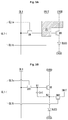
- FIGS. 6 and 7 are views for explaining an organic electroluminescent display device according to a first aspect of the present disclosure.
- the organic electroluminescent display device is implemented based on a white light emitting diode having two stacks of light emitting layers.
- the white light emitting diode having two stacks may be implemented as a light emitting layer made of an organic material or a light emitting layer made of an inorganic material, but the light emitting layer made of the organic material will be described below as an example.
- the 2 stack white organic light emitting diode has a structure in which two light emitting layers EL 1 and EL 2 located at different layers emit white light by a positive voltage (+) an anode electrode Anode and a negative voltage ( ⁇ ) applied to a cathode electrode Cathode.
- VEL is a power source in FIG. 6 .
- the 2 stack white organic light emitting diode has a stack structure comprising the anode electrode Anode, a first light emitting layer EL 1 , a charge generating layer CGL, a second light emitting layer EL 2 and the cathode Cathode.
- the first and second light emitting layers EL 1 and EL 2 includes a common layer for controlling the injection and transport of electrons and holes as well as a light emitting layer for emitting light, respectively.
- the first and second light emitting layers EL 1 and EL 2 include materials for emitting light of different colors, but emit white light when they emit light.
- the first light emitting layer EL 1 may include a material for emitting blue color (B) and the second light emitting layer EL 2 may include a material for emitting yellowish green color (YG) (or yellow color).
- B blue color
- YG yellowish green color
- the 2 stack white organic light emitting diode according to the first aspect may be formed on an insulating layer having a flat surface such as a planarization layer PLL. Trenches (or grooves) are formed on the planarization layer PLL to form a certain depth and width and recessed from the surface. The trenches are formed in a large number to serve to define the region between the subpixels.
- a trench is formed in the form of a closed curve that surrounds all the periphery of a unit subpixel to define the area between respective subpixels.
- the 2 stack white organic light emitting diodes are formed separately for each subpixel by a plurality of trenches formed on the planarization layer PLL. Since the trenches are formed to separate the subpixels from the subpixels, so the trenches may have a shape such as a triangle, a rectangle, a rhombus, a polygon, a circle, an ellipse, etc. according to the shape of the subpixel, but are not limited thereto.
- the 2 stack white organic light emitting diode according to the first aspect comprise a first subpixel electrically connected to the charge generating layer CGL and the cathode electrode Cathode and a second subpixel which is not electrically connected to the charge generating layer CGL and the cathode electrode Cathode.
- the charge generating layer CGL may comprise a conductive material such as lithium Li and calcium Ca which may cause an electrical short to the cathode electrode Cathode, but is not limited thereto.
- the second light emitting layer EL 2 does not emit light and only the first light emitting layer EL 1 emits light.
- both the first and second light emitting layers EL 1 and EL 2 emit light. That is, the first subpixel emits blue light and the second subpixel emits both of the blue light and yellowish green light, thereby emitting white light.
- the trench serves to define the region between the subpixels, as well as to help contact or separation between the layers at a specific location.
- the first subpixel and the second subpixel described above are distinguished by adjusting the width of at least one of the plurality of trenches.
- the width of the trench distinguishes between the first and second subpixels and also corresponds to a factor that determines structural characteristics, such as whether to provide a structure to assist or separate the contact between layers at a particular location.
- the first subpixel has a first trench of a first width (wide width) for contact between the charge generating layer CGL and the cathode electrode Cathode, while the second subpixel has a second trench of a second width (narrow width) for non-contact between the charge generating layer CGL and the cathode electrode Cathode. That is, the first and second trenches have different widths.
- first trench it is described that the first trench is included in the first subpixel because it also serves to assist the contact between the charge generating layer CGL and the cathode electrode Cathode in addition to defining the region between the subpixels.
- first and second trenches may be disposed together between two subpixels positioned at a first location, and only a first trench or only a second trench may be disposed between two subpixels positioned at a second location.
- FIG. 7 shows a portion of a trench having a wide width. Referring to the portion, it can be clearly seen how the charge generating layer CGL and the cathode electrode Cathode are electrically connected. The description with reference to FIG. 7 is added as follows.
- the first light emitting layer EL 1 is formed through a deposition process preceding the charge generating layer CGL and the second light emitting layer EL 2 . So, the first light emitting layer EL 1 is deposited while digging along a wide width of the trench and at this time the width of the trench is significantly narrowed.
- the charge generating layer CGL and the second light emitting layer EL 2 are formed through deposition processes following the first light emitting layer EL 1 . So, the charge generating layer CGL and the second light emitting layer EL 2 cannot penetrate into the interior of the trench and are deposited only on an exposed upper surface of the first light emitting layer EL 1 .
- the charge generating layer CGL and the second light emitting layer EL 2 form a profile in which the left and right sides are separated from each other around the trench as shown in the figure. And, as the left and right sides are separated, the side surfaces as well as the upper surfaces of the charge generating layer CGL and the second light emitting layer EL 2 become exposed. The side surfaces of the charge generating layer CGL and the second light emitting layer EL 2 are exposed inside the trench.
- the cathode electrode Cathode is deposited on the exposed upper surfaces of the second light emitting layer EL 2 and also on the side surfaces of the first light emitting layer EL 1 existing inside the trench, while penetrating into the interior of the trench.
- the trench having a wide width provides a contacting structure (side contacting structure) which causes an electrical short between the cathode electrode Cathode and the charge generating layer CGL.
- the charge generating layer CGL and the second light emitting layer EL 2 form a profile in which a right side and a left side are separated around the trench.
- the cathode electrode Cathode cannot penetrate into the inside of the trench and is deposited only on an exposed upper surface of the second light emitting layer EL 2 . The reason for this is briefly explained as follows.
- a trench having a narrow width provides a limited space to the inside of which only a part of the first light-emitting layer EL 1 can penetrate. Therefore, the space formed by the trench having a narrow width is closed simultaneously with the deposition of the second light emitting layer EL 2 which is thicker than the charge generating layer CGL. As a result, the trench having a narrow width provides a non-contact structure which does not cause an electrical short between the cathode electrode Cathode and the charge generating layer CGL.
- subpixels when at least two trenches of different sizes are formed, it is possible to form subpixels based on 2 stack organic white light emitting diodes by one deposition. And, subpixels may be divided into a first subpixel emitting blue light and a second subpixel emitting white light. That is, the first aspect can manufacture, by one deposition, a display panel having a two-color sub-pixel structure in which two or more colors including blue color and white color are emitted, so is advantageous in terms of process cost reduction and material cost reduction.
- the 2 stack white organic light emitting diode has a same laminated structure as the first aspect, but due to the trenches having different widths, one emits light in a single stack form and the other emits light in a double stack form.
- FIG. 8 is a view for explaining an organic electroluminescent display device according to a second aspect of the present disclosure.
- the display panel of an organic electroluminescent display device is also implemented based on the 2 stack white organic light emitting diode described above in the first aspect.
- the display panel includes a first substrate 110 a and a second substrate 110 b .
- the first substrate 110 a is made of glass or resin.
- the second substrate 110 b is a multi-layer thin film or a film and may include a first layer 120 and a second layer 130 which are alternately deposited with organic and inorganic materials.
- Color filter layers CFR, CFG and CFB are positioned on the second substrate 110 b .
- the color filter layers CFR, CFG and CFB performs a function of converting a white light output through the second substrate 110 b into a red light R, a green light G and a blue light B.
- the color filter layers CFR, CFG and CFB are arranged at sizes corresponding to the regions of the subpixels SPR, SPG and SPB.
- the types of colors that can be converted into by the color filter layers CFR, CFG and CFB are not limited to these.
- the planarization layer PLL is positioned on the first substrate 110 a .
- the planarization layer PLL has a predetermined thickness and performs a function of flattening the surface of the first substrate 110 a .
- the planarization layer PLL may be formed of organic materials such as a negative overcoat layer, polyimide, benzocyclobutene series resin, acrylate, photoacrylate, and the like, but is not limited thereto.
- a lower electrode layer E 1 is positioned on the planarization layer PLL.
- the lower electrode layer E 1 becomes an anode electrode or a cathode electrode.
- the lower electrode layer E 1 when the lower electrode layer E 1 is selected as the anode electrode, it may be made of oxides such as indium tin oxide ITO or indium zinc oxide IZO, but is not limited thereto.
- a bank layer BNK is positioned on the planarization layer PLL.
- the bank layer BNK exposes a part of the lower electrode layer E 1 while covering the lower electrode layer E 1 .
- the bank layer BNK performs a function of defining an emitting area of a subpixel.
- the bank layer BNK may be made of organic materials such as polyimide, benzocyclobutene series resin, acrylate, photoacrylate, and the like, but is not limited thereto.
- a first emitting layer EL 1 is positioned on the upper electrode layer E 1 .
- the first emitting layer EL 1 emits light of a first color.
- the first emitting layer EL 1 is defined as a first stack.
- the first emitting layer EL 1 includes a light emitting layer for emitting light and a common layer for controlling the injection and transport of electrons and holes.
- a charge generating layer CGL is positioned on the lower electrode layer E 1 .
- the charge generating layer CGL may be formed in the form of a PN junction in which an N-type charge generating layer and a P-type charge generating layer are bonded or a NP junction of vice versa.
- the charge generating layer CGL serves to generate charges or separate holes and electrons and inject charges into layers which are separated into a first stack and a second stack.
- An N-type charge generating layer provides electrons to the first emitting layer EL 1 and a P-type charge generating layer provides holes to the second emitting layer EL 2 , which may function to further lower a driving voltage of a device having a plurality of light emitting layers while further increasing the luminous efficiency of the device.
- the N-type charge generating layer is made of a metal or an organic material doped with an N-type.
- the metal may be a material selected from the group consisting of Li, Na, K, Rb, Cs, Mg, Ca, Sr, Ba, La, Ce, Sm, Eu, Tb, Dy and Yb.
- An N-type dopant used for the organic material doped with the N-type and a material of a host may be materials conventionally used.
- the N-type dopant may be an alkali metal, an alkali metal compound, an alkaline earth metal or an alkaline earth metal compound.
- the N-type dopant may be selected from the group consisting of Cs, K, Rb, Mg, Na, Ca, Sr, Eu and Yb.
- the host may be a material selected from the group consisting of tris (8-hydroxyquinoline) aluminum, triazine, hydroxyquinoline derivatives, benzazole derivatives and silole derivatives.
- the P-type charge generating layer is made of a metal or an organic material doped with a P-type.
- the metal may be composed of one or more alloys selected from the group consisting of Al, Cu, Fe, Pb, Zn, Au, Pt, W, In, Mo, Ni and Ti.
- a P-type dopant used for the organic material doped with the P-type and a material of a host may be materials conventionally used.
- the P-type dopant may be selected from the group consisting of 2,3,5,6-tetrafluoro-7,7,8,8-tetracyanoquinodimethane (F4-TCNQ), derivatives of tetracyanoquinodimethane, iodine, FeCl3, FeF3 and SbCl5.
- F4-TCNQ 2,3,5,6-tetrafluoro-7,7,8,8-tetracyanoquinodimethane
- derivatives of tetracyanoquinodimethane iodine
- FeCl3, FeF3 FeF3
- SbCl5 2,3,5,6-tetrafluoro-7,7,8,8-tetracyanoquinodimethane
- the host may be selected from the group consisting of N,N′-di(naphthalene-1-yl)-N,N-diphenyl-benzidine(NPB), N,N-diphenyl-N,N′-bis(3-methylphenyl)-1,1-biphenyl-4,4′-diamine(TPD) and N,N′,N′-tetranaphthyl-benzidine(TNB).
- NPB N,N′-di(naphthalene-1-yl)-N,N-diphenyl-benzidine
- TPD N,N-diphenyl-N,N′-bis(3-methylphenyl)-1,1-biphenyl-4,4′-diamine
- TPD N,N′,N′-tetranaphthyl-benzidine
- the second emitting layer EL 2 is positioned on the charge generating layer CGL.
- the second emitting layer EL 2 emits light of a second color different from the first color.
- the second emitting layer EL 2 is defined as a second stack.
- the second emitting layer EL 2 includes a light emitting layer for emitting light and a common layer for controlling the injection and transport of electrons and holes.
- An upper electrode layer E 2 is positioned on the second emitting layer EL 2 .
- the upper electrode layer E 2 becomes a cathode electrode or an anode electrode.
- the upper electrode layer E 2 may be made of, but not limited to, aluminum (Al), magnesium (Mg), silver (Ag) or an alloy thereof having a low work function.
- the 2 stack white organic light emitting diode OLED is formed on the planarization layer PLL.
- a plurality of first trenches TRH 1 and second trenches TRH 2 which have a predetermined depth and width and are recessed from a surface, are formed on the planarization layer PLL.
- the first trench TRH 1 and the second trench TRH 2 have different sizes to perform different functions.
- the first trench TRH 1 serves to define an area between subpixels SPB, SPR and SPG.
- the 2 stack white organic light emitting diode OLED is formed separately for each of the subpixels SPB, SPR and SPG on the planarization layer PLL.
- the first trench TRH 1 serves to help an electrical contact between the charge generating layer CGL and the upper electrode layer EL 2 as well as to define an area between the subpixels SPB, SPR and SPG.
- the second trench TRH 2 serves to help an electrical separation between the charge generating layer CGL and the upper electrode layer EL 2 .
- the first trench TRH 1 has a wider width than the second trench TRH 2
- the second trench TRH 2 has a narrower width than the first trench TRH 1 .
- the 2 stack white organic light emitting diode is formed based on the trenches TRH 1 and TRH 2 of the above-described structure, so has a first subpixel in which the charge generating layer CGL and the upper electrode layer EL 2 are electrically connected and a second subpixel in which the charge generating layer CGL and the upper electrode layer EL 2 are not electrically connected.
- the first subpixel may include a blue subpixel SPB having a blue color filter layer CFB and the first trench TRH 1 in the “CGL & EL 2 contact” portion. Since the charge generating layer CGL is electrically connected to the upper electrode layer EL 2 , only the first emitting layer EL 1 emits light in the first subpixel. A blue light emitted from the first emitting layer EL 1 is output through the blue color filter layer CFB.
- the second subpixel may include a red subpixel SPR having a red color filter layer CFR, the first trench TRH 1 and the second trench TRH 2 and a green subpixel SPG having a green color filter layer CFG, the first trench TRH 1 and the second trench TRH 2 in the “CGL & EL 2 non-contact” portion. Since the charge generating layer CGL is not electrically connected to the upper electrode layer EL 2 , both of the first emitting layer EL 1 and the second emitting layer EL 2 emit light in the second subpixel. A white light emitted from the first and second emitting layers EL 1 and EL 2 is output through the red color filter layer CFR and the green color filter layer CFG, respectively.
- the second aspect has (1) a driving voltage reduction effect in terms of individual elements and (2) a power saving effect in terms of a display panel, because it has the first subpixel which is driven only by a single stack.
- the first sub-pixel driven only by the single stack has the effect of outputting a higher luminance (brightness enhancement) even when a same voltage as the second subpixel is applied.
- a display panel capable of expressing various colors can be manufactured based on a two-color subpixel structure that emits two or more colors of a blue subpixel and a white subpixel, so there are advantages of reducing a process cost and a material cost.
- a two color emitting display panel can be manufactured which drive a predetermined subpixel such as a blue subpixel in the form of a single stack but not two stacks, so there are advantages of lowering a driving voltage, reducing a power consumption and increasing luminance.
- FIGS. 9A, 9B and 10 are views for explaining an organic electroluminescent display device according to a third aspect of the present disclosure.
- a display panel of an organic electroluminescent display device is also implemented based on the 2 stack white organic light emitting diode described in the second aspect.
- subpixels SPR, SPG and SPB such as FIG. 9A or subpixels SPR, SPG and SPB such as FIG. 9B may be designed, which will be described as follows by referring to FIGS. 9A, 9B and 10 .
- a blue color filter layer CFB which is requested in a blue subpixel SPB belonging to a first subpixel can be deleted (omitted or not included).
- the reason is that only a first emitting layer EL 1 which emits light of a blue color B in the first subpixel emits light, as described above in the second aspect.
- the third aspect omits only a portion corresponding to the blue color filter layer CFB when forming a color filter layer, a material cost can be reduced. And, since the blue light emitted from the first light emitting layer EL 1 is emitted without being converted through the blue color filter layer CFB, there is an advantage that an emitting efficiency and a luminance can be simultaneously increased.
- the condition such as “SPG ⁇ SPR ⁇ SPB” may be applied as FIG. 9A
- the condition such as “SPG ⁇ SPR ⁇ SPB” may be applied as FIG. 9B
- the third aspect can manufacture the display panel which can represent various colors based on the two-color subpixel structure which emits two or more colors, so it has advantages in process cost reduction and material cost reduction. And, third aspect can manufacture two-color emitting display panel which drives a predetermined subpixel such as the blue subpixel in a single stack form instead of two stacks, which is advantageous in lowering a driving voltage and reducing power consumption. Also, the third aspect is advantageous in that the blue color filter layer can be eliminated in forming the color filter layer, thereby improving an emitting efficiency and a luminance, and reducing a material cost.
- FIGS. 11 to 13 are views for explaining an organic electroluminescent display device according to a fourth aspect of the present disclosure
- FIGS. 14 to 16 are views for explaining a modification of the fourth aspect of the present disclosure.
- a display panel of an organic electroluminescent display device is also implemented based on the 2 stack white organic light emitting diode described in the second aspect.
- the display panel 110 includes a first substrate 110 a and a second substrate 110 b .
- the first and second substrate 110 a and 110 b are made of glass, resin or a film.
- a transistor portion TFTA, a two stack white organic light emitting diode OLED and a color filter layer CF are disposed between the first substrate 110 a and the second substrate 110 b .
- the transistor portion TFTA includes a switching transistor, a driving transistor, and the like.
- the transistor portion TFTA has various structures depending on a manufacturing method of the transistors, and is not specifically shown.
- the 2 stack white organic light emitting diode OLED further includes metal layers TFTC, CNT, ADM and REM for helping an electrical connection with the transistor portion TFTA and helping the light generated from the emitting layers EL 1 and EL 2 to emit upward.
- metal layers TFTC, CNT, ADM and REM described below may be eliminated or integrated depending on the manufacturing method of the device.
- a first metal layer TFTC is positioned on the transistor portion TFTA.
- the first metal layer TFTC may become a source electrode layer or a drain electrode layer included in a driving transistor or may be selected as a separate metal layer connected to the source electrode layer or the drain electrode layer.
- the first metal layer TFTC serves as an electrode contact metal layer to facilitate an electrical connection between the source or drain electrode of the driving transistor and the lower electrode layer E 1 .
- a second metal layer CNT is positioned to penetrate the planarization layer PLL.
- the second metal layer CNT is electrically connected to the first metal layer TFTC exposed under the planarization layer PLL.
- the second metal layer CNT also serves as the electrode contact metal layer to facilitate the electrical connection between the source or drain electrode of the driving transistor and the lower electrode layer E 1 together with the first metal layer TFTC.
- a third metal layer ADM is positioned on the planarization layer PLL.
- the third metal layer ADM is electrically connected to the second metal layer CNT penetrating the planarization layer PLL.
- the third metal layer ADM and the second metal layer CNT may be integrally formed, but may be formed separately as shown in FIG. 12 .
- the third metal layer ADM serves to increase an adhesive force at a surface of the planarization layer PLL and serves as the electrode contact metal layer to facilitate the electrical connection between the source or drain electrode of the driving transistor and the lower electrode layer E 1 together with the first and second metal layers TFTC and CNT.
- a fourth metal layer REM is positioned on and electrically connected to the third metal layer ADM.
- the fourth metal layer REM serves as a reflecting layer to help the light generated from the emitting layers EL 1 and EL 2 to emit upward.
- the fourth metal layer REM serves as the electrode contact metal layer to facilitate the electrical connection between the source or drain electrode of the driving transistor and the lower electrode layer E 1 together with the first to third metal layers TFTC, CNT and ADM.
- the 2 stack white organic light emitting diode is formed based on trenches TRH 1 and TRH 2 of a same structure as the second aspect, so comprises a first subpixel in which the charge generating layer and the upper electrode layer EL 2 are electrically connected and a second subpixel in which the charge generating layer and the upper electrode layer EL 2 are not electrically connected.
- the first subpixel may include an A subpixel SPA having a first trench TRH 1 in the “CGL & EL 2 contact” portion. Since the charge generating layer and the upper electrode layer EL 2 are electrically connected in the first subpixel, only the first emitting layer EL 1 emits light.
- the second subpixel may include a B subpixel SPB having the first trench TRH 1 and a second trench TRH 2 and a C subpixel SPC having the first and second trenches TRH 1 and TRH 2 in the “CGL & EL 2 Non-contact” portion. Since the charge generating layer and the upper electrode layer EL 2 are not electrically connected in the second subpixel, both of the first and second emitting layers EL 1 and EL 2 emit light.
- Color filter layers are not shown in FIG. 12 . This is because a color filter layer may be located above the second substrate 110 b as well as between the second substrate 110 b and the upper electrode layer E 1 as in the second aspect.
- FIG. 12 adds an enlarged view of a structure related to the first trench TRH 1 and the second trench TRH 2 .
- FIG. 13 shows an enlarged image related to a profile in which left and right structures are separated around a narrow second trench TRH 2 .
- trenches TRH 1 and TRH 2 may be electrically contacted to or separated from the charge generating layer CGL depending on sizes of widths of the trench. And, according to this characteristic, subpixels based on the 2 stack white organic light emitting diode may be formed with a single deposition. Thus, since the width and depth of the structure such as the first trench of FIG. 7 Trench and the second trench of FIG. 13 TRH 2 may be factors determining a profile of organic layers, so they are optimized through repeated experiments.
- a display panel such as FIG. 14 which has all of the first to third color filter layers CFA, CFB and CFC on an upper surface of the second substrate 110 b (or a lower surface of the second substrate) can be manufactured.
- a display panel such as FIG. 15 which has only the second and third color filter layers CFB and CFC without the first color filter layer CFA on an upper surface of the second substrate 110 b (or a lower surface of the second substrate) can be manufactured.
- a display panel may represent a white color by blending three primary colors of red R, green G and blue B or blending colors such as purple red (Magenta), cyan (Cyan), and yellowish green YG (or yellow).
- the first and second emitting layers EL 1 and EL 2 may respectively emits a blue color Blue and a yellowish green color YG or may be implemented like the combinations shown in FIG. 16B .
- a display panel may represent a white color by using the first and second emitting layers EL 1 and EL 2 based on red, green and blue filter layers, or based on purple red, cyan and yellowish green filter layers. Examples for this are as follows.
- the first emitting layer EL 1 may emit a blue color Blue and the second emitting layer EL 2 may emit a yellowish green color YG.
- a blue color filter layer (Blue CF) can be omitted.
- the first and second emitting layers EL 1 and EL 2 may respectively emit a green color Green and a purple red color Magenta.
- a green color filter layer (Green CF) can be omitted.
- the first and second emitting layers EL 1 and EL 2 may respectively emit a red color Red and a cyan color Cyan, and in this case a red color filter layer (Red CF) can be omitted.
- the first and second emitting layers EL 1 and EL 2 may respectively emit a yellowish green color YG and a blue color Blue, and in this case a yellowish green color filter layer or a yellow color filter (Y CF) can be omitted.
- the first and second emitting layers EL 1 and EL 2 may respectively emit a purple red color Magenta and a green color Green, and in this case a purple red color filter layer (M CF) can be omitted.
- the first and second emitting layers EL 1 and EL 2 may respectively emit a cyan color Cyan and a red color Red, and in this case a cyan color filter layer (C CF) can be omitted.
- the fourth aspect can manufacture a display panel which can represent various colors based on the 2 color subpixel structure including a blue subpixel and a white subpixel to emit two or more colors, thereby reducing a process cost and a material cost.
- the fourth aspect can manufacture a two-color emitting display panel which drives a predetermined subpixel such as a blue subpixel in a single stack form instead of two stacks, which is advantageous in lowering a driving voltage and reducing power consumption.
- the fourth aspect is advantageous in that the blue color filter layer can be eliminated in forming the color filter layer, thereby improving an emitting efficiency and a luminance and reducing a material cost.
- the fourth aspect can add a metal layer which reflects light generated from the emitting layers as well as electrically connects electrodes located on different layers, which is advantageous in enhancing an ability to emit light.
- a display panel capable of representing various colors can be manufactured based on a two-color subpixel structure that emits two colors of a blue subpixel and a white subpixel. Also, the present disclosure has the effect of lowering a driving voltage, reducing power consumption, improving luminous efficiency and luminance, reducing a material cost, and improving light output capability based on a subpixel structure emitting at least two colors.
Landscapes
- Physics & Mathematics (AREA)
- Optics & Photonics (AREA)
- Engineering & Computer Science (AREA)
- Microelectronics & Electronic Packaging (AREA)
- Geometry (AREA)
- Electroluminescent Light Sources (AREA)
Abstract
Description
Claims (13)
Applications Claiming Priority (2)
| Application Number | Priority Date | Filing Date | Title |
|---|---|---|---|
| KR1020170145880A KR102511045B1 (en) | 2017-11-03 | 2017-11-03 | Light Emitting Display Device |
| KR10-2017-0145880 | 2017-11-03 |
Publications (2)
| Publication Number | Publication Date |
|---|---|
| US20190181368A1 US20190181368A1 (en) | 2019-06-13 |
| US10693099B2 true US10693099B2 (en) | 2020-06-23 |
Family
ID=66401440
Family Applications (1)
| Application Number | Title | Priority Date | Filing Date |
|---|---|---|---|
| US16/178,743 Active US10693099B2 (en) | 2017-11-03 | 2018-11-02 | Electroluminescent display device having a charge generating layer between a plurality of light emitting layers |
Country Status (3)
| Country | Link |
|---|---|
| US (1) | US10693099B2 (en) |
| KR (1) | KR102511045B1 (en) |
| CN (1) | CN109755396B (en) |
Families Citing this family (10)
| Publication number | Priority date | Publication date | Assignee | Title |
|---|---|---|---|---|
| KR102640476B1 (en) * | 2019-08-13 | 2024-02-23 | 엘지디스플레이 주식회사 | Display device and method for manufacturing the same |
| KR102687966B1 (en) | 2019-12-30 | 2024-07-23 | 엘지디스플레이 주식회사 | Display device |
| JP2021179491A (en) * | 2020-05-12 | 2021-11-18 | セイコーエプソン株式会社 | Electrooptical device and electronic apparatus |
| KR102860230B1 (en) * | 2020-12-22 | 2025-09-15 | 엘지디스플레이 주식회사 | Electroluminescent Display Device |
| KR20220096855A (en) * | 2020-12-31 | 2022-07-07 | 엘지디스플레이 주식회사 | Display apparatus |
| US20240155871A1 (en) * | 2021-03-11 | 2024-05-09 | Semiconductor Energy Laboratory Co., Ltd. | Display Device |
| US20240172487A1 (en) * | 2021-03-11 | 2024-05-23 | Semiconductor Energy Laboratory Co., Ltd. | Display apparatus and manufacturing method of the display apparatus |
| KR102883150B1 (en) | 2021-07-28 | 2025-11-07 | 삼성디스플레이 주식회사 | Display device and method for manufacturing display device |
| CN113823754B (en) * | 2021-10-22 | 2025-03-11 | 京东方科技集团股份有限公司 | Display substrate and preparation method thereof, and display device |
| CN116828914A (en) * | 2023-08-03 | 2023-09-29 | 京东方科技集团股份有限公司 | Array substrate and manufacturing method thereof, display panel and display device |
Citations (5)
| Publication number | Priority date | Publication date | Assignee | Title |
|---|---|---|---|---|
| KR20150025727A (en) | 2013-08-30 | 2015-03-11 | 엘지디스플레이 주식회사 | White organic light emitting diode and display device using the same |
| KR20170051614A (en) | 2015-10-29 | 2017-05-12 | 삼성디스플레이 주식회사 | Display device and fabrication method of the same |
| KR20170064164A (en) | 2015-11-30 | 2017-06-09 | 엘지디스플레이 주식회사 | Organic light emitting diode display device |
| US20180122870A1 (en) * | 2016-10-31 | 2018-05-03 | Lg Display Co., Ltd. | Organic light-emitting device and organic light-emitting display device using the same |
| US10340315B2 (en) * | 2016-05-25 | 2019-07-02 | Samsung Display Co., Ltd. | Organic light emitting display with color filter layers |
Family Cites Families (8)
| Publication number | Priority date | Publication date | Assignee | Title |
|---|---|---|---|---|
| US7242398B2 (en) * | 2002-02-18 | 2007-07-10 | Ignis Innovation Inc. | Flexible display device |
| JP4610408B2 (en) * | 2004-04-28 | 2011-01-12 | 株式会社半導体エネルギー研究所 | LIGHT EMITTING ELEMENT, ITS MANUFACTURING METHOD, AND LIGHT EMITTING DEVICE |
| JP5708152B2 (en) * | 2011-03-31 | 2015-04-30 | ソニー株式会社 | Display device and manufacturing method thereof |
| US8921842B2 (en) * | 2012-11-14 | 2014-12-30 | Lg Display Co., Ltd. | Organic light emitting display device and method of manufacturing the same |
| KR101622913B1 (en) * | 2012-11-14 | 2016-05-20 | 엘지디스플레이 주식회사 | Organic Light Emitting Display Device and fabricating of the same |
| JP6465545B2 (en) * | 2013-09-27 | 2019-02-06 | ソニー株式会社 | Imaging device, manufacturing method thereof, and electronic apparatus |
| KR102377466B1 (en) * | 2015-10-29 | 2022-03-21 | 엘지디스플레이 주식회사 | Organic light emitting display apparatus |
| CN107170779A (en) * | 2017-05-12 | 2017-09-15 | 京东方科技集团股份有限公司 | A kind of oled display substrate and display device |
-
2017
- 2017-11-03 KR KR1020170145880A patent/KR102511045B1/en active Active
-
2018
- 2018-11-02 CN CN201811299595.XA patent/CN109755396B/en active Active
- 2018-11-02 US US16/178,743 patent/US10693099B2/en active Active
Patent Citations (5)
| Publication number | Priority date | Publication date | Assignee | Title |
|---|---|---|---|---|
| KR20150025727A (en) | 2013-08-30 | 2015-03-11 | 엘지디스플레이 주식회사 | White organic light emitting diode and display device using the same |
| KR20170051614A (en) | 2015-10-29 | 2017-05-12 | 삼성디스플레이 주식회사 | Display device and fabrication method of the same |
| KR20170064164A (en) | 2015-11-30 | 2017-06-09 | 엘지디스플레이 주식회사 | Organic light emitting diode display device |
| US10340315B2 (en) * | 2016-05-25 | 2019-07-02 | Samsung Display Co., Ltd. | Organic light emitting display with color filter layers |
| US20180122870A1 (en) * | 2016-10-31 | 2018-05-03 | Lg Display Co., Ltd. | Organic light-emitting device and organic light-emitting display device using the same |
Also Published As
| Publication number | Publication date |
|---|---|
| CN109755396A (en) | 2019-05-14 |
| CN109755396B (en) | 2021-10-15 |
| KR20190050460A (en) | 2019-05-13 |
| KR102511045B1 (en) | 2023-03-16 |
| US20190181368A1 (en) | 2019-06-13 |
Similar Documents
| Publication | Publication Date | Title |
|---|---|---|
| US10693099B2 (en) | Electroluminescent display device having a charge generating layer between a plurality of light emitting layers | |
| US12347385B2 (en) | Display substrate and display device | |
| CN109860230B (en) | Luminous display device | |
| KR102011952B1 (en) | Light Emitting Display Device and Manufacturing Method of the same | |
| US11063096B2 (en) | Organic light emitting diode display device | |
| CN109979963B (en) | Display device and electroluminescent display | |
| CN105742323B (en) | Organic Light Emitting Diode Display with Multilayer Stacked Structure | |
| KR101736929B1 (en) | White organic light emitting diode display device | |
| CN106935625B (en) | Organic Light Emitting Display | |
| US20230030891A1 (en) | Display substrate and display device | |
| CN102956666A (en) | Organic electroluminescence display device | |
| KR101878328B1 (en) | Organic electroluminescent Device | |
| KR101182268B1 (en) | Organic light emitting device | |
| KR102569690B1 (en) | Light Emitting Display Device | |
| KR101845309B1 (en) | Organic electro-luminescent Device | |
| CN106920816A (en) | Organic light emitting display device and organic light emitting stack structure | |
| KR20240035079A (en) | Display device including oxide semiconductor pattern | |
| KR20250131665A (en) | Light Emitting Display Device | |
| KR20250103191A (en) | Display device | |
| CN117460274A (en) | Display device | |
| KR20210016725A (en) | Organic electroluminescent display device |
Legal Events
| Date | Code | Title | Description |
|---|---|---|---|
| AS | Assignment |
Owner name: LG DISPLAY CO., LTD., KOREA, REPUBLIC OF Free format text: ASSIGNMENT OF ASSIGNORS INTEREST;ASSIGNORS:KIM, HOJIN;JUNG, GOEUN;BAIK, SEUNGMIN;REEL/FRAME:047391/0287 Effective date: 20181016 |
|
| FEPP | Fee payment procedure |
Free format text: ENTITY STATUS SET TO UNDISCOUNTED (ORIGINAL EVENT CODE: BIG.); ENTITY STATUS OF PATENT OWNER: LARGE ENTITY |
|
| STPP | Information on status: patent application and granting procedure in general |
Free format text: DOCKETED NEW CASE - READY FOR EXAMINATION |
|
| STPP | Information on status: patent application and granting procedure in general |
Free format text: NON FINAL ACTION MAILED |
|
| STPP | Information on status: patent application and granting procedure in general |
Free format text: NOTICE OF ALLOWANCE MAILED -- APPLICATION RECEIVED IN OFFICE OF PUBLICATIONS |
|
| STPP | Information on status: patent application and granting procedure in general |
Free format text: PUBLICATIONS -- ISSUE FEE PAYMENT VERIFIED |
|
| STCF | Information on status: patent grant |
Free format text: PATENTED CASE |
|
| MAFP | Maintenance fee payment |
Free format text: PAYMENT OF MAINTENANCE FEE, 4TH YEAR, LARGE ENTITY (ORIGINAL EVENT CODE: M1551); ENTITY STATUS OF PATENT OWNER: LARGE ENTITY Year of fee payment: 4 |