US10693048B2 - Flip-chip SMT LEDs with variable number of emitting surfaces - Google Patents
Flip-chip SMT LEDs with variable number of emitting surfaces Download PDFInfo
- Publication number
- US10693048B2 US10693048B2 US15/765,678 US201615765678A US10693048B2 US 10693048 B2 US10693048 B2 US 10693048B2 US 201615765678 A US201615765678 A US 201615765678A US 10693048 B2 US10693048 B2 US 10693048B2
- Authority
- US
- United States
- Prior art keywords
- leds
- led
- transparent spacer
- layer
- reflective layer
- Prior art date
- Legal status (The legal status is an assumption and is not a legal conclusion. Google has not performed a legal analysis and makes no representation as to the accuracy of the status listed.)
- Active
Links
Images


Classifications
-
- H01L33/60—
-
- H—ELECTRICITY
- H10—SEMICONDUCTOR DEVICES; ELECTRIC SOLID-STATE DEVICES NOT OTHERWISE PROVIDED FOR
- H10H—INORGANIC LIGHT-EMITTING SEMICONDUCTOR DEVICES HAVING POTENTIAL BARRIERS
- H10H20/00—Individual inorganic light-emitting semiconductor devices having potential barriers, e.g. light-emitting diodes [LED]
- H10H20/80—Constructional details
- H10H20/85—Packages
- H10H20/8506—Containers
-
- H01L33/486—
-
- H01L33/50—
-
- H01L33/52—
-
- H—ELECTRICITY
- H10—SEMICONDUCTOR DEVICES; ELECTRIC SOLID-STATE DEVICES NOT OTHERWISE PROVIDED FOR
- H10H—INORGANIC LIGHT-EMITTING SEMICONDUCTOR DEVICES HAVING POTENTIAL BARRIERS
- H10H20/00—Individual inorganic light-emitting semiconductor devices having potential barriers, e.g. light-emitting diodes [LED]
- H10H20/01—Manufacture or treatment
-
- H—ELECTRICITY
- H10—SEMICONDUCTOR DEVICES; ELECTRIC SOLID-STATE DEVICES NOT OTHERWISE PROVIDED FOR
- H10H—INORGANIC LIGHT-EMITTING SEMICONDUCTOR DEVICES HAVING POTENTIAL BARRIERS
- H10H20/00—Individual inorganic light-emitting semiconductor devices having potential barriers, e.g. light-emitting diodes [LED]
- H10H20/80—Constructional details
- H10H20/85—Packages
- H10H20/851—Wavelength conversion means
-
- H—ELECTRICITY
- H10—SEMICONDUCTOR DEVICES; ELECTRIC SOLID-STATE DEVICES NOT OTHERWISE PROVIDED FOR
- H10H—INORGANIC LIGHT-EMITTING SEMICONDUCTOR DEVICES HAVING POTENTIAL BARRIERS
- H10H20/00—Individual inorganic light-emitting semiconductor devices having potential barriers, e.g. light-emitting diodes [LED]
- H10H20/80—Constructional details
- H10H20/85—Packages
- H10H20/852—Encapsulations
-
- H—ELECTRICITY
- H10—SEMICONDUCTOR DEVICES; ELECTRIC SOLID-STATE DEVICES NOT OTHERWISE PROVIDED FOR
- H10H—INORGANIC LIGHT-EMITTING SEMICONDUCTOR DEVICES HAVING POTENTIAL BARRIERS
- H10H20/00—Individual inorganic light-emitting semiconductor devices having potential barriers, e.g. light-emitting diodes [LED]
- H10H20/80—Constructional details
- H10H20/85—Packages
- H10H20/855—Optical field-shaping means, e.g. lenses
- H10H20/856—Reflecting means
-
- H—ELECTRICITY
- H10—SEMICONDUCTOR DEVICES; ELECTRIC SOLID-STATE DEVICES NOT OTHERWISE PROVIDED FOR
- H10H—INORGANIC LIGHT-EMITTING SEMICONDUCTOR DEVICES HAVING POTENTIAL BARRIERS
- H10H29/00—Integrated devices, or assemblies of multiple devices, comprising at least one light-emitting semiconductor element covered by group H10H20/00
- H10H29/10—Integrated devices comprising at least one light-emitting semiconductor component covered by group H10H20/00
- H10H29/14—Integrated devices comprising at least one light-emitting semiconductor component covered by group H10H20/00 comprising multiple light-emitting semiconductor components
- H10H29/142—Two-dimensional arrangements, e.g. asymmetric LED layout
-
- H10P54/00—
-
- H01L2933/0058—
-
- H01L33/58—
-
- H—ELECTRICITY
- H10—SEMICONDUCTOR DEVICES; ELECTRIC SOLID-STATE DEVICES NOT OTHERWISE PROVIDED FOR
- H10H—INORGANIC LIGHT-EMITTING SEMICONDUCTOR DEVICES HAVING POTENTIAL BARRIERS
- H10H20/00—Individual inorganic light-emitting semiconductor devices having potential barriers, e.g. light-emitting diodes [LED]
- H10H20/01—Manufacture or treatment
- H10H20/036—Manufacture or treatment of packages
- H10H20/0363—Manufacture or treatment of packages of optical field-shaping means
-
- H—ELECTRICITY
- H10—SEMICONDUCTOR DEVICES; ELECTRIC SOLID-STATE DEVICES NOT OTHERWISE PROVIDED FOR
- H10H—INORGANIC LIGHT-EMITTING SEMICONDUCTOR DEVICES HAVING POTENTIAL BARRIERS
- H10H20/00—Individual inorganic light-emitting semiconductor devices having potential barriers, e.g. light-emitting diodes [LED]
- H10H20/80—Constructional details
- H10H20/85—Packages
- H10H20/855—Optical field-shaping means, e.g. lenses
Definitions
- the present disclosure relates to semiconductor light-emitting diodes (LEDs), and more particular to side-emitting surface-mount technology (SMT) LEDs.
- LEDs semiconductor light-emitting diodes
- SMT surface-mount technology
- N-sided emitters In illumination and display applications, it is desirable to uniformly illuminate a diffuser screen using the minimal number of LEDs. In these applications, side emission with reduced or suppressed top emission is preferred. However many LEDs are Lambertian emitters that emit light in an omnidirectional pattern. Thus what is needed is an LED packaging technique that transforms Lambertian emitters into LEDs with variable number of emitting surfaces (hereafter “N-sided emitters”) with enhanced lateral radiation pattern into specific azimuthal directions.
- a method to make light-emitting diode (LED) units includes arranging LEDs in a pattern, forming an optically transparent spacer layer over the LEDs, forming an optically reflective layer over the LEDs, and singulating the LEDs into LED units.
- the method may further include, after forming the optically transparent spacer layer and before singulating the LEDs, forming a secondary light-emitting layer that conforms to the LEDs, cutting the LEDs to form LED groups having a same arrangement, spacing the LED groups on a support, and forming the optically reflective layer in spaces between the LED groups.
- FIG. 1 illustrates a top view of a packaging process for making four-sided emitter packages in examples of the present disclosure
- FIGS. 2 and 3 respectively illustrate a side cross-sectional view and a top view of a four-sided emitter package of FIG. 1 in examples of the present disclosure
- FIGS. 4 and 5 illustrate a top view of a packaging process for making three-sided emitter packages in examples of the present disclosure
- FIGS. 6 and 7 respectively illustrate a side cross-sectional view and a top view of a three-sided emitter package of FIG. 5 in examples of the present disclosure
- FIGS. 8 and 9 illustrate a top view of a packaging process for making two-sided emitter packages in examples of the present disclosure
- FIGS. 10 and 11 respectively illustrate a side cross-sectional view and a top view of a two-sided emitter package of FIG. 9 in examples of the present disclosure
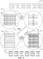
- FIGS. 12 and 13 illustrate a top view of a packaging process for making two-sided emitter packages in examples of the present disclosure
- FIGS. 14 and 15 respectively illustrate a side cross-sectional view and a top view of a two-sided emitter package of FIG. 13 in examples of the present disclosure
- FIG. 16 illustrates a top view of a packaging process for making single-sided emitter packages in examples of the present disclosure
- FIGS. 17 and 18 respectively illustrate a side cross-sectional view and a top view of a single-sided emitter package of FIG. 16 in examples of the present disclosure
- FIG. 19 illustrates a side cross-sectional view of a structure formed by an assembly process for integrating four or five-sided emitters on a printed circuit board in examples of the present disclosure.
- FIG. 20 is a flowchart of a method to make N-sided emitters in examples of the present disclosure.
- FIG. 1 illustrates a top view of a level-1 packaging process 100 for making light-emitting diode (LED) units or packages 101 (only one is labeled in view 120 ) in examples of the present disclosure.
- LED units 101 may be four-sided emitters that emit from four lateral surfaces.
- LEDs 104 are placed on a support 106 .
- LEDs 104 are surface-mount devices that can be mounted or placed directly onto the surface of interposers or printed circuit boards (PCBs).
- PCBs printed circuit boards
- Each LED 104 has a bottom contact surface and top and side-emitting surfaces.
- the bottom contact surface includes anode and cathode contacts 108 (shown in phantom).
- LED 104 may have an area of 0.1 millimeter (mm) by 0.1 mm to 10 by 10 mm2 and have a thickness from 10 microns ( ⁇ m) to 1 mm.
- LEDs 104 may be a flip-chip chip-scale package (CSP) LEDs.
- a pick-and-place machine picks up LEDs 104 from a tray or a reel and places them with their bottom contact surfaces facing down on support 106 .
- LEDs 104 are arranged in a pattern on support 106 , such as in a square or rectangular matrix 109 where neighboring LEDs 104 are spaced equally apart.
- Support 106 may be a tacky tape on a metal frame.
- one or more layers 112 , 114 , and 116 are formed over LEDs 104 on support 106 . Note that the use of the term “over” includes one element being directly atop another element.
- a secondary light-emitting layer 112 is formed over LEDs 104 on support 106 .
- Secondary light-emitting layer 112 also referred to as a wavelength converting layer, converts part of the primary light emitted by LEDs 104 to a secondary light of a different wavelength. The secondary light combines with the remainder of the primary light to produce a desired color.
- Secondary light-emitting layer 112 may be a laminate including a layer of titanium oxide (TiOx) (or another translucent or diffusive metal oxide) in silicone followed by a layer of phosphor in silicone.
- the layer of TiOx in silicone has a thickness of 10300 ⁇ m, and the phosphor in silicone layer has a thickness of 10-300 ⁇ m.
- a laminating machine may laminate secondary light-emitting layer 112 over and in-between LEDs 104 on support 106 .
- secondary light-emitting layer 112 is relatively thin, it conforms to the topography of LEDs 104 on support 106 .
- secondary light-emitting layer 112 is omitted when only the primary light is desired.
- An optically transparent spacer layer 114 is formed over secondary light-emitting layer 112 .
- transparent spacer layer 114 is formed over LEDs 104 on support 106 .
- Transparent spacer layer 114 encapsulates LEDs 104 and provides the proper spacing between LEDs 104 and a subsequent layer.
- Transparent spacer layer 114 may be silicone or glass.
- Transparent spacer layer 114 may have a thickness of 0 to 10 mm (e.g., 675 ⁇ m).
- a molding machine molds transparent spacer layer 114 over secondary light-emitting layer 112 or LEDs 104 and support 106 .
- Transparent spacer layer 114 has a completely planar top surface or a planar top surface with indentations, such as inverted cones or dimples, over LEDs 104 .
- An optically reflective layer 116 is formed over transparent spacer layer 110 .
- Reflective layer 116 prevents light from exiting through the top of LED units 101 .
- Reflective layer 116 may be TiOx (or another translucent or diffusive metal oxide) in silicone.
- Reflective layer 116 may have a thickness of 10 to 300 ⁇ m.
- a molding machine may mold a reflective layer 116 over transparent spacer layer 110 .
- Reflective layer 116 may be molded with a planar top surface. When transparent spacer layer 114 has inverted cones or dimples on its top surface, reflective layer 116 would fill in those indentations. At this point LEDs 104 are held together by one or more layers 112 , 114 , and 116 .
- LEDs 104 are flipped over by transferring them to a new support 119 so contacts 108 (only two are labeled) on their bottom contact surfaces are visible.
- the LEDs 104 are singulated along orthogonal scribe lanes 122 (only two are labeled) to form individual LED units 101 (only one is labeled).
- FIGS. 2 and 3 respectively illustrate a side cross-sectional view and a top view of LED unit 101 in examples of the present disclosure.
- LED unit 101 includes LED 104 , a secondary light emitter 112 - 1 over top and side-emitting surfaces of the LED, a transparent spacer 114 - 1 over the secondary light emitter, and a reflector 116 - 1 over a top surface of the transparent spacer.
- LED 104 typically has the shape of a rectangular prism but may be another shape such as a cube or a cylinder.
- Secondary light emitter 112 - 1 has the shape of a top hat with a crown that receives LED 104 and a brim that surrounds the base of the LED.
- Transparent spacer 114 - 1 has the shape of a cap with an opening that receives the crown of secondary light emitter 112 - 1 and a rim that sits on the brim of the secondary light emitter.
- Reflector 116 - 1 has the shape of a plate that sits over the top of transparent spacer 114 - 1 . As shown in FIG. 3 , LED unit 101 only emits light from its four lateral surfaces that are not covered by reflector 116 - 1 .
- FIGS. 4 and 5 illustrate a top view of a level-1 packaging process 400 for making LED units or packages 401 (only one is labeled in view 424 of FIG. 5 ) in examples of the present disclosure.
- LED units 401 may be three-sided emitters.
- FIG. 4 view 402 , LEDs 104 (only one is labeled) are placed with their bottom contact surfaces facing down on support 106 .
- LEDs 104 are placed in a pattern, such as in double rows 404 (only one is labeled) of the LEDs.
- Each double row 404 includes a first row of LEDs with their contact pads 108 in a first orientation, and a second row of LEDs with the contact pads 108 in a second orientation that is rotated 180 degrees from the first orientation.
- secondary light-emitting layer 112 is formed over LEDs 104 on support 106 , and optically transparent spacer layer 114 is formed over the secondary light-emitting layer.
- secondary light-emitting layer 112 is relatively thin, it conforms to the topography of LEDs 104 on support 106 .
- secondary light-emitting layer 112 is omitted and transparent spacer layer 114 is formed over LEDs 104 on support 106 .
- Transparent spacer layer 114 has a completely planar top surface or a substantially planar top surface with indentations, such as inverted cones or dimples, over LEDs 104 . At this point LEDs 104 are held together by secondary light-emitting layer 112 and transparent spacer layer 114 or the transparent spacer layer alone.
- LEDs 104 are flipped over by transferring them to a new support 410 so contacts 108 (only two are labeled) on the bottom contact surfaces of the LEDs are visible.
- Support 410 may be a tacky tape supported by a metal rim.
- LEDs 104 are cut into LED groups 414 having the same arrangement along horizontal scribe lanes 416 .
- Each LED groups 414 includes a double row 404 of LEDs 104 .
- LED groups 414 are spaced apart and then flipped over by transferring them to a new support 420 .
- Support 420 may be a tacky tape on a metal frame.
- optically reflective layer 116 is formed over and in-between LED groups 414 (not labeled). Reflective layer 116 prevents light from exiting through the top of LED units 401 . Reflective layer 116 may be molded with a planar top surface. When transparent spacer layer 114 of LED groups 412 has inverted cones or dimples on its top surface, reflective layer 116 would fill in those indentations. At this point LED groups 414 are held together by reflective layer 116 .
- LED groups 414 are flipped over by transferring them to a new support 119 so contacts 108 on the bottom contact surfaces of LEDs 104 are visible.
- LEDs 104 (only one is labeled) are singulated into individual LED units 401 (only one is labeled) along orthogonal scribe lanes 428 (only two are labeled).
- Vertical scribe lanes 428 between the ends cut between neighboring LEDs 104 Horizontal scribe lanes 428 cut through reflective layer 116 above and below LED groups 414 so portions of the reflective layer 116 remains on the top edge of the first row and the bottom edge of the second row in each LED group.
- FIGS. 6 and 7 respectively illustrate a side cross-sectional view and a top view of LED unit 401 in examples of the present disclosure.
- LED unit 401 includes LED 104 , secondary light emitter 112 - 1 , transparent spacer 114 - 1 , and a reflector 116 - 2 .
- Reflector 116 - 2 forms two plates that sit over the top of transparent spacer 114 - 1 and one side of the transparent spacer and the brim of secondary light emitter 112 - 1 .
- LED unit 401 emits light only from three side-emitting surfaces that are not covered by reflector 116 - 2 .
- FIGS. 8 and 9 illustrate a top view of a level-1 packaging process 800 for making LED units or packages 801 (only one is labeled in view 820 of FIG. 9 ) in examples of the present disclosure.
- LED units 801 may be two-sided emitters.
- FIG. 8 view 802 , LEDs 104 (only one is labeled) are placed with their bottom contact surfaces facing down on support 106 . LEDs 104 are placed in a pattern, such as in two-by-two arrays 804 (only one is labeled).
- Each two-by-two array 804 includes, in a spiral order, a first LED with its contact pads 108 in a first orientation, a second LED with its contact pads 108 in a second orientation that is rotated 90 degrees from the first orientation, a third LED with its contact pads 108 in a third orientation that is rotated 90 degrees from the second orientation, and a fourth LED with its contact pads 108 in a fourth orientation that is rotated 90 degrees from the third orientation.
- secondary light-emitting layer 112 is formed over LEDs 104 on support 106 , and optically transparent spacer layer 114 is formed over the light-emitting layer.
- secondary light-emitting layer 112 is relatively thin, it conforms to the topography of LEDs 104 on support 106 .
- secondary light-emitting layer 112 is omitted and transparent spacer layer 114 is formed over LEDs 104 on support 106 .
- Transparent spacer layer 114 has a completely planar top surface or a substantially planar top surface with indentations, such as inverted cones or dimples, over LEDs 104 . At this point LEDs 104 are held together by secondary light-emitting layer 112 and transparent spacer layer 114 or the transparent spacer layer alone.
- LEDs 104 are flipped over by transferring them to a new support 410 so contacts 108 (only two are labeled) on the bottom contact surfaces of LEDs 104 are visible.
- LEDs 104 are cut into LED groups 812 (only one is labeled) having the same arrangement along orthogonal scribe lanes 814 (only two are labeled).
- Each LED groups 810 includes a two-by-two array 804 of LEDs 104 .
- LED groups 812 are spaced apart and then flipped over by transferring them to a new support 420 .
- optically reflective layer 116 is formed over and in-between LED groups 812 (not labeled). Reflective layer 116 prevents light from exiting through the top of LED units 801 . Reflective layer 116 may be molded with a planar top surface. When transparent spacer layer 114 of LED groups 812 has inverted cones or dimples on its top surface, reflective layer 116 would be fill in those indentations. At this point LED groups 812 are held together by reflective layer 116 .
- LED groups 812 are flipped over by transferring them to a new support 119 so contacts 108 (only two are labeled) on the bottom contact surfaces of LEDs 104 (only one is labeled) are visible.
- LEDs 104 are singulated into individual LED units 801 (only one is labeled) along orthogonal scribe lanes 824 (only two are labeled).
- a first set of vertical and horizontal scribe lanes 824 cut through reflective layer 116 along the edges of each LED group 812 (only one is labeled) so portions of the reflective layer 116 remain on two adjacent lateral surfaces of each LED 104 .
- a second set of vertical and horizontal scribe lanes 824 cut between neighboring LEDs 104 in each LED group 812 so two adjacent lateral surfaces of each LED 104 are without reflective layer 116 .
- FIGS. 10 and 11 respectively illustrate a side cross-sectional view and a top view of LED unit 801 in examples of the present disclosure.
- LED unit 801 includes LED 104 , secondary light emitter 112 - 1 , transparent spacer 114 - 1 , and a reflector 116 - 3 .
- Reflector 116 - 3 forms three plates that sit over the top of transparent spacer 114 - 1 and two adjacent sides of the transparent spacer and the brim of secondary light emitter 112 - 1 .
- LED unit 801 emits light only from two adjacent side-emitting surfaces that are not covered by reflector 116 - 3 .
- FIGS. 12 and 13 illustrate a top view of a level-1 packaging process 1200 for making LED units or packages 1201 (only one is labeled) in examples of the present disclosure.
- LED units 1201 may be two-sided emitters.
- FIG. 12 view 1202 , LEDs 104 (only one is labeled in view 1220 of FIG. 13 ) are placed with their bottom contact surfaces facing down on support 106 .
- LEDs 104 are placed in a pattern, such as in single rows 1204 (only one is labeled) of LEDs 104 having their contact pads 108 (only two are labeled) in the same orientation.
- secondary light-emitting layer 112 is formed over LEDs 104 on support 106 , and optically transparent spacer layer 114 is formed over the secondary light-emitting layer.
- secondary light-emitting layer 112 is relatively thin, it conforms to the topography of LEDs 104 on support 106 .
- secondary light-emitting layer 112 is omitted and transparent spacer layer 114 is formed over LEDs 104 on support 106 .
- Transparent spacer layer 114 has a completely planar top surface or a substantial planar top surface with indentations, such as inverted cones or dimples, over LEDs 104 . At this point LEDs 104 are held together by secondary light-emitting layer 112 and transparent spacer layer 114 or the transparent spacer layer alone.
- LEDs 104 are flipped over by transferring them to a new support 410 so contacts 108 (only two are labeled) on the bottom contact surfaces of LEDs 104 are visible.
- LEDs 104 are cut along horizontal scribe lanes 1214 (only one is labeled) to form LED groups 1212 (only one is labeled) having the same arrangement.
- Each LED groups 1212 includes a row 1204 of LEDs 104 .
- LED groups 1212 are spaced apart and then flipped over by transferring them to a new support 420 .
- optically reflective layer 116 is formed over and in-between LED groups 1212 (not labeled). Reflective layer 116 prevents light from exiting through the top of LED units 1201 . Reflective layer 116 may be molded with a planar top surface. When transparent spacer layer 114 of LED groups 1212 has inverted cones or dimples on its top surface, reflective layer 116 would fill in those indentations. At this point LED groups 1212 are held together by reflective layer 116 .
- LED groups 1212 are flipped over by transferring them to a new support 119 so contacts 108 (only two are labeled) on the bottom contact surfaces of LEDs 104 are visible.
- LEDs 104 (only one is labeled) are singulated into individual LED units 1201 (only one is labeled) along orthogonal scribe lanes 1224 (only two are labeled).
- Horizontal scribe lanes 1224 cut through reflective layer 116 along top and bottom edges of LED groups 1212 (only one is labeled) so portions of the reflective layer 116 remain on two opposing lateral surfaces of each LED unit 1201 .
- Vertical scribe lanes 1224 cut along or slightly into left and right edges of LED groups 1212 and between neighboring LEDs 104 in each LED group so the other two opposing lateral surfaces of each LED unit 1201 are without reflective layer 116 .
- FIGS. 14 and 15 respectively illustrate a side cross-sectional view and a top view of an LED unit 1201 in examples of the present disclosure.
- LED unit 1201 includes LED 104 , secondary light emitter 112 - 1 , transparent spacer 114 - 1 , and a reflector 116 - 4 .
- Reflector 116 - 4 forms three plates that sit over the top of transparent spacer 114 - 1 and two opposing sides of the transparent spacer and the brim of secondary light emitter 112 - 1 .
- LED unit 1201 emits light only from two opposing side-emitting surfaces that are not covered by reflector 116 - 4 .
- FIG. 16 illustrates a top view of a level-1 packaging process 1600 for making LED units or package 1601 (only one is labeled) in examples of the present disclosure.
- LED units 1601 may be single-sided emitters.
- Process 1600 starts with the same steps as process 400 up to view 408 ( FIG. 4 ). View 408 may then be followed by view 1602 where LEDs 104 (only one is labeled) are cut along orthogonal scribe lanes 1604 (only two are labeled) to form LED groups 1606 (only one is labeled) having the same arrangement.
- Each LED groups 1606 includes two vertically adjacent LEDs 104 in the same double row 404 ( FIG. 4 ) and the two vertically adjacent LEDs have their contact pads in orientations that are 180 degrees apart.
- LED groups 1606 are spaced apart and flipped over by transferring them to a new support 420 .
- optically reflective layer 116 is formed over and in-between LED groups 1606 (not labeled). Reflective layer 116 prevents light from exiting through the top of LED units 1601 . Reflective layer 116 may be molded with a planar top surface. When transparent spacer layer 114 of LED groups 1606 has inverted cones or dimples on its top surface, reflective layer 116 would fill in those indentations. At this point LED groups 1606 are held together by reflective layer 116 .
- LED groups 1606 are flipped over by transferring them to a new support 119 so contacts 108 (only two are labeled) on the bottom contact surfaces of LEDs 104 are visible.
- LEDs 104 are singulated into individual LED units 1601 (only one is labeled) along orthogonal scribe lanes 1616 (only two are labeled).
- Vertical scribe lanes 1616 and a first set of horizontal scribe lanes 1616 cut through reflective layer 116 along the perimeter of each LED group 1606 so portions of the reflective layer 116 remain on three adjacent lateral surfaces of each LED unit 1601 .
- a second set of horizontal scribe lanes 1616 cut between LEDs 104 in each LED group 1606 so one lateral surface of each LED unit 1601 is without reflective layer 116 .
- FIGS. 17 and 18 respectively illustrate a side cross-sectional view and a top view of an LED unit 1601 in examples of the present disclosure.
- LED unit 1601 includes LED 104 , secondary light emitter 112 - 1 , transparent spacer 114 - 1 , and a reflector 116 - 5 .
- Reflector 116 - 5 forms four plates that sit over the top of the transparent spacer 114 - 1 and three adjacent sides of the transparent spacer and the brim of secondary light emitter 112 - 1 .
- LED unit 1601 emits light only from one side-emitting surface that is not covered by reflector 116 - 5 .
- FIG. 19 illustrates a side cross-sectional view of a structure or light engine 1900 formed by a level-2 assembly process for integrating LED units 1901 on a PCB 1902 in examples of the present disclosure.
- LED units 1901 may be five-sided emitters that emit light from its top and side-emitting surfaces.
- LED units 1901 may be four-sided emitters that have reflectors 1903 on their top so they emit light from their sides.
- LED units 1901 may be LED units 101 ( FIGS. 1 to 3 ).
- PCB 1902 includes traces that connect LED units 1901 in series or parallel.
- a number of methods may be used to fix LED units 1901 to PCB 1902 . For example solder paste is applied to bonding areas on PCB 1902 and LED units 1901 are picked and placed on the bonding areas, and the PCB with the LED units are sent through a reflow oven to fix the LED units to the PCB.
- a reflective material is dispensed between LED units 1901 or on selected sides of the LED units.
- the reflective material may be TiOx (or another translucent or diffusive metal oxide) in silicone.
- the reflective material forms reflective fillets 1904 that cover the selected sides of LED units 1901 to create the desired radiation pattern.
- reflective fillets 1904 may cover adjacent sides, opposing sides, three sides of each LED unit 1901 .
- FIG. 20 is a flowchart of a method 2000 to make N-sided emitters described above in examples of the present disclosure.
- Method 2000 may begin with block 2002 .
- LEDs 104 are arranged in a pattern.
- the pattern may be a square or rectangular matrix 109 ( FIG. 1 ), double rows 404 ( FIG. 4 ), two-by-two arrays 804 ( FIG. 8 ), or single rows 1204 ( FIG. 12 ).
- Block 2002 may be followed by optional block 2004 .
- secondary light-emitting layer 112 is formed over and conforms to LEDs 104 .
- Optional block 2004 may be skipped when only the primary light is desired.
- Optional block 2004 may be followed by block 2006 .
- optically transparent spacer layer 114 is formed over secondary light-emitting layer 112 or LEDs 104 when the secondary light-emitting layer is omitted.
- Block 2006 may be followed by optional block 2008 .
- LEDs 104 are flipped and cut into LED groups.
- the LED groups may be LED groups 414 ( FIG. 4 ), 812 ( FIG. 8 ), 1212 ( FIG. 12 ), or 1606 ( FIG. 16 ).
- Optional block 2008 may be skipped when making four-sided emitters 101 .
- Optional block 2008 may be followed by optional block 2010 .
- the LED groups are spaced apart and flipped over or vice versa.
- Optional block 2010 may be skipped when making four-sided emitters 101 .
- Optional block 2010 may be followed by block 2012 .
- optically reflective layer 116 is formed over LEDs 104 when making four-sided emitters or over the LED groups when making three, two, or single-sided emitters.
- Block 2012 may be followed by optional block 2014 .
- reflective layer 116 is formed in spaces between the LED groups when making three, two, or single-sided emitters.
- Block 2012 and optional block 2014 may be the same step as reflective layer 116 is molded over and in-between the LED groups.
- Optional block 2014 may be followed by block 2016 .
- LEDs 104 or the LED groups are flipped and singulated into LED units.
- the LED units may be LED units 101 ( FIG. 1 ), 401 ( FIG. 4 ), 801 ( FIG. 8 ), 1201 ( FIG. 12 ), or 1601 ( FIG. 16 ).
- the LED units may be tested, binned, and stored in a reeled tape.
- Blocks 2002 to 2016 may be part of a level-1 packaging process. Block 2016 may be followed by optional block 2018 .
- the LED units are surface mounted on a PCB to form a structure such as a light engine.
- Optional block 2018 may be followed by optional block 2020 .
- a reflective material is dispensed between or on the sides of the LED units on the PCB.
- the reflective material forms fillets that cover selected sides of the LED units so the resulting structure generates a desired radiation pattern.
- reflective material is dispensed between and on the sides of LED units 1901 ( FIG. 19 ) on PCB 1902 ( FIG. 19 ) to create fillets 1902 ( FIG. 19 ) on selected sides of the LED units.
Landscapes
- Led Device Packages (AREA)
- Engineering & Computer Science (AREA)
- Physics & Mathematics (AREA)
- Condensed Matter Physics & Semiconductors (AREA)
- General Physics & Mathematics (AREA)
- Manufacturing & Machinery (AREA)
- Computer Hardware Design (AREA)
- Microelectronics & Electronic Packaging (AREA)
- Power Engineering (AREA)
Abstract
Description
Claims (19)
Priority Applications (1)
| Application Number | Priority Date | Filing Date | Title |
|---|---|---|---|
| US15/765,678 US10693048B2 (en) | 2015-10-07 | 2016-09-02 | Flip-chip SMT LEDs with variable number of emitting surfaces |
Applications Claiming Priority (3)
| Application Number | Priority Date | Filing Date | Title |
|---|---|---|---|
| US201562238666P | 2015-10-07 | 2015-10-07 | |
| US15/765,678 US10693048B2 (en) | 2015-10-07 | 2016-09-02 | Flip-chip SMT LEDs with variable number of emitting surfaces |
| PCT/US2016/050071 WO2017062119A1 (en) | 2015-10-07 | 2016-09-02 | FLIP-CHIP SMT LEDs WITH VARIABLE NUMBER OF EMITTING SURFACES |
Related Parent Applications (1)
| Application Number | Title | Priority Date | Filing Date |
|---|---|---|---|
| PCT/US2016/050071 A-371-Of-International WO2017062119A1 (en) | 2015-10-07 | 2016-09-02 | FLIP-CHIP SMT LEDs WITH VARIABLE NUMBER OF EMITTING SURFACES |
Related Child Applications (1)
| Application Number | Title | Priority Date | Filing Date |
|---|---|---|---|
| US16/876,869 Continuation US11374155B2 (en) | 2015-10-07 | 2020-05-18 | Flip-chip SMT LEDs with variable number of emitting surfaces |
Publications (2)
| Publication Number | Publication Date |
|---|---|
| US20190088840A1 US20190088840A1 (en) | 2019-03-21 |
| US10693048B2 true US10693048B2 (en) | 2020-06-23 |
Family
ID=56959026
Family Applications (2)
| Application Number | Title | Priority Date | Filing Date |
|---|---|---|---|
| US15/765,678 Active US10693048B2 (en) | 2015-10-07 | 2016-09-02 | Flip-chip SMT LEDs with variable number of emitting surfaces |
| US16/876,869 Active 2036-09-23 US11374155B2 (en) | 2015-10-07 | 2020-05-18 | Flip-chip SMT LEDs with variable number of emitting surfaces |
Family Applications After (1)
| Application Number | Title | Priority Date | Filing Date |
|---|---|---|---|
| US16/876,869 Active 2036-09-23 US11374155B2 (en) | 2015-10-07 | 2020-05-18 | Flip-chip SMT LEDs with variable number of emitting surfaces |
Country Status (7)
| Country | Link |
|---|---|
| US (2) | US10693048B2 (en) |
| EP (1) | EP3360169A1 (en) |
| JP (1) | JP6865217B2 (en) |
| KR (1) | KR102608856B1 (en) |
| CN (1) | CN108431972B (en) |
| TW (1) | TWI729004B (en) |
| WO (1) | WO2017062119A1 (en) |
Cited By (2)
| Publication number | Priority date | Publication date | Assignee | Title |
|---|---|---|---|---|
| US11374155B2 (en) | 2015-10-07 | 2022-06-28 | Lumileds Llc | Flip-chip SMT LEDs with variable number of emitting surfaces |
| US11462663B2 (en) | 2018-07-12 | 2022-10-04 | Seoul Semiconductor Co., Ltd. | Light emitting device, light emitting diode package, backlight unit, and liquid crystal display |
Families Citing this family (4)
| Publication number | Priority date | Publication date | Assignee | Title |
|---|---|---|---|---|
| TWI644056B (en) * | 2017-07-21 | 2018-12-11 | 行家光電股份有限公司 | Light-emitting device with asymmetric structure, backlight module including the same, and manufacturing method of the same |
| EP3454386B1 (en) | 2017-07-21 | 2020-11-25 | Maven Optronics Co., Ltd. | Asymmetrically shaped light-emitting device, backlight module using the same, and method for manufacturing the same |
| DE102018106972B4 (en) | 2018-03-23 | 2024-05-02 | OSRAM Opto Semiconductors Gesellschaft mit beschränkter Haftung | OPTOELECTRONIC COMPONENT WITH REFLECTIVE ENCAPSULATION COMPOUND AND METHOD FOR PRODUCING AN OPTOELECTRONIC COMPONENT |
| US20240145652A1 (en) * | 2022-10-31 | 2024-05-02 | Creeled, Inc. | Light-emitting diode devices with support structures including patterned light-altering layers |
Citations (14)
| Publication number | Priority date | Publication date | Assignee | Title |
|---|---|---|---|---|
| EP1204151A1 (en) | 2000-04-24 | 2002-05-08 | Rohm Co., Ltd. | Edge-emitting light-emitting semiconductor device and method of manufacture thereof |
| CN1885580A (en) | 2005-06-20 | 2006-12-27 | 三星电机株式会社 | Led package with metal reflection layer and method of manufacturing the same |
| US20100029023A1 (en) | 2008-07-24 | 2010-02-04 | Koninklijke Philips Electronics N.V. | Controlling edge emission in package-free led die |
| CN101771112A (en) | 2009-01-06 | 2010-07-07 | 宏齐科技股份有限公司 | Wafer level light emitting diode packaging structure for increasing luminous efficiency and manufacturing method thereof |
| US20110069256A1 (en) | 2009-09-24 | 2011-03-24 | Stanley Electric Co., Ltd. | Semiconductor light emitting apparatus, method for manufacturing the same, and liquid crystal display apparatus using the same |
| US20110291145A1 (en) | 2003-07-04 | 2011-12-01 | Epistar Corporation | Optoelectronic element and manufacturing method thereof |
| JP2013115088A (en) | 2011-11-25 | 2013-06-10 | Citizen Holdings Co Ltd | Semiconductor light-emitting device |
| CN103378279A (en) | 2012-04-27 | 2013-10-30 | 展晶科技(深圳)有限公司 | Light emitting diode packaging structure and manufacturing method thereof |
| KR101480106B1 (en) | 2013-07-10 | 2015-01-07 | 주식회사 레다즈 | Side emitting LED package and Method of manufacturing the same |
| WO2015011590A1 (en) | 2013-07-22 | 2015-01-29 | Koninklijke Philips N.V. | Flip-chip side emitting led |
| EP2854186A1 (en) | 2013-09-26 | 2015-04-01 | Seoul Semiconductor Co., Ltd. | Light source module, fabrication method therefor, and backlight unit including the same |
| CN104733597A (en) | 2013-12-23 | 2015-06-24 | 三星电子株式会社 | Light Emitting Device And Method Of Fabricating Same |
| US9397270B2 (en) * | 2014-04-18 | 2016-07-19 | Nichia Corporation | Semiconductor light emitting device and method of manufacturing the same |
| WO2017062119A1 (en) | 2015-10-07 | 2017-04-13 | Koninklijke Philips N.V. | FLIP-CHIP SMT LEDs WITH VARIABLE NUMBER OF EMITTING SURFACES |
Family Cites Families (5)
| Publication number | Priority date | Publication date | Assignee | Title |
|---|---|---|---|---|
| JP3291278B2 (en) * | 1999-10-19 | 2002-06-10 | サンユレック株式会社 | Optoelectronic component manufacturing method |
| TWI411123B (en) * | 2007-01-09 | 2013-10-01 | 晶元光電股份有限公司 | Illuminating device |
| US8940561B2 (en) | 2008-01-15 | 2015-01-27 | Cree, Inc. | Systems and methods for application of optical materials to optical elements |
| US8889439B2 (en) * | 2012-08-24 | 2014-11-18 | Tsmc Solid State Lighting Ltd. | Method and apparatus for packaging phosphor-coated LEDs |
| KR20150001025A (en) * | 2013-06-26 | 2015-01-06 | 삼성디스플레이 주식회사 | Light source assembly, display apparatus having the same, and method of manufacturing the same |
-
2016
- 2016-09-02 JP JP2018517700A patent/JP6865217B2/en active Active
- 2016-09-02 WO PCT/US2016/050071 patent/WO2017062119A1/en not_active Ceased
- 2016-09-02 US US15/765,678 patent/US10693048B2/en active Active
- 2016-09-02 CN CN201680071794.8A patent/CN108431972B/en active Active
- 2016-09-02 KR KR1020187012830A patent/KR102608856B1/en active Active
- 2016-09-02 EP EP16767434.0A patent/EP3360169A1/en active Pending
- 2016-09-22 TW TW105130551A patent/TWI729004B/en active
-
2020
- 2020-05-18 US US16/876,869 patent/US11374155B2/en active Active
Patent Citations (22)
| Publication number | Priority date | Publication date | Assignee | Title |
|---|---|---|---|---|
| EP1204151A1 (en) | 2000-04-24 | 2002-05-08 | Rohm Co., Ltd. | Edge-emitting light-emitting semiconductor device and method of manufacture thereof |
| CN1189951C (en) | 2000-04-24 | 2005-02-16 | 罗姆股份有限公司 | Side emission type semiconductor light emitting device and manufacturing method thereof |
| US20110291145A1 (en) | 2003-07-04 | 2011-12-01 | Epistar Corporation | Optoelectronic element and manufacturing method thereof |
| CN1885580A (en) | 2005-06-20 | 2006-12-27 | 三星电机株式会社 | Led package with metal reflection layer and method of manufacturing the same |
| US20100029023A1 (en) | 2008-07-24 | 2010-02-04 | Koninklijke Philips Electronics N.V. | Controlling edge emission in package-free led die |
| CN101771112A (en) | 2009-01-06 | 2010-07-07 | 宏齐科技股份有限公司 | Wafer level light emitting diode packaging structure for increasing luminous efficiency and manufacturing method thereof |
| CN102439739A (en) | 2009-05-01 | 2012-05-02 | 飞利浦拉米尔德斯照明设备有限责任公司 | Controlling Edge Emission in Packageless LED Dies |
| US20110069256A1 (en) | 2009-09-24 | 2011-03-24 | Stanley Electric Co., Ltd. | Semiconductor light emitting apparatus, method for manufacturing the same, and liquid crystal display apparatus using the same |
| CN102931318A (en) | 2011-08-09 | 2013-02-13 | 晶元光电股份有限公司 | Photoelectric element and manufacturing method thereof |
| JP2013115088A (en) | 2011-11-25 | 2013-06-10 | Citizen Holdings Co Ltd | Semiconductor light-emitting device |
| CN103378279A (en) | 2012-04-27 | 2013-10-30 | 展晶科技(深圳)有限公司 | Light emitting diode packaging structure and manufacturing method thereof |
| US20130285097A1 (en) * | 2012-04-27 | 2013-10-31 | Advanced Optoelectronic Technology, Inc. | Side-view light emitting diode package and method for manufacturing the same |
| KR101480106B1 (en) | 2013-07-10 | 2015-01-07 | 주식회사 레다즈 | Side emitting LED package and Method of manufacturing the same |
| WO2015011590A1 (en) | 2013-07-22 | 2015-01-29 | Koninklijke Philips N.V. | Flip-chip side emitting led |
| EP2854186A1 (en) | 2013-09-26 | 2015-04-01 | Seoul Semiconductor Co., Ltd. | Light source module, fabrication method therefor, and backlight unit including the same |
| CN104733597A (en) | 2013-12-23 | 2015-06-24 | 三星电子株式会社 | Light Emitting Device And Method Of Fabricating Same |
| US9397270B2 (en) * | 2014-04-18 | 2016-07-19 | Nichia Corporation | Semiconductor light emitting device and method of manufacturing the same |
| WO2017062119A1 (en) | 2015-10-07 | 2017-04-13 | Koninklijke Philips N.V. | FLIP-CHIP SMT LEDs WITH VARIABLE NUMBER OF EMITTING SURFACES |
| TW201724584A (en) | 2015-10-07 | 2017-07-01 | 皇家飛利浦有限公司 | Cladding surface adhesion technology light-emitting diode with variable number of emission surfaces |
| KR20180063278A (en) | 2015-10-07 | 2018-06-11 | 루미리즈 홀딩 비.브이. | Flip-chip SMT LEDs with variable number of emitting surfaces |
| CN108431972A (en) | 2015-10-07 | 2018-08-21 | 亮锐控股有限公司 | Flip-chip SMT LEDs with variable number of emitting surfaces |
| JP2018531513A (en) | 2015-10-07 | 2018-10-25 | ルミレッズ ホールディング ベーフェー | Flip-chip SMT LED with variable number of light emitting surfaces |
Non-Patent Citations (4)
| Title |
|---|
| "Chinese Application Serial No. 2016800717948, Office Action dated Mar. 30, 2020", (w/English Translation), 21 pgs. |
| "International Application Serial No. PCT US2016 050071, International Preliminary Report on Patentability dated Apr. 19, 2018", 8 pgs. |
| "International Application Serial No. PCT US2016 050071, International Search Report dated Dec. 9, 2016", 5 pgs. |
| "International Application Serial No. PCT US2016 050071, Written Opinion dated Dec. 9, 2016", 6 pgs. |
Cited By (6)
| Publication number | Priority date | Publication date | Assignee | Title |
|---|---|---|---|---|
| US11374155B2 (en) | 2015-10-07 | 2022-06-28 | Lumileds Llc | Flip-chip SMT LEDs with variable number of emitting surfaces |
| US11462663B2 (en) | 2018-07-12 | 2022-10-04 | Seoul Semiconductor Co., Ltd. | Light emitting device, light emitting diode package, backlight unit, and liquid crystal display |
| US11621376B2 (en) | 2018-07-12 | 2023-04-04 | Seoul Semiconductor Co., Ltd. | Light emitting device, light emitting diode package, backlight unit, and liquid crystal display |
| US11876151B2 (en) | 2018-07-12 | 2024-01-16 | Seoul Semiconductor Co., Ltd. | Light emitting device, light emitting diode package, backlight unit, and liquid crystal display |
| US12288834B2 (en) | 2018-07-12 | 2025-04-29 | Seoul Semiconductor Co., Ltd. | Light emitting device, light emitting diode package, backlight unit, and liquid crystal display |
| US12317651B2 (en) | 2018-07-12 | 2025-05-27 | Seoul Semiconductor Co., Ltd. | Light emitting device, light emitting diode package, backlight unit, and liquid crystal display |
Also Published As
| Publication number | Publication date |
|---|---|
| JP6865217B2 (en) | 2021-04-28 |
| TWI729004B (en) | 2021-06-01 |
| TW201724584A (en) | 2017-07-01 |
| WO2017062119A1 (en) | 2017-04-13 |
| US20200279985A1 (en) | 2020-09-03 |
| CN108431972A (en) | 2018-08-21 |
| US20190088840A1 (en) | 2019-03-21 |
| KR102608856B1 (en) | 2023-12-04 |
| CN108431972B (en) | 2022-02-11 |
| US11374155B2 (en) | 2022-06-28 |
| JP2018531513A (en) | 2018-10-25 |
| KR20180063278A (en) | 2018-06-11 |
| EP3360169A1 (en) | 2018-08-15 |
Similar Documents
| Publication | Publication Date | Title |
|---|---|---|
| US11374155B2 (en) | Flip-chip SMT LEDs with variable number of emitting surfaces | |
| US10168004B2 (en) | Light emitting apparatus, light emitting unit, display apparatus, electronic device and light emitting element | |
| US9816691B2 (en) | Method and system for forming LED light emitters | |
| JP2018531513A6 (en) | Flip-chip SMT LED with variable number of light emitting surfaces | |
| US9391246B2 (en) | LED mixing chamber with reflective walls formed in slots | |
| US11069663B2 (en) | Method of producing an optoelectronic semiconductor component, and optoelectronic semiconductor component | |
| KR102244461B1 (en) | A flash module containing an array of reflector cups for phosphor-converted leds | |
| US20120161164A1 (en) | Light-emitting device package and method of manufacturing the same | |
| JP6107060B2 (en) | Method for manufacturing light emitting device | |
| US20110147774A1 (en) | Wafer level led package structure for increasing light-emitting efficiency and heat-dissipating effect and method for manufacturing the same | |
| US12230611B2 (en) | Light-emitting device and display screen including the same | |
| JP2005327786A (en) | Method of manufacturing light emitting diode element | |
| JP2013069837A (en) | Light emitting module | |
| JP5835799B2 (en) | Light emitting module | |
| US10276758B2 (en) | Singulaton of light emitting devices before and after application of phosphor | |
| JP5860653B2 (en) | Light emitting module | |
| KR20120000291A (en) | Wavelength converting light emitting diode chip and manufacturing method thereof | |
| KR20200016068A (en) | flexible LED lighting apparatus | |
| KR20190125076A (en) | flexible LED lighting apparatus | |
| KR101162120B1 (en) | Chip on board capable of having light-emitting chip | |
| KR20140071612A (en) | Led array chip and method for manufacturing the same | |
| KR101162118B1 (en) | Chip on board having light-emitting chip and chip on board capable of having light-emitting chip | |
| JP2020016900A (en) | Display device | |
| RU2004121751A (en) | DEVICE FOR INFORMATION ELECTRICAL DISPLAY |
Legal Events
| Date | Code | Title | Description |
|---|---|---|---|
| FEPP | Fee payment procedure |
Free format text: ENTITY STATUS SET TO UNDISCOUNTED (ORIGINAL EVENT CODE: BIG.); ENTITY STATUS OF PATENT OWNER: LARGE ENTITY |
|
| STPP | Information on status: patent application and granting procedure in general |
Free format text: NON FINAL ACTION MAILED |
|
| STPP | Information on status: patent application and granting procedure in general |
Free format text: RESPONSE TO NON-FINAL OFFICE ACTION ENTERED AND FORWARDED TO EXAMINER |
|
| STPP | Information on status: patent application and granting procedure in general |
Free format text: FINAL REJECTION MAILED |
|
| STPP | Information on status: patent application and granting procedure in general |
Free format text: RESPONSE AFTER FINAL ACTION FORWARDED TO EXAMINER |
|
| STPP | Information on status: patent application and granting procedure in general |
Free format text: NOTICE OF ALLOWANCE MAILED -- APPLICATION RECEIVED IN OFFICE OF PUBLICATIONS |
|
| STPP | Information on status: patent application and granting procedure in general |
Free format text: NOTICE OF ALLOWANCE MAILED -- APPLICATION RECEIVED IN OFFICE OF PUBLICATIONS |
|
| AS | Assignment |
Owner name: LUMILEDS LLC, CALIFORNIA Free format text: ASSIGNMENT OF ASSIGNORS INTEREST;ASSIGNORS:DIANA, FREDERIC STEPHANE;FANCSALI, ERNO;DE SMET, THIERRY;AND OTHERS;SIGNING DATES FROM 20200414 TO 20200505;REEL/FRAME:052608/0440 Owner name: LUMILEDS LLC, CALIFORNIA Free format text: ASSIGNMENT OF ASSIGNORS INTEREST;ASSIGNOR:LUMILEDS HOLDING B.V.;REEL/FRAME:052608/0759 Effective date: 20200507 |
|
| STPP | Information on status: patent application and granting procedure in general |
Free format text: PUBLICATIONS -- ISSUE FEE PAYMENT VERIFIED |
|
| STCF | Information on status: patent grant |
Free format text: PATENTED CASE |
|
| AS | Assignment |
Owner name: LUMILEDS HOLDING B.V., NETHERLANDS Free format text: CORRECTIVE ASSIGNMENT TO CORRECT THE NAME OF THE RECEIVING PARTY PREVIOUSLY RECORDED ON REEL 052608 FRAME 0440. ASSIGNOR(S) HEREBY CONFIRMS THE THE ASSIGNMENT;ASSIGNORS:DIANA, FREDERIC STEPHANE;FANCSALI, ERNO;DE SMET, THIERRY;AND OTHERS;SIGNING DATES FROM 20200414 TO 20200505;REEL/FRAME:057775/0587 |
|
| AS | Assignment |
Owner name: DEUTSCHE BANK AG NEW YORK BRANCH, NEW YORK Free format text: PATENT SECURITY AGREEMENT;ASSIGNOR:LUMILEDS, LLC;REEL/FRAME:062114/0001 Effective date: 20221208 |
|
| AS | Assignment |
Owner name: SOUND POINT AGENCY LLC, NEW YORK Free format text: SECURITY INTEREST;ASSIGNORS:LUMILEDS LLC;LUMILEDS HOLDING B.V.;REEL/FRAME:062299/0338 Effective date: 20221230 |
|
| MAFP | Maintenance fee payment |
Free format text: PAYMENT OF MAINTENANCE FEE, 4TH YEAR, LARGE ENTITY (ORIGINAL EVENT CODE: M1551); ENTITY STATUS OF PATENT OWNER: LARGE ENTITY Year of fee payment: 4 |
|
| CC | Certificate of correction | ||
| AS | Assignment |
Owner name: LUMILEDS HOLDING B.V., NETHERLANDS Free format text: RELEASE BY SECURED PARTY;ASSIGNOR:SOUND POINT AGENCY LLC;REEL/FRAME:070046/0001 Effective date: 20240731 Owner name: LUMILEDS LLC, CALIFORNIA Free format text: RELEASE BY SECURED PARTY;ASSIGNOR:SOUND POINT AGENCY LLC;REEL/FRAME:070046/0001 Effective date: 20240731 Owner name: LUMILEDS LLC, CALIFORNIA Free format text: RELEASE OF SECURITY INTEREST;ASSIGNOR:SOUND POINT AGENCY LLC;REEL/FRAME:070046/0001 Effective date: 20240731 Owner name: LUMILEDS HOLDING B.V., NETHERLANDS Free format text: RELEASE OF SECURITY INTEREST;ASSIGNOR:SOUND POINT AGENCY LLC;REEL/FRAME:070046/0001 Effective date: 20240731 |
|
| AS | Assignment |
Owner name: LUMILEDS SINGAPORE PTE. LTD., SINGAPORE Free format text: ASSIGNMENT OF ASSIGNORS INTEREST;ASSIGNOR:LUMILEDS LLC;REEL/FRAME:071888/0086 Effective date: 20250708 Owner name: LUMILEDS SINGAPORE PTE. LTD., SINGAPORE Free format text: ASSIGNMENT OF ASSIGNOR'S INTEREST;ASSIGNOR:LUMILEDS LLC;REEL/FRAME:071888/0086 Effective date: 20250708 |