US10690480B2 - Film thickness measuring method and film thickness measuring device - Google Patents
Film thickness measuring method and film thickness measuring device Download PDFInfo
- Publication number
- US10690480B2 US10690480B2 US16/030,898 US201816030898A US10690480B2 US 10690480 B2 US10690480 B2 US 10690480B2 US 201816030898 A US201816030898 A US 201816030898A US 10690480 B2 US10690480 B2 US 10690480B2
- Authority
- US
- United States
- Prior art keywords
- light
- signal
- film thickness
- intensity
- reflected light
- Prior art date
- Legal status (The legal status is an assumption and is not a legal conclusion. Google has not performed a legal analysis and makes no representation as to the accuracy of the status listed.)
- Active, expires
Links
- 238000000034 method Methods 0.000 title claims description 37
- 239000000758 substrate Substances 0.000 claims description 28
- 238000001704 evaporation Methods 0.000 claims description 25
- 230000008020 evaporation Effects 0.000 claims description 23
- 238000005259 measurement Methods 0.000 claims description 18
- 230000035945 sensitivity Effects 0.000 claims description 9
- 230000001678 irradiating effect Effects 0.000 claims description 7
- 230000003287 optical effect Effects 0.000 claims description 5
- 239000010408 film Substances 0.000 abstract description 190
- 239000010409 thin film Substances 0.000 abstract description 64
- 230000010287 polarization Effects 0.000 description 14
- 239000011521 glass Substances 0.000 description 9
- 239000007788 liquid Substances 0.000 description 9
- 230000007423 decrease Effects 0.000 description 7
- 238000001615 p wave Methods 0.000 description 7
- 238000010586 diagram Methods 0.000 description 5
- 238000012937 correction Methods 0.000 description 4
- 238000001228 spectrum Methods 0.000 description 4
- XLYOFNOQVPJJNP-UHFFFAOYSA-N water Substances O XLYOFNOQVPJJNP-UHFFFAOYSA-N 0.000 description 4
- 230000003247 decreasing effect Effects 0.000 description 3
- 238000012545 processing Methods 0.000 description 3
- 238000004611 spectroscopical analysis Methods 0.000 description 2
- 230000000903 blocking effect Effects 0.000 description 1
- 238000006243 chemical reaction Methods 0.000 description 1
- 230000000295 complement effect Effects 0.000 description 1
- 230000002542 deteriorative effect Effects 0.000 description 1
- 230000000694 effects Effects 0.000 description 1
- 230000001747 exhibiting effect Effects 0.000 description 1
- -1 for example Substances 0.000 description 1
- 239000005338 frosted glass Substances 0.000 description 1
- 238000005286 illumination Methods 0.000 description 1
- 238000010348 incorporation Methods 0.000 description 1
- 239000000463 material Substances 0.000 description 1
- 239000012788 optical film Substances 0.000 description 1
- 230000035699 permeability Effects 0.000 description 1
- 239000011347 resin Substances 0.000 description 1
- 229920005989 resin Polymers 0.000 description 1
Images


Classifications
-
- G—PHYSICS
- G01—MEASURING; TESTING
- G01B—MEASURING LENGTH, THICKNESS OR SIMILAR LINEAR DIMENSIONS; MEASURING ANGLES; MEASURING AREAS; MEASURING IRREGULARITIES OF SURFACES OR CONTOURS
- G01B11/00—Measuring arrangements characterised by the use of optical techniques
- G01B11/02—Measuring arrangements characterised by the use of optical techniques for measuring length, width or thickness
- G01B11/06—Measuring arrangements characterised by the use of optical techniques for measuring length, width or thickness for measuring thickness ; e.g. of sheet material
-
- B—PERFORMING OPERATIONS; TRANSPORTING
- B24—GRINDING; POLISHING
- B24B—MACHINES, DEVICES, OR PROCESSES FOR GRINDING OR POLISHING; DRESSING OR CONDITIONING OF ABRADING SURFACES; FEEDING OF GRINDING, POLISHING, OR LAPPING AGENTS
- B24B37/00—Lapping machines or devices; Accessories
- B24B37/005—Control means for lapping machines or devices
- B24B37/013—Devices or means for detecting lapping completion
-
- G—PHYSICS
- G01—MEASURING; TESTING
- G01B—MEASURING LENGTH, THICKNESS OR SIMILAR LINEAR DIMENSIONS; MEASURING ANGLES; MEASURING AREAS; MEASURING IRREGULARITIES OF SURFACES OR CONTOURS
- G01B11/00—Measuring arrangements characterised by the use of optical techniques
- G01B11/02—Measuring arrangements characterised by the use of optical techniques for measuring length, width or thickness
- G01B11/06—Measuring arrangements characterised by the use of optical techniques for measuring length, width or thickness for measuring thickness ; e.g. of sheet material
- G01B11/0616—Measuring arrangements characterised by the use of optical techniques for measuring length, width or thickness for measuring thickness ; e.g. of sheet material of coating
- G01B11/0625—Measuring arrangements characterised by the use of optical techniques for measuring length, width or thickness for measuring thickness ; e.g. of sheet material of coating with measurement of absorption or reflection
-
- G—PHYSICS
- G01—MEASURING; TESTING
- G01B—MEASURING LENGTH, THICKNESS OR SIMILAR LINEAR DIMENSIONS; MEASURING ANGLES; MEASURING AREAS; MEASURING IRREGULARITIES OF SURFACES OR CONTOURS
- G01B11/00—Measuring arrangements characterised by the use of optical techniques
- G01B11/02—Measuring arrangements characterised by the use of optical techniques for measuring length, width or thickness
- G01B11/06—Measuring arrangements characterised by the use of optical techniques for measuring length, width or thickness for measuring thickness ; e.g. of sheet material
- G01B11/0616—Measuring arrangements characterised by the use of optical techniques for measuring length, width or thickness for measuring thickness ; e.g. of sheet material of coating
- G01B11/0683—Measuring arrangements characterised by the use of optical techniques for measuring length, width or thickness for measuring thickness ; e.g. of sheet material of coating measurement during deposition or removal of the layer
Definitions
- the disclosure relates to a film thickness measuring method and a film thickness measuring device.
- a method of calculating the film thickness according to an optical interference method through the use of a spectroscope e.g., see Japanese Patent Application Publication No. 2000-314612 (JP 2000-314612 A) and Japanese Patent Application Publication No. 2012-189406 (JP 2012-189406 A)
- a method of calculating the film thickness by radiating light of a specific wavelength and measuring an intensity of the reflected light a method of calculating the film thickness based on an intensity of white light by radiating the white light and measuring the intensity of the reflected light via a filter that allows only light of a specific wavelength to pass therethrough, and the like are proposed.
- the change in intensity of light of a long wavelength is smaller than the change in film thickness. Therefore, there is also proposed a method of measuring the film thickness through the use of light of a short wavelength such as ultraviolet light or the like. Furthermore, in the case where the distribution of the film thickness in a two-dimensional region is measured, a method of creating two-dimensional data by moving a film thickness measuring instrument capable of carrying out a measurement point by point while maintaining a photographing angle formed with an illuminator, a method of scanning a spectroscope capable of extracting spectroscopic data on a linear region, and the like are also proposed.
- the film thickness of a film made of a liquid present on a substrate is smaller than 100 nm, the fluctuation in spectroscopic reflectance of a visible light region is small, so the accuracy in measuring the film thickness may deteriorate.
- a countermeasure such as the use of a spectroscope for an ultraviolet region or the like is taken to restrain this accuracy in measuring the film thickness from deteriorating, a device for measurement may become complicated or expensive.
- a change in film thickness can be detected, but it cannot be identified whether the film thickness increases or decreases. Therefore, in order to make a conversion into the value of the film thickness, the film thickness that can be calculated needs to be confined within such a range that the film thickness and the reflection intensity uniformly change.
- a method of measuring a two-dimensional distribution by moving a spectroscopic interference film thickness measuring instrument that carries out measurement point by point and a method of measuring a two-dimensional distribution by scanning a spectroscope capable of simultaneously extracting spectroscopic data on a linear region
- time constraint or the like in the case where, for example, the film thickness fluctuates within a short time, or the distribution of the film thickness at the same position is repeatedly measured.
- the disclosure provides a film thickness measuring method and a film thickness measuring device that can accurately detect a film thickness with a simple configuration even when the film thickness is relatively small.
- a film thickness measuring method includes: arranging a volatile light-permeable film to be measured on a substrate, and irradiating the light-permeable film with light from a light source until an end of evaporation of the light-permeable film; receiving reflected light of the light-permeable film in a regular reflection direction by a light receiving element, acquiring a reflected light intensity signal that is a time-series signal of a signal intensity of the reflected light until the end of evaporation of the light-permeable film, the reflected light intensity signal indicating a change of the signal intensity, and saving the acquired reflected light intensity signal into a storage device; estimating the signal intensity of the reflected light that is obtained by irradiating the light-permeable film with light from the light source, based on a spectroscopic intensity of the light source, a spectroscopic sensitivity of the light receiving element, and an optical constant of the light-permeable
- a film thickness measuring device is equipped with: a light source that is arranged on a substrate and that is configured to irradiate a volatile light-permeable film to be measured with light until an end of evaporation of the light-permeable film; a light receiving element that is configured to receive reflected light of the light-permeable film in a regular reflection direction; a storage device that is configured to store a reflected light intensity signal that is a time-series signal of a signal intensity of the reflected light output from the light receiving element until the end of evaporation of the light-permeable film, the reflected light intensity signal indicating a change of the signal intensity; an estimation signal acquisition unit that is configured to estimate the signal intensity of the reflected light that is obtained by irradiating the light-permeable film with light from the light source, based on a spectroscopic intensity of the light source, a spectroscopic sensitivity of the light receiving element,
- Each of the aspects of the disclosure makes it possible to accurately detect the film thickness with a simple configuration even when the film thickness is relatively small.
- FIG. 1 is a view schematically showing an interference of reflected light of a thin film
- FIG. 2 shows an exemplary spectroscopic spectrum resulting from the interference shown in FIG. 1 ;
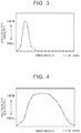
- FIG. 3 is a characteristic diagram showing an exemplary spectroscopic intensity of a light source
- FIG. 4 is a characteristic diagram showing an exemplary spectroscopic sensitivity of a light receiving element
- FIG. 5 is a characteristic diagram showing correspondence between a film thickness and a reflectance
- FIG. 6 shows an exemplary situation in which the reflectance fluctuates when the film thickness fluctuates through evaporation
- FIG. 7 shows an exemplary calculation result of the film thickness at the time when the film thickness fluctuates through evaporation
- FIG. 8 is a general block diagram showing an exemplary film thickness measuring device according to the embodiment of the disclosure.
- FIG. 9 is a flowchart showing an exemplary processing procedure of a controller
- FIG. 10 shows an exemplary situation in which the reflectance of a liquid present between a flat surface and a sphere that is in contact with this flat surface fluctuates
- FIG. 11 shows an exemplary calculation result of the film thickness of the liquid present between the flat surface and the sphere that is in contact with this flat surface.
- a reflectance Rf (f is either s denoting an s polarization component or p denoting a p polarization component) at the time when light is incident upon a light-permeable film of a refraction index n and a film thickness d that is on a substrate of a refraction index nm whose surface does not diffuse light from an incidence medium of a refraction index n 0 at an angle ⁇ 0 is obtained
- a relationship between the film thickness and the reflectance is calculated from a spectroscopic intensity of an illuminator with a narrowed-down wavelength range, which is used as a light source, and a spectroscopic sensitivity of a light receiving element as an actually measured value or a catalog specification determined by a maker, and the film thickness is obtained from the actually measured reflectance.
- FIG. 1 is a schematic view showing the interference of the thin film.
- a thin film a light-permeable film
- refraction indices of an incidence medium the thin film 2 and the substrate 1 with respect to polarization components of the light, namely, s-waves and p-waves can be expressed according to the following equations (1) to (6).
- ⁇ 0 S denotes the refraction index of the incidence medium with respect to the s-waves as the polarization component
- ⁇ 0 P denotes the refraction index of the incidence medium with respect to the p-waves as the polarization component
- ⁇ S denotes the refraction index of the thin film 2 with respect to the s-waves as the polarization component
- ⁇ P denotes the refraction index of the thin film 2 with respect to the p-waves as the polarization component
- ⁇ mS denotes the refraction index of the substrate 1 with respect to the s-waves as the polarization component
- ⁇ mP denotes the refraction index of the substrate 1 with respect to the p-waves as the polarization component.
- ⁇ denotes a refraction angle of light in the thin film 2
- ⁇ m denotes an output angle of light from the substrate 1 .
- ⁇ 0 S n 0 ⁇ cos ⁇ 0 (1)
- ⁇ 0 P n 0/cos ⁇ 0 (2)
- ⁇ S n ⁇ cos ⁇ (3)
- ⁇ P n /cos ⁇ (4)
- ⁇ mS nm ⁇ cos ⁇ m (5)
- ⁇ mP nm /cos ⁇ m (6)
- equations (8) and (9) can be derived.
- Fresnel reflection coefficients on respective interfaces of the s-waves and p-waves as the polarization components of light can be expressed according to the following equations (11) to (14).
- ⁇ 0 S denotes the Fresnel reflection coefficient of the s-waves as the polarization component on a surface of the thin film 2
- ⁇ 1 S denotes the Fresnel reflection coefficient of the s-waves as the polarization component on the interface between the thin film 2 and the substrate 1
- ⁇ 0 P denotes the Fresnel reflection coefficient of the p-waves as the polarization component on the surface of the thin film 2
- ⁇ 1 P denotes the Fresnel reflection coefficient of the p-waves as the polarization component on the interface between the thin film 2 and the substrate 1 .
- ⁇ 0 S ( ⁇ 0 S ⁇ S )/( ⁇ 0 S+ ⁇ S ) (11)
- ⁇ 1 S ( ⁇ S ⁇ mS )/( ⁇ S+ ⁇ mS ) (12)
- ⁇ 0 P ( ⁇ 0 P ⁇ P )/( ⁇ 0 P+ ⁇ P ) (13)
- ⁇ 1 P ( ⁇ P ⁇ mP )/( ⁇ P+ ⁇ mP ) (14)
- FIG. 2 shows a spectroscopic spectrum obtained from the equation (16).
- the axis of abscissa represents a wavelength
- the axis of ordinate represents a reflectance.
- d 1 denotes characteristics in the case where the film thickness of the thin film 2 is equal to 100 nm
- d 2 denotes characteristics in the case where the film thickness of the thin film 2 is equal to 250 nm
- d 3 denotes characteristics in the case where the film thickness of the thin film 2 is equal to 500 nm.
- a relationship between the film thickness of the thin film 2 and the reflectance as shown in FIG. 5 can be obtained from the spectroscopic spectrum shown in FIG.
- a spectroscopic intensity I( ⁇ ) of the light source of the light incident upon the thin film 2 as shown in FIG. 3 a spectroscopic intensity I( ⁇ ) of the light source of the light incident upon the thin film 2 as shown in FIG. 3
- a spectroscopic sensitivity S( ⁇ ) of the light receiving element that photographs the light reflected by the thin film 2 as shown in FIG. 4 .
- the axis of abscissa represents the wavelength
- the axis of ordinate represents a spectroscopic intensity I of the light source.
- the axis of abscissa represents the wavelength
- the axis of ordinate represents a spectroscopic sensitivity S of the light receiving element.
- the axis of abscissa represents the film thickness
- the axis of ordinate represents the reflectance.
- the refraction index n of the thin film 2 is equal to 1.33
- the incidence angle ⁇ 0 of the light incident upon the thin film 2 is equal to 8°.
- characteristics ⁇ 1 indicate the reflectance in the case where the wavelength of the light incident upon the thin film 2 is equal to 450 nm
- characteristics ⁇ 2 indicate the reflectance in the case where the wavelength of the light incident upon the thin film 2 is equal to 530 nm
- characteristics ⁇ 3 indicate the reflectance in the case where the wavelength of the light incident upon the thin film 2 is equal to 650 nm.
- the film thickness decreases with the lapse of time when the thin film 2 is formed of an evaporable material, for example, water or the like. That is, when the reflectance of the thin film 2 in a process till the end of evaporation is measured, the reflectance increases or decreases as the film thickness fluctuates, as shown in FIG. 6 . Then, the reflectance is maximized when evaporation of the thin film 2 ends, namely, when the film thickness of the thin film 2 is equal to zero.
- the axis of abscissa represents an elapsed time
- the axis of ordinate represents the reflectance.
- the film thickness monotonously decreases through evaporation with the lapse of time, and the reflectance oscillates as the film thickness fluctuates. Then, when the film thickness becomes equal to zero at a time point t 1 , the reflectance reaches a peak on a mountain side and thereafter remains equal to this peak value. The film thickness of the thin film 2 becomes equal to zero exactly when the reflectance starts remaining equal to the peak value.
- FIG. 6 shows an actually measured value of a change in the reflectance until the end of evaporation of the thin film 2 .
- tracing back to a time point t 0 from the time point t 1 when the film thickness becomes equal to zero is equivalent to increases in the film thickness from zero, and the reflectance changes according to characteristics similar to those of FIG. 5 in accordance with the process of tracing back from the time point t 1 when the film thickness becomes equal to zero (as the film thickness increases from zero).
- a signal waveform indicating changes in the reflectance when tracing back to the time point t 0 from the time point t 1 in FIG. 6 is similar in shape to a signal waveform indicating changes in the reflectance from the time point when the film thickness becomes equal to zero to a time point when the film thickness becomes equal to dX in FIG. 5 . That is, a position of the time point t 0 on the signal waveform of the reflectance shown in FIG. 6 and a position of the film thickness dX on the signal waveform of the reflectance shown in FIG. 5 substantially coincide with each other.
- the film thickness at a spot that coincides with the position of the time point t 0 on the signal waveform of the reflectance shown in FIG. 6 can be regarded as the film thickness dX at the time point t 0 on the signal waveform of the reflectance shown in FIG. 6 .
- the film thickness at the spot that coincides with the position of the time point t 0 on the signal waveform of the reflectance shown in FIG. 5 in the case where the film thickness at the spot that coincides with the position of the time point t 0 on the signal waveform of the reflectance shown in FIG.
- the reflectance 6 cannot be obtained due to a calculation cycle or the like of the reflectance, it is appropriate, for example, to complement the signal waveform of the reflectance, obtain a signal waveform of the reflectance consisting of an analog signal, and acquire, from this signal waveform, the film thickness at the spot that coincides with the position of the time point t 0 .
- a signal waveform of the reflectance consisting of a digital signal a film thickness at a spot closest to the position of the time point t 0 may be acquired.
- the time point t 0 is located between the fifth peak and the sixth peak (within a time range) in the process of tracing back peaks of the reflectance from the time point t 1 in the sequence of valleys and mountains of the reflectance. If this is collated with a reference spot, that is, the spot where the film thickness is equal to zero in FIG. 5 , the time range specified in FIG. 6 corresponds to a range between the fifth peak and the sixth peak (a film thickness range E 1 in FIG.
- the film thickness is equal to about 490 nm at a spot where the reflectance is equal to rX (e.g., about 0.030), so this film thickness coincides with the film thickness dX at the time point t 0 in FIG. 6 . That is, the film thickness dX of the thin film 2 at the time point t 0 can be estimated from a situation of change in the reflectance until the film thickness of this thin film 2 becomes equal to zero.
- FIG. 7 shows how the film thickness fluctuates in the case where the film thickness is calculated as the reflectance fluctuates as shown in FIG. 6 , according to the aforementioned method.
- the axis of abscissa represents the elapsed time
- the axis of ordinate represents the film thickness. It has been confirmed that the film thickness of the thin film 2 decreases as the thin film 2 evaporates, and that the film thickness of the thin film 2 becomes equal to zero at the time point t 1 when evaporation of the thin film 2 ends.
- FIG. 8 is a schematic block diagram showing an exemplary film thickness measuring device that measures the film thickness through the use of the film thickness measuring method according to the embodiment of the disclosure.
- the film thickness measuring device 10 is equipped with a light source 12 , such as an LED display or the like, that planarly irradiates a surface of a glass 11 as a substrate on which the thin film 2 to be measured is formed with monochromatic light, an image capturing device 13 as a two-dimensional area sensor such as a black-and-white area camera or the like, and a controller 14 .
- the light source 12 and the image capturing device 13 are arranged in such a manner as not to change their relative positions during measurement.
- the film thickness measuring device 10 is equipped with, for example, a blackout curtain 15 for blocking light to prevent the light other than that which is reflected by the light source 12 from being incident upon the image capturing device 13 .
- the thin film 2 may be a film exhibiting light permeability and volatility, such as a water film or the like.
- the glass 11 may not necessarily be applied as the substrate.
- the substrate may be any member having a specular reflecting surface such as a glass, mirror or resin or the like whose surface does not diffuse light, instead of a frosted glass or the like whose surface diffuses light.
- the light source 12 can include, within a field of vision thereof, an entire regular reflection region of a measurement region of the thin film 2 as viewed from the image capturing device 13 , in accordance with the size of the measuring region.
- the wavelength of the light source 12 may be set such that sufficient increasing/decreasing characteristics of the reflectance can be obtained as a reflected light intensity signal shown in FIG. 6 .
- the resolution capability improves and the quality of the acquired increasing/decreasing characteristics improves as the wavelength shortens.
- a purple or blue LED light source or a laser light source can be applied as the light source 12 .
- a maximum intensity is found at a wavelength shorter than about 500 nm where the reflectance greatly changes when the film thickness of the thin film 2 becomes smaller than about 100 nm.
- the image capturing device 13 is installed in a regular reflection direction (a specular reflection direction) of the light source 12 with respect to the surface of the glass 11 .
- the controller 14 is equipped with an input device 14 a , a display device 14 b , and a storage device 14 c .
- the controller 14 performs operation control of the light source 12 and the image capturing device 13 , inputs thereto a captured image obtained by photographing reflected light produced through irradiation of the thin film 2 by the light source 12 through the use of the image capturing device 13 , stores the captured image into the storage device 14 c , and estimates the film thickness of the thin film 2 based on the captured image stored in the storage device 14 c .
- an estimation signal indicating correspondence between the film thickness and the reflectance as shown in FIG. 5 is stored in the storage device 14 c .
- This estimation signal is estimated in advance based on a spectroscopic spectrum obtained as to a model of the thin film 2 to be measured as shown in FIG. 2 , spectroscopic intensity characteristics of the light source 12 as shown in FIG. 3 , and spectroscopic sensitivity characteristics of the light receiving element of the image capturing device 13 as shown in FIG. 4 (function as an estimation signal acquisition unit).
- An operator first commands the start of measurement of the film thickness by, for example, operating the input device 14 a of the controller 14 .
- the controller 14 drivingly controls the light source 12 and the image capturing device 13 (step S 1 ), planarly irradiates a measurement target region of the thin film 2 with monochromatic light through the use of the light source 12 , and photographs the entire regular reflection region of the measurement target region through the use of the image capturing device 13 , for example, on a regular cycle.
- the controller 14 sequentially reads captured image data photographed by the image capturing device 13 , and starts a process of storing the captured image data thus read into the storage device 14 c (step S 2 ). After the image capturing device 13 starts capturing images and the controller 14 starts reading the captured image data, the operator creates the thin film 2 to be measured on the surface of the glass 11 . Then, when the operator commands the end of measurement of the film thickness, for example, as soon as evaporation of the thin film 2 ends, the controller 14 stops driving the light source 12 and the image capturing device 13 (step S 3 ).
- a series of images including those of the surface of the glass 11 with the thin film 2 not formed thereon, the surface of the glass 11 with the thin film 2 formed thereon, the surface of the glass 11 from which the thin film is evaporating, and the surface of the glass 11 from which the thin film 2 has disappeared after the end of evaporation thereof are stored into the storage device 14 c as captured image data.
- the controller 14 detects a reflected light intensity signal indicating how the reflectance changes with the lapse of time from the start of photographing as shown in FIG.
- step S 4 for each pixel, as to the captured image data stored in the storage device 14 c , and specifies a position of presence of the time point t 0 corresponding to the start of photographing on a signal waveform, namely, a time range with respect to the reflectance rX at the time point t 0 and a time point when the film thickness becomes equal to zero or the time point t 1 when the reflectance stops changing in FIG. 6 (function as a time range specifying unit) (step S 4 ).
- the controller 14 obtains the number of peaks corresponding to valleys and mountains on the signal waveform to the time point t 0 with respect to the time point t 1 , and specifies a range between the last peak among the obtained number of peaks and a peak subsequent thereto, as the time range, with the time point t 1 serving as a base point.
- the controller 14 coordinates a characteristic curve indicating correspondence between the film thickness and the reflectance as shown in FIG. 5 , which is stored in the storage device 14 c , with the time range at the time point t 0 as specified in step S 4 , and specifies the film thickness range E 1 where the time point t 0 on the signal waveform of the characteristic curve shown in FIG. 5 is estimated to be present (function as a film thickness range specifying unit) (step S 5 ).
- the controller 14 detects a film thickness corresponding to the reflectance rX within the film thickness range E 1 , and specifies this film thickness as the film thickness dX at the time point t 0 (function as a film thickness setting unit) (step S 6 ).
- the controller 14 causes the display device 14 b to display the film thickness of each pixel (step S 7 ).
- the controller 14 displays the film thickness of the measurement region of the thin film 2 by, for example, changing the displayed color in accordance with the film thickness, and ends the process.
- the controller 14 detects a situation of change in the reflectance of the thin film 2 till the end of evaporation of the thin film 2 , and detects the film thickness based on this situation of change and characteristics detected in advance as to the film thickness and the reflectance. Therefore, the film thickness can be easily detected with a simple configuration.
- the film thickness can be obtained when the reflectance is known. Therefore, a change in the film thickness can be acquired on a high cycle by, for example, detecting the reflectance on a high cycle.
- the film thickness of the entire measurement target region can be obtained at the same time by photographing the entire measurement target region of the film thickness of the thin film 2 . Therefore, the film thickness of the entire measurement target region at the same time point can be detected surface by surface.
- the film thickness can be obtained when the reflectance can be detected. Therefore, the film thickness can be accurately detected even in the case where the film thickness is relatively small, for example, equal to or smaller than 100 nm or the like. Therefore, even a film thickness smaller than 50 nm, which is difficult to obtain through the method of detecting the film thickness through the use of the spectroscopic interference method according to the related art, can be detected. Therefore, a film that has a small film thickness and that evaporates in a short time, such as a water film or the like formed by a windshield wiper is favorably measured.
- Planar irradiation may be carried out through the use of an LED planar irradiation device with a single wavelength or by irradiating an entire screen surface with LED light.
- the film thickness of the measurement region of the thin film 2 is detected surface by surface has been described, but the disclosure is not limited thereto.
- the film thickness of a single pixel on the thin film 2 can also be detected.
- the same controller 14 carries out the process of collecting the situation of change in the reflectance of the thin film 2 to be measured and the process of calculating the film thickness has been described, but the disclosure is not limited thereto.
- the film thickness may be calculated by another processing device, based on the data representing the situation of change in the reflectance of the thin film 2 to be measured as stored in the storage device 14 c.
- the disclosure is not limited thereto.
- the disclosure is also applicable to a case where the substrate 1 has a curved surface.
- a true value of the film thickness may be detected by subjecting the value of the film thickness calculated on the assumption that the substrate 1 has a flat surface to correction calculation. This correction calculation may be carried out, for example, as follows.
- This correction calculation is carried out based on the foregoing equation (10).
- An inclination from the flat surface of the substrate 1 is denoted by ⁇ in the case where the substrate 1 has no flat surface.
- the true value of the film thickness obtained by performing correction calculation is denoted by d′.
- the change in phase ⁇ in the case where the substrate 1 has a flat surface and the change in phase ⁇ in the case where the substrate 1 has a curved surface are equal to each other, so the following equation (17) can be derived from the foregoing equation (10).
- Equation (17) can be expressed as the following equation (18) by being transformed.
- d′ d ⁇ cos ⁇ /cos( ⁇ + ⁇ ) (18)
- the film thickness d can be corrected through the use of the inclination ⁇ of a measurement point, from the equation (18).
- the incidence angle of the light incident from the light source 12 differs depending on the position in a target region of the film thickness. Therefore, for each irradiation position that is irradiated by the light source 12 , the signal waveform of the reflectance shown in FIG. 5 may be calculated through the use of the incidence angle at the position.
- the film thickness of a liquid present between two objects can be measured through the use of the film thickness measuring method according to the embodiment of the disclosure.
- the film thickness is equal to zero at a location where two objects are in contact with each other, for example, in the case where a sphere is in contact with a flat surface.
- the state where the liquid has finished evaporating is equivalent to the state where the film thickness is equal to zero, namely, a contact position at which the two objects are in contact with each other.
- the change in film thickness caused as a result of evaporation of the liquid corresponds to the change in distance between the two objects, namely, the change in size of the air gap between the two objects that are out of contact with each other.
- the thickness of the air gap substantially uniformly increases as the distance from a contact point increases.
- the film thickness measuring method according to the embodiment of the disclosure is applied to this air gap, the thickness of the air gap at each position can be measured.
- the phenomenon of the change in film thickness of the liquid present between the two objects can be explained by the reflectance ( FIG. 10 ) and the film thickness ( FIG. 11 ), which are obtained by replacing the axis of abscissa in FIGS. 6 and 7 mentioned earlier with an axis of abscissa representing, instead of the elapsed time, a spatial position from the position where the two objects are in contact with each other.
- p 1 denotes a position where the two objects are in contact with each other with the film thickness equal to zero
- p 0 denotes a distance from the position p 1 where the film thickness is equal to zero.
Landscapes
- Physics & Mathematics (AREA)
- General Physics & Mathematics (AREA)
- Engineering & Computer Science (AREA)
- Mechanical Engineering (AREA)
- Length Measuring Devices By Optical Means (AREA)
Abstract
Description
η0S=n0×cos θ0 (1)
η0P=n0/cos η0 (2)
ηS=n×cos θ (3)
ηP=n/cos θ (4)
ηmS=nm×cos θm (5)
ηmP=nm/cos θm (6)
n0×sin θ0=n×sin θ=nm×sin θm (7)
cos θ=(1−sin 2θ)1/2={1−(n0/nm)2×sin 2θ}1/2 (8)
cos θm=(1−sin 2θm)1/2={1−(n0/nm)2×sin 2θm}1/2 (9)
δ=(2π/λ)×n×d×cos θ (10)
ρ0S=(η0S−ηS)/(η0S+ηS) (11)
ρ1S=(ηS−ηmS)/(ηS+ηmS) (12)
ρ0P=(η0P−ηP)/(η0P+ηP) (13)
ρ1P=(ηP−ηmP)/(ηP+ηmP) (14)
ρf=(ρ0f+ρ1fe−i2δ)/(1−ρ0f×ρ1fe−i2δ) (15)
Rf=(ρ0f2+ρ1f2+2ρ0fρ1f cos 2δ)/{1+(ρ0fρ1f)2+2ρ0fρ1f cos 2δ} (16)
δ=(2π/λ)×n×d′×cos(θ+Δθ)=(2π/λ)×n×d×cos θ (17)
d′=d×cos θ/cos(θ+Δθ) (18)
Claims (5)
Applications Claiming Priority (2)
| Application Number | Priority Date | Filing Date | Title |
|---|---|---|---|
| JP2017-136898 | 2017-07-13 | ||
| JP2017136898A JP6550101B2 (en) | 2017-07-13 | 2017-07-13 | Film thickness measuring method and film thickness measuring apparatus |
Publications (2)
| Publication Number | Publication Date |
|---|---|
| US20190017807A1 US20190017807A1 (en) | 2019-01-17 |
| US10690480B2 true US10690480B2 (en) | 2020-06-23 |
Family
ID=62916476
Family Applications (1)
| Application Number | Title | Priority Date | Filing Date |
|---|---|---|---|
| US16/030,898 Active 2038-08-29 US10690480B2 (en) | 2017-07-13 | 2018-07-10 | Film thickness measuring method and film thickness measuring device |
Country Status (4)
| Country | Link |
|---|---|
| US (1) | US10690480B2 (en) |
| EP (1) | EP3428572B1 (en) |
| JP (1) | JP6550101B2 (en) |
| CN (1) | CN109253700B (en) |
Families Citing this family (12)
| Publication number | Priority date | Publication date | Assignee | Title |
|---|---|---|---|---|
| US10816464B2 (en) | 2019-01-23 | 2020-10-27 | Applied Materials, Inc. | Imaging reflectometer |
| FI20195098A1 (en) | 2019-02-12 | 2020-08-13 | Photono Oy | System and method for detecting a wave occurring in/on a membrane |
| US11367292B2 (en) * | 2020-02-24 | 2022-06-21 | Ford Global Technologies, Llc | Road marking detection |
| KR102851276B1 (en) * | 2020-03-06 | 2025-08-28 | 삼성디스플레이 주식회사 | Method of measuring a flatness of an object and appratus for performing the same |
| US11150078B1 (en) | 2020-03-26 | 2021-10-19 | Applied Materials, Inc. | High sensitivity image-based reflectometry |
| US11156566B2 (en) * | 2020-03-26 | 2021-10-26 | Applied Materials, Inc. | High sensitivity image-based reflectometry |
| US11417010B2 (en) | 2020-05-19 | 2022-08-16 | Applied Materials, Inc. | Image based metrology of surface deformations |
| CN111964580B (en) * | 2020-07-30 | 2022-02-11 | 广东工业大学 | Device and method for detecting position and angle of film based on optical lever |
| CN114659451B (en) * | 2020-12-22 | 2025-01-28 | 松山湖材料实验室 | Film thickness measurement method and measuring device |
| CN113048895B (en) * | 2021-03-04 | 2022-08-16 | 上海精测半导体技术有限公司 | Apparatus and method for detecting change of reflected light, and film thickness measuring apparatus |
| CN116045821B (en) * | 2022-08-19 | 2026-02-06 | 天津大学 | Method for measuring anisotropic film based on zero-reflection differential signal |
| GB2641537A (en) * | 2024-06-04 | 2025-12-10 | Oxford Instruments Nanotechnology Tools Ltd | Measuring thin film thickness |
Citations (25)
| Publication number | Priority date | Publication date | Assignee | Title |
|---|---|---|---|---|
| US3869211A (en) * | 1972-06-29 | 1975-03-04 | Canon Kk | Instrument for measuring thickness of thin film |
| US4531838A (en) * | 1981-03-26 | 1985-07-30 | Canon Kabushiki Kaisha | Method and device for controlling the film thickness of evaporated film |
| US4998021A (en) | 1988-11-18 | 1991-03-05 | Dainippon Screen Mfg. Co., Ltd. | Method of detecting an end point of surface treatment |
| US5292605A (en) | 1990-05-18 | 1994-03-08 | Xinix, Inc. | Method for control of photoresist develop processes |
| US5427878A (en) | 1991-06-26 | 1995-06-27 | Digital Equipment Corporation | Semiconductor wafer processing with across-wafer critical dimension monitoring using optical endpoint detection |
| US5862199A (en) * | 1995-08-30 | 1999-01-19 | University Of Guelph | Method and apparatus for measuring thickness of paint layers on substrates using backscattering of x-rays |
| JP2000314612A (en) | 1999-04-30 | 2000-11-14 | Kawatetsu Techno Res Corp | Measurement method for film thickness of light transmission film and film thickness measuring device |
| US6252930B1 (en) * | 1994-08-30 | 2001-06-26 | University Of Guelph | Method and apparatus for measuring thickness of coating layers on substrates using backscattering of x-rays and gamma rays |
| JP2002277215A (en) | 2001-03-14 | 2002-09-25 | Omron Corp | Film thickness measuring method and film thickness sensor using the method |
| US6903340B1 (en) | 2001-10-23 | 2005-06-07 | Juan Cesar Scaiano | Thin film analyzer |
| US20050237537A1 (en) | 2004-04-22 | 2005-10-27 | Ilya Leizerson | Determination of thin film topograhpy |
| US20070121124A1 (en) * | 2005-11-29 | 2007-05-31 | Nataliya Nabatova-Gabain | Sample analyzing method, sample analyzing apparatus, manufacturing method of organic EL element, manufacturing equipment, and recording medium |
| US20070248751A1 (en) * | 2001-10-26 | 2007-10-25 | Hermosa Thin Film Co., Ltd. | Dynamic film thickness control system/method and its utilization |
| US7339382B1 (en) * | 2004-11-11 | 2008-03-04 | Systems & Materials Research Corporation | Apparatuses and methods for nondestructive microwave measurement of dry and wet film thickness |
| US20110299098A1 (en) * | 2009-08-31 | 2011-12-08 | Toppan Printing Co., Ltd. | Method and device for measuring coating amount, method and device for determining coating amount, coating device and method for manufacturing coating product |
| US20110299097A1 (en) | 2009-03-27 | 2011-12-08 | Hamamatsu Photonics K.K. | Film thickness measurement device and measurement method |
| WO2012115643A1 (en) | 2011-02-24 | 2012-08-30 | Corning Incorporated | Methods and apparatus for the measurement of film thickness |
| JP2012189406A (en) | 2011-03-10 | 2012-10-04 | Technos Kk | Film thickness measuring method and film thickness measuring apparatus |
| US8388408B2 (en) * | 2008-10-10 | 2013-03-05 | Ebara Corporation | Method of making diagram for use in selection of wavelength of light for polishing endpoint detection, method for selecting wavelength of light for polishing endpoint detection, and polishing endpoint detection method |
| US8581602B2 (en) * | 2009-09-02 | 2013-11-12 | Systems And Materials Research Corporation | Method and apparatus for nondestructive measuring of a coating thickness on a curved surface |
| US20170176331A1 (en) * | 2015-12-18 | 2017-06-22 | Disco Corporation | Protective film detecting method for laser processing |
| US9757027B2 (en) * | 2014-03-06 | 2017-09-12 | Adom, Advanced Optical Technologies Ltd. | System and method for performing tear film structure measurement and evaporation rate measurements |
| US20180038681A1 (en) * | 2015-03-03 | 2018-02-08 | Abb Schweiz Ag | Sensor System And Method For Characterizing A Stack Of Wet Paint Layers |
| US20180119359A1 (en) * | 2012-10-09 | 2018-05-03 | Michael Gorden | Yankee dryer profiler and control |
| US20190183333A1 (en) * | 2014-03-06 | 2019-06-20 | Adom, Advanced Optical Technologies Ltd. | System and method for performing tear film structure measurement |
Family Cites Families (5)
| Publication number | Priority date | Publication date | Assignee | Title |
|---|---|---|---|---|
| CN100582655C (en) * | 2005-07-29 | 2010-01-20 | 大日本网目版制造株式会社 | Asymmetric checking device and asymmetric checking method |
| KR101107507B1 (en) * | 2009-03-23 | 2012-01-31 | 에스엔유 프리시젼 주식회사 | Modeling method of reflectivity distribution curve, thickness measurement method and thickness measurement reflectometer |
| KR101537854B1 (en) * | 2013-09-23 | 2015-07-21 | 에스엔유 프리시젼 주식회사 | Apparatus for measuring thickness and method for measuring thickness for the same |
| EP2899497B1 (en) * | 2014-01-28 | 2019-03-13 | ABB Schweiz AG | Sensor system and method for characterizing a wet paint layer |
| JP6290637B2 (en) * | 2014-01-30 | 2018-03-07 | 浜松ホトニクス株式会社 | Film thickness measuring method and film thickness measuring apparatus |
-
2017
- 2017-07-13 JP JP2017136898A patent/JP6550101B2/en active Active
-
2018
- 2018-07-10 EP EP18182751.0A patent/EP3428572B1/en active Active
- 2018-07-10 CN CN201810751730.3A patent/CN109253700B/en active Active
- 2018-07-10 US US16/030,898 patent/US10690480B2/en active Active
Patent Citations (27)
| Publication number | Priority date | Publication date | Assignee | Title |
|---|---|---|---|---|
| US3869211A (en) * | 1972-06-29 | 1975-03-04 | Canon Kk | Instrument for measuring thickness of thin film |
| US4531838A (en) * | 1981-03-26 | 1985-07-30 | Canon Kabushiki Kaisha | Method and device for controlling the film thickness of evaporated film |
| US4998021A (en) | 1988-11-18 | 1991-03-05 | Dainippon Screen Mfg. Co., Ltd. | Method of detecting an end point of surface treatment |
| US5292605A (en) | 1990-05-18 | 1994-03-08 | Xinix, Inc. | Method for control of photoresist develop processes |
| US5427878A (en) | 1991-06-26 | 1995-06-27 | Digital Equipment Corporation | Semiconductor wafer processing with across-wafer critical dimension monitoring using optical endpoint detection |
| US6252930B1 (en) * | 1994-08-30 | 2001-06-26 | University Of Guelph | Method and apparatus for measuring thickness of coating layers on substrates using backscattering of x-rays and gamma rays |
| US5862199A (en) * | 1995-08-30 | 1999-01-19 | University Of Guelph | Method and apparatus for measuring thickness of paint layers on substrates using backscattering of x-rays |
| JP2000314612A (en) | 1999-04-30 | 2000-11-14 | Kawatetsu Techno Res Corp | Measurement method for film thickness of light transmission film and film thickness measuring device |
| JP2002277215A (en) | 2001-03-14 | 2002-09-25 | Omron Corp | Film thickness measuring method and film thickness sensor using the method |
| US6903340B1 (en) | 2001-10-23 | 2005-06-07 | Juan Cesar Scaiano | Thin film analyzer |
| US20070248751A1 (en) * | 2001-10-26 | 2007-10-25 | Hermosa Thin Film Co., Ltd. | Dynamic film thickness control system/method and its utilization |
| US20050237537A1 (en) | 2004-04-22 | 2005-10-27 | Ilya Leizerson | Determination of thin film topograhpy |
| US7339382B1 (en) * | 2004-11-11 | 2008-03-04 | Systems & Materials Research Corporation | Apparatuses and methods for nondestructive microwave measurement of dry and wet film thickness |
| US20070121124A1 (en) * | 2005-11-29 | 2007-05-31 | Nataliya Nabatova-Gabain | Sample analyzing method, sample analyzing apparatus, manufacturing method of organic EL element, manufacturing equipment, and recording medium |
| US8388408B2 (en) * | 2008-10-10 | 2013-03-05 | Ebara Corporation | Method of making diagram for use in selection of wavelength of light for polishing endpoint detection, method for selecting wavelength of light for polishing endpoint detection, and polishing endpoint detection method |
| US20110299097A1 (en) | 2009-03-27 | 2011-12-08 | Hamamatsu Photonics K.K. | Film thickness measurement device and measurement method |
| CN102341670A (en) | 2009-03-27 | 2012-02-01 | 浜松光子学株式会社 | Film thickness measuring apparatus and measuring method |
| US20110299098A1 (en) * | 2009-08-31 | 2011-12-08 | Toppan Printing Co., Ltd. | Method and device for measuring coating amount, method and device for determining coating amount, coating device and method for manufacturing coating product |
| US8581602B2 (en) * | 2009-09-02 | 2013-11-12 | Systems And Materials Research Corporation | Method and apparatus for nondestructive measuring of a coating thickness on a curved surface |
| WO2012115643A1 (en) | 2011-02-24 | 2012-08-30 | Corning Incorporated | Methods and apparatus for the measurement of film thickness |
| CN103003661A (en) | 2011-02-24 | 2013-03-27 | 康宁股份有限公司 | Methods and apparatus for the measurement of film thickness |
| JP2012189406A (en) | 2011-03-10 | 2012-10-04 | Technos Kk | Film thickness measuring method and film thickness measuring apparatus |
| US20180119359A1 (en) * | 2012-10-09 | 2018-05-03 | Michael Gorden | Yankee dryer profiler and control |
| US9757027B2 (en) * | 2014-03-06 | 2017-09-12 | Adom, Advanced Optical Technologies Ltd. | System and method for performing tear film structure measurement and evaporation rate measurements |
| US20190183333A1 (en) * | 2014-03-06 | 2019-06-20 | Adom, Advanced Optical Technologies Ltd. | System and method for performing tear film structure measurement |
| US20180038681A1 (en) * | 2015-03-03 | 2018-02-08 | Abb Schweiz Ag | Sensor System And Method For Characterizing A Stack Of Wet Paint Layers |
| US20170176331A1 (en) * | 2015-12-18 | 2017-06-22 | Disco Corporation | Protective film detecting method for laser processing |
Non-Patent Citations (1)
| Title |
|---|
| Hu, H., et al., "Evaporation of a Sessile Droplet on a Substrate", Journal of Physical Chemistry, Part B, 2002, vol. 106, No. 6, pp. 1334-1344. |
Also Published As
| Publication number | Publication date |
|---|---|
| EP3428572B1 (en) | 2020-05-20 |
| EP3428572A1 (en) | 2019-01-16 |
| US20190017807A1 (en) | 2019-01-17 |
| CN109253700B (en) | 2020-07-14 |
| JP2019020183A (en) | 2019-02-07 |
| JP6550101B2 (en) | 2019-07-24 |
| CN109253700A (en) | 2019-01-22 |
Similar Documents
| Publication | Publication Date | Title |
|---|---|---|
| US10690480B2 (en) | Film thickness measuring method and film thickness measuring device | |
| US11567004B2 (en) | Optical device for measuring the optical properties of materials | |
| KR100490325B1 (en) | Apparatus for measuring characteristics of thin film by means of two-dimensional detector and method of measuring the same | |
| CN110998257B (en) | Vehicle color measurement method and device | |
| JP2005503547A (en) | Apparatus and method for measuring thickness shape and refractive index distribution of multilayer thin film using principle of two-dimensional reflection photometer | |
| JP2017530341A (en) | Optical evaluation of lenses and lens molds | |
| TW200424497A (en) | Optical film tester | |
| TW201035518A (en) | Method for modeling distribution curve of reflectance and method, reflectometer for measuring thickness using the same | |
| JP2008292296A (en) | Method and apparatus for measuring film thickness of transparent film | |
| US20200381312A1 (en) | Overlay measurement using multiple wavelengths | |
| JP2010048604A (en) | Apparatus and method for measuring film thickness | |
| WO2007145224A1 (en) | End inclination angle measuring method, inspecting method and inspecting apparatus for objects having undulations, method for determining the position of illuminating means, irregularity inspecting apparatus, and illuminating position determining apparatus | |
| JP2004279296A (en) | Film thickness acquisition method | |
| CN109341554A (en) | A device and method for measuring film thickness | |
| CN114199524A (en) | A kind of lens surface shape measuring device and method | |
| US20100295939A1 (en) | Table gauge | |
| JP4192038B2 (en) | Surface shape and / or film thickness measuring method and apparatus | |
| JP5226510B2 (en) | System and method for measuring curvature of optical surfaces | |
| JP2008139062A (en) | Spectrum measuring apparatus, and spectrometry | |
| CN114061467A (en) | Lens thickness measuring device and method | |
| TWI692614B (en) | Film thickness measurement device, substrate inspection device, film thickness measurement method and substrate inspection method | |
| CN113624461B (en) | Film uniformity detection system based on line structured light | |
| CN114199525B (en) | Integrated lens measuring device and measuring method thereof | |
| CN102252629A (en) | Three-dimensional shape measuring device, examining device and adjusting method for three-dimensional shape measurement | |
| JP2019060713A (en) | Refractive index measuring apparatus and refractive index measuring method |
Legal Events
| Date | Code | Title | Description |
|---|---|---|---|
| FEPP | Fee payment procedure |
Free format text: ENTITY STATUS SET TO UNDISCOUNTED (ORIGINAL EVENT CODE: BIG.); ENTITY STATUS OF PATENT OWNER: LARGE ENTITY |
|
| AS | Assignment |
Owner name: TOYOTA JIDOSHA KABUSHIKI KAISHA, JAPAN Free format text: ASSIGNMENT OF ASSIGNORS INTEREST;ASSIGNORS:KONDO, KOJI;OKADA, NAOTO;ARAMAKI, HIROKATSU;AND OTHERS;SIGNING DATES FROM 20180724 TO 20180809;REEL/FRAME:047039/0783 |
|
| STPP | Information on status: patent application and granting procedure in general |
Free format text: DOCKETED NEW CASE - READY FOR EXAMINATION |
|
| STPP | Information on status: patent application and granting procedure in general |
Free format text: NON FINAL ACTION MAILED |
|
| STPP | Information on status: patent application and granting procedure in general |
Free format text: RESPONSE TO NON-FINAL OFFICE ACTION ENTERED AND FORWARDED TO EXAMINER |
|
| STPP | Information on status: patent application and granting procedure in general |
Free format text: NOTICE OF ALLOWANCE MAILED -- APPLICATION RECEIVED IN OFFICE OF PUBLICATIONS |
|
| STPP | Information on status: patent application and granting procedure in general |
Free format text: PUBLICATIONS -- ISSUE FEE PAYMENT VERIFIED |
|
| STCF | Information on status: patent grant |
Free format text: PATENTED CASE |
|
| MAFP | Maintenance fee payment |
Free format text: PAYMENT OF MAINTENANCE FEE, 4TH YEAR, LARGE ENTITY (ORIGINAL EVENT CODE: M1551); ENTITY STATUS OF PATENT OWNER: LARGE ENTITY Year of fee payment: 4 |