US10685862B2 - Controlling the RF amplitude of an edge ring of a capacitively coupled plasma process device - Google Patents
Controlling the RF amplitude of an edge ring of a capacitively coupled plasma process device Download PDFInfo
- Publication number
- US10685862B2 US10685862B2 US15/394,070 US201615394070A US10685862B2 US 10685862 B2 US10685862 B2 US 10685862B2 US 201615394070 A US201615394070 A US 201615394070A US 10685862 B2 US10685862 B2 US 10685862B2
- Authority
- US
- United States
- Prior art keywords
- ring
- ceramic
- electrode
- edge ring
- substrate support
- Prior art date
- Legal status (The legal status is an assumption and is not a legal conclusion. Google has not performed a legal analysis and makes no representation as to the accuracy of the status listed.)
- Active, expires
Links
Images


Classifications
-
- H—ELECTRICITY
- H01—ELECTRIC ELEMENTS
- H01J—ELECTRIC DISCHARGE TUBES OR DISCHARGE LAMPS
- H01J37/00—Discharge tubes with provision for introducing objects or material to be exposed to the discharge, e.g. for the purpose of examination or processing thereof
- H01J37/32—Gas-filled discharge tubes
- H01J37/32431—Constructional details of the reactor
- H01J37/32623—Mechanical discharge control means
-
- H10P72/722—
-
- H—ELECTRICITY
- H01—ELECTRIC ELEMENTS
- H01J—ELECTRIC DISCHARGE TUBES OR DISCHARGE LAMPS
- H01J37/00—Discharge tubes with provision for introducing objects or material to be exposed to the discharge, e.g. for the purpose of examination or processing thereof
- H01J37/32—Gas-filled discharge tubes
- H01J37/32431—Constructional details of the reactor
-
- H—ELECTRICITY
- H01—ELECTRIC ELEMENTS
- H01L—SEMICONDUCTOR DEVICES NOT COVERED BY CLASS H10
- H01L21/00—Processes or apparatus adapted for the manufacture or treatment of semiconductor or solid state devices or of parts thereof
- H01L21/67—Apparatus specially adapted for handling semiconductor or electric solid state devices during manufacture or treatment thereof; Apparatus specially adapted for handling wafers during manufacture or treatment of semiconductor or electric solid state devices or components ; Apparatus not specifically provided for elsewhere
- H01L21/683—Apparatus specially adapted for handling semiconductor or electric solid state devices during manufacture or treatment thereof; Apparatus specially adapted for handling wafers during manufacture or treatment of semiconductor or electric solid state devices or components ; Apparatus not specifically provided for elsewhere for supporting or gripping
- H01L21/6831—Apparatus specially adapted for handling semiconductor or electric solid state devices during manufacture or treatment thereof; Apparatus specially adapted for handling wafers during manufacture or treatment of semiconductor or electric solid state devices or components ; Apparatus not specifically provided for elsewhere for supporting or gripping using electrostatic chucks
- H01L21/6833—Details of electrostatic chucks
-
- H—ELECTRICITY
- H01—ELECTRIC ELEMENTS
- H01J—ELECTRIC DISCHARGE TUBES OR DISCHARGE LAMPS
- H01J37/00—Discharge tubes with provision for introducing objects or material to be exposed to the discharge, e.g. for the purpose of examination or processing thereof
- H01J37/32—Gas-filled discharge tubes
- H01J37/32009—Arrangements for generation of plasma specially adapted for examination or treatment of objects, e.g. plasma sources
- H01J37/32082—Radio frequency generated discharge
- H01J37/32091—Radio frequency generated discharge the radio frequency energy being capacitively coupled to the plasma
-
- H—ELECTRICITY
- H01—ELECTRIC ELEMENTS
- H01J—ELECTRIC DISCHARGE TUBES OR DISCHARGE LAMPS
- H01J37/00—Discharge tubes with provision for introducing objects or material to be exposed to the discharge, e.g. for the purpose of examination or processing thereof
- H01J37/32—Gas-filled discharge tubes
- H01J37/32009—Arrangements for generation of plasma specially adapted for examination or treatment of objects, e.g. plasma sources
- H01J37/32082—Radio frequency generated discharge
- H01J37/321—Radio frequency generated discharge the radio frequency energy being inductively coupled to the plasma
-
- H—ELECTRICITY
- H01—ELECTRIC ELEMENTS
- H01J—ELECTRIC DISCHARGE TUBES OR DISCHARGE LAMPS
- H01J37/00—Discharge tubes with provision for introducing objects or material to be exposed to the discharge, e.g. for the purpose of examination or processing thereof
- H01J37/32—Gas-filled discharge tubes
- H01J37/32009—Arrangements for generation of plasma specially adapted for examination or treatment of objects, e.g. plasma sources
- H01J37/32082—Radio frequency generated discharge
- H01J37/32137—Radio frequency generated discharge controlling of the discharge by modulation of energy
- H01J37/32146—Amplitude modulation, includes pulsing
-
- H—ELECTRICITY
- H01—ELECTRIC ELEMENTS
- H01J—ELECTRIC DISCHARGE TUBES OR DISCHARGE LAMPS
- H01J37/00—Discharge tubes with provision for introducing objects or material to be exposed to the discharge, e.g. for the purpose of examination or processing thereof
- H01J37/32—Gas-filled discharge tubes
- H01J37/32009—Arrangements for generation of plasma specially adapted for examination or treatment of objects, e.g. plasma sources
- H01J37/32082—Radio frequency generated discharge
- H01J37/32174—Circuits specially adapted for controlling the RF discharge
-
- H—ELECTRICITY
- H01—ELECTRIC ELEMENTS
- H01J—ELECTRIC DISCHARGE TUBES OR DISCHARGE LAMPS
- H01J37/00—Discharge tubes with provision for introducing objects or material to be exposed to the discharge, e.g. for the purpose of examination or processing thereof
- H01J37/32—Gas-filled discharge tubes
- H01J37/32431—Constructional details of the reactor
- H01J37/32458—Vessel
- H01J37/32477—Vessel characterised by the means for protecting vessels or internal parts, e.g. coatings
-
- H—ELECTRICITY
- H01—ELECTRIC ELEMENTS
- H01J—ELECTRIC DISCHARGE TUBES OR DISCHARGE LAMPS
- H01J37/00—Discharge tubes with provision for introducing objects or material to be exposed to the discharge, e.g. for the purpose of examination or processing thereof
- H01J37/32—Gas-filled discharge tubes
- H01J37/32431—Constructional details of the reactor
- H01J37/32532—Electrodes
- H01J37/32541—Shape
-
- H—ELECTRICITY
- H01—ELECTRIC ELEMENTS
- H01J—ELECTRIC DISCHARGE TUBES OR DISCHARGE LAMPS
- H01J37/00—Discharge tubes with provision for introducing objects or material to be exposed to the discharge, e.g. for the purpose of examination or processing thereof
- H01J37/32—Gas-filled discharge tubes
- H01J37/32431—Constructional details of the reactor
- H01J37/32532—Electrodes
- H01J37/32568—Relative arrangement or disposition of electrodes; moving means
-
- H—ELECTRICITY
- H01—ELECTRIC ELEMENTS
- H01J—ELECTRIC DISCHARGE TUBES OR DISCHARGE LAMPS
- H01J37/00—Discharge tubes with provision for introducing objects or material to be exposed to the discharge, e.g. for the purpose of examination or processing thereof
- H01J37/32—Gas-filled discharge tubes
- H01J37/32431—Constructional details of the reactor
- H01J37/32532—Electrodes
- H01J37/32577—Electrical connecting means
-
- H—ELECTRICITY
- H01—ELECTRIC ELEMENTS
- H01J—ELECTRIC DISCHARGE TUBES OR DISCHARGE LAMPS
- H01J37/00—Discharge tubes with provision for introducing objects or material to be exposed to the discharge, e.g. for the purpose of examination or processing thereof
- H01J37/32—Gas-filled discharge tubes
- H01J37/32431—Constructional details of the reactor
- H01J37/32532—Electrodes
- H01J37/32605—Removable or replaceable electrodes or electrode systems
-
- H—ELECTRICITY
- H01—ELECTRIC ELEMENTS
- H01J—ELECTRIC DISCHARGE TUBES OR DISCHARGE LAMPS
- H01J37/00—Discharge tubes with provision for introducing objects or material to be exposed to the discharge, e.g. for the purpose of examination or processing thereof
- H01J37/32—Gas-filled discharge tubes
- H01J37/32431—Constructional details of the reactor
- H01J37/32697—Electrostatic control
-
- H—ELECTRICITY
- H01—ELECTRIC ELEMENTS
- H01J—ELECTRIC DISCHARGE TUBES OR DISCHARGE LAMPS
- H01J37/00—Discharge tubes with provision for introducing objects or material to be exposed to the discharge, e.g. for the purpose of examination or processing thereof
- H01J37/32—Gas-filled discharge tubes
- H01J37/32431—Constructional details of the reactor
- H01J37/32715—Workpiece holder
- H01J37/32724—Temperature
-
- H—ELECTRICITY
- H01—ELECTRIC ELEMENTS
- H01J—ELECTRIC DISCHARGE TUBES OR DISCHARGE LAMPS
- H01J37/00—Discharge tubes with provision for introducing objects or material to be exposed to the discharge, e.g. for the purpose of examination or processing thereof
- H01J37/32—Gas-filled discharge tubes
- H01J37/32431—Constructional details of the reactor
- H01J37/32798—Further details of plasma apparatus not provided for in groups H01J37/3244 - H01J37/32788; special provisions for cleaning or maintenance of the apparatus
- H01J37/3288—Maintenance
-
- H—ELECTRICITY
- H01—ELECTRIC ELEMENTS
- H01L—SEMICONDUCTOR DEVICES NOT COVERED BY CLASS H10
- H01L21/00—Processes or apparatus adapted for the manufacture or treatment of semiconductor or solid state devices or of parts thereof
- H01L21/67—Apparatus specially adapted for handling semiconductor or electric solid state devices during manufacture or treatment thereof; Apparatus specially adapted for handling wafers during manufacture or treatment of semiconductor or electric solid state devices or components ; Apparatus not specifically provided for elsewhere
- H01L21/67005—Apparatus not specifically provided for elsewhere
- H01L21/67011—Apparatus for manufacture or treatment
- H01L21/67017—Apparatus for fluid treatment
-
- H—ELECTRICITY
- H01—ELECTRIC ELEMENTS
- H01L—SEMICONDUCTOR DEVICES NOT COVERED BY CLASS H10
- H01L21/00—Processes or apparatus adapted for the manufacture or treatment of semiconductor or solid state devices or of parts thereof
- H01L21/67—Apparatus specially adapted for handling semiconductor or electric solid state devices during manufacture or treatment thereof; Apparatus specially adapted for handling wafers during manufacture or treatment of semiconductor or electric solid state devices or components ; Apparatus not specifically provided for elsewhere
- H01L21/67005—Apparatus not specifically provided for elsewhere
- H01L21/67011—Apparatus for manufacture or treatment
- H01L21/67098—Apparatus for thermal treatment
- H01L21/67103—Apparatus for thermal treatment mainly by conduction
-
- H—ELECTRICITY
- H01—ELECTRIC ELEMENTS
- H01L—SEMICONDUCTOR DEVICES NOT COVERED BY CLASS H10
- H01L21/00—Processes or apparatus adapted for the manufacture or treatment of semiconductor or solid state devices or of parts thereof
- H01L21/67—Apparatus specially adapted for handling semiconductor or electric solid state devices during manufacture or treatment thereof; Apparatus specially adapted for handling wafers during manufacture or treatment of semiconductor or electric solid state devices or components ; Apparatus not specifically provided for elsewhere
- H01L21/67005—Apparatus not specifically provided for elsewhere
- H01L21/67011—Apparatus for manufacture or treatment
- H01L21/67155—Apparatus for manufacturing or treating in a plurality of work-stations
- H01L21/6719—Apparatus for manufacturing or treating in a plurality of work-stations characterized by the construction of the processing chambers, e.g. modular processing chambers
-
- H—ELECTRICITY
- H01—ELECTRIC ELEMENTS
- H01L—SEMICONDUCTOR DEVICES NOT COVERED BY CLASS H10
- H01L21/00—Processes or apparatus adapted for the manufacture or treatment of semiconductor or solid state devices or of parts thereof
- H01L21/67—Apparatus specially adapted for handling semiconductor or electric solid state devices during manufacture or treatment thereof; Apparatus specially adapted for handling wafers during manufacture or treatment of semiconductor or electric solid state devices or components ; Apparatus not specifically provided for elsewhere
- H01L21/683—Apparatus specially adapted for handling semiconductor or electric solid state devices during manufacture or treatment thereof; Apparatus specially adapted for handling wafers during manufacture or treatment of semiconductor or electric solid state devices or components ; Apparatus not specifically provided for elsewhere for supporting or gripping
- H01L21/6831—Apparatus specially adapted for handling semiconductor or electric solid state devices during manufacture or treatment thereof; Apparatus specially adapted for handling wafers during manufacture or treatment of semiconductor or electric solid state devices or components ; Apparatus not specifically provided for elsewhere for supporting or gripping using electrostatic chucks
-
- H—ELECTRICITY
- H01—ELECTRIC ELEMENTS
- H01L—SEMICONDUCTOR DEVICES NOT COVERED BY CLASS H10
- H01L21/00—Processes or apparatus adapted for the manufacture or treatment of semiconductor or solid state devices or of parts thereof
- H01L21/67—Apparatus specially adapted for handling semiconductor or electric solid state devices during manufacture or treatment thereof; Apparatus specially adapted for handling wafers during manufacture or treatment of semiconductor or electric solid state devices or components ; Apparatus not specifically provided for elsewhere
- H01L21/683—Apparatus specially adapted for handling semiconductor or electric solid state devices during manufacture or treatment thereof; Apparatus specially adapted for handling wafers during manufacture or treatment of semiconductor or electric solid state devices or components ; Apparatus not specifically provided for elsewhere for supporting or gripping
- H01L21/687—Apparatus specially adapted for handling semiconductor or electric solid state devices during manufacture or treatment thereof; Apparatus specially adapted for handling wafers during manufacture or treatment of semiconductor or electric solid state devices or components ; Apparatus not specifically provided for elsewhere for supporting or gripping using mechanical means, e.g. chucks, clamps or pinches
- H01L21/68714—Apparatus specially adapted for handling semiconductor or electric solid state devices during manufacture or treatment thereof; Apparatus specially adapted for handling wafers during manufacture or treatment of semiconductor or electric solid state devices or components ; Apparatus not specifically provided for elsewhere for supporting or gripping using mechanical means, e.g. chucks, clamps or pinches the wafers being placed on a susceptor, stage or support
- H01L21/68735—Apparatus specially adapted for handling semiconductor or electric solid state devices during manufacture or treatment thereof; Apparatus specially adapted for handling wafers during manufacture or treatment of semiconductor or electric solid state devices or components ; Apparatus not specifically provided for elsewhere for supporting or gripping using mechanical means, e.g. chucks, clamps or pinches the wafers being placed on a susceptor, stage or support characterised by edge profile or support profile
-
- H—ELECTRICITY
- H01—ELECTRIC ELEMENTS
- H01L—SEMICONDUCTOR DEVICES NOT COVERED BY CLASS H10
- H01L21/00—Processes or apparatus adapted for the manufacture or treatment of semiconductor or solid state devices or of parts thereof
- H01L21/67—Apparatus specially adapted for handling semiconductor or electric solid state devices during manufacture or treatment thereof; Apparatus specially adapted for handling wafers during manufacture or treatment of semiconductor or electric solid state devices or components ; Apparatus not specifically provided for elsewhere
- H01L21/683—Apparatus specially adapted for handling semiconductor or electric solid state devices during manufacture or treatment thereof; Apparatus specially adapted for handling wafers during manufacture or treatment of semiconductor or electric solid state devices or components ; Apparatus not specifically provided for elsewhere for supporting or gripping
- H01L21/687—Apparatus specially adapted for handling semiconductor or electric solid state devices during manufacture or treatment thereof; Apparatus specially adapted for handling wafers during manufacture or treatment of semiconductor or electric solid state devices or components ; Apparatus not specifically provided for elsewhere for supporting or gripping using mechanical means, e.g. chucks, clamps or pinches
- H01L21/68714—Apparatus specially adapted for handling semiconductor or electric solid state devices during manufacture or treatment thereof; Apparatus specially adapted for handling wafers during manufacture or treatment of semiconductor or electric solid state devices or components ; Apparatus not specifically provided for elsewhere for supporting or gripping using mechanical means, e.g. chucks, clamps or pinches the wafers being placed on a susceptor, stage or support
- H01L21/68785—Apparatus specially adapted for handling semiconductor or electric solid state devices during manufacture or treatment thereof; Apparatus specially adapted for handling wafers during manufacture or treatment of semiconductor or electric solid state devices or components ; Apparatus not specifically provided for elsewhere for supporting or gripping using mechanical means, e.g. chucks, clamps or pinches the wafers being placed on a susceptor, stage or support characterised by the mechanical construction of the susceptor, stage or support
-
- H10P72/0402—
-
- H10P72/0432—
-
- H10P72/0462—
-
- H10P72/72—
-
- H10P72/7611—
-
- H10P72/7624—
-
- H—ELECTRICITY
- H01—ELECTRIC ELEMENTS
- H01J—ELECTRIC DISCHARGE TUBES OR DISCHARGE LAMPS
- H01J2237/00—Discharge tubes exposing object to beam, e.g. for analysis treatment, etching, imaging
- H01J2237/32—Processing objects by plasma generation
- H01J2237/33—Processing objects by plasma generation characterised by the type of processing
- H01J2237/332—Coating
-
- H—ELECTRICITY
- H01—ELECTRIC ELEMENTS
- H01J—ELECTRIC DISCHARGE TUBES OR DISCHARGE LAMPS
- H01J2237/00—Discharge tubes exposing object to beam, e.g. for analysis treatment, etching, imaging
- H01J2237/32—Processing objects by plasma generation
- H01J2237/33—Processing objects by plasma generation characterised by the type of processing
- H01J2237/334—Etching
Definitions
- aspects of the present disclosure generally relate to apparatuses and methods for controlling the RF amplitude of an edge ring in a processing chamber.
- An edge ring is a circular component which surrounds a perimeter of a substrate, such as a semiconductor wafer, during processing in process chamber. Due to exposure of the edge ring to plasma within the process chamber, the edge ring may erode and require replacement or other preventative maintenance after a predetermined interval. When the edge ring is eroded too much, the plasma sheath at the edge of the substrate drops lower and changes the plasma processing characteristics at the edge of the substrate. The change in plasma processing characteristics causes undesirable processing effects at the edge of the substrate, thus reducing the usable real estate near the edge of the substrate.
- a substrate support comprises an electrostatic chuck having one or more chucking electrodes embedded therein for chucking a substrate to the electrostatic chuck; a ceramic layer disposed over the electrostatic chuck; a ceramic ring positioned around the ceramic layer; an electrode embedded in the ceramic ring; and a variable capacitor coupled to the electrode through one or more transmission lines.
- a process chamber comprises a chamber body; a lid disposed on the chamber body; an inductively coupled plasma apparatus positioned above the lid; and a substrate support positioned within the chamber body, the substrate support comprising: an electrostatic chuck having one or more chucking electrodes embedded therein for chucking a substrate to the electrostatic chuck; a ceramic layer disposed over the electrostatic chuck; a ceramic ring positioned around the ceramic layer; an electrode embedded in the ceramic ring, the electrode coupled to a variable capacitor through one or more transmission lines.
- a method of processing substrate comprises processing a predetermined amount of substrates using a plasma sheath, resulting in erosion of an edge ring; increasing RF voltage at the edge ring after the erosion to reposition the plasma sheath; and processing additional substrates after the increasing the RF voltage to alter the erosion of the edge ring.
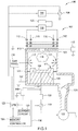
- FIG. 1 is a schematic sectional view of a process chamber, according to one aspect of the disclosure.
- FIGS. 2A and 2B illustrate enlarged schematic views of the substrate support shown in FIG. 1 .
- FIGS. 3A-3C are schematic views of a plasma sheath relative to the perimeter of a substrate, according to aspects of the disclosure.
- FIGS. 4A and 4B illustrate schematic circuit diagrams, according to one aspect of the disclosure.
- FIG. 5 is a flow diagram illustrating a method of processing substrates, according to one aspect of the disclosure.
- the present disclosure generally relates to apparatuses and methods that control RF amplitude of an edge ring.
- the apparatuses and methods include an electrode that is coupled to ground through a variable capacitor.
- the electrode may be ring-shaped and embedded in a substrate support including an electrostatic chuck.
- the electrode may be positioned beneath the perimeter of a substrate and/or the edge ring.
- the capacitance of the variable capacitor is adjusted in order to affect the RF amplitude near the edge of the substrate. Adjustment of the RF amplitude via the electrode and variable capacitor results in adjustment of the plasma sheath near the substrate perimeter.
- FIG. 1 is a schematic sectional view of a process chamber 100 , according to one aspect of the disclosure.
- the process chamber 100 includes a chamber body 101 and a lid 103 disposed thereon that together define an inner volume.
- the chamber body 101 is typically coupled to an electrical ground 107 .
- a substrate support 111 is disposed within the inner volume to support a substrate 109 thereon.
- the process chamber 100 also includes an inductively coupled plasma apparatus 102 for generating a plasma region 118 within the process chamber 100 , and a controller 155 adapted to control aspects of the process chamber 100 .
- the substrate support 111 includes one or more electrodes 134 coupled to a bias source 119 through a matching network 120 , and a circular electrode 139 coupled to ground through a variable capacitor 140 .
- the inductively coupled plasma apparatus 102 is typically disposed above the lid 103 and is configured to inductively couple RF power into the process chamber 100 .
- the inductively coupled plasma apparatus 102 includes first and second coils 110 , 112 , disposed above the lid 103 . The relative position, ratio of diameters of each coil, 110 , 112 and/or the number of turns in each coil 110 , 112 can each be adjusted to control, for example, the profile or density of the plasma region 118 .
- Each of the first and second coils 110 , 112 is coupled through a matching network 114 via the RF feed structure 106 , to an RF power supply 108 .
- the RF power supply 108 may be capable, in one example, of producing up to about 4000 Watts at a tunable frequency in a range from 50 kHz to 13.56 MHz. However, other frequencies and powers may be provided as desired for particular applications.
- a power divider 105 such as a dividing capacitor, may be provided between the RF feed structure 106 and the RF power supply 108 to control the relative quantity of RF power provided to the respective first and second coils 110 , 112 .
- the power divider 105 may be incorporated into the matching network 114 .
- a heater element 113 may be disposed atop the lid 103 to facilitate heating the interior of the process chamber 100 .
- the heater element 113 may be disposed between the lid 103 and the first and second coils 110 , 112 .
- the heater element 113 may include a resistive heating element and may be coupled to a power supply 115 , such as an AC power supply, configured to provide sufficient energy to control the temperature of the heater element 113 within a desired range.
- the substrate 109 (such as a semiconductor wafer or other substrate suitable for plasma processing) may be placed on the substrate support 111 and process gases may be supplied from a gas panel 116 through entry ports 117 .
- the process gases may be ignited into a plasma region 118 in the process chamber 100 by applying power from the RF power supply 108 to the first and second coils 110 , 112 .
- power from a bias source 119 such as an RF or shaped pulse source, may also be provided through a matching network 120 to electrodes 134 within the substrate support 111 .
- the pressure within the interior of the process chamber 100 may be controlled using a valve 121 and a vacuum pump 122 .
- the temperature of the chamber body 101 may be controlled using fluid-containing conduits (not shown) that run through the chamber body 101 .
- the process chamber 100 includes a controller 155 to control aspects of the process chamber 100 during processing.
- the controller 155 comprises a central processing unit (CPU) 123 , a memory 124 , and support circuits 125 for the CPU 123 .
- the controller 155 facilitates control of the components of the process chamber 100 .
- the controller 155 may be one of any form of general-purpose computer that can be used in an industrial setting for controlling various chambers and sub-processors.
- the memory 124 stores software (source or object code) that may be executed or invoked to control the operation of the process chamber 100 in manners described herein.
- FIGS. 2A and 2B illustrate enlarged schematic views of the substrate support 111 shown in FIG. 1 .
- the substrate support 111 includes a ground plate 226 surrounding an insulating layer 227 , a facilities plate 228 , and an electrostatic chuck 229 assembled in a vertical stack.
- a quartz pipe ring 230 circumscribes the facilities plate 228 and the electrostatic chuck 229 to insulate the RF-hot electrostatic chuck 229 from the ground plate 226 .
- a plasma shield 231 is disposed on an upper surface of the quartz pipe ring 230 to facilitate plasma containment in the process chamber 100 (shown in FIG. 1 ).
- a quartz ring 232 is positioned on an upper surface of the plasma shield 231 and includes a lower recess for engaging the quartz pipe ring 230 .
- the facilities plate 228 is positioned between a lower portion of the ground plate 226 and the electrostatic chuck 229 .
- the facilities plate 228 includes a one or more channels 233 (four are shown) through which a fluid is provided to facilitate temperature control of the substrate support 111 .
- the electrostatic chuck 229 includes a plurality of electrodes 134 (four are shown) embedded in an insulating material 236 .
- the electrodes 134 are coupled to the bias source 119 (shown in FIG. 1 ) to facilitate chucking of a substrate 109 to an upper surface of the electrostatic chuck 229 .
- the electrodes 134 are cathodes coupled through a matching network 120 to the bias source 119 .
- the bias source 119 may illustratively be a source of up to about 1000 W (but not limited to about 1000 W) of RF energy at a frequency of, for example, approximately 13.56 MHz, although other frequencies and powers may be provided as desired for particular applications.
- the bias source 119 may be capable of producing either or both of continuous or pulsed power.
- the bias source 119 may be a DC or pulsed DC source.
- the bias source 119 may be capable of providing multiple frequencies, such as 13.56 MHz and 2 MHz.
- a heater 235 is disposed on an upper surface of the electrostatic chuck 229 to facilitate temperature control of the substrate 109 .
- the heater 235 may be, for example, a resistive heater having a plurality of resistive heating elements embedded therein.
- a ceramic layer 237 such as silicon carbide or alumina, is disposed over the upper surface of the heater 235 and provides a protective interface between the heater 235 and the substrate 109 .
- a ceramic ring 238 surrounds and abuts the radially-outward edges of the ceramic layer 237 .
- the ceramic ring 238 may be made of, for example, silicon dioxide or silicon nitride, and may have a thickness within a range of about 1 millimeter to about 2 millimeters.
- a circular electrode 139 is embedded in the ceramic ring 238 .
- the circular electrode 139 may be positioned about 0.5 millimeters to about 1 millimeter from the upper surface of the ceramic ring 238 , such as about 0.75 millimeters.
- the circular electrode 139 may have a width of about 3 millimeters to about 20 millimeters, such as about 6 millimeters.
- the circular electrode 139 is positioned radially outward of the perimeter of the substrate 109 and beneath an edge ring 242 .
- the circular electrode 139 may have an inner diameter greater than 200 millimeters, or greater than 300 millimeters, or greater than 400 millimeters.
- the circular electrode 139 is electrically coupled to ground through a variable capacitor 140 .
- the circular electrode 139 may be coupled to the variable capacitor 140 through multiple transmission lines 141 (one is shown).
- the circular electrode 139 may be coupled to the variable capacitor 140 through three transmission lines 141 spaced about the circular electrode 139 at even intervals (i.e., 120 degrees).
- the utilization of multiple transmission lines 141 may reduce the occurrence of RF or temperature non-uniformities by making any asymmetries of the transmission lines higher order and lower amplitude.
- the edge ring 242 is positioned over the ceramic ring 238 and in contact with the ceramic ring 238 and the ceramic layer 237 .
- the edge ring 242 may be formed from silicon carbide, graphite coated with silicon carbide, or low resistivity doped silicon.
- An upper surface of the edge ring 242 contacts a lower surface of an overhanging ledge of the quartz ring 232 .
- the edge ring 242 circumscribes the substrate 109 and reduces undesired etching or deposition of material at the radially-outward edges of the substrate 109 .
- the substrate 109 is spaced radially from the edge ring 242 to facilitate sealing of the substrate 109 to the electrostatic chuck 229 .
- a plasma sheath 245 may form over the surface of the substrate 109 .
- processing conditions may erode the upper portion of the edge ring 242 , causing undesired processing of the edge of the substrate 109 , such as rollover.
- the undesired processing reduces device yield and affects substrate-to-substrate uniformity.
- conventional approaches frequently replaced the edge ring 242 .
- frequent replacement of the edge ring 242 is expensive from a consumable material point of view, and additionally, requires significant down time.
- aspects described herein utilize a circular electrode 139 coupled to ground through a variable capacitor 140 to adjust the RF amplitude, and thus the plasma sheath, near the edge ring 242 .
- RF power initially delivered to the electrostatic chuck 229 has a high RF coupling with the edge ring 242 .
- the RF amplitude on the edge ring 242 could be higher than the RF amplitude on the substrate 109 .
- Adjustment of the capacitance of the variable capacitor 140 is increased enough that the RF voltage at the edge ring 242 is comparable to the substrate 109 .
- the RF capacitance can be decreased to increase the RF amplitude and therefore the sheath thickness to keep the top of the sheath in approximately the same location.
- the adjustment of the RF amplitude thereby facilitates continued utilization of the eroded edge ring while mitigating undesired processing effects on the substrate 109 .
- a gap 253 may be provided between an upper surface of the ceramic ring 238 and a lower surface of the edge ring 242 .
- the gap 253 may be utilized to decrease coupling between the circular electrode 139 and the plasma sheath 245 .
- the thickness of the gap 253 may be selected to provide a desired amount of decoupling.
- the circular electrode 139 may have another shape, or may include a plurality of distinct electrodes which may be arranged into a desired shape or configuration.
- the length of a transmission line 141 may have a length that is lambda (wavelength) divided by 2 (e.g., ⁇ /2) to facilitate matched impedance, in at least one frequency.
- the width of the electrode 139 may be selected to increase or decrease electrical coupling with the edge ring 242 , as desired.
- an optional gap 253 may be omitted.
- a conductive thermal gasket for example, a silicone-based thermal gasket, may occupy the gap 253 .
- the variable capacitor 140 may be coupled to the RF power supply 108 rather than to ground. In such an aspect, the variable capacitor 140 would facilitate adjustment of capacitive coupling, rather than a parasitic effect as described above.
- FIGS. 3A-3C are schematic views of a plasma sheath 245 relative to the perimeter of a substrate 109 , according to aspects of the disclosure.
- FIG. 3 A illustrates a plasma sheath 245 relative to an edge ring 242 and a substrate 109 prior to erosion of the edge ring 242 .
- the plasma sheath 245 is a layer in a plasma which has a greater density of positive ions, and hence an overall excess positive charge, that balances an opposite negative charge on the surface of a material with which it is in contact.
- the upper surface of the edge ring 242 and the substrate 109 are generally coplanar prior to erosion of the edge ring 242 .
- the plasma sheath 245 Prior to erosion of the edge ring 242 , the plasma sheath 245 is parallel with and equally spaced from the upper surfaces of the edge ring 242 and the substrate 109 .
- the profile of the plasma sheath 245 illustrated in FIG. 3A results in uniform processing of the substrate 109 , particular near the radially-outward edge thereof.
- FIG. 3B illustrates an eroded edge ring 242 .
- the upper surface of the edge ring 242 may be eroded away, thereby reducing the thickness of the edge ring 242 .
- the eroded edge ring 242 no longer shares a coplanar upper surface with a substrate 109 . Due to the interaction between edge ring 242 and charged particles in a plasma, the profile of the plasma sheath 245 is changed in the presence of the eroded edge ring 242 . As illustrated in FIG.
- the plasma sheath 245 drops at the interface of the substrate 109 and the edge ring 242 to maintain equidistant spacing from the surface of the edge ring 242 as compared to the substrate 109 .
- the profile of the plasma sheath 245 may result in “rounding” or other undesired processing of the radially-outward edge of the substrate 109 .
- the rounding of the substrate edge decreases the usable real estate of the substrate 109 , thus decreasing device yield per substrate. This undesired rounding may commonly be referred to as a “rollover effect”.
- the eroded edge ring 242 would be replaced, thus causing processing down time while increasing the cost of consumable parts.
- aspects of the present disclosure utilize a circular electrode 139 to adjust the RF amplitude, and the thus the location of the plasma sheath 245 , above the eroded edge ring 242 .
- the variable capacitor 140 shown in FIG. 2A
- the capacitance to ground acts like part of a capacitive voltage divider with fixed capacitance coupling power from the electrostatic chuck 229 to the edge ring 242 , and a variable capacitance to ground.
- the variable capacitor 140 may be adjusted to short out more or less of the RF power to the edge ring 242 , thereby changing the height of the plasma sheath 245 above the edge ring 242 .
- the variable capacitor 140 and the circular electrode 139 facilitate compensation of the eroded edge ring 242 .
- FIG. 3C illustrates an adjusted plasma sheath 245 adjacent to an eroded edge ring 242 .
- the adjusted plasma sheath 245 does not cause a “rollover effect” on the substrate 109 , thus preventing damage to the substrate 109 and maximizing the usable real estate of the substrate 109 .
- the eroded edge ring 242 may continue to be utilized in an eroded state, the time between preventative maintenances is extended, thereby decreasing processing downtime. Additionally, the eroded edge rings 237 require less frequent replacement, thereby decreasing expenses for consumable parts.
- FIGS. 4A and 4B illustrate schematic circuit diagrams, according to one aspect of the disclosure.
- FIGS. 4A and 4B illustrate an element model 450 within the substrate support 111 .
- FIG. 4A illustrates the element model 450 overlaid on a partial view of the substrate support 111 .
- the term element model is used to describe the functional relationships amongst components of a system, for example, when using a conductive silicon carbide layer having a resistivity less than 10 ohm-centimeter ( ⁇ -cm).
- power is applied from V 0 , e.g., power at the electrostatic chuck 229 from the bias source 119 .
- a capacitance C 1 is present between the baseplate 229 and the edge ring 242 through the heater 235 and the ceramic ring 238 .
- a capacitance C 4 is present between the baseplate 229 and the electrode 139 through the interface of the heater 235 and the ceramic ring 238 .
- a capacitance C 2 is present between the edge ring 242 and a plasma 118 . The capacitance C 2 is coupled to ground through the plasma 118 .
- a capacitance C 3 is present between the edge ring 242 and the electrode 139 through the ceramic 238 .
- a variable capacitor 140 is coupled to ground as well as to the electrode 139 through one or more transmission lines 141 .
- the variable capacitor 140 may be adjusted to control the RF voltage applied to the electrode 139 , as described above.
- the element model 450 is only one example of a circuit, and other circuits are also contemplated.
- FIG. 5 is a flow diagram illustrating a method 560 of processing substrates, according to one aspect of the disclosure.
- the method 560 begins in operation 562 .
- a predetermined number of substrates are processed using a new or refurbished edge ring.
- the new or refurbished edge ring positions the plasma sheath in a known position, such as parallel to the upper surface of the edge ring and a substrate being processed.
- the edge ring erodes, and changes the position of the plasma sheath during processing.
- method 560 proceeds to operation 564 , and the adjustable capacitor is tuned to correct for the deviation in the plasma sheath due to the erosion of the edge ring.
- operation 566 additional substrates are processed while the plasma sheath is maintained in the corrected position by the adjustable capacitor and the electrode. Operations 564 and 566 may then be repeated until the edge ring is unusable or the tunable capacitor is unable to provide sufficient adjustment.
- FIG. 5 describes one aspect of a method 560 , other aspects are also contemplated.
- the edge ring thickness or position of the plasma sheath may be monitored to indicate when operation 564 is to occur.
- Benefits of the disclosure include the ability to adjust plasma sheaths in lieu of replacing chamber components, thereby improving device yield while mitigating downtime and reducing expenditures on consumables. Additionally, aspects described herein allow for the plasma sheath to be adjusted independent of a matching network, thereby greatly simplifying the adjustment of the plasma sheath and the hardware required to do so.
- an electrode is formed in a ceramic layer disposed on or built into an electrostatic chuck.
- the electrode is coupled at one or more locations to high impedance transmission lines.
- the transmission lines are coupled to ground through a variable capacitor.
- the electrode functions as a center of a capacitive voltage divider, between the fixed capacitance of the electrostatic chuck and the electrode, and the variable capacitance to ground.
- the capacitance through the variable capacitor may be decreased as an edge ring is eroded, thus increasing the RF amplitude at the edge ring, at a desirable rate to compensate for the edge ring erosion.
- the increased RF voltage at the edge ring adjusts the location of the plasma sheath to correct for the erosion of the edge ring.
- the RF voltage at the edge ring may be adjusted to be greater than or less than the RF voltage of the substrate, as desired.
Landscapes
- Engineering & Computer Science (AREA)
- Physics & Mathematics (AREA)
- Plasma & Fusion (AREA)
- Analytical Chemistry (AREA)
- Chemical & Material Sciences (AREA)
- Drying Of Semiconductors (AREA)
- General Physics & Mathematics (AREA)
- Power Engineering (AREA)
- Microelectronics & Electronic Packaging (AREA)
- Computer Hardware Design (AREA)
- Manufacturing & Machinery (AREA)
- Condensed Matter Physics & Semiconductors (AREA)
- Container, Conveyance, Adherence, Positioning, Of Wafer (AREA)
- Plasma Technology (AREA)
- Chemical Vapour Deposition (AREA)
Abstract
Description
Claims (20)
Priority Applications (1)
| Application Number | Priority Date | Filing Date | Title |
|---|---|---|---|
| US15/394,070 US10685862B2 (en) | 2016-01-22 | 2016-12-29 | Controlling the RF amplitude of an edge ring of a capacitively coupled plasma process device |
Applications Claiming Priority (3)
| Application Number | Priority Date | Filing Date | Title |
|---|---|---|---|
| US201662286028P | 2016-01-22 | 2016-01-22 | |
| US201662301316P | 2016-02-29 | 2016-02-29 | |
| US15/394,070 US10685862B2 (en) | 2016-01-22 | 2016-12-29 | Controlling the RF amplitude of an edge ring of a capacitively coupled plasma process device |
Publications (2)
| Publication Number | Publication Date |
|---|---|
| US20170213753A1 US20170213753A1 (en) | 2017-07-27 |
| US10685862B2 true US10685862B2 (en) | 2020-06-16 |
Family
ID=58416132
Family Applications (1)
| Application Number | Title | Priority Date | Filing Date |
|---|---|---|---|
| US15/394,070 Active 2038-09-20 US10685862B2 (en) | 2016-01-22 | 2016-12-29 | Controlling the RF amplitude of an edge ring of a capacitively coupled plasma process device |
Country Status (5)
| Country | Link |
|---|---|
| US (1) | US10685862B2 (en) |
| JP (2) | JP6953133B2 (en) |
| KR (1) | KR102721101B1 (en) |
| CN (2) | CN106997842B (en) |
| TW (2) | TWI713078B (en) |
Cited By (12)
| Publication number | Priority date | Publication date | Assignee | Title |
|---|---|---|---|---|
| US11373895B2 (en) * | 2019-07-01 | 2022-06-28 | Tokyo Electron Limited | Etching method and plasma processing apparatus |
| US11446788B2 (en) | 2014-10-17 | 2022-09-20 | Applied Materials, Inc. | Precursor formulations for polishing pads produced by an additive manufacturing process |
| US11471999B2 (en) | 2017-07-26 | 2022-10-18 | Applied Materials, Inc. | Integrated abrasive polishing pads and manufacturing methods |
| US20220399193A1 (en) * | 2021-06-09 | 2022-12-15 | Applied Materials, Inc. | Plasma uniformity control in pulsed dc plasma chamber |
| US11685014B2 (en) | 2018-09-04 | 2023-06-27 | Applied Materials, Inc. | Formulations for advanced polishing pads |
| US11724362B2 (en) | 2014-10-17 | 2023-08-15 | Applied Materials, Inc. | Polishing pads produced by an additive manufacturing process |
| US11745302B2 (en) | 2014-10-17 | 2023-09-05 | Applied Materials, Inc. | Methods and precursor formulations for forming advanced polishing pads by use of an additive manufacturing process |
| US11772229B2 (en) | 2016-01-19 | 2023-10-03 | Applied Materials, Inc. | Method and apparatus for forming porous advanced polishing pads using an additive manufacturing process |
| US11929239B2 (en) | 2021-01-08 | 2024-03-12 | Samsung Electronics Co., Ltd. | Plasma processing apparatus and semiconductor device manufacturing method using the same |
| US11958162B2 (en) | 2014-10-17 | 2024-04-16 | Applied Materials, Inc. | CMP pad construction with composite material properties using additive manufacturing processes |
| US11986922B2 (en) | 2015-11-06 | 2024-05-21 | Applied Materials, Inc. | Techniques for combining CMP process tracking data with 3D printed CMP consumables |
| US12023853B2 (en) | 2014-10-17 | 2024-07-02 | Applied Materials, Inc. | Polishing articles and integrated system and methods for manufacturing chemical mechanical polishing articles |
Families Citing this family (28)
| Publication number | Priority date | Publication date | Assignee | Title |
|---|---|---|---|---|
| KR20170039781A (en) * | 2015-10-01 | 2017-04-12 | 삼성디스플레이 주식회사 | Electrostatic chuck and substrate processing apparatus including the same |
| US10685862B2 (en) * | 2016-01-22 | 2020-06-16 | Applied Materials, Inc. | Controlling the RF amplitude of an edge ring of a capacitively coupled plasma process device |
| US9852889B1 (en) * | 2016-06-22 | 2017-12-26 | Lam Research Corporation | Systems and methods for controlling directionality of ions in an edge region by using an electrode within a coupling ring |
| US10665433B2 (en) * | 2016-09-19 | 2020-05-26 | Varian Semiconductor Equipment Associates, Inc. | Extreme edge uniformity control |
| US10763081B2 (en) | 2017-07-10 | 2020-09-01 | Applied Materials, Inc. | Apparatus and methods for manipulating radio frequency power at an edge ring in plasma process device |
| JP6974088B2 (en) * | 2017-09-15 | 2021-12-01 | 東京エレクトロン株式会社 | Plasma processing equipment and plasma processing method |
| CN109961997B (en) * | 2017-12-22 | 2021-11-16 | 中微半导体设备(上海)股份有限公司 | Plasma processing apparatus and DC bias voltage control method thereof |
| US11387134B2 (en) * | 2018-01-19 | 2022-07-12 | Applied Materials, Inc. | Process kit for a substrate support |
| KR102742830B1 (en) * | 2018-02-28 | 2024-12-12 | 어플라이드 머티어리얼스, 인코포레이티드 | Electrostatic chuck with multiple radio frequency meshes to control plasma uniformity |
| CN110323117B (en) | 2018-03-28 | 2024-06-21 | 三星电子株式会社 | Plasma treatment equipment |
| JP7096079B2 (en) | 2018-06-15 | 2022-07-05 | キオクシア株式会社 | Regeneration device for plasma processing equipment |
| US10867829B2 (en) * | 2018-07-17 | 2020-12-15 | Applied Materials, Inc. | Ceramic hybrid insulator plate |
| KR102111504B1 (en) * | 2018-10-15 | 2020-05-18 | 세메스 주식회사 | Substrate processing apparatus and method |
| KR102595900B1 (en) * | 2018-11-13 | 2023-10-30 | 삼성전자주식회사 | Plasma processing apparatus |
| US10903050B2 (en) * | 2018-12-10 | 2021-01-26 | Lam Research Corporation | Endpoint sensor based control including adjustment of an edge ring parameter for each substrate processed to maintain etch rate uniformity |
| US11955314B2 (en) * | 2019-01-09 | 2024-04-09 | Tokyo Electron Limited | Plasma processing apparatus |
| US10784089B2 (en) | 2019-02-01 | 2020-09-22 | Applied Materials, Inc. | Temperature and bias control of edge ring |
| US12009236B2 (en) * | 2019-04-22 | 2024-06-11 | Applied Materials, Inc. | Sensors and system for in-situ edge ring erosion monitor |
| US11894255B2 (en) * | 2019-07-30 | 2024-02-06 | Applied Materials, Inc. | Sheath and temperature control of process kit |
| WO2021025849A1 (en) * | 2019-08-05 | 2021-02-11 | Applied Materials, Inc. | Coating for chamber particle reduction |
| US20210175103A1 (en) * | 2019-12-06 | 2021-06-10 | Applied Materials, Inc. | In situ failure detection in semiconductor processing chambers |
| US11887820B2 (en) * | 2020-01-10 | 2024-01-30 | COMET Technologies USA, Inc. | Sector shunts for plasma-based wafer processing systems |
| US12542257B2 (en) | 2020-03-04 | 2026-02-03 | Lam Research Corporation | Minimizing reflected power in a tunable edge sheath system |
| JP2021150380A (en) | 2020-03-17 | 2021-09-27 | キオクシア株式会社 | Film treatment method and manufacturing method of semiconductor device |
| JP7450427B2 (en) | 2020-03-25 | 2024-03-15 | 東京エレクトロン株式会社 | Substrate support and plasma processing equipment |
| US11276601B2 (en) * | 2020-04-10 | 2022-03-15 | Applied Materials, Inc. | Apparatus and methods for manipulating power at an edge ring in a plasma processing device |
| JP7740979B2 (en) | 2021-12-13 | 2025-09-17 | 東京エレクトロン株式会社 | Plasma processing apparatus and potential control method |
| JP7741347B1 (en) | 2023-11-17 | 2025-09-17 | 東京エレクトロン株式会社 | Plasma processing equipment |
Citations (43)
| Publication number | Priority date | Publication date | Assignee | Title |
|---|---|---|---|---|
| US5748434A (en) * | 1996-06-14 | 1998-05-05 | Applied Materials, Inc. | Shield for an electrostatic chuck |
| US6039836A (en) | 1997-12-19 | 2000-03-21 | Lam Research Corporation | Focus rings |
| US6232236B1 (en) | 1999-08-03 | 2001-05-15 | Applied Materials, Inc. | Apparatus and method for controlling plasma uniformity in a semiconductor wafer processing system |
| US20010019881A1 (en) * | 2000-03-01 | 2001-09-06 | Yutaka Ohmoto | Plasma processing apparatus and method |
| US20050056622A1 (en) * | 2002-09-18 | 2005-03-17 | Lam Research Corporation | Method and apparatus for the compensation of edge ring wear in a plasma processing chamber |
| CN1851896A (en) | 2005-12-05 | 2006-10-25 | 北京北方微电子基地设备工艺研究中心有限责任公司 | Electrostatic chuck |
| US20090071938A1 (en) * | 2007-06-28 | 2009-03-19 | Rajinder Dhindsa | Methods and apparatus for substrate processing |
| US20090223810A1 (en) | 2007-06-28 | 2009-09-10 | Rajinder Dhindsa | Methods and arrangements for plasma processing system with tunable capacitance |
| US20100018648A1 (en) | 2008-07-23 | 2010-01-28 | Applied Marterials, Inc. | Workpiece support for a plasma reactor with controlled apportionment of rf power to a process kit ring |
| TW201005825A (en) | 2008-05-30 | 2010-02-01 | Panasonic Corp | Plasma processing apparatus and method |
| US20100326957A1 (en) * | 2009-06-24 | 2010-12-30 | Kenji Maeda | Plasma processing apparatus and plasma processing method |
| US20120281334A1 (en) * | 2009-12-10 | 2012-11-08 | Sumitomo Osaka Cement Co., Ltd. | Electrostatic chuck apparatus |
| US20130107415A1 (en) | 2011-10-28 | 2013-05-02 | Applied Materials, Inc. | Electrostatic chuck |
| US20130154175A1 (en) * | 2011-12-15 | 2013-06-20 | Applied Materials, Inc. | Process kit components for use with an extended and independent rf powered cathode substrate for extreme edge tunability |
| US20130203258A1 (en) * | 2012-02-05 | 2013-08-08 | Tokyo Electron Limited | Variable capacitance chamber component incorporating ferroelectric materials and methods of manufacturing and using thereof |
| US20130200494A1 (en) * | 2012-02-05 | 2013-08-08 | Tokyo Electron Limited | Variable capacitance chamber component incorporating a semiconductor junction and methods of manufacturing and using thereof |
| US20130288483A1 (en) * | 2012-04-26 | 2013-10-31 | S.M. Reza Sadjadi | Methods and apparatus for controlling substrate uniformity |
| US20140034239A1 (en) | 2008-07-23 | 2014-02-06 | Applied Materials, Inc. | Differential counter electrode tuning in a plasma reactor with an rf-driven workpiece support electrode |
| US20140069584A1 (en) | 2008-07-23 | 2014-03-13 | Applied Materials, Inc. | Differential counter electrode tuning in a plasma reactor with an rf-driven ceiling electrode |
| US8734664B2 (en) * | 2008-07-23 | 2014-05-27 | Applied Materials, Inc. | Method of differential counter electrode tuning in an RF plasma reactor |
| US20150043122A1 (en) * | 2013-08-08 | 2015-02-12 | Kabushiki Kaisha Toshiba | Electrostatic chuck, mount plate support, and manufacturing method of electrostatic chuck |
| CN104465291A (en) | 2013-09-19 | 2015-03-25 | 朗姆研究公司 | Method and Apparatus for Controlling Substrate DC-Bias and Ion Energy and Angular Distribution During Substrate Etching |
| TW201535588A (en) | 2014-03-05 | 2015-09-16 | 應用材料股份有限公司 | Pixelated capacitor controlled electrostatic chuck |
| US20160198528A1 (en) * | 2015-01-06 | 2016-07-07 | Tokyo Electron Limited | Mounting table and substrate processing apparatus |
| US20170018411A1 (en) * | 2015-07-13 | 2017-01-19 | Lam Research Corporation | Extreme edge sheath and wafer profile tuning through edge-localized ion trajectory control and plasma operation |
| US9583357B1 (en) | 2015-08-05 | 2017-02-28 | Lam Research Corporation | Systems and methods for reverse pulsing |
| US20170069462A1 (en) | 2015-09-04 | 2017-03-09 | Lam Research Corporation | Ale smoothness: in and outside semiconductor industry |
| US9601319B1 (en) | 2016-01-07 | 2017-03-21 | Lam Research Corporation | Systems and methods for eliminating flourine residue in a substrate processing chamber using a plasma-based process |
| US9620376B2 (en) | 2015-08-19 | 2017-04-11 | Lam Research Corporation | Self limiting lateral atomic layer etch |
| US20170110335A1 (en) | 2015-10-15 | 2017-04-20 | Lam Research Corporation | Systems and methods for ultrahigh selective nitride etch |
| US20170113355A1 (en) | 2015-10-22 | 2017-04-27 | Lam Research Corporation | Automated Replacement of Consumable Parts Using End Effectors Interfacing with Plasma Processing System |
| US20170117172A1 (en) | 2015-10-22 | 2017-04-27 | Lam Research Corporation | Automated Replacement of Consumable Parts Using Interfacing Chambers |
| US20170115657A1 (en) | 2015-10-22 | 2017-04-27 | Lam Research Corporation | Systems for Removing and Replacing Consumable Parts from a Semiconductor Process Module in Situ |
| US20170236688A1 (en) | 2016-02-12 | 2017-08-17 | Lam Research Corporation | Chamber memeber of a plasma source and pedestal with radially outward positioned lift pins for translation of a substrate c-ring |
| US20170236743A1 (en) | 2016-02-16 | 2017-08-17 | Lam Research Corporation | Wafer lift ring system for wafer transfer |
| US20170236741A1 (en) | 2016-02-12 | 2017-08-17 | Lam Research Corporation | Variable depth edge ring for etch uniformity control |
| US20170250056A1 (en) | 2016-02-29 | 2017-08-31 | Lam Research Corporation | Direct Current Pulsing Plasma Systems |
| US20170263478A1 (en) | 2015-01-16 | 2017-09-14 | Lam Research Corporation | Detection System for Tunable/Replaceable Edge Coupling Ring |
| US20170316935A1 (en) | 2016-04-29 | 2017-11-02 | Lam Research Corporation | Etching substrates using ale and selective deposition |
| US20170330734A1 (en) * | 2016-05-12 | 2017-11-16 | Samsung Electronics Co., Ltd. | Plasma processing apparatus |
| CN206758401U (en) | 2016-01-22 | 2017-12-15 | 应用材料公司 | Control the radio frequency amplitude of the edge ring of capacitance coupling plasma process equipment |
| US9852889B1 (en) | 2016-06-22 | 2017-12-26 | Lam Research Corporation | Systems and methods for controlling directionality of ions in an edge region by using an electrode within a coupling ring |
| US9881820B2 (en) | 2015-10-22 | 2018-01-30 | Lam Research Corporation | Front opening ring pod |
Family Cites Families (7)
| Publication number | Priority date | Publication date | Assignee | Title |
|---|---|---|---|---|
| KR100366263B1 (en) * | 1999-11-09 | 2002-12-31 | 코닉 시스템 주식회사 | Fabrication method of wafer guard ring with enhanced toughness for a thermal shock |
| JP4655385B2 (en) * | 2000-03-01 | 2011-03-23 | 株式会社日立製作所 | Plasma processing apparatus and processing method |
| JP4698097B2 (en) * | 2001-09-26 | 2011-06-08 | 京セラ株式会社 | Wafer support member |
| JP2003257935A (en) * | 2002-03-05 | 2003-09-12 | Tokyo Electron Ltd | Plasma processing equipment |
| JP3957719B2 (en) * | 2004-02-27 | 2007-08-15 | 川崎マイクロエレクトロニクス株式会社 | Plasma processing apparatus and plasma processing method |
| CN100444310C (en) * | 2005-12-07 | 2008-12-17 | 北京北方微电子基地设备工艺研究中心有限责任公司 | A Method of Online Calibration of Mass Flow Controller |
| KR20080046822A (en) * | 2006-11-23 | 2008-05-28 | 삼성전자주식회사 | Plasma processing apparatus having a control electrode inside the focus ring |
-
2016
- 2016-12-29 US US15/394,070 patent/US10685862B2/en active Active
-
2017
- 2017-01-17 JP JP2017005608A patent/JP6953133B2/en active Active
- 2017-01-17 JP JP2017000142U patent/JP3209624U/en active Active
- 2017-01-20 KR KR1020170009863A patent/KR102721101B1/en active Active
- 2017-01-20 CN CN201710048220.5A patent/CN106997842B/en active Active
- 2017-01-20 CN CN201720089716.2U patent/CN206758401U/en active Active
- 2017-01-20 TW TW106102018A patent/TWI713078B/en active
- 2017-01-20 TW TW106201039U patent/TWM550908U/en unknown
Patent Citations (54)
| Publication number | Priority date | Publication date | Assignee | Title |
|---|---|---|---|---|
| US5748434A (en) * | 1996-06-14 | 1998-05-05 | Applied Materials, Inc. | Shield for an electrostatic chuck |
| US6039836A (en) | 1997-12-19 | 2000-03-21 | Lam Research Corporation | Focus rings |
| US6232236B1 (en) | 1999-08-03 | 2001-05-15 | Applied Materials, Inc. | Apparatus and method for controlling plasma uniformity in a semiconductor wafer processing system |
| US20010019881A1 (en) * | 2000-03-01 | 2001-09-06 | Yutaka Ohmoto | Plasma processing apparatus and method |
| US20050056622A1 (en) * | 2002-09-18 | 2005-03-17 | Lam Research Corporation | Method and apparatus for the compensation of edge ring wear in a plasma processing chamber |
| CN1682344A (en) | 2002-09-18 | 2005-10-12 | 朗姆研究公司 | Method and apparatus for the compensation of edge ring wear in a plasma processing chamber |
| CN1851896A (en) | 2005-12-05 | 2006-10-25 | 北京北方微电子基地设备工艺研究中心有限责任公司 | Electrostatic chuck |
| CN103177927A (en) | 2007-06-28 | 2013-06-26 | 朗姆研究公司 | Methods and arrangements for plasma processing system with tunable capacitance |
| US7758764B2 (en) | 2007-06-28 | 2010-07-20 | Lam Research Corporation | Methods and apparatus for substrate processing |
| US20110011535A1 (en) | 2007-06-28 | 2011-01-20 | Rajinder Dhindsa | Methods and arrangements for controlling plasma processing parameters |
| US8211324B2 (en) | 2007-06-28 | 2012-07-03 | Lam Research Corporation | Methods and arrangements for controlling plasma processing parameters |
| US20090223810A1 (en) | 2007-06-28 | 2009-09-10 | Rajinder Dhindsa | Methods and arrangements for plasma processing system with tunable capacitance |
| US20090071938A1 (en) * | 2007-06-28 | 2009-03-19 | Rajinder Dhindsa | Methods and apparatus for substrate processing |
| TW201005825A (en) | 2008-05-30 | 2010-02-01 | Panasonic Corp | Plasma processing apparatus and method |
| US20140034239A1 (en) | 2008-07-23 | 2014-02-06 | Applied Materials, Inc. | Differential counter electrode tuning in a plasma reactor with an rf-driven workpiece support electrode |
| US20100018648A1 (en) | 2008-07-23 | 2010-01-28 | Applied Marterials, Inc. | Workpiece support for a plasma reactor with controlled apportionment of rf power to a process kit ring |
| US8734664B2 (en) * | 2008-07-23 | 2014-05-27 | Applied Materials, Inc. | Method of differential counter electrode tuning in an RF plasma reactor |
| US20140069584A1 (en) | 2008-07-23 | 2014-03-13 | Applied Materials, Inc. | Differential counter electrode tuning in a plasma reactor with an rf-driven ceiling electrode |
| US20100326957A1 (en) * | 2009-06-24 | 2010-12-30 | Kenji Maeda | Plasma processing apparatus and plasma processing method |
| US20120281334A1 (en) * | 2009-12-10 | 2012-11-08 | Sumitomo Osaka Cement Co., Ltd. | Electrostatic chuck apparatus |
| US20130107415A1 (en) | 2011-10-28 | 2013-05-02 | Applied Materials, Inc. | Electrostatic chuck |
| US8988848B2 (en) | 2011-12-15 | 2015-03-24 | Applied Materials, Inc. | Extended and independent RF powered cathode substrate for extreme edge tunability |
| US20130154175A1 (en) * | 2011-12-15 | 2013-06-20 | Applied Materials, Inc. | Process kit components for use with an extended and independent rf powered cathode substrate for extreme edge tunability |
| US20130200494A1 (en) * | 2012-02-05 | 2013-08-08 | Tokyo Electron Limited | Variable capacitance chamber component incorporating a semiconductor junction and methods of manufacturing and using thereof |
| US20130203258A1 (en) * | 2012-02-05 | 2013-08-08 | Tokyo Electron Limited | Variable capacitance chamber component incorporating ferroelectric materials and methods of manufacturing and using thereof |
| US20130288483A1 (en) * | 2012-04-26 | 2013-10-31 | S.M. Reza Sadjadi | Methods and apparatus for controlling substrate uniformity |
| US20150043122A1 (en) * | 2013-08-08 | 2015-02-12 | Kabushiki Kaisha Toshiba | Electrostatic chuck, mount plate support, and manufacturing method of electrostatic chuck |
| CN104465291A (en) | 2013-09-19 | 2015-03-25 | 朗姆研究公司 | Method and Apparatus for Controlling Substrate DC-Bias and Ion Energy and Angular Distribution During Substrate Etching |
| TW201535588A (en) | 2014-03-05 | 2015-09-16 | 應用材料股份有限公司 | Pixelated capacitor controlled electrostatic chuck |
| US20160198528A1 (en) * | 2015-01-06 | 2016-07-07 | Tokyo Electron Limited | Mounting table and substrate processing apparatus |
| US20170263478A1 (en) | 2015-01-16 | 2017-09-14 | Lam Research Corporation | Detection System for Tunable/Replaceable Edge Coupling Ring |
| US20170018411A1 (en) * | 2015-07-13 | 2017-01-19 | Lam Research Corporation | Extreme edge sheath and wafer profile tuning through edge-localized ion trajectory control and plasma operation |
| US9583357B1 (en) | 2015-08-05 | 2017-02-28 | Lam Research Corporation | Systems and methods for reverse pulsing |
| US20170372912A1 (en) | 2015-08-05 | 2017-12-28 | Lam Research Corporation | Systems and Methods for Reverse Pulsing |
| US9761459B2 (en) | 2015-08-05 | 2017-09-12 | Lam Research Corporation | Systems and methods for reverse pulsing |
| US20170178917A1 (en) | 2015-08-19 | 2017-06-22 | Lam Research Corporation | Self limiting lateral atomic layer etch |
| US9620376B2 (en) | 2015-08-19 | 2017-04-11 | Lam Research Corporation | Self limiting lateral atomic layer etch |
| US20170069462A1 (en) | 2015-09-04 | 2017-03-09 | Lam Research Corporation | Ale smoothness: in and outside semiconductor industry |
| US20170110335A1 (en) | 2015-10-15 | 2017-04-20 | Lam Research Corporation | Systems and methods for ultrahigh selective nitride etch |
| US20170330786A1 (en) | 2015-10-22 | 2017-11-16 | Lam Research Corporation | Automated Replacement of Consumable Parts Using Interfacing Chambers |
| US20170115657A1 (en) | 2015-10-22 | 2017-04-27 | Lam Research Corporation | Systems for Removing and Replacing Consumable Parts from a Semiconductor Process Module in Situ |
| US9881820B2 (en) | 2015-10-22 | 2018-01-30 | Lam Research Corporation | Front opening ring pod |
| US20170117172A1 (en) | 2015-10-22 | 2017-04-27 | Lam Research Corporation | Automated Replacement of Consumable Parts Using Interfacing Chambers |
| US20170113355A1 (en) | 2015-10-22 | 2017-04-27 | Lam Research Corporation | Automated Replacement of Consumable Parts Using End Effectors Interfacing with Plasma Processing System |
| US20170334074A1 (en) | 2015-10-22 | 2017-11-23 | Lam Research Corporation | Automated Replacement of Consumable Parts Using End Effectors Interfacing with Plasma Processing System |
| US9601319B1 (en) | 2016-01-07 | 2017-03-21 | Lam Research Corporation | Systems and methods for eliminating flourine residue in a substrate processing chamber using a plasma-based process |
| CN206758401U (en) | 2016-01-22 | 2017-12-15 | 应用材料公司 | Control the radio frequency amplitude of the edge ring of capacitance coupling plasma process equipment |
| US20170236741A1 (en) | 2016-02-12 | 2017-08-17 | Lam Research Corporation | Variable depth edge ring for etch uniformity control |
| US20170236688A1 (en) | 2016-02-12 | 2017-08-17 | Lam Research Corporation | Chamber memeber of a plasma source and pedestal with radially outward positioned lift pins for translation of a substrate c-ring |
| US20170236743A1 (en) | 2016-02-16 | 2017-08-17 | Lam Research Corporation | Wafer lift ring system for wafer transfer |
| US20170250056A1 (en) | 2016-02-29 | 2017-08-31 | Lam Research Corporation | Direct Current Pulsing Plasma Systems |
| US20170316935A1 (en) | 2016-04-29 | 2017-11-02 | Lam Research Corporation | Etching substrates using ale and selective deposition |
| US20170330734A1 (en) * | 2016-05-12 | 2017-11-16 | Samsung Electronics Co., Ltd. | Plasma processing apparatus |
| US9852889B1 (en) | 2016-06-22 | 2017-12-26 | Lam Research Corporation | Systems and methods for controlling directionality of ions in an edge region by using an electrode within a coupling ring |
Non-Patent Citations (2)
| Title |
|---|
| First Office Action and Search Report for CN Application No. 201710048220.5 dated Jul. 29, 2019. |
| Office Action and Search Report for TW Application No. 106102018 dated Aug. 30, 2019. |
Cited By (13)
| Publication number | Priority date | Publication date | Assignee | Title |
|---|---|---|---|---|
| US11958162B2 (en) | 2014-10-17 | 2024-04-16 | Applied Materials, Inc. | CMP pad construction with composite material properties using additive manufacturing processes |
| US11446788B2 (en) | 2014-10-17 | 2022-09-20 | Applied Materials, Inc. | Precursor formulations for polishing pads produced by an additive manufacturing process |
| US11724362B2 (en) | 2014-10-17 | 2023-08-15 | Applied Materials, Inc. | Polishing pads produced by an additive manufacturing process |
| US11745302B2 (en) | 2014-10-17 | 2023-09-05 | Applied Materials, Inc. | Methods and precursor formulations for forming advanced polishing pads by use of an additive manufacturing process |
| US12023853B2 (en) | 2014-10-17 | 2024-07-02 | Applied Materials, Inc. | Polishing articles and integrated system and methods for manufacturing chemical mechanical polishing articles |
| US11986922B2 (en) | 2015-11-06 | 2024-05-21 | Applied Materials, Inc. | Techniques for combining CMP process tracking data with 3D printed CMP consumables |
| US11772229B2 (en) | 2016-01-19 | 2023-10-03 | Applied Materials, Inc. | Method and apparatus for forming porous advanced polishing pads using an additive manufacturing process |
| US11471999B2 (en) | 2017-07-26 | 2022-10-18 | Applied Materials, Inc. | Integrated abrasive polishing pads and manufacturing methods |
| US11685014B2 (en) | 2018-09-04 | 2023-06-27 | Applied Materials, Inc. | Formulations for advanced polishing pads |
| US11373895B2 (en) * | 2019-07-01 | 2022-06-28 | Tokyo Electron Limited | Etching method and plasma processing apparatus |
| US11929239B2 (en) | 2021-01-08 | 2024-03-12 | Samsung Electronics Co., Ltd. | Plasma processing apparatus and semiconductor device manufacturing method using the same |
| US20220399193A1 (en) * | 2021-06-09 | 2022-12-15 | Applied Materials, Inc. | Plasma uniformity control in pulsed dc plasma chamber |
| US12394596B2 (en) * | 2021-06-09 | 2025-08-19 | Applied Materials, Inc. | Plasma uniformity control in pulsed DC plasma chamber |
Also Published As
| Publication number | Publication date |
|---|---|
| CN106997842B (en) | 2020-10-02 |
| TW201737293A (en) | 2017-10-16 |
| TWI713078B (en) | 2020-12-11 |
| JP2017130659A (en) | 2017-07-27 |
| US20170213753A1 (en) | 2017-07-27 |
| CN106997842A (en) | 2017-08-01 |
| TWM550908U (en) | 2017-10-21 |
| JP6953133B2 (en) | 2021-10-27 |
| KR102721101B1 (en) | 2024-10-22 |
| CN206758401U (en) | 2017-12-15 |
| JP3209624U (en) | 2017-03-30 |
| KR20170088309A (en) | 2017-08-01 |
Similar Documents
| Publication | Publication Date | Title |
|---|---|---|
| US10685862B2 (en) | Controlling the RF amplitude of an edge ring of a capacitively coupled plasma process device | |
| US11908661B2 (en) | Apparatus and methods for manipulating power at an edge ring in plasma process device | |
| US20220223386A1 (en) | Circuits for edge ring control in shaped dc pulsed plasma process device | |
| KR102098698B1 (en) | Plasma processing apparatus | |
| CN101978474B (en) | Adjustable ground plane in the plasma chamber | |
| JP7492601B2 (en) | Apparatus and method for manipulating power at an edge ring of a plasma processing apparatus - Patents.com | |
| US11387134B2 (en) | Process kit for a substrate support | |
| US12293902B2 (en) | Process kit for a substrate support | |
| US20210047730A1 (en) | Chamber configurations for controlled deposition | |
| JP2021176187A (en) | Plasma processing equipment and plasma processing method | |
| KR102789158B1 (en) | Multi-zone blackout chuck |
Legal Events
| Date | Code | Title | Description |
|---|---|---|---|
| AS | Assignment |
Owner name: APPLIED MATERIALS, INC., CALIFORNIA Free format text: ASSIGNMENT OF ASSIGNORS INTEREST;ASSIGNOR:ROGERS, JAMES;REEL/FRAME:040996/0538 Effective date: 20170111 |
|
| STPP | Information on status: patent application and granting procedure in general |
Free format text: DOCKETED NEW CASE - READY FOR EXAMINATION |
|
| STPP | Information on status: patent application and granting procedure in general |
Free format text: NON FINAL ACTION MAILED |
|
| STPP | Information on status: patent application and granting procedure in general |
Free format text: RESPONSE TO NON-FINAL OFFICE ACTION ENTERED AND FORWARDED TO EXAMINER |
|
| STPP | Information on status: patent application and granting procedure in general |
Free format text: EX PARTE QUAYLE ACTION MAILED |
|
| STPP | Information on status: patent application and granting procedure in general |
Free format text: NOTICE OF ALLOWANCE MAILED -- APPLICATION RECEIVED IN OFFICE OF PUBLICATIONS |
|
| STPP | Information on status: patent application and granting procedure in general |
Free format text: PUBLICATIONS -- ISSUE FEE PAYMENT VERIFIED |
|
| STCF | Information on status: patent grant |
Free format text: PATENTED CASE |
|
| CC | Certificate of correction | ||
| MAFP | Maintenance fee payment |
Free format text: PAYMENT OF MAINTENANCE FEE, 4TH YEAR, LARGE ENTITY (ORIGINAL EVENT CODE: M1551); ENTITY STATUS OF PATENT OWNER: LARGE ENTITY Year of fee payment: 4 |