US10627665B2 - Optical display - Google Patents
Optical display Download PDFInfo
- Publication number
- US10627665B2 US10627665B2 US16/205,118 US201816205118A US10627665B2 US 10627665 B2 US10627665 B2 US 10627665B2 US 201816205118 A US201816205118 A US 201816205118A US 10627665 B2 US10627665 B2 US 10627665B2
- Authority
- US
- United States
- Prior art keywords
- layer
- substrate
- printed
- optical display
- point
- Prior art date
- Legal status (The legal status is an assumption and is not a legal conclusion. Google has not performed a legal analysis and makes no representation as to the accuracy of the status listed.)
- Active
Links
Images


Classifications
-
- G—PHYSICS
- G02—OPTICS
- G02F—OPTICAL DEVICES OR ARRANGEMENTS FOR THE CONTROL OF LIGHT BY MODIFICATION OF THE OPTICAL PROPERTIES OF THE MEDIA OF THE ELEMENTS INVOLVED THEREIN; NON-LINEAR OPTICS; FREQUENCY-CHANGING OF LIGHT; OPTICAL LOGIC ELEMENTS; OPTICAL ANALOGUE/DIGITAL CONVERTERS
- G02F1/00—Devices or arrangements for the control of the intensity, colour, phase, polarisation or direction of light arriving from an independent light source, e.g. switching, gating or modulating; Non-linear optics
- G02F1/01—Devices or arrangements for the control of the intensity, colour, phase, polarisation or direction of light arriving from an independent light source, e.g. switching, gating or modulating; Non-linear optics for the control of the intensity, phase, polarisation or colour
- G02F1/13—Devices or arrangements for the control of the intensity, colour, phase, polarisation or direction of light arriving from an independent light source, e.g. switching, gating or modulating; Non-linear optics for the control of the intensity, phase, polarisation or colour based on liquid crystals, e.g. single liquid crystal display cells
- G02F1/133—Constructional arrangements; Operation of liquid crystal cells; Circuit arrangements
- G02F1/1333—Constructional arrangements; Manufacturing methods
- G02F1/1335—Structural association of cells with optical devices, e.g. polarisers or reflectors
- G02F1/133509—Filters, e.g. light shielding masks
- G02F1/133512—Light shielding layers, e.g. black matrix
-
- G—PHYSICS
- G02—OPTICS
- G02F—OPTICAL DEVICES OR ARRANGEMENTS FOR THE CONTROL OF LIGHT BY MODIFICATION OF THE OPTICAL PROPERTIES OF THE MEDIA OF THE ELEMENTS INVOLVED THEREIN; NON-LINEAR OPTICS; FREQUENCY-CHANGING OF LIGHT; OPTICAL LOGIC ELEMENTS; OPTICAL ANALOGUE/DIGITAL CONVERTERS
- G02F1/00—Devices or arrangements for the control of the intensity, colour, phase, polarisation or direction of light arriving from an independent light source, e.g. switching, gating or modulating; Non-linear optics
- G02F1/01—Devices or arrangements for the control of the intensity, colour, phase, polarisation or direction of light arriving from an independent light source, e.g. switching, gating or modulating; Non-linear optics for the control of the intensity, phase, polarisation or colour
- G02F1/13—Devices or arrangements for the control of the intensity, colour, phase, polarisation or direction of light arriving from an independent light source, e.g. switching, gating or modulating; Non-linear optics for the control of the intensity, phase, polarisation or colour based on liquid crystals, e.g. single liquid crystal display cells
- G02F1/133—Constructional arrangements; Operation of liquid crystal cells; Circuit arrangements
- G02F1/1333—Constructional arrangements; Manufacturing methods
- G02F1/1335—Structural association of cells with optical devices, e.g. polarisers or reflectors
- G02F1/133509—Filters, e.g. light shielding masks
- G02F1/133514—Colour filters
-
- G—PHYSICS
- G02—OPTICS
- G02F—OPTICAL DEVICES OR ARRANGEMENTS FOR THE CONTROL OF LIGHT BY MODIFICATION OF THE OPTICAL PROPERTIES OF THE MEDIA OF THE ELEMENTS INVOLVED THEREIN; NON-LINEAR OPTICS; FREQUENCY-CHANGING OF LIGHT; OPTICAL LOGIC ELEMENTS; OPTICAL ANALOGUE/DIGITAL CONVERTERS
- G02F1/00—Devices or arrangements for the control of the intensity, colour, phase, polarisation or direction of light arriving from an independent light source, e.g. switching, gating or modulating; Non-linear optics
- G02F1/01—Devices or arrangements for the control of the intensity, colour, phase, polarisation or direction of light arriving from an independent light source, e.g. switching, gating or modulating; Non-linear optics for the control of the intensity, phase, polarisation or colour
- G02F1/13—Devices or arrangements for the control of the intensity, colour, phase, polarisation or direction of light arriving from an independent light source, e.g. switching, gating or modulating; Non-linear optics for the control of the intensity, phase, polarisation or colour based on liquid crystals, e.g. single liquid crystal display cells
- G02F1/133—Constructional arrangements; Operation of liquid crystal cells; Circuit arrangements
- G02F1/1333—Constructional arrangements; Manufacturing methods
- G02F1/1335—Structural association of cells with optical devices, e.g. polarisers or reflectors
- G02F1/133528—Polarisers
-
- G—PHYSICS
- G02—OPTICS
- G02F—OPTICAL DEVICES OR ARRANGEMENTS FOR THE CONTROL OF LIGHT BY MODIFICATION OF THE OPTICAL PROPERTIES OF THE MEDIA OF THE ELEMENTS INVOLVED THEREIN; NON-LINEAR OPTICS; FREQUENCY-CHANGING OF LIGHT; OPTICAL LOGIC ELEMENTS; OPTICAL ANALOGUE/DIGITAL CONVERTERS
- G02F1/00—Devices or arrangements for the control of the intensity, colour, phase, polarisation or direction of light arriving from an independent light source, e.g. switching, gating or modulating; Non-linear optics
- G02F1/01—Devices or arrangements for the control of the intensity, colour, phase, polarisation or direction of light arriving from an independent light source, e.g. switching, gating or modulating; Non-linear optics for the control of the intensity, phase, polarisation or colour
- G02F1/13—Devices or arrangements for the control of the intensity, colour, phase, polarisation or direction of light arriving from an independent light source, e.g. switching, gating or modulating; Non-linear optics for the control of the intensity, phase, polarisation or colour based on liquid crystals, e.g. single liquid crystal display cells
- G02F1/133—Constructional arrangements; Operation of liquid crystal cells; Circuit arrangements
- G02F1/1333—Constructional arrangements; Manufacturing methods
- G02F1/1335—Structural association of cells with optical devices, e.g. polarisers or reflectors
- G02F1/1336—Illuminating devices
-
- G—PHYSICS
- G02—OPTICS
- G02F—OPTICAL DEVICES OR ARRANGEMENTS FOR THE CONTROL OF LIGHT BY MODIFICATION OF THE OPTICAL PROPERTIES OF THE MEDIA OF THE ELEMENTS INVOLVED THEREIN; NON-LINEAR OPTICS; FREQUENCY-CHANGING OF LIGHT; OPTICAL LOGIC ELEMENTS; OPTICAL ANALOGUE/DIGITAL CONVERTERS
- G02F1/00—Devices or arrangements for the control of the intensity, colour, phase, polarisation or direction of light arriving from an independent light source, e.g. switching, gating or modulating; Non-linear optics
- G02F1/01—Devices or arrangements for the control of the intensity, colour, phase, polarisation or direction of light arriving from an independent light source, e.g. switching, gating or modulating; Non-linear optics for the control of the intensity, phase, polarisation or colour
- G02F1/13—Devices or arrangements for the control of the intensity, colour, phase, polarisation or direction of light arriving from an independent light source, e.g. switching, gating or modulating; Non-linear optics for the control of the intensity, phase, polarisation or colour based on liquid crystals, e.g. single liquid crystal display cells
- G02F1/133—Constructional arrangements; Operation of liquid crystal cells; Circuit arrangements
- G02F1/1333—Constructional arrangements; Manufacturing methods
- G02F1/1339—Gaskets; Spacers; Sealing of cells
-
- G—PHYSICS
- G02—OPTICS
- G02F—OPTICAL DEVICES OR ARRANGEMENTS FOR THE CONTROL OF LIGHT BY MODIFICATION OF THE OPTICAL PROPERTIES OF THE MEDIA OF THE ELEMENTS INVOLVED THEREIN; NON-LINEAR OPTICS; FREQUENCY-CHANGING OF LIGHT; OPTICAL LOGIC ELEMENTS; OPTICAL ANALOGUE/DIGITAL CONVERTERS
- G02F1/00—Devices or arrangements for the control of the intensity, colour, phase, polarisation or direction of light arriving from an independent light source, e.g. switching, gating or modulating; Non-linear optics
- G02F1/01—Devices or arrangements for the control of the intensity, colour, phase, polarisation or direction of light arriving from an independent light source, e.g. switching, gating or modulating; Non-linear optics for the control of the intensity, phase, polarisation or colour
- G02F1/13—Devices or arrangements for the control of the intensity, colour, phase, polarisation or direction of light arriving from an independent light source, e.g. switching, gating or modulating; Non-linear optics for the control of the intensity, phase, polarisation or colour based on liquid crystals, e.g. single liquid crystal display cells
- G02F1/133—Constructional arrangements; Operation of liquid crystal cells; Circuit arrangements
- G02F1/1333—Constructional arrangements; Manufacturing methods
- G02F1/1343—Electrodes
-
- G—PHYSICS
- G02—OPTICS
- G02F—OPTICAL DEVICES OR ARRANGEMENTS FOR THE CONTROL OF LIGHT BY MODIFICATION OF THE OPTICAL PROPERTIES OF THE MEDIA OF THE ELEMENTS INVOLVED THEREIN; NON-LINEAR OPTICS; FREQUENCY-CHANGING OF LIGHT; OPTICAL LOGIC ELEMENTS; OPTICAL ANALOGUE/DIGITAL CONVERTERS
- G02F1/00—Devices or arrangements for the control of the intensity, colour, phase, polarisation or direction of light arriving from an independent light source, e.g. switching, gating or modulating; Non-linear optics
- G02F1/01—Devices or arrangements for the control of the intensity, colour, phase, polarisation or direction of light arriving from an independent light source, e.g. switching, gating or modulating; Non-linear optics for the control of the intensity, phase, polarisation or colour
- G02F1/13—Devices or arrangements for the control of the intensity, colour, phase, polarisation or direction of light arriving from an independent light source, e.g. switching, gating or modulating; Non-linear optics for the control of the intensity, phase, polarisation or colour based on liquid crystals, e.g. single liquid crystal display cells
- G02F1/133—Constructional arrangements; Operation of liquid crystal cells; Circuit arrangements
- G02F1/1333—Constructional arrangements; Manufacturing methods
- G02F1/1345—Conductors connecting electrodes to cell terminals
- G02F1/13452—Conductors connecting driver circuitry and terminals of panels
-
- H01L33/483—
-
- H—ELECTRICITY
- H10—SEMICONDUCTOR DEVICES; ELECTRIC SOLID-STATE DEVICES NOT OTHERWISE PROVIDED FOR
- H10H—INORGANIC LIGHT-EMITTING SEMICONDUCTOR DEVICES HAVING POTENTIAL BARRIERS
- H10H20/00—Individual inorganic light-emitting semiconductor devices having potential barriers, e.g. light-emitting diodes [LED]
- H10H20/80—Constructional details
- H10H20/85—Packages
- H10H20/8506—Containers
-
- G—PHYSICS
- G02—OPTICS
- G02F—OPTICAL DEVICES OR ARRANGEMENTS FOR THE CONTROL OF LIGHT BY MODIFICATION OF THE OPTICAL PROPERTIES OF THE MEDIA OF THE ELEMENTS INVOLVED THEREIN; NON-LINEAR OPTICS; FREQUENCY-CHANGING OF LIGHT; OPTICAL LOGIC ELEMENTS; OPTICAL ANALOGUE/DIGITAL CONVERTERS
- G02F2202/00—Materials and properties
- G02F2202/28—Adhesive materials or arrangements
-
- H01L33/62—
-
- H—ELECTRICITY
- H10—SEMICONDUCTOR DEVICES; ELECTRIC SOLID-STATE DEVICES NOT OTHERWISE PROVIDED FOR
- H10H—INORGANIC LIGHT-EMITTING SEMICONDUCTOR DEVICES HAVING POTENTIAL BARRIERS
- H10H20/00—Individual inorganic light-emitting semiconductor devices having potential barriers, e.g. light-emitting diodes [LED]
- H10H20/80—Constructional details
- H10H20/85—Packages
- H10H20/857—Interconnections, e.g. lead-frames, bond wires or solder balls
Definitions
- Embodiments of the present disclosure relate to an optical display.
- An optical display includes a display region and a non-display region.
- the display region is light transmissive and is configured to display an image to be viewed through a screen.
- the non-display region is disposed along the periphery of the display region to surround the display region.
- the non-display region is an opaque region and is provided with a metal interconnection layer, a printed circuit board, a drive chip, and the like configured to display an image.
- the printed circuit board, the drive chip, and the like are shielded so as not to be visible by a user of the optical display.
- the optical display may include a color filter substrate having a color filter layer thereon and a thin film transistor (TFT) substrate having a metal interconnection layer thereon.
- the color filter substrate and the TFT substrate are configured to face each other.
- the TFT substrate may extend beyond the color filter substrate, such that the metal interconnection layer, the printed circuit board, and the like, are disposed on an extended portion of the TFT substrate.
- a rigid decorative frame is further on a polarizing plate on the color filter substrate to prevent the metal interconnection layer, the printed circuit board, and the like from being visible (or to reduce the visibility of the metal interconnection layer, the printed circuit board, and the like).
- a decorative frame causes increase in thickness of the optical display.
- the decorative frame since the decorative frame is exposed separately of the screen of the optical display, the decorative frame can cause the optical display to have a poor appearance.
- One example of the background technique of the present disclosure invention is disclosed in Korean Patent Publication No. 2015-0015243, the entire content of which is incorporated herein by reference.
- An aspect of an embodiment of the present disclosure provides an optical display that can conceal a metal interconnection layer and the like without a decorative frame.
- an optical display that includes a TFT substrate extending beyond a color filter substrate such that a metal interconnection layer and the like are disposed on an extended portion of the TFT substrate (e.g., on a portion of the TFT substrate that extends past the color filter substrate in a direction substantially parallel to the TFT substrate and color filter substrate), while concealing the metal interconnection layer and the like without a decorative frame.
- Still another aspect of an embodiment of the present disclosure provides an optical display that does not include any decorative frame exposed outside of the optical display, thereby providing an optical display having a good appearance.
- Still another aspect of an embodiment of the present disclosure provides an optical display that can prevent a polarizing plate and/or a light shielding layer from suffering from deformation (or can reduce a likelihood or degree of such deformation), such as wrinkling, due to shrinkage or expansion of a polarizer under high temperature and/or high temperature and high humidity conditions.
- Still another aspect of an embodiment of the present disclosure provides an optical display that can minimize or reduce a difference in visibility between a display region and a non-display region.
- an optical display including a display region and a non-display region.
- the optical display includes: an optical display element including a first substrate and a second substrate facing the first substrate, the second substrate having a metal interconnection layer thereon (e.g., formed thereon); and a first polarizing plate on an upper surface of the optical display element, wherein each of the first polarizing plate and the second substrate extends beyond the first substrate (e.g., extends past the first substrate in a direction substantially parallel to the first polarizing plate, the second substrate and the first substrate), the first polarizing plate includes a light shielding layer therein (e.g., formed therein) to conceal at least a portion of the metal interconnection layer, and the optical display further includes a securing member at (e.g., formed in) a region surrounded by the first polarizing plate, the first substrate, and the second substrate.
- a securing member at (e.g., formed in) a region surrounded by the first polarizing plate, the first substrate
- the securing member may contact only the first polarizing plate and at least a portion of the first substrate.
- the securing member may contact only the first polarizing plate and at least a portion of the optical display element.
- the securing member may contact the first polarizing plate, the first substrate, and the second substrate.
- the securing member may completely fill the region surrounded by the first polarizing plate, the first substrate, and the second substrate.
- the securing member may be include (e.g., formed of) an adhesive film and/or a sealing agent.
- the sealing agent may include silica.
- the first polarizing plate may include a main body facing the first substrate and an extended portion directly coupled to the main body and not facing the first substrate, and the light shielding layer may be in (e.g., formed in) the extended portion and a portion of the main body of the first polarizing plate.
- the second substrate may include a main body facing the first substrate and an extended portion directly coupled to the main body and not facing the first substrate, and the metal interconnection layer may include a first metal interconnection layer on (e.g., formed on) the main body of the second substrate and a second metal interconnection layer on (e.g., formed on) the extended portion of the second substrate.
- the light shielding layer may face the first metal interconnection layer and the second metal interconnection layer.
- the second substrate may further include a dummy region between (e.g., formed between) the first metal interconnection layer and a pixel region of the display region.
- the light shielding layer may face the first metal interconnection layer, the second metal interconnection layer, and a portion of the dummy region.
- the light shielding layer may face the first metal interconnection layer, the second metal interconnection layer, and the dummy region.
- the first polarizing plate may include: a polarizer; and a bonding layer and a first polarizer protective film sequentially stacked on one surface of the polarizer, and the light shielding layer may contact one surface of the first polarizer protective film and may be embedded in the bonding layer.
- the light shielding layer may have a thickness of about 4 ⁇ m or less.
- the light shielding layer may include carbon black and/or a mixed pigment including a silver-tin alloy.
- the light shielding layer may include a plurality of printed patterns separated from each other at an interface between the display region and the non-display region, wherein each of the plurality of printed patterns may include a single printed layer or multiple printed layers.
- Each of the plurality of printed patterns may include a first printed layer and a second printed layer directly on (e.g., formed on) the first printed layer, and, when a point at which one first printed layer adjoins the interface between the display region and the non-display region is indicated by Point a, a point at which another first printed layer adjacent to the one first printed layer adjoins the interface between the display region and the non-display region is indicated by Point b, the closest vertex or inflection point of the one first printed layer to Point a is indicated by Point c, and the closest vertex or inflection point of the other first printed layer to Point a is indicated by Point d, a minimum value H among a distance from the interface between the display region and the non-display region to Point c and a distance from the interface between the display region and the non-display region to Point d may be about 200 ⁇ m or less.
- Each of the plurality of printed patterns may include a first printed layer and a second printed layer directly on (e.g., formed on) the first printed layer, and, when a point at which the first printed layer adjoins the interface between the display region and the non-display region is indicated by Point a and a point of the second printed layer closest to the interface between the display region and the non-display region is indicated by Point a′, the shortest distance ⁇ L between Point a and Point a′ may be about 200 ⁇ m or less.
- the printed patterns may satisfy Relation 1: about 0.1 ⁇ W ⁇ H ⁇ about 0.5 ⁇ W.
- the first printed layer may have a regular hexagonal shape and a shape of the second printed layer may be selected from at least one of rhombic, square, and amorphous shapes.
- the optical display may further include: a color filter layer; and a black matrix layer, wherein the color filter layer and the black matrix layer may be on (e.g., formed on) a lower surface of the first substrate.
- the black matrix layer may be separated from an outer peripheral surface of the color filter layer.
- the optical display may further include: a second polarizing plate disposed on a lower surface of the optical display element.
- the optical display element may include a liquid crystal panel including a liquid crystal layer or a light emitting diode substrate including a luminous material.
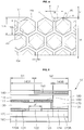
- FIG. 1 is a plan view of an optical display according to one embodiment of the present disclosure.
- FIG. 2 is a partial cross-sectional view of the optical display of FIG. 1 , taken along line I-II.
- FIG. 3 is a partial cross-sectional view of a first polarizing plate according to one embodiment of the present disclosure.
- FIG. 4 is an enlarged cross-sectional view of a printed pattern at (e.g., formed at) the interface between a display region and a non-display region of a light shielding layer in region PI of the optical display of FIG. 1 .
- FIG. 5 is a partial cross-sectional view of an optical display according to another embodiment of the present disclosure.
- FIG. 1 is a plan view of an optical display according to one embodiment of the present disclosure.
- FIG. 2 is a partial cross-sectional view of the optical display of FIG. 1 , taken along line I-II.
- the optical display 10 may include: a display region S 1 ; and a non-display region S 2 along (e.g., formed along a periphery of the display region S 1 .
- the non-display region S 2 is shown as surrounding the entire periphery of the display region S 1 in FIG. 1 , it should be understood that the present disclosure is not limited thereto.
- the non-display region may be located only at right and left sides of the display region, or may be located only at one selected from right, left, upper, and lower sides of the display region.
- the frame is shown as being on (e.g., formed on) one surface of the optical display in FIG. 1 , it should be understood that the present disclosure is not limited thereto and, for example, the optical display may have a frameless structure.
- a support may be coupled to (e.g., connected to) the optical display via the side surface of the optical display, for example, the frame, to support the optical display.
- the optical display is shown as including the liquid crystal panel as an optical display element in FIG. 2 , it should be understood that the present disclosure is not limited thereto.
- the optical display may include a light emitting diode substrate containing a luminous material, as an optical display element.
- the liquid crystal panel may include a first substrate 110 , the second substrate 120 under (e.g., formed under) the first substrate 110 and facing the first substrate 110 , and a liquid crystal layer 130 between (e.g., formed between) the first substrate 110 and the second substrate 120 .
- the liquid crystal layer 130 may include a liquid crystal that is uniformly oriented when an electric field is not applied thereto.
- the liquid crystal layer may employ a vertical alignment (VA) mode, a patterned vertical alignment (PVA) mode, or a super-patterned vertical alignment (S-PVA) mode, without being limited thereto.
- VA vertical alignment
- PVA patterned vertical alignment
- S-PVA super-patterned vertical alignment
- the liquid crystal layer 130 may optionally further include a sealing layer 131 at both ends thereof to prevent the liquid crystal from flowing out or from being contaminated by external moisture (or to reduce a likelihood or amount of the liquid crystal flowing out or the likelihood or amount of contamination by external moisture).
- the liquid crystal layer may optionally further include a spacer to achieve a space allowing the liquid crystal layer to have a set (e.g., predetermined) thickness.
- the first substrate 110 may be on (e.g., formed on) one surface of the liquid crystal layer 130 to support the liquid crystal layer 130 .
- the first substrate 110 is a color filter substrate and may support a color filter layer 111 on (e.g., formed on) a lower surface of the first substrate 110 .
- the color filter layer 111 may extract three light components of red (R), green (G), and blue (B) emitted from a plurality of pixels in (e.g., formed in) the display region S 1 of the second substrate 120 , thereby implementing the desired colors on the optical display.
- the color filter layer 111 may employ any suitable configuration generally used in the art.
- the color filter layer 111 may be in (e.g., formed in) at least a portion of the display region S 1 of the optical display to extract light emitted from (or transmitted through) the liquid crystal layer 130 .
- the color filter layer may be on (e.g., formed on) at least a portion of the lower surface of the first substrate.
- the color filter layer 111 may be on (e.g., formed on) only a portion of the lower surface of the first substrate 110 , as shown in FIG. 2 .
- the color filter layer may be on the entire (or substantially entire) lower surface of the first substrate.
- the first substrate 110 may include an insulating material such as glass, polymers, or stainless steel. Any suitable glass, polymer, and/or stainless steel generally used in the art may be used as a material for the first substrate 110 .
- the first substrate 110 may be flexible or may not be flexible.
- an electrode film for transmitting signals such as an indium tin oxide (ITO) film
- an alignment film for aligning the liquid crystal in the liquid crystal layer may also be on (e.g., formed on) the lower surface of the first substrate 110 .
- the second substrate 120 may be on (e.g., formed on) the other surface of the liquid crystal layer 130 to support the liquid crystal layer 130 .
- the second substrate 120 may be a TFT substrate.
- a pixel region 121 having a plurality of TFTs arranged therein and a metal interconnection layer 123 ; 124 coupled to (e.g., connected to) the TFTs may be formed.
- a dummy region 122 may be between the pixel region 121 and the metal interconnection layer 123 ; 124 .
- the second substrate 120 extends beyond the first substrate 110 .
- the second substrate 120 includes a main body 120 A and an extended portion 120 B directly coupled to (e.g., directly connected to) the main body 120 A.
- the main body 120 A may face the first substrate 110 .
- the extended portion 120 B does not face the first substrate 110 .
- the pixel region 121 on (e.g., formed on) the upper surface of the second substrate 120 includes the plurality of TFTs arranged therein and constitutes at least a portion of the display region. In some embodiments, the pixel region 121 constitutes or defines the display region S 1 .
- the pixel region 121 may include a plurality of pixels R, G, B, gate lines coupled to (e.g., connected to) the plurality of pixels R, G, B, and data lines coupled to (e.g., connected to) the plurality of pixels R, G, B.
- the plurality of pixels R, G, B are located in the display region S 1 of the pixel region 121 and may be arranged in a matrix in column and row directions.
- the plurality of pixels are respectively located at intersections of the gate lines and the data lines.
- Each pixel includes a TFT including a gate, an active layer, a source, and a drain.
- the gate lines are arranged at substantially regular intervals and each gate line extends along the row direction.
- the plurality of pixels R, G, B adjacent to one another in the row direction may be coupled to (e.g., connected to) the same gate line.
- the data lines are arranged at substantially regular intervals and each data line extends along the column direction.
- the plurality of pixels R, G, B may be respectively coupled to (e.g., connected to) the gate lines and the data lines through the TFTs. When a gate-on voltage is applied to the gate lines, the TFTs are turned on, such that data signals are respectively applied to the pixels through the data lines.
- the dummy region 122 including dummy wires coupled (e.g., connected) between the gate lines and the data lines in the pixel region 121 may be adjacent to the pixel region 121 .
- the dummy region 122 may optionally constitute a portion of the display region S 1 and a portion of the non-display region S 2 .
- a portion of the dummy region 122 may be in the display region S 1 and another portion of the dummy region 122 may be in the non-display region S 2 .
- the metal interconnection layer 123 ; 124 may be adjacent to the dummy region 122 .
- the metal interconnection layer 123 ; 124 includes a first metal interconnection layer 123 on (e.g., formed on) the main body 120 A of the second substrate 120 and a second metal interconnection layer 124 on (e.g., formed on) the extended portion 120 B of the second substrate 120 .
- the first metal interconnection layer 123 and the second metal interconnection layer 124 are coupled to (e.g., connected to) each other and may each constitute or define the non-display region S 2 .
- the first metal interconnection layer 123 is a layer in which various metal wires extending from the pixel region 121 and the dummy region 122 exist together, and may include a driving integrated circuit (driving IC).
- the second metal interconnection layer 124 may couple (e.g., connect) the first metal interconnection layer 123 to a printed circuit board (PCB).
- PCB printed circuit board
- connection between the first metal interconnection layer 123 and the PCB may be achieved by a chip-on-film (COF) process, a chip-on-glass (COG) process, a tape carrier package (TCP) process, and/or the like.
- COF chip-on-film
- COG chip-on-glass
- TCP tape carrier package
- the second metal interconnection layer 124 may be coupled to (e.g., connected to) the first metal interconnection layer 123 through an anisotropic conductive film (ACF), without being limited thereto.
- ACF anisotropic conductive film
- a bonding layer (for example, a sealing layer) may also be on (e.g., formed on) the upper surface of the second metal interconnection layer 124 to prevent the second metal interconnection layer 124 from being separated from the first metal interconnection layer 123 or the liquid crystal layer 130 (or to reduce a likelihood or degree of such separation).
- An electrode film for transmitting signals such as an indium tin oxide (ITO) film, and an alignment film for aligning the liquid crystal in the liquid crystal layer may also be on (e.g., formed on) the upper surface of the second substrate 120 .
- ITO indium tin oxide
- the second substrate 120 may include a material which is the same as or different from the material for the first substrate 110 as set forth above.
- the first polarizing plate 140 may be on (e.g., formed on) one surface of the liquid crystal panel, for example, on the upper surface (the light exit surface) of the first substrate 110 to polarize light from the liquid crystal panel and emit or transmit the polarized light.
- the first polarizing plate 140 may extend beyond the first substrate 110 .
- the first polarizing plate 140 may include a main body 140 A and an extended portion 140 B directly coupled to (e.g., directly connected to) the main body 140 A.
- the main body 140 A may face the first substrate 110 .
- the extended portion 140 B does not face the first substrate 110 . Instead, the extended portion 140 B faces the extended portion 120 B of the second substrate 120 .
- the first polarizing plate 140 includes a light shielding layer 150 therein (e.g., formed therein), wherein the light shielding layer 150 may constitute or define the non-display region S 2 .
- the light shielding layer 150 may be in (e.g., formed in) the extended portion 1408 of the first polarizing plate 140 and a portion of the main body 140 A of the first polarizing plate 140 .
- a portion of the light shielding layer 150 may be in the extended portion 140 B of the first polarizing plate 140 and another portion of the light shielding layer 150 may be in the portion of the main body 140 A of the first polarizing plate 140 .
- the light shielding layer can prevent the metal interconnection layer from being visible (or can reduce the visibility of the metal interconnection layer to the outside of the optical display) or prevent the metal interconnection layer and at least a portion of the dummy region from being visible (or reduce the visibility of the metal interconnection layer and at least a portion of the dummy region to the outside of the optical display).
- the light shielding layer may be in (e.g., formed in) the first polarizing plate to face the metal interconnection layer (the first metal interconnection layer and the second metal interconnection layer) and a portion of the dummy region on the second substrate, thereby preventing the metal interconnection layer and the portion of the dummy region on the second substrate from being visible (or reducing the visibility of the metal interconnection layer and the portion of the dummy region on the second substrate to the outside of the optical display).
- the light shielding layer may be in (e.g., formed in) the first polarizing plate to face the metal interconnection layer (the first metal interconnection layer and the second metal interconnection layer) and the dummy region on the second substrate, thereby preventing the metal interconnection layer and the dummy region on the second substrate from being visible (or reducing the visibility of the metal interconnection layer and the portion of the dummy region on the second substrate to the outside of the optical display).
- the metal interconnection layer is hidden by the light shielding layer 150 , such that reflectance of the metal interconnection layer can be reduced, thereby improving visibility of the optical display.
- FIG. 3 is a partial cross-sectional view of a first polarizing plate according to one embodiment of the present disclosure.
- the first polarizing plate 140 may include: a polarizer 141 ; a bonding layer 144 and a first polarizer protective film 142 sequentially stacked on one surface of the polarizer 141 ; a second polarizer protective film 143 stacked on the other surface of the polarizer 141 ; and a light shielding layer 150 on (e.g., formed on) one surface of the first polarizer protective film 142 and embedded in the bonding layer 144 . Since the light shielding layer 150 is embedded in the bonding layer 144 , the overall thickness of the optical display can be reduced.
- the thickness of the light shielding layer 150 may be less than or equal to that of the bonding layer 144 . In one embodiment, the thickness of the light shielding layer may be in a range of about 50% to about 100% that of the bonding layer. Within this range, the light shielding layer 150 can be embedded in the bonding layer, thereby reducing the overall thickness of the polarizing plate.
- the light shielding layer may have a thickness of about 4 ⁇ m or less, for example, about 0.1 ⁇ m to about 4 ⁇ m, or about 1 ⁇ m to about 4 ⁇ m.
- the light shielding layer 150 serves to block or absorb light and may include a set or specific design such as a logo of a company or a dot pattern. In other words, the light shielding layer may include a design providing aesthetic appeal to the optical display, thereby improving consumer preference.
- the light shielding layer 150 may be formed from a composition for light shielding layers described herein below to have adhesion to the first polarizer protective film, thereby allowing the polarizer to be coupled to the first polarizer protective film. In this way, the polarizer can be coupled to the first polarizer protective film without a separate bonding layer between the polarizer and the light shielding layer and between the first polarizer protective film and the light shielding layer.
- the composition for forming the light shielding layer may include a pigment, a binder resin, and an initiator and may further include at least one of a reactive unsaturated compound, a solvent, and an additive.
- the pigment may include carbon black, a mixed pigment of silver-tin alloys (e.g., a mixed pigment including a silver-tin alloy), or a combination thereof.
- carbon black may include graphitized carbon, furnace black, acetylene black, and Ketjen black, without being limited thereto.
- the pigment may be used in the form of a pigment dispersion, without being limited thereto.
- the binder resin may include an acrylic resin, a polyimide resin, a polyurethane resin, or a combination thereof.
- the acrylic resin may include a methacrylic acid/benzyl methacrylate copolymer, a methacrylic acid/benzyl methacrylate/styrene copolymer, a methacrylic acid/benzyl methacrylate/2-hydroxyethyl methacrylate copolymer, and a methacrylic acid/benzyl methacrylate/styrene/2-hydroxyethyl methacrylate copolymer.
- the polyurethane resin may be an aliphatic polyurethane resin.
- the acrylic resin may be an acrylic pressure-sensitive adhesive resin. However, it should be understood that the present disclosure is not limited thereto.
- the reactive unsaturated compound has a lower weight average molecular weight than the binder resin and may include at least one of a photocurable unsaturated compound and a heat-curable unsaturated compound.
- the reactive unsaturated compound may include ethylene glycol diacrylate, ethylene glycol dimethacrylate, diethylene glycol diacrylate, triethylene glycol diacrylate, triethylene glycol dimethacrylate, 1,6-hexanediol diacrylate, 1,6-hexanediol dimethacrylate, pentaerythritol tri(meth)acrylate, pentaerythritol tetra(meth)acrylate, dipentaerythritol penta(meth)acrylate, dipentaerythritol hexa(meth)acrylate, bisphenol A epoxy (meth)acrylate, ethylene glycol monomethyl ether (meth)acrylate, trimethylol propane tri(meth)acrylate, and tris(
- the initiator may include at least one of a photopolymerization initiator and a heat-curing initiator.
- a photopolymerization initiator may include acetophenone compounds, benzophenone compounds, thioxanthone compounds, benzoin compounds, triazine compounds, and morpholine compounds, without being limited thereto.
- the heat-curing initiator may include at least one selected from the group consisting of: hydrazide compounds such as 1,3-bis(hydrazinocarbonoethyl-5-isopropylhydantoin); imidazole compounds such as 1-cyanoethyl-2-phenylimidazole, N-[2-(2-methyl-1-imidazolyl)ethyl]urea, 2,4-diamino-6-[2′-methylimidazolyl-(1′)]-ethyl-s-triazine, N,N′-bis(2-methyl-1-imidazolylethyl)urea, N,N′-(2-methyl-1-imidazolylethyl)-adipamide, 2-phenyl-4-methyl-5-hydroxymethylimidazole, and 2-phenyl-4,5-dihydroxymethylimidazole; acid anhydride compounds such as tetrahydrophthalic anhydride, ethylene glycol-bis(anhydrotrimell
- the solvent may include: glycol ethers such as ethylene glycol methyl ether, ethylene glycol ethyl ether, and propylene glycol methyl ether; cellosolve acetates such as methyl cellosolve acetate, ethyl cellosolve acetate, and diethyl cellosolve acetate; carbitols such as methylethyl carbitol, diethyl carbitol, diethylene glycol monomethyl ether, diethylene glycol monoethyl ether, diethylene glycol dimethyl ether, diethylene glycol methylethyl ether, and diethylene glycol diethyl ether; and propylene glycol alkyl ether acetates such as propylene glycol methyl ether acetate and propylene glycol propyl ether acetate, without being limited thereto.
- glycol ethers such as ethylene glycol methyl ether, ethylene glycol ethyl ether, and prop
- the composition for forming the light shielding layer may include about 1 wt % to about 50 wt % of the pigment (or the pigment dispersion), about 0.5 wt % to about 20 wt % of the binder resin, about 0.1 wt % to about 10 wt % of the initiator, and the balance of the solvent.
- the light shielding layer can have (e.g., be formed to have) a slim (e.g., thin) structure while achieving a good light shielding effect.
- the composition for light shielding layers may include about 1 wt % to about 50 wt % of the pigment (or the pigment dispersion), about 0.5 wt % to about 20 wt % of the binder resin, about 0.1 wt % to about 20 wt % of the reactive unsaturated compound, about 0.1 wt % to about 10 wt % of the initiator, and the balance of the solvent.
- the light shielding layer can have (e.g., be formed to have) a slim (e.g., thin) structure while achieving a good light shielding effect.
- the composition for light shielding layers may further include about 0.1 wt % to about 1 wt % of other additives.
- the additive may include a silane coupling agent, which serves to promote curing of the light shielding layer through UV irradiation.
- the light shielding layer 150 is interposed between the first polarizer protective film 142 and the polarizer 141 in FIG. 3 , it should be understood that the present disclosure is not limited thereto, and the light shielding layer 150 may be interposed between the second polarizer protective film 143 and the polarizer 141 .
- the polarizer 141 , the first polarizer protective film 142 , the second polarizer protective film 143 , and the bonding layer 144 may include any suitable ones available in the art.
- FIG. 4 is an enlarged view of a printed pattern formed at the interface between the display region and the non-display region of the light shielding layer in region PI of the optical display of FIG. 1 .
- the printed pattern may be formed over the entire (or substantially entire) light shielding layer, including the interface between the display region and the non-display region of the light shielding layer.
- the light shielding layer may include a printed region composed of a plurality of printed patterns 153 .
- the rest of the light shielding layer corresponds to a non-printed region 154 .
- the printed patterns 153 are separated from one another.
- Each of the printed patterns 153 includes: a first printed layer 151 ; and a second printed layer 152 directly formed on (or directly on) the first printed layer 151 .
- the second printed layer 152 may have a different shape than the first printed layer 151 to provide the light shielding effect even when the light shielding layer is formed to have a slim (e.g., thin) structure.
- the present disclosure is not limited thereto and the second printed layer 152 may have the same (e.g., substantially the same) shape as the first printed layer 151 .
- the second printed layers 152 may have a smaller unit area than the first printed layers 151 .
- the number of the second printed layers 152 per unit area of the non-display region may be greater than that of the first printed layers 151 .
- a point at which one first printed layer 151 adjoins the interface between the display region S 1 and the non-display region S 2 is indicated by Point a
- a point at which another first printed layer 151 adjacent to the one first printed layer 151 adjoins the interface between the display region S 1 and the non-display region S 2 is indicated by Point b.
- the closest vertex or inflection point of the one first printed layer 151 to Point a is indicated by Point c
- the closest vertex or inflection point of the other first printed layer 151 to Point b is indicated by Point d.
- H A minimum value among the distance from the interface between the display region S 1 and the non-display region S 2 to Point c and the distance from the interface between the display region S 1 and the non-display region S 2 to Point d is indicated by H.
- H may be about 200 ⁇ m or less, for example, about 0.1 ⁇ m to about 200 ⁇ m or about 5 ⁇ m to about 200 ⁇ m.
- the light shielding layer can achieve the light shielding effect and uniformity between the display region and the non-display region can be improved to reduce a visibility difference therebetween while preventing the plurality of pixels R, G, B from being visible (or while reducing the visibility of the plurality of pixels R, G, B to the outside of the optical display).
- interface between the display region and the non-display region refers to an (imaginary) line connecting points of the first printed layers in (e.g., formed in) the non-display region, which are closest to the display region.
- the shortest distance ⁇ L between Point a and Point a′ may be about 200 ⁇ m or less, for example, about 0.1 ⁇ m to about 200 ⁇ m or about 10 ⁇ m to about 200 ⁇ m.
- the light shielding layer can achieve the light shielding effect and uniformity between the display region and the non-display region can be improved to reduce a visibility difference therebetween.
- a difference in length between a maximum major axis 151 L of the first printed layer 151 and a maximum major axis 152 L of the second printed layer 152 may be about 200 ⁇ m or less, for example, about 0.1 ⁇ m to about 200 ⁇ m or about 10 ⁇ m to about 200 ⁇ m.
- the light shielding layer can achieve the light shielding effect and uniformity between the display region and the non-display region can be improved to reduce a visibility difference therebetween while preventing the plurality of pixels R, G, B from being visible (or reducing the visibility of the plurality of pixels R, G, B to the outside of the optical display).
- the maximum major axis 151 L of the first printed layer 151 may have a length of about 50 ⁇ m to about 600 ⁇ m, for example, about 100 ⁇ m to about 500 ⁇ m and the maximum major axis 152 L of the second printed layer 152 may have a length of about 50 ⁇ m to about 500 ⁇ m, for example, about 50 ⁇ m to about 350 ⁇ m.
- W may range from about 10 ⁇ m to about 500 ⁇ m, for example, about 10 ⁇ m to about 490 ⁇ m or about 10 ⁇ m to about 480 ⁇ m.
- W may be greater than H (W>H).
- the printed pattern may satisfy Relation 1: about 0.1 ⁇ W ⁇ H ⁇ about 0.5 ⁇ W.
- Relation 1 is set or designed to achieve uniformity at the interface between the display region and the non-display region in order to achieve uniformity of the first printed layer directly adjoining the interface between the display region and the non-display region.
- the first printed layer 151 may have a regular hexagonal shape and the second printed layer 152 may have a rhombic shape.
- the first printed layer 151 may have an n-gonal shape (n being an integer of 3 to 10) such as a hexagonal shape (when n is 6), a circular shape, an elliptical shape, or an amorphous shape
- the second printed layer 152 may have an n-gonal shape (n being an integer of 3 to 10) such as a hexagonal shape (when n is 6), a circular shape, an elliptical shape, or an amorphous shape.
- Sides constituting the first printed layer 151 may have the same or different lengths.
- each of the sides constituting the first printed layer 151 may have a length of about 10 ⁇ m to about 400 ⁇ m, for example, about 50 ⁇ m to about 300 ⁇ m.
- Sides constituting the second printed layer 152 may have the same or different lengths.
- each of the sides constituting the second printed layer 151 may have a length of about 10 ⁇ m to about 400 ⁇ m, for example, about 50 ⁇ m to about 300 ⁇ m.
- the length of one side constituting the first printed layer 151 may be the same as or different from the length of one side constituting the second printed layer 152 . In some embodiments, the length of one side constituting the first printed layer 151 is the same (e.g., substantially the same) as the length of one side constituting the second printed layer 152 .
- the first printed layer may have a regular hexagonal shape and may be arranged in a honeycomb shape
- the second printed layer may have a rhombic, square, or amorphous shape.
- the second printed layer may have a smaller area than the first printed layer.
- the second printed layer can be on (e.g., formed on) the first printed layer.
- the number of intersection points between the first printed layer and the second printed layer may be at least two, for example, three or more.
- the term “intersection point” may refer to a point of intersection of the periphery of the first printed layer 151 and the periphery of the second printed layer 152 , as shown in FIG. 4 .
- the light shielding layer can achieve high uniformity between the display region and the non-display region, thereby reducing a visibility difference therebetween while preventing R, G, B in the pixel from being visible (or thereby reducing the visibility of R, G, and B in the pixel to the outside of the optical display).
- the second printed layers 152 may have a smaller or larger unit area than the first printed layers 151 .
- the number of the second printed layers 152 per unit area of the non-display region may be larger or smaller than that of the first printed layers 151 .
- a distance T between a pair of adjacent printed patterns 153 may range from about 1 ⁇ m to about 50 ⁇ m, for example, about 5 ⁇ m to about 30 ⁇ m. Within these ranges, the light shielding layer can exhibit light shielding properties without (or substantially without) adversely affecting uniformity between the display region and the non-display region.
- the first printed layer 151 may have the same (e.g., substantially the same) thickness as or a different from that of the second printed layer 152 .
- Each of the first printed layer 151 and the second printed layer 152 may have a thickness of about 4 ⁇ m or less, for example, about 0.1 ⁇ m to less than about 4 ⁇ m.
- the light shielding layer can be formed inside the bonding layer, thereby allowing a reduction in thickness of the polarizing plate while achieving light shielding properties, as compared to a polarizing plate that does not include a light shielding layer embedded therein.
- the printed pattern is shown as having a bilayer structure of the first printed layer 151 and the second printed layer 152 .
- the present disclosure is not limited thereto and the printed pattern may have a monolayer structure or a multilayer structure of, for example, three or more layers.
- the first printed layer 151 is shown as a lowermost printed layer of the printed pattern, which directly contacts the first polarizer protective film 142 .
- the present disclosure is not limited thereto and the first printed layer 151 may be formed between other printed layers without contacting the first polarizer protective film 142 .
- the second polarizing plate 160 may be on (e.g., formed on) the other surface of the liquid crystal panel to polarize light from a light source and emit the polarized light to the liquid crystal panel.
- the second polarizing plate 160 may include a polarizer and a protective film on (e.g., formed on) at least one surface of the polarizer.
- the polarizer and the protective film may include any suitable ones available in the art.
- first polarizing plate 140 and the second polarizing plate 160 may be secured to the first substrate and the second substrate, respectively, using any suitable adhesive or bonding agent available in the art.
- a securing member 170 may be in (e.g., formed in) a region surrounded by (e.g., defined by) the first polarizing plate 140 , the first substrate 110 , the liquid crystal layer 130 , and the second substrate 120 .
- the securing member 170 may contact the first polarizing plate 140 , the first substrate 110 , the liquid crystal layer 130 , and the second substrate 120 .
- the securing member 170 contacts the extended portion 110 B of the first substrate 110 and the extended portion 120 B of the second substrate 120 .
- the securing member may completely (e.g., substantially completely) fill the region surrounded by the first polarizing plate, the first substrate, the liquid crystal layer, and the second substrate.
- the securing member 170 serves to secure the first polarizing plate 140 , for example, the extended portion 140 B of the first polarizing plate 140 , to the first substrate 110 , the liquid crystal layer 130 , and the second substrate 120 to allow the first polarizing plate to remain firmly secured when the first polarizing plate shrinks or expands due to shrinkage or expansion of the polarizer under high temperature and/or high temperature and high humidity conditions, thereby preventing the polarizing plate and the light shielding layer from suffering from deformation (or reducing a likelihood or degree of such deformation), such as wrinkling, while allowing the first polarizing plate, which extends beyond the first substrate, to retain the original shape thereof.
- the metal interconnection layer can be visible or display visibility of the optical display can be deteriorated.
- the securing member prevents or reduces deformation of the light shielding layer due to shrinkage or expansion of the polarizer, thereby allowing the metal interconnection layer to be kept invisible (or thereby reducing the visibility of the metal interconnection layer to the outside of the optical display).
- the securing member 170 may be formed by applying an adhesive film, such as an optically clear adhesive (OCA) or a pressure sensitive adhesive (PSA), to a set (e.g., predetermined) thickness, or by injecting a sealing agent into the region.
- the sealing agent may include a powder such as silica, without being limited thereto.
- the silica may be SEAHOSTAR KE-S series (e.g., S100) produced by Nippon Shokubai Co., Ltd., without being limited thereto.
- the securing member 170 is shown as contacting the first polarizing plate 140 , the first substrate 110 , the liquid crystal layer 130 , and the second substrate 120 .
- the present disclosure is not limited thereto and the securing member may contact only the first polarizing plate and at least a portion of the first substrate or may contact the first polarizing plate, the first substrate, and at least a portion of the liquid crystal layer, so long as the securing member can suppress or reduce deformation of the polarizing plate and the light shielding layer.
- an optical display 10 ′ according to this embodiment is substantially the same as the optical display 10 according to the above embodiment except that a black matrix layer 190 is further on (e.g., formed on) a lower surface of a first substrate 110 .
- a color filter layer 111 and the black matrix layer 190 are located (e.g., formed).
- the color filter layer 111 may be on (e.g., formed on) a portion of the lower surface of the first substrate 110 and the black matrix layer 190 may be separated from an outer peripheral surface of the color filter layer 111 , without being limited thereto.
- the color filter layer 111 corresponds to (e.g., is formed to correspond to) the display region S 1 and the black matrix layer 190 corresponds to (e.g., is formed to correspond to) the non-display region S 2 .
- the black matrix layer 190 serves to further prevent or reduce reflection on surfaces of the wires and prevent or reduce light leakage.
- the black matrix layer 190 may be formed from the composition for light shielding layers as set forth above or any suitable black matrix layer available in the art.
- the present disclosure provides an optical display that can conceal a metal interconnection layer and the like without a decorative frame.
- the present disclosure provides an optical display that includes a TFT substrate extending beyond a color filter substrate such that a metal interconnection layer is on the extended portion of the TFT substrate, while concealing the metal interconnection layer without a decorative frame.
- the present disclosure provides an optical display free from any decorative frame exposed outside the optical display, thereby having good appearance.
- Embodiments of the present disclosure provides an optical display which can prevent a polarizing plate and/or a light shielding layer from suffering from deformation (or reduce a likelihood or degree of such deformation), such as wrinkling, due to shrinkage or expansion of a polarizer under high temperature and/or high temperature and high humidity conditions.
- Embodiments of the present disclosure provides an optical display which can minimize or reduce difference in visibility between a display region and a non-display region.
- the terms “substantially,” “about,” and similar terms are used as terms of approximation and not as terms of degree, and are intended to account for the inherent deviations in measured or calculated values that would be recognized by those of ordinary skill in the art. Further, the use of “may” when describing embodiments of the present disclosure refers to “one or more embodiments of the present disclosure.” As used herein, the terms “use,” “using,” and “used” may be considered synonymous with the terms “utilize,” “utilizing,” and “utilized,” respectively. Also, the term “exemplary” is intended to refer to an example or illustration.
- any numerical range recited herein is intended to include all sub-ranges of the same numerical precision subsumed within the recited range.
- a range of “1.0 to 10.0” is intended to include all subranges between (and including) the recited minimum value of 1.0 and the recited maximum value of 10.0, that is, having a minimum value equal to or greater than 1.0 and a maximum value equal to or less than 10.0, such as, for example, 2.4 to 7.6.
- Any maximum numerical limitation recited herein is intended to include all lower numerical limitations subsumed therein, and any minimum numerical limitation recited in this specification is intended to include all higher numerical limitations subsumed therein. Accordingly, Applicant reserves the right to amend this specification, including the claims, to expressly recite any sub-range subsumed within the ranges expressly recited herein.
Landscapes
- Physics & Mathematics (AREA)
- Nonlinear Science (AREA)
- Mathematical Physics (AREA)
- Chemical & Material Sciences (AREA)
- Crystallography & Structural Chemistry (AREA)
- General Physics & Mathematics (AREA)
- Optics & Photonics (AREA)
- Liquid Crystal (AREA)
- Devices For Indicating Variable Information By Combining Individual Elements (AREA)
Abstract
Description
Claims (24)
Applications Claiming Priority (2)
| Application Number | Priority Date | Filing Date | Title |
|---|---|---|---|
| KR1020170177600A KR102112870B1 (en) | 2017-12-21 | 2017-12-21 | Optical display apparatus |
| KR10-2017-0177600 | 2017-12-21 |
Publications (2)
| Publication Number | Publication Date |
|---|---|
| US20190196256A1 US20190196256A1 (en) | 2019-06-27 |
| US10627665B2 true US10627665B2 (en) | 2020-04-21 |
Family
ID=66951077
Family Applications (1)
| Application Number | Title | Priority Date | Filing Date |
|---|---|---|---|
| US16/205,118 Active US10627665B2 (en) | 2017-12-21 | 2018-11-29 | Optical display |
Country Status (4)
| Country | Link |
|---|---|
| US (1) | US10627665B2 (en) |
| KR (1) | KR102112870B1 (en) |
| TW (1) | TWI695192B (en) |
| WO (1) | WO2019124754A1 (en) |
Cited By (1)
| Publication number | Priority date | Publication date | Assignee | Title |
|---|---|---|---|---|
| US10908337B2 (en) * | 2017-12-21 | 2021-02-02 | Samsung Sdi Co., Ltd. | Polarizing plate and optical display comprising the same |
Families Citing this family (7)
| Publication number | Priority date | Publication date | Assignee | Title |
|---|---|---|---|---|
| CN110824750A (en) * | 2019-11-20 | 2020-02-21 | 京东方科技集团股份有限公司 | a display device |
| KR102753710B1 (en) * | 2020-06-26 | 2025-01-10 | 엘지디스플레이 주식회사 | Transparent display device |
| CN111708206B (en) * | 2020-07-17 | 2024-03-26 | 合肥鑫晟光电科技有限公司 | Touch display module, manufacturing method thereof and display device |
| CN114185195A (en) * | 2021-12-10 | 2022-03-15 | 苏州华星光电技术有限公司 | Display device |
| CN114265223B (en) * | 2021-12-20 | 2022-10-21 | 绵阳惠科光电科技有限公司 | Display panel and display device |
| CN116321824A (en) * | 2021-12-21 | 2023-06-23 | 群创光电股份有限公司 | Electronic device |
| JP7733416B2 (en) * | 2022-03-30 | 2025-09-03 | パナソニックオートモーティブシステムズ株式会社 | display device |
Citations (11)
| Publication number | Priority date | Publication date | Assignee | Title |
|---|---|---|---|---|
| TWM356139U (en) | 2008-12-30 | 2009-05-01 | Mildex Optical Inc | Touch panel with light adjustment function |
| KR20090122092A (en) | 2008-05-23 | 2009-11-26 | 엘지디스플레이 주식회사 | LCD and its manufacturing method |
| KR20100001275A (en) | 2008-06-26 | 2010-01-06 | 삼성모바일디스플레이주식회사 | Organic light emitting diode display and method for manufacturing the smae |
| KR20120056519A (en) | 2010-11-25 | 2012-06-04 | 엘지디스플레이 주식회사 | Sealant for heat hardening and method for fabricating liquid crystal display panel |
| KR20150015243A (en) | 2013-07-31 | 2015-02-10 | 엘지디스플레이 주식회사 | Liquid crystal display having a narrow bezel |
| KR20160038559A (en) | 2014-09-30 | 2016-04-07 | 엘지디스플레이 주식회사 | Display Device |
| US20160327828A1 (en) * | 2015-05-08 | 2016-11-10 | Japan Display Inc. | Liquid crystal display device |
| US20160363795A1 (en) | 2015-06-10 | 2016-12-15 | Samsung Display Co., Ltd. | Display panel and display device including the same |
| KR20170086780A (en) | 2016-01-19 | 2017-07-27 | 삼성에스디아이 주식회사 | Polarizer plate and display device comprising the same |
| US20190278143A1 (en) * | 2011-08-09 | 2019-09-12 | Japan Display Inc. | Liquid crystal display apparatus |
| US20190278117A1 (en) * | 2016-09-13 | 2019-09-12 | Infovision Optoelectronics (Kunshan) Co., Ltd. | Liquid crystal display device with switchable viewing angle and viewing angle switching method |
Family Cites Families (3)
| Publication number | Priority date | Publication date | Assignee | Title |
|---|---|---|---|---|
| KR102116443B1 (en) * | 2013-09-02 | 2020-05-28 | 엘지디스플레이 주식회사 | Display device and method for manufacturing of the same |
| JP6611508B2 (en) * | 2015-08-05 | 2019-11-27 | 三菱電機株式会社 | Display device |
| KR102455580B1 (en) * | 2015-12-31 | 2022-10-17 | 엘지디스플레이 주식회사 | Display Device |
-
2017
- 2017-12-21 KR KR1020170177600A patent/KR102112870B1/en active Active
-
2018
- 2018-11-16 WO PCT/KR2018/014130 patent/WO2019124754A1/en not_active Ceased
- 2018-11-29 US US16/205,118 patent/US10627665B2/en active Active
- 2018-12-03 TW TW107143214A patent/TWI695192B/en active
Patent Citations (12)
| Publication number | Priority date | Publication date | Assignee | Title |
|---|---|---|---|---|
| KR20090122092A (en) | 2008-05-23 | 2009-11-26 | 엘지디스플레이 주식회사 | LCD and its manufacturing method |
| KR20100001275A (en) | 2008-06-26 | 2010-01-06 | 삼성모바일디스플레이주식회사 | Organic light emitting diode display and method for manufacturing the smae |
| TWM356139U (en) | 2008-12-30 | 2009-05-01 | Mildex Optical Inc | Touch panel with light adjustment function |
| KR20120056519A (en) | 2010-11-25 | 2012-06-04 | 엘지디스플레이 주식회사 | Sealant for heat hardening and method for fabricating liquid crystal display panel |
| US20190278143A1 (en) * | 2011-08-09 | 2019-09-12 | Japan Display Inc. | Liquid crystal display apparatus |
| KR20150015243A (en) | 2013-07-31 | 2015-02-10 | 엘지디스플레이 주식회사 | Liquid crystal display having a narrow bezel |
| CN104345492A (en) | 2013-07-31 | 2015-02-11 | 乐金显示有限公司 | Display device |
| KR20160038559A (en) | 2014-09-30 | 2016-04-07 | 엘지디스플레이 주식회사 | Display Device |
| US20160327828A1 (en) * | 2015-05-08 | 2016-11-10 | Japan Display Inc. | Liquid crystal display device |
| US20160363795A1 (en) | 2015-06-10 | 2016-12-15 | Samsung Display Co., Ltd. | Display panel and display device including the same |
| KR20170086780A (en) | 2016-01-19 | 2017-07-27 | 삼성에스디아이 주식회사 | Polarizer plate and display device comprising the same |
| US20190278117A1 (en) * | 2016-09-13 | 2019-09-12 | Infovision Optoelectronics (Kunshan) Co., Ltd. | Liquid crystal display device with switchable viewing angle and viewing angle switching method |
Non-Patent Citations (2)
| Title |
|---|
| Korean Office Action dated Oct. 29, 2019 in corresponding Korean Patent Application No. 10-2017-0177600 (7 pgs.). |
| Taiwan Office action dated Sep. 18, 2019 from corresponding Taiwan Patent Application No. 107143214 (9 pgs.). |
Cited By (1)
| Publication number | Priority date | Publication date | Assignee | Title |
|---|---|---|---|---|
| US10908337B2 (en) * | 2017-12-21 | 2021-02-02 | Samsung Sdi Co., Ltd. | Polarizing plate and optical display comprising the same |
Also Published As
| Publication number | Publication date |
|---|---|
| TW201928408A (en) | 2019-07-16 |
| KR102112870B1 (en) | 2020-05-19 |
| KR20190075758A (en) | 2019-07-01 |
| US20190196256A1 (en) | 2019-06-27 |
| WO2019124754A1 (en) | 2019-06-27 |
| TWI695192B (en) | 2020-06-01 |
Similar Documents
| Publication | Publication Date | Title |
|---|---|---|
| US10627665B2 (en) | Optical display | |
| KR102563743B1 (en) | Protecting cover and display device comprising thereof | |
| US20140293574A1 (en) | Display apparatus | |
| KR102112864B1 (en) | Polarizing plate and optical display device comprising the same | |
| JP6603154B2 (en) | Display device and electronic device | |
| CN102087436A (en) | Liquid crystal display | |
| CN102177538A (en) | Display device and method for manufacturing the same | |
| US9626053B2 (en) | Touch control display device and joint touch control display | |
| KR20130106731A (en) | Display panel and display apparatus having the same | |
| CN104216155A (en) | Display unit | |
| US20170139100A1 (en) | Backlight unit and display device including the same | |
| US9910307B2 (en) | Display device | |
| KR102132929B1 (en) | Display device | |
| JP5355920B2 (en) | Storage container, method of manufacturing the same, and liquid crystal display device including the same | |
| CN109324437B (en) | display device | |
| US11428969B2 (en) | Optical display including a light shielding layer having printed patterns | |
| WO2016035489A1 (en) | Display device | |
| US10811630B2 (en) | Display device | |
| KR102146992B1 (en) | Polarizing plate and optical display device comprising the same | |
| KR102286179B1 (en) | Display device having touch glass | |
| KR102183505B1 (en) | Adhesive and display device including the same | |
| CN120529786A (en) | Display device | |
| CN115980891A (en) | Optical thin film and display device using the optical thin film | |
| TWI493254B (en) | Fabricating method of thick film on large area substrate, thick film structure thereof, and back light unit and lcd using the same | |
| KR101278628B1 (en) | Method of fabricating liquid crystal display device |
Legal Events
| Date | Code | Title | Description |
|---|---|---|---|
| AS | Assignment |
Owner name: SAMSUNG SDI CO., LTD., KOREA, REPUBLIC OF Free format text: ASSIGNMENT OF ASSIGNORS INTEREST;ASSIGNORS:KIM, JIN WOO;KIM, YOO JIN;SHIN, DONG YOON;AND OTHERS;REEL/FRAME:047629/0729 Effective date: 20181119 |
|
| FEPP | Fee payment procedure |
Free format text: ENTITY STATUS SET TO UNDISCOUNTED (ORIGINAL EVENT CODE: BIG.); ENTITY STATUS OF PATENT OWNER: LARGE ENTITY |
|
| STPP | Information on status: patent application and granting procedure in general |
Free format text: DOCKETED NEW CASE - READY FOR EXAMINATION |
|
| STPP | Information on status: patent application and granting procedure in general |
Free format text: NOTICE OF ALLOWANCE MAILED -- APPLICATION RECEIVED IN OFFICE OF PUBLICATIONS |
|
| STCF | Information on status: patent grant |
Free format text: PATENTED CASE |
|
| MAFP | Maintenance fee payment |
Free format text: PAYMENT OF MAINTENANCE FEE, 4TH YEAR, LARGE ENTITY (ORIGINAL EVENT CODE: M1551); ENTITY STATUS OF PATENT OWNER: LARGE ENTITY Year of fee payment: 4 |
|
| AS | Assignment |
Owner name: WUXI HENGXIN OPTOELECTRONIC MATERIALS CO., LTD., CHINA Free format text: ASSIGNMENT OF ASSIGNOR'S INTEREST;ASSIGNOR:SAMSUNG SDI CO., LTD.;REEL/FRAME:073062/0496 Effective date: 20250903 Owner name: WUXI HENGXIN OPTOELECTRONIC MATERIALS CO., LTD., CHINA Free format text: ASSIGNMENT OF ASSIGNORS INTEREST;ASSIGNOR:SAMSUNG SDI CO., LTD.;REEL/FRAME:073062/0496 Effective date: 20250903 |