JP6603154B2 - Display device and electronic device - Google Patents
Display device and electronic device Download PDFInfo
- Publication number
- JP6603154B2 JP6603154B2 JP2016044217A JP2016044217A JP6603154B2 JP 6603154 B2 JP6603154 B2 JP 6603154B2 JP 2016044217 A JP2016044217 A JP 2016044217A JP 2016044217 A JP2016044217 A JP 2016044217A JP 6603154 B2 JP6603154 B2 JP 6603154B2
- Authority
- JP
- Japan
- Prior art keywords
- layer
- protective sheet
- impact
- display panel
- display
- Prior art date
- Legal status (The legal status is an assumption and is not a legal conclusion. Google has not performed a legal analysis and makes no representation as to the accuracy of the status listed.)
- Active
Links
- 239000010410 layer Substances 0.000 claims description 252
- 239000006185 dispersion Substances 0.000 claims description 90
- 230000035939 shock Effects 0.000 claims description 89
- 230000001681 protective effect Effects 0.000 claims description 64
- 238000005452 bending Methods 0.000 claims description 27
- 239000012790 adhesive layer Substances 0.000 claims description 9
- 239000000853 adhesive Substances 0.000 claims description 5
- 230000001070 adhesive effect Effects 0.000 claims description 5
- 239000002184 metal Substances 0.000 claims description 5
- 229910052751 metal Inorganic materials 0.000 claims description 5
- 239000007769 metal material Substances 0.000 claims description 5
- NIXOWILDQLNWCW-UHFFFAOYSA-N acrylic acid group Chemical group C(C=C)(=O)O NIXOWILDQLNWCW-UHFFFAOYSA-N 0.000 claims description 4
- 239000010408 film Substances 0.000 description 58
- 239000000758 substrate Substances 0.000 description 58
- 238000010521 absorption reaction Methods 0.000 description 27
- 230000004048 modification Effects 0.000 description 18
- 238000012986 modification Methods 0.000 description 18
- 238000007789 sealing Methods 0.000 description 15
- 239000011347 resin Substances 0.000 description 14
- 229920005989 resin Polymers 0.000 description 14
- 229920000139 polyethylene terephthalate Polymers 0.000 description 13
- 239000005020 polyethylene terephthalate Substances 0.000 description 13
- 229920002284 Cellulose triacetate Polymers 0.000 description 12
- NNLVGZFZQQXQNW-ADJNRHBOSA-N [(2r,3r,4s,5r,6s)-4,5-diacetyloxy-3-[(2s,3r,4s,5r,6r)-3,4,5-triacetyloxy-6-(acetyloxymethyl)oxan-2-yl]oxy-6-[(2r,3r,4s,5r,6s)-4,5,6-triacetyloxy-2-(acetyloxymethyl)oxan-3-yl]oxyoxan-2-yl]methyl acetate Chemical compound O([C@@H]1O[C@@H]([C@H]([C@H](OC(C)=O)[C@H]1OC(C)=O)O[C@H]1[C@@H]([C@@H](OC(C)=O)[C@H](OC(C)=O)[C@@H](COC(C)=O)O1)OC(C)=O)COC(=O)C)[C@@H]1[C@@H](COC(C)=O)O[C@@H](OC(C)=O)[C@H](OC(C)=O)[C@H]1OC(C)=O NNLVGZFZQQXQNW-ADJNRHBOSA-N 0.000 description 12
- 230000015572 biosynthetic process Effects 0.000 description 12
- 239000004973 liquid crystal related substance Substances 0.000 description 12
- 230000000694 effects Effects 0.000 description 9
- 239000000463 material Substances 0.000 description 9
- 229920003229 poly(methyl methacrylate) Polymers 0.000 description 9
- 239000004926 polymethyl methacrylate Substances 0.000 description 9
- 239000004642 Polyimide Substances 0.000 description 8
- 239000012044 organic layer Substances 0.000 description 8
- 229920001721 polyimide Polymers 0.000 description 8
- 239000005341 toughened glass Substances 0.000 description 8
- 239000004417 polycarbonate Substances 0.000 description 7
- 229920000515 polycarbonate Polymers 0.000 description 7
- 239000012788 optical film Substances 0.000 description 6
- 229910004298 SiO 2 Inorganic materials 0.000 description 4
- 229920002457 flexible plastic Polymers 0.000 description 4
- 239000011521 glass Substances 0.000 description 3
- 229920003023 plastic Polymers 0.000 description 3
- 239000004033 plastic Substances 0.000 description 3
- 229920001665 Poly-4-vinylphenol Polymers 0.000 description 2
- 239000004372 Polyvinyl alcohol Substances 0.000 description 2
- 238000005336 cracking Methods 0.000 description 2
- 238000009826 distribution Methods 0.000 description 2
- 230000001771 impaired effect Effects 0.000 description 2
- 238000000034 method Methods 0.000 description 2
- 239000000203 mixture Substances 0.000 description 2
- 239000003921 oil Substances 0.000 description 2
- 229920002451 polyvinyl alcohol Polymers 0.000 description 2
- 238000002834 transmittance Methods 0.000 description 2
- 229920002799 BoPET Polymers 0.000 description 1
- 229910000861 Mg alloy Inorganic materials 0.000 description 1
- 229920012266 Poly(ether sulfone) PES Polymers 0.000 description 1
- XUIMIQQOPSSXEZ-UHFFFAOYSA-N Silicon Chemical compound [Si] XUIMIQQOPSSXEZ-UHFFFAOYSA-N 0.000 description 1
- 230000005540 biological transmission Effects 0.000 description 1
- 239000005388 borosilicate glass Substances 0.000 description 1
- 238000004587 chromatography analysis Methods 0.000 description 1
- 239000011248 coating agent Substances 0.000 description 1
- 238000000576 coating method Methods 0.000 description 1
- 230000000052 comparative effect Effects 0.000 description 1
- 239000004020 conductor Substances 0.000 description 1
- 238000010586 diagram Methods 0.000 description 1
- 229910052839 forsterite Inorganic materials 0.000 description 1
- 230000004313 glare Effects 0.000 description 1
- 238000000126 in silico method Methods 0.000 description 1
- AMGQUBHHOARCQH-UHFFFAOYSA-N indium;oxotin Chemical compound [In].[Sn]=O AMGQUBHHOARCQH-UHFFFAOYSA-N 0.000 description 1
- 229910010272 inorganic material Inorganic materials 0.000 description 1
- 239000011147 inorganic material Substances 0.000 description 1
- 239000005355 lead glass Substances 0.000 description 1
- HCWCAKKEBCNQJP-UHFFFAOYSA-N magnesium orthosilicate Chemical compound [Mg+2].[Mg+2].[O-][Si]([O-])([O-])[O-] HCWCAKKEBCNQJP-UHFFFAOYSA-N 0.000 description 1
- 238000004519 manufacturing process Methods 0.000 description 1
- 239000011159 matrix material Substances 0.000 description 1
- 239000011368 organic material Substances 0.000 description 1
- 229920000620 organic polymer Polymers 0.000 description 1
- 230000001151 other effect Effects 0.000 description 1
- -1 polyethylene terephthalate Polymers 0.000 description 1
- 229920001296 polysiloxane Polymers 0.000 description 1
- 230000002040 relaxant effect Effects 0.000 description 1
- 238000006748 scratching Methods 0.000 description 1
- 230000002393 scratching effect Effects 0.000 description 1
- 229910052710 silicon Inorganic materials 0.000 description 1
- 239000010703 silicon Substances 0.000 description 1
- 238000004088 simulation Methods 0.000 description 1
- 239000005361 soda-lime glass Substances 0.000 description 1
- 230000009466 transformation Effects 0.000 description 1
Images


Classifications
-
- G—PHYSICS
- G02—OPTICS
- G02F—OPTICAL DEVICES OR ARRANGEMENTS FOR THE CONTROL OF LIGHT BY MODIFICATION OF THE OPTICAL PROPERTIES OF THE MEDIA OF THE ELEMENTS INVOLVED THEREIN; NON-LINEAR OPTICS; FREQUENCY-CHANGING OF LIGHT; OPTICAL LOGIC ELEMENTS; OPTICAL ANALOGUE/DIGITAL CONVERTERS
- G02F1/00—Devices or arrangements for the control of the intensity, colour, phase, polarisation or direction of light arriving from an independent light source, e.g. switching, gating or modulating; Non-linear optics
- G02F1/01—Devices or arrangements for the control of the intensity, colour, phase, polarisation or direction of light arriving from an independent light source, e.g. switching, gating or modulating; Non-linear optics for the control of the intensity, phase, polarisation or colour
- G02F1/13—Devices or arrangements for the control of the intensity, colour, phase, polarisation or direction of light arriving from an independent light source, e.g. switching, gating or modulating; Non-linear optics for the control of the intensity, phase, polarisation or colour based on liquid crystals, e.g. single liquid crystal display cells
- G02F1/133—Constructional arrangements; Operation of liquid crystal cells; Circuit arrangements
- G02F1/1333—Constructional arrangements; Manufacturing methods
- G02F1/133305—Flexible substrates, e.g. plastics, organic film
-
- G—PHYSICS
- G02—OPTICS
- G02F—OPTICAL DEVICES OR ARRANGEMENTS FOR THE CONTROL OF LIGHT BY MODIFICATION OF THE OPTICAL PROPERTIES OF THE MEDIA OF THE ELEMENTS INVOLVED THEREIN; NON-LINEAR OPTICS; FREQUENCY-CHANGING OF LIGHT; OPTICAL LOGIC ELEMENTS; OPTICAL ANALOGUE/DIGITAL CONVERTERS
- G02F1/00—Devices or arrangements for the control of the intensity, colour, phase, polarisation or direction of light arriving from an independent light source, e.g. switching, gating or modulating; Non-linear optics
- G02F1/01—Devices or arrangements for the control of the intensity, colour, phase, polarisation or direction of light arriving from an independent light source, e.g. switching, gating or modulating; Non-linear optics for the control of the intensity, phase, polarisation or colour
- G02F1/13—Devices or arrangements for the control of the intensity, colour, phase, polarisation or direction of light arriving from an independent light source, e.g. switching, gating or modulating; Non-linear optics for the control of the intensity, phase, polarisation or colour based on liquid crystals, e.g. single liquid crystal display cells
- G02F1/133—Constructional arrangements; Operation of liquid crystal cells; Circuit arrangements
- G02F1/1333—Constructional arrangements; Manufacturing methods
- G02F1/133345—Insulating layers
-
- H—ELECTRICITY
- H04—ELECTRIC COMMUNICATION TECHNIQUE
- H04M—TELEPHONIC COMMUNICATION
- H04M1/00—Substation equipment, e.g. for use by subscribers
- H04M1/02—Constructional features of telephone sets
- H04M1/03—Constructional features of telephone transmitters or receivers, e.g. telephone hand-sets
-
- H—ELECTRICITY
- H04—ELECTRIC COMMUNICATION TECHNIQUE
- H04M—TELEPHONIC COMMUNICATION
- H04M1/00—Substation equipment, e.g. for use by subscribers
- H04M1/02—Constructional features of telephone sets
- H04M1/18—Telephone sets specially adapted for use in ships, mines, or other places exposed to adverse environment
- H04M1/185—Improving the rigidity of the casing or resistance to shocks
-
- H—ELECTRICITY
- H10—SEMICONDUCTOR DEVICES; ELECTRIC SOLID-STATE DEVICES NOT OTHERWISE PROVIDED FOR
- H10K—ORGANIC ELECTRIC SOLID-STATE DEVICES
- H10K50/00—Organic light-emitting devices
- H10K50/80—Constructional details
- H10K50/84—Passivation; Containers; Encapsulations
- H10K50/844—Encapsulations
-
- H—ELECTRICITY
- H10—SEMICONDUCTOR DEVICES; ELECTRIC SOLID-STATE DEVICES NOT OTHERWISE PROVIDED FOR
- H10K—ORGANIC ELECTRIC SOLID-STATE DEVICES
- H10K50/00—Organic light-emitting devices
- H10K50/80—Constructional details
- H10K50/86—Arrangements for improving contrast, e.g. preventing reflection of ambient light
-
- H—ELECTRICITY
- H10—SEMICONDUCTOR DEVICES; ELECTRIC SOLID-STATE DEVICES NOT OTHERWISE PROVIDED FOR
- H10K—ORGANIC ELECTRIC SOLID-STATE DEVICES
- H10K59/00—Integrated devices, or assemblies of multiple devices, comprising at least one organic light-emitting element covered by group H10K50/00
-
- H—ELECTRICITY
- H10—SEMICONDUCTOR DEVICES; ELECTRIC SOLID-STATE DEVICES NOT OTHERWISE PROVIDED FOR
- H10K—ORGANIC ELECTRIC SOLID-STATE DEVICES
- H10K77/00—Constructional details of devices covered by this subclass and not covered by groups H10K10/80, H10K30/80, H10K50/80 or H10K59/80
- H10K77/10—Substrates, e.g. flexible substrates
- H10K77/111—Flexible substrates
-
- G—PHYSICS
- G02—OPTICS
- G02F—OPTICAL DEVICES OR ARRANGEMENTS FOR THE CONTROL OF LIGHT BY MODIFICATION OF THE OPTICAL PROPERTIES OF THE MEDIA OF THE ELEMENTS INVOLVED THEREIN; NON-LINEAR OPTICS; FREQUENCY-CHANGING OF LIGHT; OPTICAL LOGIC ELEMENTS; OPTICAL ANALOGUE/DIGITAL CONVERTERS
- G02F1/00—Devices or arrangements for the control of the intensity, colour, phase, polarisation or direction of light arriving from an independent light source, e.g. switching, gating or modulating; Non-linear optics
- G02F1/01—Devices or arrangements for the control of the intensity, colour, phase, polarisation or direction of light arriving from an independent light source, e.g. switching, gating or modulating; Non-linear optics for the control of the intensity, phase, polarisation or colour
- G02F1/13—Devices or arrangements for the control of the intensity, colour, phase, polarisation or direction of light arriving from an independent light source, e.g. switching, gating or modulating; Non-linear optics for the control of the intensity, phase, polarisation or colour based on liquid crystals, e.g. single liquid crystal display cells
- G02F1/133—Constructional arrangements; Operation of liquid crystal cells; Circuit arrangements
- G02F1/1333—Constructional arrangements; Manufacturing methods
- G02F1/133308—Support structures for LCD panels, e.g. frames or bezels
- G02F1/133331—Cover glasses
-
- G—PHYSICS
- G02—OPTICS
- G02F—OPTICAL DEVICES OR ARRANGEMENTS FOR THE CONTROL OF LIGHT BY MODIFICATION OF THE OPTICAL PROPERTIES OF THE MEDIA OF THE ELEMENTS INVOLVED THEREIN; NON-LINEAR OPTICS; FREQUENCY-CHANGING OF LIGHT; OPTICAL LOGIC ELEMENTS; OPTICAL ANALOGUE/DIGITAL CONVERTERS
- G02F1/00—Devices or arrangements for the control of the intensity, colour, phase, polarisation or direction of light arriving from an independent light source, e.g. switching, gating or modulating; Non-linear optics
- G02F1/01—Devices or arrangements for the control of the intensity, colour, phase, polarisation or direction of light arriving from an independent light source, e.g. switching, gating or modulating; Non-linear optics for the control of the intensity, phase, polarisation or colour
- G02F1/13—Devices or arrangements for the control of the intensity, colour, phase, polarisation or direction of light arriving from an independent light source, e.g. switching, gating or modulating; Non-linear optics for the control of the intensity, phase, polarisation or colour based on liquid crystals, e.g. single liquid crystal display cells
- G02F1/133—Constructional arrangements; Operation of liquid crystal cells; Circuit arrangements
- G02F1/1333—Constructional arrangements; Manufacturing methods
- G02F1/13338—Input devices, e.g. touch panels
-
- G—PHYSICS
- G02—OPTICS
- G02F—OPTICAL DEVICES OR ARRANGEMENTS FOR THE CONTROL OF LIGHT BY MODIFICATION OF THE OPTICAL PROPERTIES OF THE MEDIA OF THE ELEMENTS INVOLVED THEREIN; NON-LINEAR OPTICS; FREQUENCY-CHANGING OF LIGHT; OPTICAL LOGIC ELEMENTS; OPTICAL ANALOGUE/DIGITAL CONVERTERS
- G02F1/00—Devices or arrangements for the control of the intensity, colour, phase, polarisation or direction of light arriving from an independent light source, e.g. switching, gating or modulating; Non-linear optics
- G02F1/01—Devices or arrangements for the control of the intensity, colour, phase, polarisation or direction of light arriving from an independent light source, e.g. switching, gating or modulating; Non-linear optics for the control of the intensity, phase, polarisation or colour
- G02F1/13—Devices or arrangements for the control of the intensity, colour, phase, polarisation or direction of light arriving from an independent light source, e.g. switching, gating or modulating; Non-linear optics for the control of the intensity, phase, polarisation or colour based on liquid crystals, e.g. single liquid crystal display cells
- G02F1/133—Constructional arrangements; Operation of liquid crystal cells; Circuit arrangements
- G02F1/1333—Constructional arrangements; Manufacturing methods
- G02F1/1335—Structural association of cells with optical devices, e.g. polarisers or reflectors
- G02F1/133528—Polarisers
-
- G—PHYSICS
- G02—OPTICS
- G02F—OPTICAL DEVICES OR ARRANGEMENTS FOR THE CONTROL OF LIGHT BY MODIFICATION OF THE OPTICAL PROPERTIES OF THE MEDIA OF THE ELEMENTS INVOLVED THEREIN; NON-LINEAR OPTICS; FREQUENCY-CHANGING OF LIGHT; OPTICAL LOGIC ELEMENTS; OPTICAL ANALOGUE/DIGITAL CONVERTERS
- G02F2201/00—Constructional arrangements not provided for in groups G02F1/00 - G02F7/00
- G02F2201/50—Protective arrangements
- G02F2201/503—Arrangements improving the resistance to shock
-
- G—PHYSICS
- G02—OPTICS
- G02F—OPTICAL DEVICES OR ARRANGEMENTS FOR THE CONTROL OF LIGHT BY MODIFICATION OF THE OPTICAL PROPERTIES OF THE MEDIA OF THE ELEMENTS INVOLVED THEREIN; NON-LINEAR OPTICS; FREQUENCY-CHANGING OF LIGHT; OPTICAL LOGIC ELEMENTS; OPTICAL ANALOGUE/DIGITAL CONVERTERS
- G02F2413/00—Indexing scheme related to G02F1/13363, i.e. to birefringent elements, e.g. for optical compensation, characterised by the number, position, orientation or value of the compensation plates
- G02F2413/02—Number of plates being 2
-
- G—PHYSICS
- G02—OPTICS
- G02F—OPTICAL DEVICES OR ARRANGEMENTS FOR THE CONTROL OF LIGHT BY MODIFICATION OF THE OPTICAL PROPERTIES OF THE MEDIA OF THE ELEMENTS INVOLVED THEREIN; NON-LINEAR OPTICS; FREQUENCY-CHANGING OF LIGHT; OPTICAL LOGIC ELEMENTS; OPTICAL ANALOGUE/DIGITAL CONVERTERS
- G02F2413/00—Indexing scheme related to G02F1/13363, i.e. to birefringent elements, e.g. for optical compensation, characterised by the number, position, orientation or value of the compensation plates
- G02F2413/03—Number of plates being 3
-
- H—ELECTRICITY
- H04—ELECTRIC COMMUNICATION TECHNIQUE
- H04M—TELEPHONIC COMMUNICATION
- H04M1/00—Substation equipment, e.g. for use by subscribers
- H04M1/02—Constructional features of telephone sets
- H04M1/0202—Portable telephone sets, e.g. cordless phones, mobile phones or bar type handsets
- H04M1/026—Details of the structure or mounting of specific components
- H04M1/0266—Details of the structure or mounting of specific components for a display module assembly
-
- H—ELECTRICITY
- H10—SEMICONDUCTOR DEVICES; ELECTRIC SOLID-STATE DEVICES NOT OTHERWISE PROVIDED FOR
- H10K—ORGANIC ELECTRIC SOLID-STATE DEVICES
- H10K2102/00—Constructional details relating to the organic devices covered by this subclass
- H10K2102/301—Details of OLEDs
- H10K2102/311—Flexible OLED
-
- H—ELECTRICITY
- H10—SEMICONDUCTOR DEVICES; ELECTRIC SOLID-STATE DEVICES NOT OTHERWISE PROVIDED FOR
- H10K—ORGANIC ELECTRIC SOLID-STATE DEVICES
- H10K50/00—Organic light-emitting devices
- H10K50/80—Constructional details
- H10K50/84—Passivation; Containers; Encapsulations
- H10K50/844—Encapsulations
- H10K50/8445—Encapsulations multilayered coatings having a repetitive structure, e.g. having multiple organic-inorganic bilayers
-
- H—ELECTRICITY
- H10—SEMICONDUCTOR DEVICES; ELECTRIC SOLID-STATE DEVICES NOT OTHERWISE PROVIDED FOR
- H10K—ORGANIC ELECTRIC SOLID-STATE DEVICES
- H10K59/00—Integrated devices, or assemblies of multiple devices, comprising at least one organic light-emitting element covered by group H10K50/00
- H10K59/10—OLED displays
- H10K59/12—Active-matrix OLED [AMOLED] displays
-
- H—ELECTRICITY
- H10—SEMICONDUCTOR DEVICES; ELECTRIC SOLID-STATE DEVICES NOT OTHERWISE PROVIDED FOR
- H10K—ORGANIC ELECTRIC SOLID-STATE DEVICES
- H10K59/00—Integrated devices, or assemblies of multiple devices, comprising at least one organic light-emitting element covered by group H10K50/00
- H10K59/40—OLEDs integrated with touch screens
-
- Y—GENERAL TAGGING OF NEW TECHNOLOGICAL DEVELOPMENTS; GENERAL TAGGING OF CROSS-SECTIONAL TECHNOLOGIES SPANNING OVER SEVERAL SECTIONS OF THE IPC; TECHNICAL SUBJECTS COVERED BY FORMER USPC CROSS-REFERENCE ART COLLECTIONS [XRACs] AND DIGESTS
- Y02—TECHNOLOGIES OR APPLICATIONS FOR MITIGATION OR ADAPTATION AGAINST CLIMATE CHANGE
- Y02E—REDUCTION OF GREENHOUSE GAS [GHG] EMISSIONS, RELATED TO ENERGY GENERATION, TRANSMISSION OR DISTRIBUTION
- Y02E10/00—Energy generation through renewable energy sources
- Y02E10/50—Photovoltaic [PV] energy
- Y02E10/549—Organic PV cells
Description
本開示は、表示装置および電子機器に関する。 The present disclosure relates Viewing device and an electronic apparatus.
外部からの衝撃によって、ディスプレイの表面に傷が付いたり、ディスプレイ内部が破壊され、機能が損なわれたりすることがある。特に、フレキシブルディスプレイには、薄い、軽い、柔軟といった特徴がある一方で、衝撃耐性が低いという欠点がある。従来では、ディスプレイの衝撃耐性を改善するために、ディスプレイの表面に強化ガラスが貼合されていた。しかし、重量や厚みが増してしまう欠点があった。また、フレキシブルディスプレイの表面に強化ガラスが貼合された場合には、薄い、軽い、柔軟といった特徴が損なわれてしまう。そのため、強化ガラスを用いずにディスプレイの表面を保護する様々な保護シートが提案されている(例えば、特許文献1,2参照)。 The impact from the outside may damage the surface of the display, destroy the inside of the display, and impair the function. In particular, a flexible display has characteristics such as thinness, lightness, and flexibility, but has a drawback of low impact resistance. Conventionally, tempered glass has been bonded to the surface of the display in order to improve the impact resistance of the display. However, there is a drawback that the weight and thickness increase. In addition, when tempered glass is bonded to the surface of the flexible display, characteristics such as thinness, lightness, and flexibility are impaired. For this reason, various protective sheets that protect the surface of the display without using tempered glass have been proposed (see, for example, Patent Documents 1 and 2).
なお、現在でも、ディスプレイに設ける保護シートに対して、強化ガラスを使用しなくても、割れの発生を抑えつつ、外部からの衝撃を吸収することが求められている。強化ガラスを使用しなくても、割れの発生を抑えつつ、外部からの衝撃を吸収することの可能な表示装置および電子機器を提供することが望ましい。 Even now, there is a demand for absorbing a shock from the outside while suppressing the occurrence of cracking without using tempered glass for the protective sheet provided in the display. Without using tempered glass, while suppressing the occurrence of cracks, it is desirable to provide a Viewing device and an electronic device capable of absorbing the impact from the outside.
参考例に係る保護シートは、表示パネルの光出射面を保護する保護シートである。この保護シートは、鉛筆硬度3H以上の第1衝撃分散層と、第1衝撃分散層よりも曲げ強度および引っ張り強度の高い第1歪み緩和層と、サブミリオーダ以上の厚さを有するゲル状の第1衝撃吸収層とを有している。第1衝撃吸収層、第1歪み緩和層および第1衝撃分散層は、この順に並んで配置されている。 The protective sheet which concerns on a reference example is a protective sheet which protects the light-projection surface of a display panel. The protective sheet includes a first impact dispersion layer having a pencil hardness of 3H or more, a first strain relaxation layer having higher bending strength and tensile strength than the first impact dispersion layer, and a gel-like first layer having a thickness of at least submilliorder. 1 shock absorbing layer. The first shock absorbing layer, the first strain relaxation layer, and the first shock dispersion layer are arranged in this order.
参考例に係る表示装置は、光出射面を有するフレキシブルな表示パネルと、光出射面に設けられた第1保護シートと、表示パネルの背面に設けられた第2保護シートとを備えている。第1の表示装置に設けられた第1保護シートは、鉛筆硬度3H以上の第1衝撃分散層と、第1衝撃分散層よりも曲げ強度および引っ張り強度の高い第1歪み緩和層と、サブミリオーダ以上の厚さを有するゲル状の第1衝撃吸収層とを有している。第1衝撃吸収層、第1歪み緩和層および第1衝撃分散層は、光出射面からこの順に並んで配置されている。第1の表示装置に設けられた第2保護シートは、鉛筆硬度3H以上の第2衝撃分散層と、第2衝撃分散層よりも曲げ強度および引っ張り強度の高い第2歪み緩和層と、サブミリオーダ以上の厚さを有するゲル状の第2衝撃吸収層とを有している。第2衝撃吸収層、第2歪み緩和層および第2衝撃分散層は、背面からこの順に並んで配置されている。
本開示の一実施の形態に係る表示装置は、光出射面を有するフレキシブルな表示パネルと、光出射面に設けられた第1保護シートと、表示パネルの背面に設けられた第2保護シートとを備えている。第1の表示装置に設けられた第1保護シートは、鉛筆硬度3H以上の第1衝撃分散層と、第1衝撃分散層よりも曲げ強度および引っ張り強度の高い第1歪み緩和層と、サブミリオーダ以上の厚さを有するゲル状の第1衝撃吸収層とを有している。第1衝撃吸収層、第1歪み緩和層および第1衝撃分散層は、光出射面からこの順に並んで配置されている。第1の表示装置に設けられた第2保護シートは、金属材料によって構成されている。
The display device according to the reference example includes a flexible display panel having a light emission surface, a first protection sheet provided on the light emission surface, and a second protection sheet provided on the back surface of the display panel. The first protective sheet provided in the first display device includes a first impact dispersion layer having a pencil hardness of 3H or more, a first strain relaxation layer having higher bending strength and tensile strength than the first impact dispersion layer, And a gel-like first shock absorbing layer having the above thickness. The first shock absorbing layer, the first strain relaxation layer, and the first shock dispersion layer are arranged in this order from the light emitting surface. The second protective sheet provided in the first display device includes a second impact dispersion layer having a pencil hardness of 3H or more, a second strain relaxation layer having higher bending strength and tensile strength than the second impact dispersion layer, It has the gel-like 2nd shock absorption layer which has the above thickness. The second shock absorbing layer, the second strain relaxation layer, and the second shock dispersion layer are arranged in this order from the back.
A display device according to an embodiment of the present disclosure includes a flexible display panel having a light emission surface, a first protection sheet provided on the light emission surface, and a second protection sheet provided on the back surface of the display panel. It has. The first protective sheet provided in the first display device includes a first impact dispersion layer having a pencil hardness of 3H or more, a first strain relaxation layer having higher bending strength and tensile strength than the first impact dispersion layer, And a gel-like first shock absorbing layer having the above thickness. The first shock absorbing layer, the first strain relaxation layer, and the first shock dispersion layer are arranged in this order from the light emitting surface. The second protective sheet provided in the first display device is made of a metal material.
本開示の一実施の形態に係る電子機器は、本開示の一実施の形態に係る表示装置を備えている。 An electronic apparatus according to an embodiment of the present disclosure includes a display device according to an embodiment of the present disclosure.
本開示の一実施の形態に係る表示装置、および本開示の一実施の形態に係る電子機器では、衝撃分散層の下に設けられた衝撃吸収層が、サブミリオーダ以上の厚さを有するゲル状の樹脂層によって構成されている。これにより、衝撃分散層が衝撃を受けた際に、衝撃吸収層が衝撃分散層に生じた湾曲に応じた変形をするので、外部からの衝撃を吸収することができる。単に接着を目的として設けられた厚さの薄い接着層には、このような機能を持たせることはできない。また、本開示では、衝撃分散層と衝撃吸収層との間に、衝撃分散層よりも曲げ強度および引っ張り強度の高い歪み緩和層が設けられている。これにより、衝撃分散層の下に非常に柔らかい衝撃吸収層が設けられている場合であっても、衝撃分散層が曲げ破壊ひずみを超えて割れてしまう可能性を低減することができる。 In the display device according to the embodiment of the present disclosure and the electronic device according to the embodiment of the present disclosure, the shock absorption layer provided under the shock dispersion layer has a gel shape having a thickness of sub-millimeters or more. It is comprised by the resin layer. Thereby, when the impact dispersion layer receives an impact, the impact absorption layer is deformed according to the curvature generated in the impact dispersion layer, so that the impact from the outside can be absorbed. A thin adhesive layer provided simply for adhesion cannot have such a function. In the present disclosure, a strain relaxation layer having higher bending strength and tensile strength than the impact dispersion layer is provided between the impact dispersion layer and the impact absorption layer. Thereby, even if it is a case where a very soft impact-absorbing layer is provided under the impact dispersion layer, the possibility that the impact dispersion layer breaks beyond the bending fracture strain can be reduced.
本開示の一実施の形態に係る表示装置、および本開示の一実施の形態に係る電子機器によれば、衝撃分散層の下に設けられた衝撃吸収層を、サブミリオーダ以上の厚さを有するゲル状の樹脂層によって構成し、さらに、衝撃分散層と衝撃吸収層との間に、衝撃分散層よりも曲げ強度および引っ張り強度の高い歪み緩和層を設けるようにしたので、強化ガラスを使用しなくても、割れの発生を抑えつつ、外部からの衝撃を吸収することができる。なお、上記内容は本開示の一例である。本開示の効果は、上述したものに限らず、他の異なる効果であってもよいし、更に他の効果を含んでいてもよい。
According to the display device according to the embodiment of the present disclosure and the electronic device according to the embodiment of the present disclosure, the shock absorption layer provided under the shock dispersion layer has a thickness of sub-millimeter order or more. It is composed of a gel-like resin layer, and a strain relaxation layer with higher bending strength and tensile strength than the impact dispersion layer is provided between the impact dispersion layer and the impact absorption layer. Even if it is not, the impact from the outside can be absorbed while suppressing the occurrence of cracks. The above content is an example of the present disclosure. The effects of the present disclosure are not limited to those described above, and may be other different effects or may include other effects.
以下、本開示を実施するための形態について、図面を参照して詳細に説明する。なお、説明は以下の順序で行う。
1.実施の形態(表示装置)
2.変形例(表示装置)
3.適用例(電子機器)
Hereinafter, modes for carrying out the present disclosure will be described in detail with reference to the drawings. The description will be given in the following order.
1. Embodiment (display device)
2. Modified example (display device)
3. Application example (electronic equipment)
<1.実施の形態>
[構成]
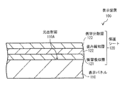
図1は、本開示の一実施の形態に係る表示装置100の断面構成の一例を表したものである。表示装置100は、光出射面110Aを有する表示パネル110と、表示パネル110の光出射面110Aに設けられた保護シート120とを備えている。表示パネル110は、光出射面110Aの直下に2次元配置された複数の表示画素を有しており、各表示画素から出射された光によって画像光Lを生成する。表示パネル110の外縁部分には、複数の表示画素を駆動するドライバが実装されている。表示装置100は、表示パネル110を制御するコントローラを備えており、コントローラからの制御信号に基づいて表示パネル110を制御する。
<1. Embodiment>
[Constitution]
FIG. 1 illustrates an example of a cross-sectional configuration of a
(表示パネル110)
表示パネル110は、コントローラからの制御信号に基づいて、画像光Lを生成し、生成した画像光Lを、光出射面110Aを介して外部に出射する。表示パネル110は、例えば、有機ELパネル、または、液晶パネルである。なお、表示パネル110は、有機ELパネルや液晶パネルに限定されるものではなく、他の方式の表示パネルであってもよい。
(Display panel 110)
The
図2は、表示パネル110の断面構成の一例を表したものである。図2に記載の表示パネル110は、トップエミッション型の有機ELパネルである。表示パネル110は、例えば、図2に示したように、素子形成基板111、TFT層112、有機層113および封止基板114を有している。素子形成基板111、TFT層112、有機層113および封止基板114は、光出射面110Aに向かってこの順に配置されている。例えば、封止基板114の表面が光出射面110Aとなっている。素子形成基板111は、TFT層112や有機層113を形成する際に用いられた基板であり、例えば、ガラス基板、または、プラスチック基板で構成されている。
FIG. 2 illustrates an example of a cross-sectional configuration of the
ガラス基板としては、例えば、高歪点ガラス、ソーダ石灰ガラス(Na2O・CaO・SiO2)、硼珪酸ガラス(Na2O・B2O2・SiO2)、フォルステライト(2MgO・SiO2)および鉛ガラス(Na2O・PbO・SiO2)などが挙げられる。プラスチック基板としては、例えば、ポリメチルメタクリレート(ポリメタクリル酸メチル,PMMA)、ポリビニルアルコール(PVA)、ポリビニルフェノール(PVP)、ポリエーテルスルホン(PES)、ポリイミド(PI)、ポリカーボネート(PC)、ポリエチレンテレフタレート(PET)あるいはトリアセチルセルロース(TAC)などの有機ポリマーによって構成された基板が挙げられる。なお、プラスチック基板は、可撓性を有するフィルム状あるいはシート状の基板であってもよい。 Examples of the glass substrate include high strain point glass, soda lime glass (Na 2 O · CaO · SiO 2 ), borosilicate glass (Na 2 O · B 2 O 2 · SiO 2 ), and forsterite (2MgO · SiO 2). ) And lead glass (Na 2 O · PbO · SiO 2 ). Examples of the plastic substrate include polymethyl methacrylate (polymethyl methacrylate, PMMA), polyvinyl alcohol (PVA), polyvinyl phenol (PVP), polyethersulfone (PES), polyimide (PI), polycarbonate (PC), and polyethylene terephthalate. Examples thereof include a substrate made of an organic polymer such as (PET) or triacetyl cellulose (TAC). The plastic substrate may be a flexible film or sheet substrate.
有機層113は、例えば、表示画素ごとに1つずつ設けられた複数の有機EL素子を含む層である。各有機EL素子から発せられる光によって画像光Lが形成される。TFT層112は、例えば、表示画素ごとに1つずつ設けられた複数の画素回路を含む層である。各画素回路は、対応する表示画素に含まれる有機EL素子に流れる電流を制御する。封止基板114は、有機層113内の複数の有機EL素子を封止するものであり、必要に応じて、カラーフィルターやブラックマトリクスなどを含んで構成されている。封止基板114は、素子形成基板111と同一の材料で構成された基板を含んでいてもよい。封止基板114が、偏光板で構成されていてもよい。封止基板114が、低リタデーションフィルムと、偏光板とを互いに重ね合わせたもので構成されていてもよい。表示パネル110において、封止基板114が省略されていてもよい。
For example, the
図3は、表示パネル110の断面構成の一例を表したものである。図3に記載の表示パネル110は、ボトムエミッション型の有機ELパネルである。表示パネル110は、例えば、図3に示したように、素子形成基板111、TFT層112、有機層113および封止基板114を有している。素子形成基板111、TFT層112、有機層113および封止基板114は、光出射面110A側からこの順に配置されている。例えば、素子形成基板111の表面が光出射面110Aとなっている。
FIG. 3 illustrates an example of a cross-sectional configuration of the
図2または図3の表示パネル110において、素子形成基板111および封止基板114は、フレキシブルなプラスチック基板で構成されていてもよい。この場合、表示パネル110は、フレキシブルな有機ELパネルとなる。
In the
図4は、表示パネル110の断面構成の一例を表したものである。図4に記載の表示パネル110は、液晶パネルである。表示パネル110は、例えば、図4に示したように、バックライト115、偏光板116、液晶層117および偏光板118を有している。バックライト115、偏光板116、液晶層117および偏光板118が、光出射面110Aに向かってこの順に配置されている。例えば、偏光板118の表面が光出射面110Aとなっている。バックライト115は、偏光板116、液晶層117および偏光板118からなる光変調部に対して、偏光板116側から面発光光を供給する。偏光板116および偏光板118の各透過軸は、液晶層117の駆動モード等に応じた設定となっており、例えば、クロスニコルの関係となるように設定されている。液晶層117は、印加電圧に応じて、液晶層117を透過する光の透過率を制御する。液晶層117は、例えば、VA(Vertical Alignment)モード、TN(Twisted Nematic)モード、ECB(Electrically controlled birefringence)モード、FFS(Fringe Field Switching)モード、またはIPS(In Plane Switching)モード等により表示駆動される液晶を含む。
FIG. 4 illustrates an example of a cross-sectional configuration of the
(保護シート120)
保護シート120は、表示パネル110の光出射面110Aを保護するものである。保護シート120は、さらに、画像光Lに対して光透過性を有するフレキシブルなシートで構成されている。保護シート120は、例えば、図1に示したように、衝撃吸収層121、歪み緩和層122および衝撃分散層123を有している。衝撃吸収層121、歪み緩和層122および衝撃分散層123は、表示パネル110の光出射面110A側からこの順に配置されている。衝撃吸収層121が、衝撃吸収層121、歪み緩和層122および衝撃分散層123の中で最も光出射面110A寄りに配置されている。衝撃分散層123が、衝撃吸収層121、歪み緩和層122および衝撃分散層123の中で最も光出射面110Aから離れて配置されている。歪み緩和層122は、衝撃吸収層121と衝撃分散層123との間に配置されている。
(Protective sheet 120)
The
(衝撃分散層123)
衝撃分散層123は、外部から加わった衝撃を一点に集中させないように分散させる機能と、引っ掻き等によって表面にキズが付くことを防止する機能とを持つ。衝撃分散層123は、鉛筆硬度3H以上の硬度を持った樹脂フィルムによって構成されている。衝撃分散層123の硬度の上限は、特に限定されない。衝撃分散層123は、例えば、鉛筆硬度10H以下の硬度を持った樹脂フィルムによって構成されている。樹脂フィルムの硬度を高めるためには、フィルム基材表面にハードコート材料を塗布または蒸着することが一般に行われる。しかし、フィルム基材の片面にハードコート処理した場合には、フィルム基材に反りが発生しやすく、貼合プロセスが困難になりやすい。また、フィルム基材の片面にハードコート処理されたもの(以下、「片面HC(Hard Coat)処理フィルム」と称する。)を貼合した場合には、貼合した樹脂フィルムが残留応力により割れたり、反ったりしてしまうことがある。そこで、衝撃分散層123は、ハードコート材料を固めてフィルム状にしたもの(以下、「HC(Hard Coat)フィルム」と称する。)、または、フィルム基材の両面にハードコート処理されたフィルム(以下、「両面HC処理フィルム」と称する。)によって構成されていることが好ましい。
(Shock dispersion layer 123)
The
HCフィルムおよび両面HC処理フィルムでは、反りの発生が少なく、所望の鉛筆硬度やヤング率、厚みを実現することができる。そのため、HCフィルムおよび両面HC処理フィルムは、衝撃分散層123として適している。
The HC film and the double-sided HC-treated film are less likely to warp, and can achieve a desired pencil hardness, Young's modulus, and thickness. Therefore, the HC film and the double-sided HC treatment film are suitable as the
衝撃分散層123において、曲げに強い材料が選択された場合には、落球試験の衝撃耐性が向上する。図5は、4種類のHCフィルム(片面HC処理フィルム、両面HC処理フィルム、HCフィルム)の曲げ破壊ひずみと落球試験の破壊高さの実験結果を表したものである。図5から、曲げ破壊ひずみの高いフィルムは、落球試験による破壊限界高さも高い傾向にあることがわかる。衝撃分散層123の割れを抑制する観点からは、衝撃分散層123は、曲げ破壊ひずみが4%以上のHCフィルム、または、曲げ破壊ひずみが4%以上の両面HC処理フィルムによって構成されていることが好ましい。
When a material resistant to bending is selected for the
(衝撃吸収層121)
衝撃吸収層121は、衝撃分散層123が衝撃を受けた際に、当該衝撃吸収層121が衝撃分散層123に生じた湾曲に応じた変形をすることにより、外部からの衝撃を吸収する機能(衝撃吸収機能)を持つ。衝撃吸収層121は、サブミリオーダ以上の厚さを有するゲル状の樹脂層である。衝撃吸収層121を構成するゲル状の樹脂層では、アスカーC硬度が30以上80以下となっていることが好ましい。アスカーC硬度が30よりも小さい場合、衝撃吸収層121が衝撃により潰れてしまい、衝撃を十分吸収できなくなる可能性がある。また、アスカーC硬度が80よりも大きい場合、衝撃が加わった際のゲルの変形が小さく、衝撃を十分吸収できなくなる可能性がある。本実施の形態では、衝撃分散層123が設けられているので、衝撃吸収層121の厚さは、衝撃分散層123が設けられていない場合に衝撃吸収層121として必要とされる厚さ(例えば、2mm程度)よりも薄くなっている。
(Shock absorbing layer 121)
The
衝撃吸収層121は、ゲル状接着層であってもよい。このとき、衝撃吸収層121は、保護シート120を光出射面110Aに直接もしくは間接的に貼合する機能(貼合機能)を有している。衝撃吸収層121がゲル状接着層である場合、衝撃吸収層121は、例えば、アクリル系のゲル状接着剤で構成されている。ゲル状接着剤としては、シリコーンゲルなども候補に挙げることが可能ではある。しかし、シリコーンゲルでは、油の染み出しが発生する可能性あり、ディスプレイの信頼性を低下させるおそれがある。
The
(歪み緩和層122)
歪み緩和層122は、荷重に対する衝撃分散層123の割れ耐性を高めるためのものである。衝撃分散層123に曲げ耐性の高い部材が使用された場合であっても、その下層に非常に柔らかい衝撃吸収層121があるときには、荷重によって衝撃分散層123が大きくたわみ、曲げ破壊ひずみを超えて割れてしまう可能性がある。そこで、本実施の形態では、荷重に対する衝撃分散層123の割れ耐性を高めるために、衝撃分散層123と衝撃吸収層121の間に歪み緩和層122が挿入されている。
(Strain relaxation layer 122)
The
歪み緩和層122は、衝撃分散層123よりも曲げ強度および引っ張り強度の高い樹脂フィルムによって構成されている。そのような樹脂フィルムとしては、例えば、PETフィルムが挙げられる。
The
図6は、歪み緩和層122が設けられている場合と、設けられていない場合とにおいて、保護シート120の表面からの荷重によって各層の歪みがどのように分布するかを応力シミュレーションで求めた結果を表したものである。図6から、歪み緩和層122が設けられていることにより、衝撃分散層123の歪みが緩和され、衝撃分散層123が割れにくくなっていることがわかる。
FIG. 6 shows the result of stress simulation of how the strain of each layer is distributed by the load from the surface of the
以下に、衝撃分散層123と歪み緩和層122との組み合わせの例を挙げる。
衝撃分散層123 歪み緩和層122
1. 有機/無機ハイブリッドHCフィルム PET
2. 有機/無機ハイブリッドHCフィルム TAC
3. 有機/無機ハイブリッドHCフィルム PI
4. PET基材HC処理フィルム PET
5. PET基材HC処理フィルム TAC
6. PET基材HC処理フィルム PI
7. TAC基材HC処理フィルム PET
8. TAC基材HC処理フィルム TAC
9. TAC基材HC処理フィルム PI
10.PC基材HC処理フィルム PET
11.PC基材HC処理フィルム TAC
12.PC基材HC処理フィルム PI
13.PMMA基材HC処理フィルム PET
14.PMMA基材HC処理フィルム TAC
15.PMMA基材HC処理フィルム PI
Examples of combinations of the
1. Organic / inorganic hybrid HC film PET
2. Organic / inorganic hybrid HC film TAC
3. Organic / inorganic hybrid HC film PI
4). PET substrate HC treatment film PET
5). PET substrate HC treatment film TAC
6). PET substrate HC treatment film PI
7). TAC substrate HC treatment film PET
8). TAC substrate HC treatment film TAC
9. TAC substrate HC treatment film PI
10. PC substrate HC treatment film PET
11. PC substrate HC treatment film TAC
12 PC substrate HC treatment film PI
13. PMMA base HC treatment film PET
14 PMMA base HC treatment film TAC
15. PMMA-based HC treatment film PI
HCフィルム:ハードコート材料を固めてフィルム状にしたもの
有機/無機ハイブリッド:有機材料と無機材料とが混ぜ合わされたハードコート材料
HC処理フィルム:フィルム基材にハードコート処理されたフィルム
PET基材:PETで形成されたフィルム基材
TAC基材:TACで形成されたフィルム基材
PC基材:PCで形成されたフィルム基材
PMMA基材:PMMAで形成されたフィルム基材
HC film: Hard coat material hardened into a film shape Organic / inorganic hybrid: Hard coat material in which organic material and inorganic material are mixed HC treated film: Film hard-coated on film base material PET base material: Film substrate formed of PET TAC substrate: Film substrate formed of TAC PC substrate: Film substrate formed of PC PMMA substrate: Film substrate formed of PMMA
上記の例では、保護シート120は、衝撃吸収層121、歪み緩和層122および衝撃分散層123を表示パネル110側からこの順に積層した構造となっている。しかし、保護シート120における積層構造の種類はこの限りではない。保護シート120は、例えば、図7に示したように、衝撃吸収層121、歪み緩和層122および衝撃分散層123を表示パネル110側からこの順に積層した積層体120Aを、複数、積層した構造となっていてもよい。また、保護シート120は、例えば、図8に示したように、複数の衝撃吸収層121、複数の歪み緩和層122および複数の衝撃分散層123を表示パネル110側からこの順に積層した構造となっていてもよい。この場合、衝撃吸収層121の積層数、歪み緩和層122の積層数および衝撃分散層123の積層数は、互いに同一であってもよいし、互いに異なっていてもよい。このように積層数を増やすことで衝撃耐性をさらに上げることができる。
In the above example, the
[効果]
次に、表示装置100における効果について説明する。
[effect]
Next, effects in the
外部からの衝撃によって、ディスプレイの表面に傷が付いたり、ディスプレイ内部が破壊され、機能が損なわれたりすることがある。特に、フレキシブルディスプレイには、薄い、軽い、柔軟といった特徴がある一方で、衝撃耐性が低いという欠点がある。従来では、ディスプレイの衝撃耐性を改善するために、ディスプレイの表面に強化ガラスが貼合されていた。しかし、重量や厚みが増してしまう欠点があった。また、フレキシブルディスプレイの表面に強化ガラスが貼合された場合には、薄い、軽い、柔軟といった特徴が損なわれてしまう。 The impact from the outside may damage the surface of the display, destroy the inside of the display, and impair the function. In particular, a flexible display has characteristics such as thinness, lightness, and flexibility, but has a drawback of low impact resistance. Conventionally, tempered glass has been bonded to the surface of the display in order to improve the impact resistance of the display. However, there is a drawback that the weight and thickness increase. In addition, when tempered glass is bonded to the surface of the flexible display, characteristics such as thinness, lightness, and flexibility are impaired.
一方、本実施の形態では、衝撃分散層123の下に設けられた衝撃吸収層121が、サブミリオーダ以上の厚さを有するゲル状の樹脂層によって構成されている。これにより、衝撃分散層123が衝撃を受けた際に、衝撃吸収層121が衝撃分散層123に生じた湾曲に応じた変形をするので、外部からの衝撃を吸収することができる。単に接着を目的として設けられた厚さの薄い接着層には、このような機能を持たせることはできない。
On the other hand, in the present embodiment, the
また、本実施の形態では、衝撃分散層123と衝撃吸収層121との間に、衝撃分散層123よりも曲げ強度および引っ張り強度の高い歪み緩和層122が設けられている。これにより、衝撃分散層123の下に非常に柔らかい衝撃吸収層121が設けられている場合であっても、衝撃分散層123が曲げ破壊ひずみを超えて割れてしまう可能性を低減することができる。従って、本実施の形態では、強化ガラスを使用しなくても、割れの発生を抑えつつ、外部からの衝撃を吸収することができる。
In this embodiment, a
また、本実施の形態において、衝撃吸収層121がゲル状接着層で構成されている場合には、保護シート120を直接または間接的に表示パネル110の光出射面110Aに貼り合わせることができる。これにより、既存の表示パネル110に対して、あと付けで保護シート120を設けることができる。その結果、既存の表示パネル110に対して保護シート120を設けることで、割れの発生を抑えつつ、外部からの衝撃を吸収することができる。
Further, in the present embodiment, when the
また、本実施の形態において、衝撃吸収層121がアクリル系のゲル状接着剤で構成されている場合には、シリコンゲルのような油の染み出しが起こらないので、ディスプレイの信頼性を低下させるおそれがない。
Further, in the present embodiment, when the
また、本実施の形態において、素子形成基板111および封止基板114がフレキシブルなプラスチック基板で構成されており、表示パネル110がフレキシブルな有機ELパネルとなっている場合には、表示パネル110および保護シート120を含む積層体全体がフレキシブルなディスプレイとなる。これにより、上記積層体を丸めて持ち運んだり、曲面の壁に貼りつけたりと、持ち運びや用途の自由度を高くすることができる。
In this embodiment, when the element formation substrate 111 and the sealing
<2.変形例>
以下に、表示装置100の変形例について説明する。なお、以下では、上記実施の形態の表示装置100と共通する構成要素に対しては、同一の符号が付与される。さらに、上記実施の形態の表示装置100と共通する構成要素についての説明は、適宜、省略されるものとする。
<2. Modification>
Below, the modification of the
[変形例A]
上記実施の形態において、衝撃吸収層121、歪み緩和層122および衝撃分散層123が、それぞれ、樹脂シートで構成されていてもよい。この場合、表示装置100は、例えば、図9に示したように、衝撃吸収層121と表示パネル110との間、歪み緩和層122と衝撃吸収層121との間、および衝撃分散層123と歪み緩和層122との間に、接着層126を備えていてもよい。
[Modification A]
In the above embodiment, each of the
[変形例B]
上記実施の形態において、保護シート120は、例えば、図10に示したように、光出射面110Aと衝撃吸収層121との間に、光学フィルム124、または、透明配線を含むタッチパネル125を有していてもよい。光学フィルム124としては、例えば、偏光板(例えば、円偏光板)や、防眩フィルム(AG(Anti Glare)フィルム)、反射防止フィルム(LR(Low Reflection)フィルムなどが挙げられる。タッチパネル125における透明配線は、例えば、ITO(Indium Tin Oxide;酸化インジウムスズ)などの光透過性の導電性材料によって構成されている。透明配線を含むタッチパネル125は非常に割れやすいので、衝撃吸収層121の下に配置されていることが好ましい。
[Modification B]
In the above embodiment, the
[変形例C]
上記実施の形態において、歪み緩和層122が、例えば、図11に示したように、偏光板などの光学フィルム127、または、Cuなどの金属配線を含むタッチパネル128によって構成されていてもよい。金属配線を含むタッチパネル128では、透明配線を含むタッチパネル125と比べて、柔軟性や衝撃耐性が高い。そのため、偏光板などの光学フィルム127、または、金属配線を含むタッチパネル128を、歪み緩和層122として設けることにより、保護シート120の厚さを薄くすることができ、また、製造コストを安価にすることができる。
[Modification C]
In the said embodiment, as shown in FIG. 11, the
[変形例D]
上記実施の形態において、素子形成基板111および封止基板114がフレキシブルなプラスチック基板で構成されており、表示パネル110がフレキシブルな有機ELパネルとなっている場合に、表示装置100は、例えば、図12に示したように、表示パネル110の背面に保護シート130を備えていてもよい。保護シート130は、表示パネル110の剛性を高め、表示パネル110に衝撃が加わった際の表示パネル110の局所的な撓みを低減する機能を有する。保護シート130は、ヤング率が高く、塑性変形しにくい材料によって構成されていることが好ましく、例えば、42Ni、SUS、Mg合金、Al等の金属材料によって構成されていることが好ましい。保護シート130が上述したような金属材料によって構成されている場合には、表示パネル110で生じた熱を保護シート130から放散させることもできる。なお、保護シート130が、保護シート120と同程度の剛性を有する樹脂シート(例えば、PET、PI、PC、PMMA等の樹脂シート)で構成されていてもよい。この場合にも、保護シート120と同様の効果が得られる。
[Modification D]
In the above embodiment, when the element formation substrate 111 and the sealing
[変形例E]
上記実施の形態において、素子形成基板111および封止基板114がフレキシブルなプラスチック基板で構成されており、表示パネル110がフレキシブルな有機ELパネルとなっている場合に、表示装置100は、例えば、図13に示したように、表示パネル110の背面に保護シート140を備えていてもよい。保護シート140は、例えば、図10に示したように、衝撃吸収層141、歪み緩和層142および衝撃分散層143を有している。衝撃吸収層141、歪み緩和層142および衝撃分散層143は、表示パネル110の背面側からこの順に配置されている。衝撃吸収層141が、衝撃吸収層141、歪み緩和層142および衝撃分散層143の中で最も表示パネル110の背面寄りに配置されている。衝撃分散層143が、衝撃吸収層141、歪み緩和層142および衝撃分散層143の中で最も表示パネル110の背面から離れて配置されている。歪み緩和層142は、衝撃吸収層141と衝撃分散層143との間に配置されている。衝撃吸収層141は、衝撃吸収層121の構成と同一の構成となっている。歪み緩和層142は、歪み緩和層122の構成と同一の構成となっている。衝撃分散層143は、衝撃分散層123の構成と同一の構成となっている。
[Modification E]
In the above embodiment, when the element formation substrate 111 and the sealing
本変形例では、表示パネル110の背面に設けられた保護シート140が保護シート120と共通の構成となっている。これにより、保護シート120が表示パネル110に与える応力と、保護シート140が表示パネル110に与える応力とが相殺し合うので、保護シート120に起因する表示パネル110の反りや撓みを防止することができる。
In this modification, the
<3.適用例>
以下、上記実施の形態およびその変形例(以下、「上記実施の形態等」と称する。)で説明した表示装置100の適用例について説明する。上記実施の形態等の表示装置100は、テレビジョン装置、デジタルカメラ、ノート型パーソナルコンピュータ、シート状のパーソナルコンピュータ、携帯電話等の携帯端末装置あるいはビデオカメラなど、外部から入力された映像信号あるいは内部で生成した映像信号を、画像あるいは映像として表示するあらゆる分野の電子機器の表示装置に適用することが可能である。
<3. Application example>
Hereinafter, application examples of the
図14は、本適用例に係る電子機器200の外観を斜視的に表したものである。電子機器200は、例えば、筐体210の主面に表示面を備えたシート状のパーソナルコンピュータである。電子機器200は、電子機器200の表示面に、上記実施の形態等の表示装置100を備えている。表示装置100は、保護シート120が外側を向くように配置されている。本適用例では、表示装置100に対して保護シート120が設けられているので、軽量かつ、割れの発生し難い電子機器200を実現することができる。
FIG. 14 is a perspective view of the appearance of the
また、本適用例において、表示装置100に対して保護シート140も設けられている場合には、反りや撓みの少ない電子機器200を実現することができる。
In this application example, in the case where the
以上、実施の形態、変形例および適用例を挙げて本開示を説明したが、本開示は実施の形態等に限定されるものではなく、種々変形が可能である。なお、本明細書中に記載された効果は、あくまで例示である。本開示の効果は、本明細書中に記載された効果に限定されるものではない。本開示が、本明細書中に記載された効果以外の効果を持っていてもよい。 Although the present disclosure has been described with the embodiment, the modification, and the application example, the present disclosure is not limited to the embodiment and the like, and various modifications can be made. In addition, the effect described in this specification is an illustration to the last. The effects of the present disclosure are not limited to the effects described in this specification. The present disclosure may have effects other than those described in this specification.
また、例えば、本開示は以下のような構成を取ることができる。
(1)
光出射面を有する表示パネルと、
前記光出射面に設けられた第1保護シートと
を備え、
前記第1保護シートは、
鉛筆硬度3H以上の第1衝撃分散層と、
前記第1衝撃分散層よりも曲げ強度および引っ張り強度の高い第1歪み緩和層と、
サブミリオーダ以上の厚さを有するゲル状の第1衝撃吸収層と
を有し、
前記第1衝撃吸収層、前記第1歪み緩和層および前記第1衝撃分散層は、前記光出射面からこの順に並んで配置されている
表示装置。
(2)
前記第1衝撃吸収層は、前記第1保護シートを前記光出射面に直接もしくは間接的に貼合する、アスカーC硬度が30以上80以下のゲル状接着層である
(1)に記載の表示装置。
(3)
前記第1衝撃吸収層は、アクリル系のゲル状接着剤で構成されている
(2)に記載の表示装置。
(4)
前記表示パネルは、フレキシブルなパネルである
(1)ないし(3)のいずれか1つに記載の表示装置。
(5)
前記表示パネルは、有機ELパネルである
(1)ないし(4)のいずれか1つに記載の表示装置。
(6)
前記第1保護シートは、前記光出射面と前記第1衝撃吸収層との間に、偏光板、または、透明配線を含むタッチパネルを有する
(1)ないし(5)のいずれか1つに記載の表示装置。
(7)
前記第1歪み緩和層は、偏光板、または、金属配線を含むタッチパネルである
(1)ないし(4)のいずれか1つに記載の表示装置。
(8)
前記表示パネルの背面に設けられた第2保護シートをさらに備え、
前記第2保護シートは、
鉛筆硬度3H以上の第2衝撃分散層と、
前記第2衝撃分散層よりも曲げ強度および引っ張り強度の高い第2歪み緩和層と、
サブミリオーダ以上の厚さを有するゲル状の第2衝撃吸収層と
を有し、
前記第2衝撃吸収層、前記第2歪み緩和層および前記第2衝撃分散層は、前記背面からこの順に並んで配置されている
(1)ないし(7)のいずれか1つに記載の表示装置。
(9)
表示装置を備え、
前記表示装置は、
光出射面を有する表示パネルと、
前記光出射面に設けられた第1保護シートと
を有し、
前記第1保護シートは、
鉛筆硬度3H以上の第1衝撃分散層と、
前記第1衝撃分散層よりも曲げ強度および引っ張り強度の高い第1歪み緩和層と、
サブミリオーダ以上の厚さを有するゲル状の第1衝撃吸収層と
を有し、
前記第1衝撃吸収層、前記第1歪み緩和層および前記第1衝撃分散層は、前記光出射面からこの順に並んで配置されている
電子機器。
(10)
表示パネルの光出射面を保護する保護シートであって、
鉛筆硬度3H以上の第1衝撃分散層と、
前記第1衝撃分散層よりも曲げ強度および引っ張り強度の高い第1歪み緩和層と、
サブミリオーダ以上の厚さを有するゲル状の第1衝撃吸収層と
を有し、
前記第1衝撃吸収層、前記第1歪み緩和層および前記第1衝撃分散層は、この順に並んで配置されている
保護シート。
For example, this indication can take the following composition.
(1)
A display panel having a light exit surface;
A first protective sheet provided on the light exit surface,
The first protective sheet is
A first impact dispersion layer having a pencil hardness of 3H or more;
A first strain relaxation layer having higher bending strength and tensile strength than the first impact dispersion layer;
A gel-like first shock absorbing layer having a thickness of at least sub-milliorder,
The display device, wherein the first shock absorbing layer, the first strain relaxation layer, and the first shock dispersion layer are arranged in this order from the light emitting surface.
(2)
The display according to (1), wherein the first shock absorbing layer is a gel-like adhesive layer having an Asker C hardness of 30 to 80, which directly or indirectly bonds the first protective sheet to the light emitting surface. apparatus.
(3)
The display device according to (2), wherein the first shock absorbing layer is made of an acrylic gel adhesive.
(4)
The display device according to any one of (1) to (3), wherein the display panel is a flexible panel.
(5)
The display device according to any one of (1) to (4), wherein the display panel is an organic EL panel.
(6)
The first protective sheet has a touch panel including a polarizing plate or a transparent wiring between the light emitting surface and the first shock absorbing layer. (1) to (5) Display device.
(7)
The display device according to any one of (1) to (4), wherein the first strain relaxation layer is a polarizing plate or a touch panel including metal wiring.
(8)
A second protective sheet provided on the back surface of the display panel;
The second protective sheet is
A second impact dispersion layer having a pencil hardness of 3H or more;
A second strain relaxation layer having higher bending strength and tensile strength than the second impact dispersion layer;
A gel-like second shock absorbing layer having a thickness of at least sub-milliorder,
The display device according to any one of (1) to (7), wherein the second shock absorption layer, the second strain relaxation layer, and the second shock dispersion layer are arranged in this order from the back surface. .
(9)
A display device,
The display device
A display panel having a light exit surface;
A first protective sheet provided on the light exit surface,
The first protective sheet is
A first impact dispersion layer having a pencil hardness of 3H or more;
A first strain relaxation layer having higher bending strength and tensile strength than the first impact dispersion layer;
A gel-like first shock absorbing layer having a thickness of at least sub-milliorder,
The electronic device in which the first shock absorption layer, the first strain relaxation layer, and the first shock dispersion layer are arranged in this order from the light emitting surface.
(10)
A protective sheet for protecting the light emission surface of the display panel,
A first impact dispersion layer having a pencil hardness of 3H or more;
A first strain relaxation layer having higher bending strength and tensile strength than the first impact dispersion layer;
A gel-like first shock absorbing layer having a thickness of at least sub-milliorder,
The first impact absorbing layer, the first strain relaxation layer, and the first impact dispersion layer are arranged in this order.
100…表示装置、110…表示パネル、110A…光出射面、111…素子形成基板、112…TFT層、113…有機層、114…封止基板、115…バックライト、116…偏光板、117…液晶層、118…偏光板、120…保護シート、120A…積層体、121…衝撃吸収層、122…歪み緩和層、123…衝撃分散層、124…光学フィルム、125…タッチパネル、126…接着層、127…光学フィルム、128…タッチパネル、130…保護シート、140…保護シート、141…衝撃吸収層、142…歪み緩和層、143…衝撃分散層、200…電子機器、210…筐体、L…画像光。
DESCRIPTION OF
Claims (7)
前記光出射面に設けられた第1保護シートと、
前記表示パネルの背面に設けられた第2保護シートと
を備え、
前記第1保護シートは、
鉛筆硬度3H以上の第1衝撃分散層と、
前記第1衝撃分散層よりも曲げ強度および引っ張り強度の高い第1歪み緩和層と、
サブミリオーダ以上の厚さを有するゲル状の第1衝撃吸収層と
を有し、
前記第1衝撃吸収層、前記第1歪み緩和層および前記第1衝撃分散層は、前記光出射面からこの順に並んで配置されており、
前記第2保護シートは、金属材料によって構成されている
表示装置。 A flexible display panel having a light exit surface;
A first protective sheet provided on the light exit surface;
A second protective sheet provided on the back surface of the display panel,
The first protective sheet is
A first impact dispersion layer having a pencil hardness of 3H or more;
A first strain relaxation layer having higher bending strength and tensile strength than the first impact dispersion layer;
A gel-like first shock absorbing layer having a thickness of at least sub-milliorder,
The first shock absorbing layer, the first strain relaxation layer, and the first shock dispersion layer are arranged in this order from the light emitting surface,
The second protective sheet is made of a metal material. Display device.
請求項1に記載の表示装置。 The display according to claim 1 , wherein the first shock absorbing layer is a gel-like adhesive layer having an Asker C hardness of 30 or more and 80 or less, which directly or indirectly bonds the first protective sheet to the light emitting surface. apparatus.
請求項2に記載の表示装置。 The display device according to claim 2 , wherein the first shock absorbing layer is made of an acrylic gel adhesive.
請求項1ないし請求項3のいずれか一項に記載の表示装置。 The display device according to any one of claims 1 to 3 , wherein the display panel is an organic EL panel.
請求項4に記載の表示装置。 The display device according to claim 4 , wherein the first protective sheet includes a touch panel including a polarizing plate or a transparent wiring between the light emitting surface and the first shock absorbing layer.
請求項4に記載の表示装置。 The display device according to claim 4 , wherein the first strain relaxation layer is a polarizing plate or a touch panel including metal wiring.
前記表示装置は、
光出射面を有するフレキシブルな表示パネルと、
前記光出射面に設けられた第1保護シートと、
前記表示パネルの背面に設けられた第2保護シートと
を有し、
前記第1保護シートは、
鉛筆硬度3H以上の第1衝撃分散層と、
前記第1衝撃分散層よりも曲げ強度および引っ張り強度の高い第1歪み緩和層と、
サブミリオーダ以上の厚さを有するゲル状の第1衝撃吸収層と
を有し、
前記第1衝撃吸収層、前記第1歪み緩和層および前記第1衝撃分散層は、前記光出射面からこの順に並んで配置されており、
前記第2保護シートは、金属材料によって構成されている
電子機器。 A display device,
The display device
A flexible display panel having a light exit surface;
A first protective sheet provided on the light exit surface;
A second protective sheet provided on the back surface of the display panel,
The first protective sheet is
A first impact dispersion layer having a pencil hardness of 3H or more;
A first strain relaxation layer having higher bending strength and tensile strength than the first impact dispersion layer;
A gel-like first shock absorbing layer having a thickness of at least sub-milliorder,
The first shock absorbing layer, the first strain relaxation layer, and the first shock dispersion layer are arranged in this order from the light emitting surface,
The second protective sheet is an electronic device made of a metal material.
Priority Applications (3)
| Application Number | Priority Date | Filing Date | Title |
|---|---|---|---|
| JP2016044217A JP6603154B2 (en) | 2016-03-08 | 2016-03-08 | Display device and electronic device |
| US15/440,825 US10109816B2 (en) | 2016-03-08 | 2017-02-23 | Protective sheet, display unit, and electronic apparatus |
| JP2019186927A JP6925047B2 (en) | 2016-03-08 | 2019-10-10 | Display devices and electronic devices |
Applications Claiming Priority (1)
| Application Number | Priority Date | Filing Date | Title |
|---|---|---|---|
| JP2016044217A JP6603154B2 (en) | 2016-03-08 | 2016-03-08 | Display device and electronic device |
Related Child Applications (1)
| Application Number | Title | Priority Date | Filing Date |
|---|---|---|---|
| JP2019186927A Division JP6925047B2 (en) | 2016-03-08 | 2019-10-10 | Display devices and electronic devices |
Publications (3)
| Publication Number | Publication Date |
|---|---|
| JP2017161621A JP2017161621A (en) | 2017-09-14 |
| JP2017161621A5 JP2017161621A5 (en) | 2018-07-19 |
| JP6603154B2 true JP6603154B2 (en) | 2019-11-06 |
Family
ID=59787221
Family Applications (1)
| Application Number | Title | Priority Date | Filing Date |
|---|---|---|---|
| JP2016044217A Active JP6603154B2 (en) | 2016-03-08 | 2016-03-08 | Display device and electronic device |
Country Status (2)
| Country | Link |
|---|---|
| US (1) | US10109816B2 (en) |
| JP (1) | JP6603154B2 (en) |
Families Citing this family (11)
| Publication number | Priority date | Publication date | Assignee | Title |
|---|---|---|---|---|
| US10632711B2 (en) * | 2016-11-16 | 2020-04-28 | Samsung Display Co., Ltd. | Window for flexible display device and flexible display device having the same |
| KR102373443B1 (en) * | 2017-09-14 | 2022-03-14 | 삼성디스플레이 주식회사 | Display device |
| JP6556812B2 (en) * | 2017-11-28 | 2019-08-07 | Nissha株式会社 | Film type touch sensor with hard coat and flexible device using the same |
| TWI661344B (en) * | 2018-04-13 | 2019-06-01 | 友達光電股份有限公司 | Display device |
| JP6817257B2 (en) | 2018-07-31 | 2021-01-20 | 株式会社Joled | Protective sheets, display devices and electronic devices |
| KR102484586B1 (en) * | 2018-11-07 | 2023-01-03 | 엘지디스플레이 주식회사 | Foldable display device |
| US20220137266A1 (en) * | 2019-03-01 | 2022-05-05 | Dai Nippon Printing Co., Ltd. | Resin layer, optical film, and image display device |
| TW202043027A (en) * | 2019-03-21 | 2020-12-01 | 日商半導體能源研究所股份有限公司 | Display device and electronic device |
| EP3785897B1 (en) | 2019-08-29 | 2021-12-29 | SHPP Global Technologies B.V. | Transparent, flexible, impact resistant, multilayer film comprising polycarbonate copolymers |
| CN111816077B (en) | 2020-07-13 | 2022-04-26 | 武汉华星光电半导体显示技术有限公司 | Foldable display module |
| EP4235279A4 (en) * | 2020-11-27 | 2023-10-18 | Huawei Technologies Co., Ltd. | Screen cover, display apparatus, and electronic device |
Family Cites Families (15)
| Publication number | Priority date | Publication date | Assignee | Title |
|---|---|---|---|---|
| JP2000326447A (en) * | 1999-05-21 | 2000-11-28 | Dainippon Printing Co Ltd | Hard coat film |
| JP2002023649A (en) * | 2000-03-15 | 2002-01-23 | Nitto Denko Corp | Transparent impact relaxation laminated body and display device using the same |
| JP3999979B2 (en) * | 2002-02-25 | 2007-10-31 | 松下電器産業株式会社 | Impact-resistant film for flat display panel and flat display panel |
| TWI370272B (en) * | 2007-11-27 | 2012-08-11 | Ind Tech Res Inst | Polarizing plates and liquid crystal displays comprising the same |
| JP2009037119A (en) * | 2007-08-03 | 2009-02-19 | Seiko Epson Corp | Electrophoretic display device and electronic paper |
| JP5527790B2 (en) * | 2009-03-05 | 2014-06-25 | 日東電工株式会社 | Laminated optical film, liquid crystal panel, and liquid crystal display device |
| JP5530743B2 (en) * | 2009-04-14 | 2014-06-25 | リンテック株式会社 | Convex / concave following laminated member and display device with touch panel using the same |
| JP2011180252A (en) * | 2010-02-26 | 2011-09-15 | Sumitomo Chemical Co Ltd | Set of polarizing plate, and liquid crystal panel and liquid crystal display device using the same |
| US20130222317A1 (en) * | 2010-10-08 | 2013-08-29 | Sharp Kabushiki Kaisha | Display device, and process for manufacturing display device |
| KR101910111B1 (en) * | 2012-08-28 | 2018-10-22 | 삼성디스플레이 주식회사 | Foldable display device |
| US20140162009A1 (en) * | 2012-12-12 | 2014-06-12 | She Hwa P&C Co., Ltd | Shock absorption film and method of making the same |
| JP2015105993A (en) * | 2013-11-29 | 2015-06-08 | ルミネセンス株式会社 | Protective sheet for liquid crystal screen |
| JP6344951B2 (en) * | 2014-03-31 | 2018-06-20 | デクセリアルズ株式会社 | Thermally conductive sheet and method for producing thermally conductive sheet |
| JP2016002764A (en) * | 2014-06-19 | 2016-01-12 | 日本合成化学工業株式会社 | Laminate, use thereof, and production method thereof |
| JP6122812B2 (en) * | 2014-06-30 | 2017-04-26 | 富士フイルム株式会社 | Polarizing plate and image display device |
-
2016
- 2016-03-08 JP JP2016044217A patent/JP6603154B2/en active Active
-
2017
- 2017-02-23 US US15/440,825 patent/US10109816B2/en active Active
Also Published As
| Publication number | Publication date |
|---|---|
| US20170263889A1 (en) | 2017-09-14 |
| JP2017161621A (en) | 2017-09-14 |
| US10109816B2 (en) | 2018-10-23 |
Similar Documents
| Publication | Publication Date | Title |
|---|---|---|
| JP6603154B2 (en) | Display device and electronic device | |
| JP6817257B2 (en) | Protective sheets, display devices and electronic devices | |
| KR102563743B1 (en) | Protecting cover and display device comprising thereof | |
| JP5315064B2 (en) | Display device | |
| JP5433465B2 (en) | Display device | |
| US9442316B2 (en) | Display device comprising a light-transmitting cover having a lens portion | |
| KR102338473B1 (en) | Window cover and display apparatus having the same and method of manufacturing display apparatus | |
| KR101020924B1 (en) | Liquid crystal display device | |
| US20180081088A1 (en) | Display device protecting cover and display device comprising thereof | |
| WO2010140393A1 (en) | Liquid crystal display device | |
| WO2008047785A1 (en) | Display device | |
| KR20170050653A (en) | Flexible Display and Method for Manufacturing the Same | |
| JP2012133428A (en) | Display device | |
| JP2006071972A (en) | Display device | |
| KR102214353B1 (en) | Display Device | |
| JP2007108553A (en) | Electro-optic device and electronic equipment | |
| CN113192419B (en) | Display module and display device | |
| JP2015099285A (en) | Display device | |
| KR20140099527A (en) | Image display device | |
| US20170115446A1 (en) | Lighting device and display device | |
| KR20190053691A (en) | Display device | |
| JP3980405B2 (en) | Image display device | |
| JP2015184397A (en) | display device | |
| JP6925047B2 (en) | Display devices and electronic devices | |
| CN111462624B (en) | Protective member, display device, and method for manufacturing protective member |
Legal Events
| Date | Code | Title | Description |
|---|---|---|---|
| A711 | Notification of change in applicant |
Free format text: JAPANESE INTERMEDIATE CODE: A711 Effective date: 20170324 |
|
| A521 | Request for written amendment filed |
Free format text: JAPANESE INTERMEDIATE CODE: A821 Effective date: 20170324 |
|
| A521 | Request for written amendment filed |
Free format text: JAPANESE INTERMEDIATE CODE: A523 Effective date: 20180606 |
|
| A621 | Written request for application examination |
Free format text: JAPANESE INTERMEDIATE CODE: A621 Effective date: 20180606 |
|
| A977 | Report on retrieval |
Free format text: JAPANESE INTERMEDIATE CODE: A971007 Effective date: 20190225 |
|
| A131 | Notification of reasons for refusal |
Free format text: JAPANESE INTERMEDIATE CODE: A131 Effective date: 20190312 |
|
| A521 | Request for written amendment filed |
Free format text: JAPANESE INTERMEDIATE CODE: A523 Effective date: 20190409 |
|
| A131 | Notification of reasons for refusal |
Free format text: JAPANESE INTERMEDIATE CODE: A131 Effective date: 20190813 |
|
| A521 | Request for written amendment filed |
Free format text: JAPANESE INTERMEDIATE CODE: A523 Effective date: 20190826 |
|
| TRDD | Decision of grant or rejection written | ||
| A01 | Written decision to grant a patent or to grant a registration (utility model) |
Free format text: JAPANESE INTERMEDIATE CODE: A01 Effective date: 20190910 |
|
| A61 | First payment of annual fees (during grant procedure) |
Free format text: JAPANESE INTERMEDIATE CODE: A61 Effective date: 20191010 |
|
| R151 | Written notification of patent or utility model registration |
Ref document number: 6603154 Country of ref document: JP Free format text: JAPANESE INTERMEDIATE CODE: R151 |
|
| R250 | Receipt of annual fees |
Free format text: JAPANESE INTERMEDIATE CODE: R250 |
|
| S303 | Written request for registration of pledge or change of pledge |
Free format text: JAPANESE INTERMEDIATE CODE: R316303 |
|
| R350 | Written notification of registration of transfer |
Free format text: JAPANESE INTERMEDIATE CODE: R350 |
|
| S803 | Written request for registration of cancellation of provisional registration |
Free format text: JAPANESE INTERMEDIATE CODE: R316803 |
|
| R350 | Written notification of registration of transfer |
Free format text: JAPANESE INTERMEDIATE CODE: R350 |
|
| R250 | Receipt of annual fees |
Free format text: JAPANESE INTERMEDIATE CODE: R250 |