US10620649B2 - Current regulating circuit and method - Google Patents
Current regulating circuit and method Download PDFInfo
- Publication number
- US10620649B2 US10620649B2 US16/441,197 US201916441197A US10620649B2 US 10620649 B2 US10620649 B2 US 10620649B2 US 201916441197 A US201916441197 A US 201916441197A US 10620649 B2 US10620649 B2 US 10620649B2
- Authority
- US
- United States
- Prior art keywords
- level
- node
- current regulating
- nmos
- pmos
- Prior art date
- Legal status (The legal status is an assumption and is not a legal conclusion. Google has not performed a legal analysis and makes no representation as to the accuracy of the status listed.)
- Active
Links
- 230000001105 regulatory effect Effects 0.000 title claims abstract description 55
- 238000000034 method Methods 0.000 title claims description 16
- 239000003990 capacitor Substances 0.000 claims abstract description 16
- 230000003247 decreasing effect Effects 0.000 claims description 4
- 238000010586 diagram Methods 0.000 description 10
- 238000005516 engineering process Methods 0.000 description 6
- 230000004044 response Effects 0.000 description 6
- 230000004075 alteration Effects 0.000 description 1
- 238000010168 coupling process Methods 0.000 description 1
- 238000005859 coupling reaction Methods 0.000 description 1
- 238000012986 modification Methods 0.000 description 1
- 230000004048 modification Effects 0.000 description 1
- 230000008569 process Effects 0.000 description 1
Images


Classifications
-
- G—PHYSICS
- G05—CONTROLLING; REGULATING
- G05F—SYSTEMS FOR REGULATING ELECTRIC OR MAGNETIC VARIABLES
- G05F1/00—Automatic systems in which deviations of an electric quantity from one or more predetermined values are detected at the output of the system and fed back to a device within the system to restore the detected quantity to its predetermined value or values, i.e. retroactive systems
- G05F1/10—Regulating voltage or current
- G05F1/46—Regulating voltage or current wherein the variable actually regulated by the final control device is DC
- G05F1/56—Regulating voltage or current wherein the variable actually regulated by the final control device is DC using semiconductor devices in series with the load as final control devices
-
- H—ELECTRICITY
- H02—GENERATION; CONVERSION OR DISTRIBUTION OF ELECTRIC POWER
- H02M—APPARATUS FOR CONVERSION BETWEEN AC AND AC, BETWEEN AC AND DC, OR BETWEEN DC AND DC, AND FOR USE WITH MAINS OR SIMILAR POWER SUPPLY SYSTEMS; CONVERSION OF DC OR AC INPUT POWER INTO SURGE OUTPUT POWER; CONTROL OR REGULATION THEREOF
- H02M1/00—Details of apparatus for conversion
- H02M1/0003—Details of control, feedback or regulation circuits
- H02M1/0032—Control circuits allowing low power mode operation, e.g. in standby mode
- H02M1/0035—Control circuits allowing low power mode operation, e.g. in standby mode using burst mode control
-
- H02M2001/0032—
-
- H02M2001/0035—
-
- Y—GENERAL TAGGING OF NEW TECHNOLOGICAL DEVELOPMENTS; GENERAL TAGGING OF CROSS-SECTIONAL TECHNOLOGIES SPANNING OVER SEVERAL SECTIONS OF THE IPC; TECHNICAL SUBJECTS COVERED BY FORMER USPC CROSS-REFERENCE ART COLLECTIONS [XRACs] AND DIGESTS
- Y02—TECHNOLOGIES OR APPLICATIONS FOR MITIGATION OR ADAPTATION AGAINST CLIMATE CHANGE
- Y02B—CLIMATE CHANGE MITIGATION TECHNOLOGIES RELATED TO BUILDINGS, e.g. HOUSING, HOUSE APPLIANCES OR RELATED END-USER APPLICATIONS
- Y02B70/00—Technologies for an efficient end-user side electric power management and consumption
- Y02B70/10—Technologies improving the efficiency by using switched-mode power supplies [SMPS], i.e. efficient power electronics conversion e.g. power factor correction or reduction of losses in power supplies or efficient standby modes
Definitions
- the invention generally relates to current regulating technology, and more particularly, to current regulating technology for increasing the response speed of a low dropout regulator (LDO) for switching from a standby mode to an active mode by a current regulator.
- LDO low dropout regulator
- the low dropout regulator may have its corresponding active mode and standby mode (power-saving mode).
- FIG. 1 is a schematic diagram of the voltage levels of the control signal Vint_en and the reference node Node_i-ref according to the prior art. As shown in FIG. 1 , when the control signal Vint_en is changed from a low voltage level to a high voltage level (i.e. the low dropout regulator is switched from the standby mode to the active mode), the voltage level of the reference node Node_i-ref of the low dropout regulator is changed from a low voltage level to a target voltage level.
- the invention provides a current regulating technology to overcome the problems described above.
- the current regulating technology is more particularly related to the current regulating circuit and method for increasing the response speed of a low dropout regulator for switching from a standby mode to an active mode by a current regulator.
- An embodiment of the invention provides a current regulating circuit.
- the current regulating circuit comprises a first inverter, a second inverter, a PMOS, an NMOS and a capacitor.
- the first inverter receives a control signal.
- the second inverter receives the control signal.
- a first gate of the PMOS is coupled to the first inverter.
- the NMOS is coupled to the PMOS and a second gate of the NMOS is coupled to the second inverter.
- the capacitor is coupled to the PMOS and the NMOS at a node, and is coupled to a low dropout regulator at a reference node.
- An embodiment of the invention provides a current regulating method.
- the current regulating method is applied to a current regulating circuit.
- the current regulating method comprises the steps of when a control signal is changed from a first level to a second level, enabling a PMOS of the current regulating circuit and disabling an NMOS of the current regulating circuit, wherein the PMOS and the NMOS are coupled to a node; and pulling the voltage level of the node to a high level to increase the speed of pulling the voltage level of a reference node to a target voltage level, wherein the current regulating circuit and a low dropout regulator are coupled to the reference node.
- FIG. 1 is a schematic diagram of the voltage levels of the control signal Vint_en and the reference node Node_i-ref according to a prior art
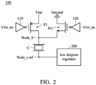
- FIG. 2 is a circuit diagram of a current regulating circuit 100 according to an embodiment of the invention.
- FIG. 3 is a circuit diagram of a low dropout regulator 200 according to an embodiment of the invention.
- FIG. 4 is a schematic diagram of the voltage levels of the control signal Vint_en, the node Node_ 0 and the reference node Node_i-ref according to an embodiment of the invention.
- FIG. 5 is a flow chart 500 illustrating the current regulating method according to an embodiment of the invention.
- FIG. 2 is a circuit diagram of a current regulating circuit 100 according to an embodiment of the invention.
- the current regulating circuit 100 may comprise a first inverter 110 , a second inverter 120 , a first PMOS P 1 , a first NMOS N 1 and a capacitor C.
- FIG. 2 presents a simplified circuit diagram in which only the elements relevant to the invention are shown. However, the invention should not be limited to what is shown in FIG. 2 .
- the current regulating circuit 100 may comprise other elements.
- the current regulating circuit 100 may be coupled to a low dropout (linear) regulator (LDO) 200 .
- LDO low dropout
- the capacitor C may comprise a plurality of capacitors. According different requirements of the capacitance value, the capacitors with different sizes may be configured in the capacitor C.
- the first inverter 110 is coupled to the first gate of the first PMOS P 1 , and the first inverter 110 may receive the control signal Vint_en from an external control circuit (not shown in figures).
- the second inverter 120 is coupled to the second gate of the first NMOS N 1 , and the second inverter 120 may also receive the control signal Vint_en from the external control circuit (not shown in figures).
- the first drain of the first PMOS P 1 is coupled to the capacitor C at the node Node_ 0
- the first source of the first PMOS P 1 may receive an input voltage Vint
- the second source of the first NMOS N 1 is coupled to the capacitor C at the node Node_ 0
- the second source of the first NMOS N 1 is coupled to a ground Ground.
- the capacitor C of the current regulating circuit 100 may be coupled to the low dropout regulator 200 at the reference node Node_i-ref.
- FIG. 3 is a circuit diagram of a low dropout regulator 200 according to an embodiment of the invention.
- the low dropout regulator 200 comprises an amplifier 210 , a second PMOS P 2 , a second NMOS N 2 , a third NMOS N 3 , a fourth NMOS N 4 , a fifth NMOS N 5 and a third inverter 220 .
- FIG. 3 presents a simplified circuit diagram in which only the elements relevant to the invention are shown. However, the invention should not be limited to what is shown in FIG. 3 .
- the low dropout regulator 200 may comprise other elements.
- the nodes in the same line with the reference node Node_i-ref can be regarded as reference node Node_i-ref.
- the external control circuit may also transmit the control signal Vint_en to the low dropout regulator 200 to control the low dropout regulator 200 to operate in a standby mode or an active mode.
- the control signal Vint_en when the control signal Vint_en is in a first level (e.g. a low level), the low dropout regulator 200 may operate in the standby mode, and when the control signal Vint_en is in a second level (e.g. a high level), the low dropout regulator 200 may operate in the active mode.
- a first level e.g. a low level
- a second level e.g. a high level
- the first path (i.e. the third NMOS N 3 and the fourth NMOS N 4 ) of the low dropout regulator 200 and the second path (i.e. the fifth NMOS N 5 ) of the low dropout regulator 200 will be enabled to put the voltage level of the reference node Node_i-ref at a low level.
- the first path (i.e. the third NMOS N 3 and the fourth NMOS N 4 ) of the low dropout regulator 200 will be disabled and the second path (i.e. the fifth NMOS N 5 ) of the low dropout regulator 200 will be enabled to put the voltage level of the reference node Node_i-ref be at a high level.
- the first PMOS P 1 when the control signal Vint_en received by the first inverter 110 and the second inverter 120 is first level (e.g. low level), the first PMOS P 1 will be disabled, the first NMOS N 1 will be enabled, and the voltage level of the node Node_ 0 will be in a low level. Because the first PMOS P 1 is disabled and the first NMOS N 1 is enabled, the current regulating circuit 100 is not enabled when the control signal Vint_en is first level (e.g. low level), i.e. the current regulating circuit 100 does not regulate the voltage level of the reference node Node_i-ref.
- the first PMOS P 1 when the control signal Vint_en received by the first inverter 110 and the second inverter 120 is second level (e.g. high level), the first PMOS P 1 will be enabled, the first NMOS N 1 will be disabled, and the voltage level of the node Node_ 0 will be in a high level. Because the first PMOS P 1 is enabled and the first NMOS N 1 is disabled, the current regulating circuit 100 will be enabled when the control signal Vint_en is second level (e.g. high level) in order to regulate the voltage level of the reference node Node_i-ref (i.e. increase the speed of pulling the voltage level of the reference node Node_i-ref to a target voltage level).
- the control signal Vint_en is second level (e.g. high level) in order to regulate the voltage level of the reference node Node Node_i-ref (i.e. increase the speed of pulling the voltage level of the reference node Node_i-ref to a target voltage level).
- the first PMOS P 1 is enabled, the first NMOS N 1 is disabled, and the voltage level of the node Node_ 0 is changed from the low level to the high level.
- the capacitor C is utilized to process the capacitive-coupling for the voltage level of the reference node Node_i-ref to increase the speed of pulling the voltage level of the reference node Node_i-ref to a target voltage level.
- control signal Vint_en when the control signal Vint_en is changed from the second level (high level) to the first level (low level), the first PMOS P 1 is disabled, the first NMOS N 1 is enabled, and the voltage level of the node Node_ 0 is changed from the high level to the low level.
- the size of the first PMOS P 1 is larger than the size of the first NMOS N 1 to allow the voltage level of the node Node_ 0 to be changed from the low level to high level instantaneously, when the control signal Vint_en is changed from the first level (low level) to the second level (high level), and allow the voltage level of the node Node_ 0 to be changed gradually from the high level to low level, when the control signal Vint_en is changed from the second level (high level) to the first level (low level). (as shown in FIG. 4 ).
- FIG. 4 is a schematic diagram of the voltage levels of the control signal Vint_en, the node Node_ 0 and the reference node Node_i-ref according to an embodiment of the invention.
- the control signal Vint_en is changed from the low level to the high level (i.e. the low dropout regulator 200 is switched from the standby mode to the active mode)
- the voltage level of the node Node_ 0 will be changed from the low level to the high level.
- the speed of pulling the voltage level of the reference node Node_i-ref to a target voltage level will be increased.
- FIG. 5 is a flow chart 500 illustrating the current regulating method according to an embodiment of the invention.
- the current regulating method is applied to the current regulating device 100 of the invention.
- step S 510 when a control signal is changed from a first level to a second level, a PMOS of the current regulating device 100 is enabled, and an NMOS of the current regulating device 100 is disabled, wherein the PMOS and the NMOS are coupled to node Node_ 0 .
- step S 520 the voltage level of the node Node_ 0 is pulled to a high level to increase the speed of pulling the voltage level of a reference node Node_i-ref to a target voltage level, wherein the current regulating device 100 and a low dropout regulator are coupled to the reference node Node_i-ref.
- the control signal is in the first level
- the low dropout regulator is in a standby mode and when the control signal is in the second level, the low dropout regulator is in an active mode.
- the PMOS of the current regulating device 100 when the control signal is changed from the second level to the first level, the PMOS of the current regulating device 100 is disabled, and the NMOS of the current regulating device 100 is enabled, and the voltage level of the node Node_ 0 is decreased from the high level to the low level.
- the speed of pulling the voltage level of the reference node Node_i-ref to a target voltage level can be increased by regulating the voltage level of the node Node_ 0 of the current regulating device 100 .
- the speed of pulling the voltage level of the reference node Node_i-ref to the target voltage level is increased, the speed of enlarging the inner current of the low dropout regulator 200 will also be increased. Therefore, when the low dropout regulator 200 is switched from the standby mode to the active mode, the response speed of the low dropout regulator 200 will be increased. Therefore, the instantaneous large-voltage-drop will be reduced.
Landscapes
- Engineering & Computer Science (AREA)
- Physics & Mathematics (AREA)
- Electromagnetism (AREA)
- General Physics & Mathematics (AREA)
- Radar, Positioning & Navigation (AREA)
- Automation & Control Theory (AREA)
- Continuous-Control Power Sources That Use Transistors (AREA)
Abstract
Description
Claims (10)
Applications Claiming Priority (3)
| Application Number | Priority Date | Filing Date | Title |
|---|---|---|---|
| TW107120509 | 2018-06-14 | ||
| TW107120509A TWI668550B (en) | 2018-06-14 | 2018-06-14 | Current regulating circuit and method |
| TW107120509A | 2018-06-14 |
Publications (2)
| Publication Number | Publication Date |
|---|---|
| US20190384335A1 US20190384335A1 (en) | 2019-12-19 |
| US10620649B2 true US10620649B2 (en) | 2020-04-14 |
Family
ID=68316203
Family Applications (1)
| Application Number | Title | Priority Date | Filing Date |
|---|---|---|---|
| US16/441,197 Active US10620649B2 (en) | 2018-06-14 | 2019-06-14 | Current regulating circuit and method |
Country Status (2)
| Country | Link |
|---|---|
| US (1) | US10620649B2 (en) |
| TW (1) | TWI668550B (en) |
Citations (11)
| Publication number | Priority date | Publication date | Assignee | Title |
|---|---|---|---|---|
| US5570255A (en) * | 1994-02-02 | 1996-10-29 | Nec Corporation | Overcurrent preventing circuit |
| US20020149398A1 (en) * | 2001-02-02 | 2002-10-17 | Ingino Joseph M. | High bandwidth, high PSRR, low dropout voltage regulator |
| US6639390B2 (en) * | 2002-04-01 | 2003-10-28 | Texas Instruments Incorporated | Protection circuit for miller compensated voltage regulators |
| US6806690B2 (en) | 2001-12-18 | 2004-10-19 | Texas Instruments Incorporated | Ultra-low quiescent current low dropout (LDO) voltage regulator with dynamic bias and bandwidth |
| US6809560B1 (en) * | 2003-07-11 | 2004-10-26 | Micrel, Inc. | Load sensing circuit for a power MOSFET switch |
| US20090072879A1 (en) * | 2007-09-13 | 2009-03-19 | United Memories, Inc. | Short-circuit charge-sharing technique for integrated circuit devices |
| US20090085535A1 (en) * | 2007-10-01 | 2009-04-02 | Silicon Laboratories Inc. | Dc/dc boost converter with pulse skipping circuitry |
| US20090278586A1 (en) * | 2008-05-09 | 2009-11-12 | Au Optronics Corp. | Level shift circuit |
| US7652455B2 (en) | 2006-04-18 | 2010-01-26 | Atmel Corporation | Low-dropout voltage regulator with a voltage slew rate efficient transient response boost circuit |
| US7990120B2 (en) * | 2006-08-04 | 2011-08-02 | Linear Technology Corporation | Circuits and methods for adjustable peak inductor current and hysteresis for burst mode in switching regulators |
| US20140266105A1 (en) * | 2013-03-13 | 2014-09-18 | Macronix International Co., Ltd. | Low drop out regulator and current trimming device |
Family Cites Families (13)
| Publication number | Priority date | Publication date | Assignee | Title |
|---|---|---|---|---|
| TWI275919B (en) * | 2005-03-30 | 2007-03-11 | Sitronix Technology Corp | Quick-recovery low dropout linear regulator |
| CN101373388B (en) * | 2007-08-23 | 2011-05-04 | 扬智科技股份有限公司 | Adjustment device |
| TW201250425A (en) * | 2011-06-13 | 2012-12-16 | Advanced Analog Technology Inc | Voltage converter |
| CN102609025B (en) * | 2012-03-16 | 2013-12-11 | 电子科技大学 | Dynamic current doubling circuit and linear voltage regulator integrated with the circuit |
| US8975882B2 (en) * | 2012-10-31 | 2015-03-10 | Taiwan Semiconductor Manufacturing Co., Ltd. | Regulator with improved wake-up time |
| TWI506394B (en) * | 2013-03-21 | 2015-11-01 | Silicon Motion Inc | Low-dropout voltage regulator apparatus and method used in low-dropout voltage regulator apparatus |
| US9383618B2 (en) * | 2014-02-05 | 2016-07-05 | Intersil Americas LLC | Semiconductor structures for enhanced transient response in low dropout (LDO) voltage regulators |
| CN104010415B (en) * | 2014-05-20 | 2017-01-04 | 矽力杰半导体技术(杭州)有限公司 | Load current method of adjustment and circuit and the Switching Power Supply with this circuit |
| CN204833032U (en) * | 2015-01-21 | 2015-12-02 | 北京华强智连微电子有限责任公司 | Electric capacity LDO circuit in transient response reinforcing matrix |
| CN104699161B (en) * | 2015-03-27 | 2017-06-06 | 西安紫光国芯半导体有限公司 | A kind of voltage-stablizer that bias current is dynamically adjusted according to load frequency and output voltage |
| CN104898752B (en) * | 2015-06-26 | 2017-03-15 | 中国兵器工业集团第二一四研究所苏州研发中心 | A kind of fast transient response without capacitor type LDO |
| CN105116955B (en) * | 2015-10-09 | 2017-01-11 | 东南大学 | Transient enhancement circuit applied to full-integration LDO |
| CN106610684B (en) * | 2015-10-23 | 2018-08-03 | 恩智浦有限公司 | Low-dropout regulator and its load current tracking compensation technique |
-
2018
- 2018-06-14 TW TW107120509A patent/TWI668550B/en active
-
2019
- 2019-06-14 US US16/441,197 patent/US10620649B2/en active Active
Patent Citations (12)
| Publication number | Priority date | Publication date | Assignee | Title |
|---|---|---|---|---|
| US5570255A (en) * | 1994-02-02 | 1996-10-29 | Nec Corporation | Overcurrent preventing circuit |
| US20020149398A1 (en) * | 2001-02-02 | 2002-10-17 | Ingino Joseph M. | High bandwidth, high PSRR, low dropout voltage regulator |
| US6806690B2 (en) | 2001-12-18 | 2004-10-19 | Texas Instruments Incorporated | Ultra-low quiescent current low dropout (LDO) voltage regulator with dynamic bias and bandwidth |
| US6639390B2 (en) * | 2002-04-01 | 2003-10-28 | Texas Instruments Incorporated | Protection circuit for miller compensated voltage regulators |
| US6809560B1 (en) * | 2003-07-11 | 2004-10-26 | Micrel, Inc. | Load sensing circuit for a power MOSFET switch |
| US7652455B2 (en) | 2006-04-18 | 2010-01-26 | Atmel Corporation | Low-dropout voltage regulator with a voltage slew rate efficient transient response boost circuit |
| US7990120B2 (en) * | 2006-08-04 | 2011-08-02 | Linear Technology Corporation | Circuits and methods for adjustable peak inductor current and hysteresis for burst mode in switching regulators |
| US20090072879A1 (en) * | 2007-09-13 | 2009-03-19 | United Memories, Inc. | Short-circuit charge-sharing technique for integrated circuit devices |
| US20090085535A1 (en) * | 2007-10-01 | 2009-04-02 | Silicon Laboratories Inc. | Dc/dc boost converter with pulse skipping circuitry |
| US20090278586A1 (en) * | 2008-05-09 | 2009-11-12 | Au Optronics Corp. | Level shift circuit |
| US20140266105A1 (en) * | 2013-03-13 | 2014-09-18 | Macronix International Co., Ltd. | Low drop out regulator and current trimming device |
| US9146569B2 (en) | 2013-03-13 | 2015-09-29 | Macronix International Co., Ltd. | Low drop out regulator and current trimming device |
Also Published As
| Publication number | Publication date |
|---|---|
| TW202001468A (en) | 2020-01-01 |
| TWI668550B (en) | 2019-08-11 |
| US20190384335A1 (en) | 2019-12-19 |
Similar Documents
| Publication | Publication Date | Title |
|---|---|---|
| US10481625B2 (en) | Voltage regulator | |
| US7843235B2 (en) | Output slew rate control in low voltage differential signal (LVDS) driver | |
| KR102470562B1 (en) | Regulator with enhanced slew rate | |
| CN103135648A (en) | Low dropout regulator | |
| US9831757B2 (en) | Voltage regulator | |
| US10678283B2 (en) | Voltage compensation circuit including low dropout regulators and operation method thereof | |
| US9306518B2 (en) | Voltage regulators, amplifiers, memory devices and methods | |
| WO2015103768A1 (en) | Linear regulator with improved power supply ripple rejection | |
| US11994887B2 (en) | Low dropout linear regulator with high power supply rejection ratio | |
| US12487619B2 (en) | LDO output power-on glitch removal circuit | |
| US10444777B2 (en) | Reverse-current-prevention circuit and power supply circuit | |
| CN111367340B (en) | Low dropout linear voltage stabilizing circuit | |
| CN114879792A (en) | A Dual-Loop Low Dropout Linear Regulator with Inverted Voltage Follower Structure | |
| US6639390B2 (en) | Protection circuit for miller compensated voltage regulators | |
| JP6457887B2 (en) | Voltage regulator | |
| US10620649B2 (en) | Current regulating circuit and method | |
| US9442501B2 (en) | Systems and methods for a low dropout voltage regulator | |
| CN118778758B (en) | Low dropout linear regulator including charge pump | |
| CN210405234U (en) | Self-adaptive voltage following amplifying circuit with load dynamic detection function | |
| CN110658876B (en) | Current regulation circuit and method | |
| US20150293547A1 (en) | Voltage-current conversion circuit and power supply circuit | |
| US10811963B2 (en) | Multi-stage charge pump with inter-stage limitation circuit | |
| JP6530226B2 (en) | Voltage regulator, semiconductor device, and voltage generation method of voltage regulator | |
| US8531056B2 (en) | Low dropout regulator with multiplexed power supplies | |
| CN116301157A (en) | Low-dropout linear voltage regulator circuit capable of reducing output overcharge |
Legal Events
| Date | Code | Title | Description |
|---|---|---|---|
| FEPP | Fee payment procedure |
Free format text: ENTITY STATUS SET TO UNDISCOUNTED (ORIGINAL EVENT CODE: BIG.); ENTITY STATUS OF PATENT OWNER: LARGE ENTITY |
|
| AS | Assignment |
Owner name: WINBOND ELECTRONICS CORP., TAIWAN Free format text: ASSIGNMENT OF ASSIGNORS INTEREST;ASSIGNOR:CHENG, CHI-LIN;REEL/FRAME:049488/0450 Effective date: 20190523 |
|
| STPP | Information on status: patent application and granting procedure in general |
Free format text: DOCKETED NEW CASE - READY FOR EXAMINATION |
|
| STPP | Information on status: patent application and granting procedure in general |
Free format text: NOTICE OF ALLOWANCE MAILED -- APPLICATION RECEIVED IN OFFICE OF PUBLICATIONS |
|
| STPP | Information on status: patent application and granting procedure in general |
Free format text: PUBLICATIONS -- ISSUE FEE PAYMENT RECEIVED |
|
| STCF | Information on status: patent grant |
Free format text: PATENTED CASE |
|
| MAFP | Maintenance fee payment |
Free format text: PAYMENT OF MAINTENANCE FEE, 4TH YEAR, LARGE ENTITY (ORIGINAL EVENT CODE: M1551); ENTITY STATUS OF PATENT OWNER: LARGE ENTITY Year of fee payment: 4 |