US10568579B2 - Pressure sensor including hybrid electronic sheet and wearable device including the pressure sensor - Google Patents
Pressure sensor including hybrid electronic sheet and wearable device including the pressure sensor Download PDFInfo
- Publication number
- US10568579B2 US10568579B2 US14/988,459 US201614988459A US10568579B2 US 10568579 B2 US10568579 B2 US 10568579B2 US 201614988459 A US201614988459 A US 201614988459A US 10568579 B2 US10568579 B2 US 10568579B2
- Authority
- US
- United States
- Prior art keywords
- pressure sensor
- phage
- electronic sheet
- substrate
- pressure
- Prior art date
- Legal status (The legal status is an assumption and is not a legal conclusion. Google has not performed a legal analysis and makes no representation as to the accuracy of the status listed.)
- Active, expires
Links
Images


Classifications
-
- A—HUMAN NECESSITIES
- A61—MEDICAL OR VETERINARY SCIENCE; HYGIENE
- A61B—DIAGNOSIS; SURGERY; IDENTIFICATION
- A61B5/00—Measuring for diagnostic purposes; Identification of persons
- A61B5/68—Arrangements of detecting, measuring or recording means, e.g. sensors, in relation to patient
- A61B5/6887—Arrangements of detecting, measuring or recording means, e.g. sensors, in relation to patient mounted on external non-worn devices, e.g. non-medical devices
- A61B5/6897—Computer input devices, e.g. mice or keyboards
-
- G—PHYSICS
- G01—MEASURING; TESTING
- G01L—MEASURING FORCE, STRESS, TORQUE, WORK, MECHANICAL POWER, MECHANICAL EFFICIENCY, OR FLUID PRESSURE
- G01L9/00—Measuring steady of quasi-steady pressure of fluid or fluent solid material by electric or magnetic pressure-sensitive elements; Transmitting or indicating the displacement of mechanical pressure-sensitive elements, used to measure the steady or quasi-steady pressure of a fluid or fluent solid material, by electric or magnetic means
- G01L9/12—Measuring steady of quasi-steady pressure of fluid or fluent solid material by electric or magnetic pressure-sensitive elements; Transmitting or indicating the displacement of mechanical pressure-sensitive elements, used to measure the steady or quasi-steady pressure of a fluid or fluent solid material, by electric or magnetic means by making use of variations in capacitance, i.e. electric circuits therefor
-
- A—HUMAN NECESSITIES
- A61—MEDICAL OR VETERINARY SCIENCE; HYGIENE
- A61B—DIAGNOSIS; SURGERY; IDENTIFICATION
- A61B5/00—Measuring for diagnostic purposes; Identification of persons
- A61B5/02—Detecting, measuring or recording pulse, heart rate, blood pressure or blood flow; Combined pulse/heart-rate/blood pressure determination; Evaluating a cardiovascular condition not otherwise provided for, e.g. using combinations of techniques provided for in this group with electrocardiography or electroauscultation; Heart catheters for measuring blood pressure
- A61B5/021—Measuring pressure in heart or blood vessels
- A61B5/02108—Measuring pressure in heart or blood vessels from analysis of pulse wave characteristics
-
- A—HUMAN NECESSITIES
- A61—MEDICAL OR VETERINARY SCIENCE; HYGIENE
- A61B—DIAGNOSIS; SURGERY; IDENTIFICATION
- A61B5/00—Measuring for diagnostic purposes; Identification of persons
- A61B5/02—Detecting, measuring or recording pulse, heart rate, blood pressure or blood flow; Combined pulse/heart-rate/blood pressure determination; Evaluating a cardiovascular condition not otherwise provided for, e.g. using combinations of techniques provided for in this group with electrocardiography or electroauscultation; Heart catheters for measuring blood pressure
- A61B5/021—Measuring pressure in heart or blood vessels
- A61B5/0215—Measuring pressure in heart or blood vessels by means inserted into the body
-
- A—HUMAN NECESSITIES
- A61—MEDICAL OR VETERINARY SCIENCE; HYGIENE
- A61B—DIAGNOSIS; SURGERY; IDENTIFICATION
- A61B5/00—Measuring for diagnostic purposes; Identification of persons
- A61B5/02—Detecting, measuring or recording pulse, heart rate, blood pressure or blood flow; Combined pulse/heart-rate/blood pressure determination; Evaluating a cardiovascular condition not otherwise provided for, e.g. using combinations of techniques provided for in this group with electrocardiography or electroauscultation; Heart catheters for measuring blood pressure
- A61B5/024—Detecting, measuring or recording pulse rate or heart rate
- A61B5/0245—Detecting, measuring or recording pulse rate or heart rate by using sensing means generating electric signals, i.e. ECG signals
-
- A—HUMAN NECESSITIES
- A61—MEDICAL OR VETERINARY SCIENCE; HYGIENE
- A61B—DIAGNOSIS; SURGERY; IDENTIFICATION
- A61B5/00—Measuring for diagnostic purposes; Identification of persons
- A61B5/103—Detecting, measuring or recording devices for testing the shape, pattern, colour, size or movement of the body or parts thereof, for diagnostic purposes
- A61B5/1036—Measuring load distribution, e.g. podologic studies
-
- A—HUMAN NECESSITIES
- A61—MEDICAL OR VETERINARY SCIENCE; HYGIENE
- A61B—DIAGNOSIS; SURGERY; IDENTIFICATION
- A61B5/00—Measuring for diagnostic purposes; Identification of persons
- A61B5/68—Arrangements of detecting, measuring or recording means, e.g. sensors, in relation to patient
- A61B5/6801—Arrangements of detecting, measuring or recording means, e.g. sensors, in relation to patient specially adapted to be attached to or worn on the body surface
- A61B5/6802—Sensor mounted on worn items
- A61B5/6803—Head-worn items, e.g. helmets, masks, headphones or goggles
-
- A—HUMAN NECESSITIES
- A61—MEDICAL OR VETERINARY SCIENCE; HYGIENE
- A61B—DIAGNOSIS; SURGERY; IDENTIFICATION
- A61B5/00—Measuring for diagnostic purposes; Identification of persons
- A61B5/68—Arrangements of detecting, measuring or recording means, e.g. sensors, in relation to patient
- A61B5/6801—Arrangements of detecting, measuring or recording means, e.g. sensors, in relation to patient specially adapted to be attached to or worn on the body surface
- A61B5/6802—Sensor mounted on worn items
- A61B5/6804—Garments; Clothes
- A61B5/6807—Footwear
-
- A—HUMAN NECESSITIES
- A61—MEDICAL OR VETERINARY SCIENCE; HYGIENE
- A61B—DIAGNOSIS; SURGERY; IDENTIFICATION
- A61B5/00—Measuring for diagnostic purposes; Identification of persons
- A61B5/68—Arrangements of detecting, measuring or recording means, e.g. sensors, in relation to patient
- A61B5/6801—Arrangements of detecting, measuring or recording means, e.g. sensors, in relation to patient specially adapted to be attached to or worn on the body surface
- A61B5/6802—Sensor mounted on worn items
- A61B5/681—Wristwatch-type devices
-
- A—HUMAN NECESSITIES
- A61—MEDICAL OR VETERINARY SCIENCE; HYGIENE
- A61B—DIAGNOSIS; SURGERY; IDENTIFICATION
- A61B2562/00—Details of sensors; Constructional details of sensor housings or probes; Accessories for sensors
- A61B2562/02—Details of sensors specially adapted for in-vivo measurements
- A61B2562/0247—Pressure sensors
-
- A—HUMAN NECESSITIES
- A61—MEDICAL OR VETERINARY SCIENCE; HYGIENE
- A61B—DIAGNOSIS; SURGERY; IDENTIFICATION
- A61B2562/00—Details of sensors; Constructional details of sensor housings or probes; Accessories for sensors
- A61B2562/02—Details of sensors specially adapted for in-vivo measurements
- A61B2562/028—Microscale sensors, e.g. electromechanical sensors [MEMS]
Definitions
- One or more exemplary embodiments relate to a pressure sensor including a hybrid electronic sheet and a wearable device including the pressure sensor.
- Pressure sensors are widely used due to the commercial availability and popularity of mobile terminals or displays to which a touch-input manner is introduced.
- Touch-based pressure sensors are attracting attention for use in robots that measure and respond to external environments or stimuli, as well as use in electronic devices. Due to increasing recognition for the ubiquitous environment and technical development of humanoid robots, in addition to process robots that receive one-dimensional commands and repeatedly perform correspondingly, robots that respond and handle complicated and various environments or external stimuli by themselves are getting much attention. To voluntarily respond to external stimuli or environmental changes, such robots convert external stimuli or environmental changes into electrical signals through a tactile pressure sensing system mounted on their surfaces and voluntarily, flexibly respond to a command of a user.
- Flexible device-based pressure sensors are available for use in, in addition to emotional electronic devices and humanoid robots, a sensor system that manages physical activities and regular sports activities.
- Flexible device-based super-sensitive pressure sensors can be used in a wearable sensor system that measures a heart pulse wave via the human skin or collects data about human walking and habits by attaching a pressure sensor to the sole of footwear.
- a wearable sensor system To embody such a wearable sensor system, there is a need to develop a sensor that includes a sensor basic unit having excellent bending and restoring properties, and excellent mechanical flexibility and stability.
- Silicon-based solid MEMS-based pressure devices have a high level of accuracy, but due to their fragile property, they lack flexibility and are likely to crack, resulting in high difficulty for their application on various surfaces including a flexible surface.
- a conductive polymer such as polypyrrole, PEDOT:PSS, or polyaniline, graphene, or a nano-structure material, such as carbon nanotube (CNT), metal nanoparticle, or metal nanowire are getting attention as an alternative to silicon.
- CNT is an alternative to ITO, which is conventionally used, due to its high light transmissibility and conductivity.
- CNT also has excellent chemical stability and mechanical characteristics. Furthermore, the recent advance in synthesis technology enables mass-production of CNT, decreasing manufacturing costs thereof.
- a pressure sensor that has excellent controllable electrical properties so that it is usable/applicable in various fields including humanoid-based robots, smart vehicles, aerial applications, simulation, process control, human being-friendly IT, fingerprint-recognition systems, bio-monitoring smart sensors, or the like, and that has excellent mechanical flexibility and stability.
- One or more exemplary embodiments include a pressure sensor including: a bottom substrate; a top substrate located on the bottom substrate and spaced apart from at least a portion of the bottom substrate; and an electronic sheet formed on at least a portion of the bottom substrate or at least a portion of a surface of the top substrate facing the bottom substrate, or a first electronic sheet formed on at least a portion of the bottom substrate and a second electronic sheet formed on at least a portion of a surface of the top substrate facing the bottom substrate; wherein the electronic sheet includes a graphitic material and a phage binding to the graphitic material, and the binding is made between a peptide displayed on a coat protein or a fragment thereof of the phage and the graphitic material.
- One or more exemplary embodiments include a wearable device for measuring bio-information, the wearable device including the pressure sensor.
- FIG. 1A-1C illustrate examples of a patterned bottom substrate of a pressure sensor according to an exemplary embodiment
- FIG. 2A-2C illustrate examples of a bottom substrate of a pressure sensor according to an exemplary embodiment
- FIG. 3A-3C illustrate examples of a patterned top substrate of a pressure sensor according to an exemplary embodiment
- FIG. 4 illustrates a pressure sensor according to an exemplary embodiment
- FIG. 5A-5D illustrate examples of a pressure sensor according to another exemplary embodiment
- FIG. 6A-6D illustrate examples of a pressure sensor according to another exemplary embodiment
- FIG. 7A-7B illustrate a pressure sensor according to an exemplary embodiment, including an intermediate insulating structure or an intermediate insulating layer;
- FIG. 8 illustrates a hybrid electronic sheet of a pressure sensor according to an exemplary embodiment
- FIG. 9 illustrates how to manufacture a hybrid electronic sheet of a pressure sensor according to an exemplary embodiment
- FIG. 10 illustrates a top substrate of a pressure sensor according to an exemplary embodiment with the hybrid electronic sheet transferred thereon;
- FIG. 11 is a graph of current when different levels of pressure are applied to a pressure sensor according to an exemplary embodiment
- FIG. 12 is a graph of current when a pressure sensor according to an exemplary embodiment is pressed or released
- FIG. 13 illustrates a graph of change in current of the pressure sensor over time caused by force generated by the finger-tapping
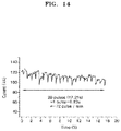
- FIG. 14 illustrates a graph of current converted from a pulse of blood flow at radial artery measured by using a pressure sensor according to an exemplary embodiment
- FIG. 15 illustrates a schematic diagram showing how an experiment was performed in which a pressure sensor according to an exemplary embodiment was compared with a commercially available Phidgets FSR sensor having a diameter of 10 mm, and a graph of a responding property of the two sensors with respect to vibration caused by finger-tapping on a desk;
- FIG. 16 illustrates a graph of current with respect to pressure when a hybrid electronic sheet made from a graphitic material and p8 GB#1 at a ratio of 8:2 transferred on a top substrate of a pressure sensor according to an exemplary embodiment and a hybrid electronic sheet made from a graphitic material and p8 GB#1 at a ratio of 8:2 transferred on a bottom substrate of the pressure sensor were pressed at an incremental pressure rate of 1 kPa, starting from 0 kPa;
- FIG. 17 illustrates a graph of current with respect to pressure when a hybrid electronic sheet made from a graphitic material and p8 GB#1 at a ratio of 2:2 transferred on a top substrate of a pressure sensor according to an exemplary embodiment and a hybrid electronic sheet made from a graphitic material and p8 GB#1 at a ratio of 8:2 transferred on a bottom substrate of the pressure sensor were pressed at an incremental pressure rate of 1 kPa, starting from 0 kPa;
- FIG. 18 illustrates a graph of current with respect to pressure when a hybrid electronic sheet made from a graphitic material and p8 GB#1 at a ratio of 2:2 transferred on a top substrate of a pressure sensor according to an exemplary embodiment and a hybrid electronic sheet made from a graphitic material and p8 GB#1 at a ratio of 2:2 transferred on a bottom substrate of the pressure sensor were pressed at an incremental pressure rate of 1 kPa, starting from 0 kPa;
- FIG. 19 illustrates a graph of current with respect to pressure when a hybrid electronic sheet made from a graphitic material and p8 GB#1 at a ratio of 8:2 transferred on a top substrate of a pressure sensor according to an exemplary embodiment and a hybrid electronic sheet made from a graphitic material and p8 GB#1 at a ratio of 2:2 transferred on a bottom substrate of the pressure sensor were pressed at an incremental pressure rate of 1 kPa, starting from 0 kPa; and
- FIG. 20 illustrates a graph of current when a hybrid electronic sheet made from a graphitic material and p8 GB#1 at a ratio of 5:2 transferred on a top substrate of a pressure sensor according to an exemplary embodiment and poly(3,4-ethylenedioxythiophene) polystyrene sulfonate (PEDOT:PSS) transferred on a bottom substrate were pressed at an incremental pressure rate of 1 kPa, starting from 0 kPa.
- PEDOT:PSS poly(3,4-ethylenedioxythiophene) polystyrene sulfonate
- An aspect provides a pressure sensor including: a bottom substrate; a top substrate located on the bottom substrate and spaced apart from at least a portion of the bottom substrate; and an electronic sheet formed on at least a portion of the bottom substrate or at least a portion of a surface of the top substrate facing the bottom substrate, or a first electronic sheet formed on at least a portion of the bottom substrate and a second electronic sheet formed on at least a portion of a surface of the top substrate facing the bottom substrate; wherein the electronic sheet includes a graphitic material and a phage binding to the graphitic material, and the binding is made between a peptide displayed on a coat protein or a fragment thereof of the phage and the graphitic material.
- pressure sensor used herein may be interchangeably used with “touch sensor” or “tactile sensor,” and refers to an apparatus, tool, or device that detects given force, contact, pressure, tactus, or touch, and converts them into signals (for example, an electric signal).
- the pressure sensor may be a flexible pressure sensor, and may be an integrated or miniaturized pressure sensor having a thickness of less than 1 mm.
- the pressure sensor may have excellent controllable electrical properties, mechanical flexibility, and stability, and due to these properties, the pressure sensor may be used in humanoid robots, touch displays, bio-information measuring wearable devices, smart vehicles, aerial applications, simulation, process control, human-friendly IT, fingerprint recognition systems, or bio-monitoring smart sensors.
- sheet refers to a material having a certain width and a certain thickness, and for example, may include a film, a web, a membrane, or a complex structure thereof.
- graphitic material refers to a material having a surface with a hexagonal arrangement of carbon atoms, i.e., a graphitic surface, and may include any material having a graphitic surface, regardless of physical, chemical or structural properties. Examples thereof are a graphene sheet, a highly oriented pyrolytic graphite (HOPG) sheet, a graphene oxide, a reduced graphene oxide, a carbon nanotube such as a single-walled carbon nanotube, a double-walled carbon nanotube, and a multi-walled carbon nanotube, and fullerene.
- the graphitic material may be metallic, semi-conductive, or a hybrid thereof.
- the graphitic material may be a combination of a graphene sheet and a single-walled carbon nanotube.
- a bottom substrate 104 with a first electronic sheet 101 that has been transferred thereonto, or a top substrate 105 with a second electronic sheet 102 that that has been transferred thereonto may have a pattern.
- the bottom substrate 104 or the top substrate 105 may have a patterned surface having a convex portion and a concave portion, and the convex portion may have a triangular, tetragonal, or circular cross-section.
- the pressure sensor may further include an electrically connected to the electronic sheet 101 , 102 .
- an electrode 103 may be electrically connected to at least one of the first electronic sheet 101 and the second electronic sheet 102 , and may be patterned on the bottom substrate 104 or the top substrate 105 .
- the first electronic sheet 101 may be patterned and transferred between patterns of the electrode 103 on the bottom substrate 104 .
- the electrode 103 is transferred on the bottom substrate 104 , and the first electronic sheet 101 is patterned and transferred on the electrode 103 .
- the first electronic sheet 101 is transferred on the bottom substrate 104 , and the electrode 103 is patterned and transferred on the first electronic sheet 101 .
- the second electronic sheet 102 and the electrode 103 may be disposed on the top substrate 105 in the same manner as described above.
- the pressure sensor may include a conductive material layer formed on the bottom substrate 104 , or on at least a portion of a surface of the top substrate 105 facing the bottom substrate 104 .
- a conductive material layer may be formed on the bottom substrate 104 , or when an electronic sheet is formed on the bottom substrate 104 , a conductive material layer may be formed on at least a portion of a surface of the top substrate 105 facing the bottom substrate 104 .
- the conductive material layer may include a conductive material, and examples thereof will be described below.
- Each of the top substrate 105 and the bottom substrate 104 may be a flexible substrate, for example, a transparent flexible substrate.
- Each of the top substrate 105 and the bottom substrate 104 may be, for example, a substrate manufactured using polydimethylsiloxane (PDMS), polyethersulfone (PES), poly(3,4-ethylenedioxythiophene), poly(styrenesulfonate), polyimide, polyurethane, polyester, perfluoropolyether (PFPE), polycarbonate, or a combination of the forgoing polymers.
- PDMS polydimethylsiloxane
- PES polyethersulfone
- PFPE perfluoropolyether
- a material for the electrode 103 may include a conductive material, for example, silver, silver epoxy, palladium, copper, aluminum, gold, titanium, palladium, chromium, nickel, platinum, silver/silver chloride, silver/silver ion, or mercury/mercury oxide.
- a conductive polymer may be used to form the electrode 103 due to its flexibility and ease of coating.
- a conductive polymer may be used to form the electrode 103 due to its flexibility and ease of coating.
- An example of such a conductive polymer is poly(3,4-ethylenedioxythiophene) polystyrene sulfonate (PEDOT:PSS).
- the pressure sensor may further include a cover 106 located on a surface of the bottom substrate 104 or the top substrate 105 being opposite to where the first and second electronic sheets 101 and 102 are formed.
- the cover 106 may protect or house the pressure sensor, and may be integrally formed with the lower substrate 104 or the top substrate 105 .
- At least a portion of the first electronic sheet 101 formed on a convex portion of the lower substrate 104 may contact at least a portion of the second electronic sheet 102 formed on a convex portion or concave portion of the top substrate 105 .
- at least a portion of the second electronic sheet 102 formed on a convex portion of the top substrate 105 may contact at least a portion of the first electronic sheet 101 formed on a convex portion or concave portion of the lower substrate 104 .
- the bottom substrate 104 or the top substrate 105 may be patterned as described above.
- the contact may occur, for example, between the longest convex portions of two substrates, between side surfaces of convex portions of two substrates, or between the longest convex portion of a substrate and a concave portion of the other substrate. Due to the contact according to an embodiment, the pressure sensor may have high sensitivity and may quickly respond to even shear force.
- the pressure sensor may further include an intermediate insulating structure 107 or an intermediate insulating layer 108 to space the lower substrate 104 from the top substrate 105 .
- the lower substrate 104 and the top substrate 105 may be spaced apart from each other by a certain distance with the intermediate insulating structure 107 or the intermediate insulating layer 108 therebetween.
- the height of the intermediate insulating structure 107 or intermediate insulating layer 108 may be adjusted to be greater than that of the electrode 103 or the first electronic sheet 101 formed on the bottom substrate 104 .
- Pressure applied to the lower substrate 104 , the top substrate 105 , or the cover 106 may change a contact area, contact distance or a conductive network density between the first electronic sheet 101 and the second electronic sheet 102 . Due to the applied pressure, the first electronic sheet 101 and the second electronic sheet 102 , which have been spaced apart from each other, may be brought into contact each other, or in the case in which the first electronic sheet 101 and the second electronic sheet 102 have partly contacted each other, the contact area thereof may increase. Due to the applied pressure, a conductive network of the first electronic sheet 101 may contact a conductive network of the second electronic sheet 102 more.
- the applied pressure may not lead to an increase in the contact area between the first and second electronic sheets 101 and 102 , but their contact distance may be decrease, and their conductive networks may contact each other to a greater degree, resulting in a wider pressure driving range.
- the applied pressure may lead to an increase in the contact area and the conductive network contact between the first and second electronic sheets 101 and 102 , resulting in a higher sensitivity.
- the contact area, contact distance or the conductive network density changes, the resistance or current of a sensor may change, allowing pressure applied to the sensor to be detectable.
- the pressure sensor may measure applied pressure by measuring capacitance.
- capacitance in the case of a pressure sensor including a bottom substrate and a top substrate that are spaced apart from each other without electric contact by an intermediate insulating structure or an intermediate insulating layer, when pressure is applied, capacitance of the pressure sensor changes, and by measuring the change in capacitance, the applied pressure is measured.
- the pressure sensor may include a processor (not shown) that measures a signal (for example, an electric signal) corresponding to applied pressure, or obtains information about, for example, applied pressure.
- the processor may obtain information about force or pressure (for example, intensity of force, direction of force, or how many times force is applied) by measuring varying resistance or current.
- the information may be converted into a certain signal (for example, an electrical signal), which is then displayed, or may be provided to a separate device connected to the pressure sensor so as to allow the separate device to perform a target operation.
- the processor may include an electronic device that converts a measured value into a display value, a display showing results, or one or more control interfaces.
- the pressure sensor may perform the same operation as described in connection with the processor.
- each of the first and second electronic sheets 101 and 102 may have an area of, for example, 0.0001 to 1000 cm 2 , 0.0001 to 100 cm 2 , or 1 to 20 cm2, and a thickness of, for example, 20 to 2000 nm, 40 to 1500 nm, 40 to 1000 nm, 60 to 500 nm, or 80 to 200 nm.
- an internal structure of each of the first and second electronic sheets 101 and 102 including a graphitic material 110 and a phage 120 may have a percolated network structure.
- the term “percolated network” used herein refers to a lattice structure consisting of random conductive or non-conductive linkages.
- Another aspect provides a method of preparing an electronic sheet including: preparing a colloid material including a graphitic material; adding a phage, which displays a peptide having a binding ability to the graphitic material on its coat protein or a fragment thereof, to a solution so as to prepare a phage solution; mixing the colloid material and the phage solution so as to prepare a mixture; and dialyzing the mixture using a membrane so as to form an electronic sheet in a solution.
- the colloid material may be an aqueous solution, in which graphitic materials are dispersed or dissolved.
- the colloid material may be prepared by stabilizing the graphitic material in a surfactant-containing solution.
- the surfactant may include a surfactant which is bio-compatible with biomaterials such as a peptide or a phage. Examples thereof are sodium dodecyl sulfate (SDS), sodium deoxycholate (DOC), Nonidet P-40, Triton X-100, and Tween 20®.
- SDS sodium dodecyl sulfate
- DOC sodium deoxycholate
- Nonidet P-40 Nonidet P-40
- Triton X-100 Triton X-100
- Tween 20® examples thereof are sodium dodecyl sulfate (SDS), sodium deoxycholate (DOC), Nonidet P-40, Triton X-100, and Tween 20®.
- the method of preparing the phage is the same as described above.
- the prepared phage may be added to an appropriate solution, for example, distilled water, phosphate-buffered saline (PBS), or Tris-buffered saline (TBS), and the solution may have a pH of 5 to 8.
- PBS phosphate-buffered saline
- TBS Tris-buffered saline
- a two-dimensional structure of the graphene sheet may provide a large contact area of constituent materials, compared to a material of one-dimensional structure. Therefore, it is possible to realize a large hybrid electronic sheet.
- the concentration of the graphene sheet needs not to be high, which is necessary for when a graphene sheet is used alone, while retaining the advantage of the two-dimensional structure of the graphene sheet.
- the size and thickness of the resultant sheet increase and the effective area of a nanoelectrode per unit area increases.
- a membrane tube containing the mixture may be dialyzed against a dialysis solution, or the mixture may be dialyzed by using a membrane in itself.
- the membrane may include a semi-permeable film or any structure that allows a mixture, such as a material, to permeate therethrough.
- the dialyzing to form the electronic sheet may be dialyzing in an ion-added solution.
- a concentration of ions included in the dialysis solution may be in a range of 0 or more to less than 10 mM.
- the ion concentration may be controllable by adding a monovalent electrolyte to the dialysis solution, for example, 0.1 mM NaCl to triple distilled water used for dialysis.
- the dialysis solution may be distilled water, triple distilled water (resistance>18 Mohm cm), PBS, or TBS in terms of stability with the phage.
- the dialysis may be performed for about 5 to 60 hours, about 10 to 50 hours, or about 15 to 40 hours. After the dialysis, a thin electronic sheet may be formed along the surface of the membrane tube.
- the method of preparing the electronic sheet may further include, after forming the electronic sheet by dialysis, separating the formed electronic sheet from the membrane in an aqueous solution.
- the separation may be accomplished, for example, by twisting the membrane tube used for the dialysis to separate the electronic sheet formed along the membrane.
- a freestanding electronic sheet may be obtained by controlling a membrane clip in an aqueous solution.
- the method of preparing the electronic sheet may further include transferring the electronic sheet formed in the aqueous solution with a suitable substrate or mask according to its purpose.
- the substrate or mask may be made of a metal, a semiconductor, an insulator, a polymer, an elastomer, etc.
- a flexible electronic device may be prepared by transferring the electronic sheet with a flexible polymer substrate.
- this process is to form patterns on the electronic sheet by transferring the separated electronic sheet with a patterned substrate or mask.
- a patterned stencil mask is used, a pattern is formed on the electronic sheet when the mask is detached after the electronic sheet is completely dried.
- a mixing ratio of the colloidal graphitic material and the phage solution may be controlled by those skilled in the art, depending on use of the electronic sheet. That is, the mixing ratio may be controlled depending on the desired properties of the electronic sheet, such as electrical conductivity, electrical conductive properties, electrochemical charging current, hydrophilicity, etc.
- the molar ratio of the colloidal graphitic material and the phage solution may be controlled in terms of structural stability of the electronic sheet, formation of the electronic sheet with a large area, and electrical resistance of the electronic sheet.
- the molar ratio of the colloidal graphitic material and the phage solution may be in a range of 30:1 to 1:30, in a range of 20:1 to 1:20, in a range of 15:1 to 1:15, in a range of 10:1 to 1:10, or in a range of 8:1 to 1:8, for example, 20:1, 10:1, 4:1, 1:4, or 1:8.
- a resistance value of the electronic sheet may be dependent on the molar ratio of the colloidal graphitic material and the phage solution. Accordingly, by controlling the molar ratio, the numbers of the graphitic material and the phage included in the electronic sheet are controlled and thus, a resistance value of the electronic sheet is controlled.
- a ratio of the number of graphitic material to the number of phages included in the electronic sheet in the first electronic sheet or the second electronic sheet may be in a range of 1:10 to 10:1, 1:8 to 8:1, 1:4 to 4:1, or 1:2 to 2:1.
- a resistance value of the first electronic sheet may be equal to or greater than a resistance value of the second electronic sheet.
- a driving range of the pressure sensor may be widened compared to when the resistance value of the first electronic sheet is less than the resistance value of the second electronic sheet.
- the resistance value of the first electronic sheet may be less than the resistance value of the second electronic sheet.
- sensitivity of the pressure sensor may be higher than when the resistance value of the first electronic sheet is equal to or greater than the resistance value of the second electronic sheet.
- the sensitivity of the pressure sensor indicates a minimum level of pressure detectable by a sensor.
- An increased or high sensitivity means that the level of pressure detectable is decreased or low.
- the driving range of the pressure sensor may indicate a range of pressure detectable by a sensor, and an increased or wide driving range of the pressure sensor means that the range of pressure detectable increases or widens.
- sensitivity of the pressure sensor is high, due to high pressure applied to a sensor, the sensor may have a saturated response degree, thereby having a narrow pressure driving range.
- the driving range of the pressure sensor is wide, a response degree of the sensor with respect to applied pressure may less change. Accordingly, even at a high level of pressure, the sensor may measure change in pressure without saturation.
- the method of preparing the electronic sheet enables the manufacture of a nano structure in which a graphitic material and a phage are homogeneously dispersed, and also the manufacture of a large-area flexible electronic sheet having a thickness of 400 nm or less and an area having tens square centimeter.
- the method of preparing the electronic sheet may allow an electronic sheet to be transferred onto various substrates without chemical etching or use of an additional carrier material layer.
- the method of preparing the electronic sheet may provide ease of patterning using a substrate or a mask.
- a peptide binding to the graphitic material may be a material capable of binding to the graphitic material in a nondestructive manner.
- the peptide may be selected from peptide libraries, for example, by a phage display technique. Through the phage display technique, the peptide may be genetically linked to, inserted into, or substituted for the coat protein of the phage, resulting in display of the protein on the exterior of phage, in which the peptide may be encoded by genetic information in the virion. Variants of the protein may be selected and screened by the displayed protein and DNA encoding the same, and this method is called “biopanning”.
- biopanning is carried out by incubating the pool of phage-displayed variants with a target (e.g., graphitic material) that has been immobilized, washing away unbound phage, and eluting specifically bound phage by disrupting the binding interactions between the phage and the target.
- a target e.g., graphitic material
- a portion of the eluted phage is set aside for DNA sequencing and peptide identification, and the remainder is amplified in vivo to prepare a sub-library for the next round. Then, this procedure is repeated.
- phage or “bacteriophage” is used interchangeably, and refers to a virus that infects bacteria and replicates within the bacteria.
- the phage or bacteriophage may be used to display a peptide which selectively or specifically binds to a graphitic material or volatile organic compound.
- the phage may be genetically engineered to display the peptide capable of binding to the graphitic material on a coat protein of the phage or a fragment thereof.
- the term “genetic engineering” or “genetically engineered” means introduction of one or more genetic modifications into the phage in order to display the peptide capable of binding to the graphitic material on the coat protein of the phage or the fragment thereof, or a phage prepared thereby.
- the genetic modifications include introduction of a foreign gene encoding the peptide.
- the phage may be a filamentous phage, for example, M13 phage, F1 phage, Fd phage, If1 phage, Ike phage, Zj/Z phage, Ff phage, Xf phage, Pf1 phage, or Pf3 phage.
- phage display or “phage with a peptide displayed thereon” used herein refers to a display of a functional foreign peptide or protein on the surface of a phage or phagemid particle.
- the surface of the phage may refer to a coat protein of the phage or a fragment thereof.
- the functional foreign peptide may be present as being linked to the N-terminus of the coat protein of the phage, or as being inserted into a coat protein.
- the phage may be a phage in which the C-terminus of a functional foreign peptide is linked to the N-terminus of the coat protein of the phage, or the peptide is inserted between consecutive amino acid sequences of the coat protein of the phage or replaced for a part of the consecutive amino acid sequences of the coat protein.
- the positions in the amino acid sequence of the coat protein, at which the peptide is inserted or replaced, may be positions of 1 to 5, positions of 1 to 40, positions of 1 to 30, positions of 1 to 20, position of 1 to 10, positions of 2 to 8, positions of 2 to 4, positions of 2 to 3, positions of 3 to 4, or a position of 2, from the N-terminus of the coat protein.
- the coat protein may be p3, p6, p8 or p9.
- the peptide having a binding affinity specifically to the graphitic material may be a peptide or a peptide set including one or more selected from the group consisting of amino acid sequences of X 2 SX 1 AAX 2 X 3 P(SEQ ID NO. 1), X 2 X 2 PX 3 X 2 AX 3 P(SEQ ID NO. 2), SX 1 AAX 2 X 3 P(SEQ ID NO. 3), and X 2 PX 3 X 2 AX 3 P(SEQ ID NO. 4).
- the peptide or peptide set may include one or more selected from the group consisting of amino acid sequences of SEQ ID NOS. 5 to 8.
- Consecutive amino acid sequences of a coat protein of a phage may be linked to the N-terminus or C-terminus of the amino acid sequence of the peptide or peptide set. Therefore, for example, the peptide or peptide set may have an amino acid sequence having a length of 5 to 60, 7 to 55, 7 to 40, 7 to 30, 7 to 20, or 7 to 10 amino acids.
- the peptide may have a conservative substitution of a known peptide.
- the peptide may have a conservative substitution of a known peptide.
- the term “conservative substitution” used herein denotes replacement of a first amino acid residue with a second different amino acid residue without changing biophysical properties of a protein or a peptide.
- the first and second amino acid residues mean those having side chains having similar biophysical properties.
- the similar biophysical properties may include an ability to donate or accept hydrophobicity, charge, polarity, or hydrogen bonding.
- Examples of the conservative substitution are within the groups of basic amino acids (arginine, lysine, and histidine), acidic amino acids (glutamic acid and aspartic acid), polar amino acids (glutamine and asparagine), hydrophobic amino acids (leucine, isoleucine, valine and methionine), hydrophilic amino acids (aspartic acid, glutamic acid, asparagine and glutamine), aromatic amino acids (phenylalanine, tryptophan, tyrosine and histidine), and small amino acids (glycine, alanine, serine and threonine).
- Amino acid substitutions that do not generally alter specific activity are known in the art.
- X 1 may be W, Y, F, or H
- X 2 may be D, E, N, or Q
- X 3 may be I, L, or V.
- any one peptide of SEQ ID NO. 1 to SEQ ID NO. 8 may be linked to the body of M13 phage, that is, not to the tip of the phage, but to the N-terminus of p8 (SEQ ID NO. 19) having a length of 50 amino acids, which is present on the body in a longitudinal direction.
- any one peptide of SEQ ID NO. 1 to SEQ ID NO. 8 may be replaced for the positions of 2 to 4 (e.g., EGD), the positions of 2 and 3 or 3 and 4, or the position of 2 in the amino acid sequence of the coat protein p8 of M13 phage.
- a phage that displays a peptide having a binding affinity to a graphitic material specifically bind to the graphitic material, and thus additional functionalities may be provided by a non-destructive method that does not cause damage to properties of the graphitic material.
- a contact area with the graphitic material is large enough to provide a stronger binding affinity.
- the phage may be arranged on the graphitic surface with directionality using the filamentous structure of the phage in itself.
- the phage may be arranged in a row in a specific direction. In this case, the binding affinity of the peptide present on the coat protein of the phage for the graphitic surface is enhanced and the phage is arranged in a row.
- the phage arranged in a row may provide anisotropic functionality to the graphitic surface, which is distinguishable from isotropic or random functionalities which are available when peptide is used alone.
- the phage may be arranged to form a structure having specific directionality, such as a layered (e.g., smectic), nematic, spiral or lattice structure. Accordingly, various functionalities may be provided onto the graphitic surface using the arrangement structures of the phage.
- the pressure sensor may be a pressure sensor for measuring blood pressure or a heart rate.
- the blood pressure may be arterial pressure, capillary blood pressure, or venous pressure, and in general, the blood pressure may mean arterial pressure.
- the arterial pressure changes corresponding to cardiac impulse.
- the blood pressure may be measured in an invasive manner or a non-invasive manner.
- the pressure sensor may be connected to a catheter to measure blood pressure.
- a catheter is inserted into a blood vessel to measure blood pressure through a connector containing, for example, a Heparin isotonic sodium chloride solution.
- the pressure sensor is connected to a front end of the catheter to measure blood pressure.
- the pressure sensor may be located on a site where a pulse wave is measurable, for example, a soft skin site where the radial artery, the brachial artery, the carotid artery, the carotid vein, the femoral artery, the popliteal artery, the tibial artery, or the dorsal pedis artery runs.
- the pressure sensor may measure blood pressure by detecting the pressure (e.g. blood pressure) delivered to a skin site located above the blood vessel when the heart pulses and the blood vessel shrinks or expands.
- the pressure sensor may measure a heart impulse or a heart rate by detecting a pulse occurring in a blood vessel or vein when the heart pulses and converting the pulse into an electric signal.
- a wearable device including a pressure sensor, the pressure sensor including: a bottom substrate; a top substrate located on the bottom substrate and spaced apart from at least a portion of the bottom substrate; and an electronic sheet formed on at least a portion of the bottom substrate or at least a portion of a surface of the top substrate facing the bottom substrate, or a first electronic sheet formed on at least a portion of the bottom substrate and a second electronic sheet formed on at least a portion of a surface of the top substrate facing the bottom substrate; wherein the electronic sheet includes a graphitic material and a phage binding to the graphitic material, and the binding is made between a peptide displayed on a coat protein or a fragment thereof of the phage and the graphitic material.
- the pressure sensor is the same as described above.
- the wearable device is used to measure bio-information, and the bio-information may include blood pressure or a heart rate.
- the bio-information may be force or pressure generated by walking
- one or more pressure sensors may be mounted on the sole of a person's foot or footwear to measure the intensity or distribution degree of force caused by walking.
- one or more pressure sensors may be mounted on a person's tooth or oral cavity to measure degree of force or distribution due to a tooth bite.
- the wearable device may be a patch, a band, a watch, footwear, tooth attached device.
- the wearable device may further include a controller that logically communicates with the pressure sensor, and receives and processes signal data generated by the pressure sensor so as to output data associated with controlling the pressure sensor.
- the pressure sensor of the wearable device may be controlled by the controller, which responds at certain time intervals or responds to a particular event (for example, a switch operation) and receives and processes bio-information detected by the pressure sensor.
- a particular event for example, a switch operation
- the wearable device may further include a memory that stores a processor for operation of a controller, and that temporally stores input/output data (for example, bio-information).
- the memory may store information (for example, blood pressure or heart rate) about electrical signals transmitted by the pressure sensor.
- the wearable device may further include a display unit that displays information processed by the controller or information stored by the memory.
- the wearable device may further include a wireless communication unit that sends information processed by the controller or information stored by the memory to a person wearing the wearable device or other users (for example, a person located near the person wearing the wearable device, a trainer of athletes, a physician, a hospital, or the family of the person wearing the wearable device) all having a wireless communication system.
- the wireless communication unit may include a broadcasting receiving module, a mobile communication module, a wireless Internet module, or a near-distance communication module. Information detected by the pressure sensor may be sent to the person wearing the wearable device including the pressure sensor or other users through the wireless communication unit.
- the pressure sensor has excellent controllable electric properties, and mechanical flexibility and stability, and accordingly, the pressure sensor is effectively used in the wearable device configured to measure bio-information (for example, blood pressure or heart rate).
- bio-information for example, blood pressure or heart rate
- an aqueous solution was prepared by adding 2% w/v sodium cholate as a surfactant to distilled water, and a colloid solution was prepared by stabilizing single-walled carbon nanotubes with the sodium cholate by dialysis of carbon nanotubes (manufacturer: Nanointegris, SuperPure SWNTs, solution-type, concentration: 250 mg/ml) for 48 hours.
- the number of the single-walled carbon nanotube included in the colloid solution was 7.5 ⁇ 10 13 /mL.
- an M13 phage (p8 GB#1) displaying a peptide DSWAADIP (SEQ ID NO. 5) having a strong binding affinity to the graphitic surface and an M13 phage (p8 GB#5) displaying a peptide DNPIQAVP (SEQ ID NO. 6) were prepared by the following method.
- an M13HK vector was prepared using oligonucleotides of SEQ ID NOS. 10 and 11 for site-directed mutation of the 1381st base pair C of an M13KE vector (NEB, product #N0316S) (SEQ ID NO. 9) to G.
- the prepared M13HK vector was double-digested using restriction enzymes, BspHI (NEB, product #R0517S) and BamHI (NEB, product #R3136T), and dephosphorylated using antarctic phosphatase.
- the dephosphorylated vector was ligated to a double-digested DNA duplex by incubation at 16° C. overnight. A product is then purified and concentrated.
- Electrocompetent cells (XL-1 Blue, Stratagene) were transformed with 2 ⁇ l of a concentrated ligated vector solution by electroporation at 18 kV/cml. A total of five transformations were performed for the library construction. Then, the transformed cells were incubated for 60 minutes, and fractions of several transformants were plated onto agar plates containing x-gal/isopropyl- ⁇ -D-1-thiogalactopyranoside (IPTG)/tetracycline (Tet) to determine the diversity of the library. The remaining cells were amplified in a shaking incubator for 8 hours. Oligonucleotides of SEQ ID NOS. 12 and 13 were used in construction of the phage-display p8 peptide library.
- the base sequences of the phage-display p8 peptide library constructed according to an exemplary embodiment had diversity of 4.8 ⁇ 10 7 pfu (plaque forming unit), and include approximately 1.3 ⁇ 10 5 copies of each sequence.
- HOPG highly ordered pyrolytic graphite
- SPI product #439HP-AB pyrolytic graphite
- the HOPG substrate was a HOPG substrate having a relatively large grain size of 100 ⁇ m or smaller.
- a carbon nanotube film surface damaged during its production process had been generally used as a graphitic surface, and thus it was difficult to identify peptides having high binding affinity.
- HOPG as a material having a graphitic surface was detached from a substrate by using a tape immediately before use, thereby obtaining a fresh surface, so as to minimize the occurrence of defects caused by, for example, oxidation.
- the phage display p8 peptide library of 4.8 ⁇ 10 10 pfu (4.8 ⁇ 10 7 diversities, 1000 copies per each sequence), prepared as described above, was prepared in 100 ⁇ L of tris-buffered saline (TBS) and conjugated with the HOPG surface for 1 hour in a shaking incubator at 100 rpm. 1 hour later, the solution was removed and the surface was washed 10 times in TBS. The washed HOPG surface was reacted with Tris-HCl of pH 2.2 as an acidic buffer for 8 minutes to elute peptides reacting non-selectively, and the remaining phage was eluted with an XL-1 blue E. coli culture in mid-log phase for 30 minutes.
- TBS tris-buffered saline
- a portion of the eluted culture was set aside for DNA sequencing and peptide identification, and the remainder was amplified to prepare a sub-library for the next round. The above procedure was repeated using the prepared sub-library. Meanwhile, the left plaque was subjected to DNA sequencing to obtain the p8 peptide sequence, and the sequence was analyzed to obtain a phage (P8 GB#1) with DSWAADIP (SEQ ID NO: 5) displayed thereon and a phage (p8 GB#5) with DNPIQAVP(SEQ ID NO: 6) displayed thereon.
- DSWAADIP SEQ ID NO: 5
- DNPIQAVP(SEQ ID NO: 6) were peptide sequences having a strong binding affinity to a graphitic material.
- an aspartic acid (D) which is a first amino acid sequence from the N-termini of SEQ ID NOS. 5 and 6, does not affect the binding, and a phage with peptide sequences of SWAADIP(SEQ ID NO. 7) and NPIQAVP(SEQ ID NO. 8) displayed thereon was obtained to confirm its binding to a graphitic material.
- the colloid solution prepared above and a phage solution containing the M13 phage (p8 GB#1) having a strong binding force to the graphitic material were mixed at a molar ratio of 8:2.
- the mixture was added to a semipermeable dialysis membrane (SpectrumLab, MWCO 12,000 to 14,000, product #132 700) tube, and the membrane tube was dialyzed against triple distilled water. About 16 hours after the dialysis began, a thin electronic sheet was formed along the surface of the membrane tube. Next, the membrane tube was transferred to triple distilled water and the electronic sheet was detached by twisting the membrane of the membrane tube and then dried.
- a semipermeable dialysis membrane SpectrumLab, MWCO 12,000 to 14,000, product #132 700
- FIG. 9 illustrates how to manufacture a hybrid electronic sheet of a pressure sensor according to an exemplary embodiment.
- a PDMS polymer substrate was used as a bottom substrate.
- Sylgard® 184 silicon elastomer and a Sylgard® 184 silicon elastomer curing agent were mixed at a ratio of 10:1, and then, a thickness of the result was adjusted by petri-dish spin coating, and curing was performed thereon in an oven at a temperature of 70° C. for about 6 hours.
- the cured PDMS film was cut to a desired size by using a knife for surgery.
- a Stencil mask was mounted, and then, a metal electrode (Pt) was placed thereon by sputtering.
- the hybrid electronic sheet prepared according to Example 1.3 was transferred on by using a stencil mask having a size of 1.5 ⁇ 1.5 cm, and then dried in air for about 1 hour.
- the resultant dried substrate with the hybrid electronic sheet electrode transferred thereon was used as a bottom substrate for a flexible pressure device.
- a mould for a patterned polymer substrate for use as a top substrate was manufactured.
- SU-8 100 manufactured by Microchem Company
- SU-8 100 was spin-coated on a silicon wafer at a rotational rate of 3000 rpm, and then, sequentially cured at a temperature of 60° C. for 30 minutes and then, at a temperature of 90° C. for 60 minutes, and then, ultraviolet (UV) light was irradiated thereto through a mask having a target pattern and a mask aligner.
- a target pattern thickness was adjusted by controlling the thickness of a SU-8 film.
- a width of a line pattern was designed to be in a range of 200 to 400 ⁇ m.
- the result was cured at a temperature of 60° C. for about 1 minutes, and then, at a temperature of 90° C. for about 20 minutes, and then, the formed pattern was developed by using a developer dedicated for SU-8 only (manufactured by Microchem Company).
- the silicon wafer with a pattern thereon was used as a mould.
- the line pattern formed as described above or a box pattern was formed by using photoresist, and then, an outer wall of a polymer was melted by using a polymer reflow method, thereby completing the manufacture of a round silicon mould.
- a tetragonal concave pattern was formed on a silicon wafer by using a photoresist, and a portion of the silicon wafer corresponding to the tetragonal concave pattern that was not protected by the photoresist was etched by using a silicon etching solution (HF), thereby completing the manufacture of a pyramid-shape concave pattern.
- HF silicon etching solution
- FIG. 10 illustrates the top substrate of a pressure sensor according to an exemplary embodiment with the hybrid electronic sheet transferred thereon.
- the hybrid electronic sheet can be conformally formed even on a substrate having a step.
- an epoxy curing agent/a polyacrylate polymer adhesive were used to contact the two PDMS polymer substrates.
- the pressure sensor according to an exemplary embodiment may be a large-area flexible pressure sensor device having a thickness of 1 mm or less.
- Performance of the manufactured pressure sensor was measured by using a 4156A precision semiconductor parameter analyzer manufactured by HP Company. Different pressures were applied to the manufactured pressure sensor and a voltage of ⁇ 1V to +1V was applied to two electrodes to measure I-V (current vs. voltage) signals according to pressure, and results thereof are shown in FIGS. 11 and 12 .
- FIG. 11 is a graph of current when different levels of pressure are applied to a pressure sensor according to an exemplary embodiment.
- FIG. 12 is a graph of current when a pressure sensor according to an exemplary embodiment is pressed or released.
- FIG. 13 illustrates a graph of change in current of the pressure sensor over time caused by force generated by the finger-tapping.
- the current promptly increases and decreases, and the response speed of the flexible pressure sensor with respect to the finger-tapping is 50 ms or less.
- This experiment was performed to confirm whether the manufactured pressure device can be as a wearable device.
- a voltage of 2 V was applied between two electrodes, and flexible pressure devices were attached on the wrist where radial artery runs and the neck where carotid vein runs to measure change in blood pressure, and results thereof are shown in FIG. 14 .
- FIG. 14 illustrates a graph of current converted from a pulse of blood flow at radial artery measured by using a pressure sensor according to an exemplary embodiment.
- the manufactured pressure device was compared with a commercially available force sensitive resistor (FSR)-based pressure sensor to analyze a responding property thereof.
- FSR force sensitive resistor
- a hybrid electronic sheet-based flexible pressure device was stacked on a Philgets FSR sensor having a diameter of 10 mm, and then, a 1 kg (about 100 kPa) weight was placed on these two sensors. Then, a surrounding area thereof was tapped by using a finger and at this time, and the resistance of the sensors was measured. Results thereof are shown in FIG. 15 .
- FIG. 15 illustrates a schematic diagram showing how an experiment was performed in which a pressure sensor according to an exemplary embodiment was compared with a commercially available Phidgets FSR sensor having a diameter of 10 mm, and a graph of a responding property of the two sensors with respect to vibration caused by finger-tapping on a desk.
- the sensors commonly showed a decrease in resistance due to vibration caused by tapping in the same period.
- the decrease in resistance to micro vibration caused by finger-tapping the pressure sensor according to an exemplary embodiment was about 7 times as high as that of the FSR sensor, and accordingly, it is seen that the pressure sensor according to an exemplary embodiment is more sensitive to vibration than the FSR sensor. That is, it is seen that the pressure sensor manufactured using a hybrid electronic sheet including a highly conductive/functional carbon nanotube was a highly-sensitive flexible pressure sensor that responds to even small change in pressure compared to the metal/polymer-based commercially available FSR sensor.
- a resistance-change pressure sensor operates based on change in resistance thereof according to change in a contact area between a top substrate and a bottom substrate occurring when the pressure sensor is pressed. Accordingly, it is possible that sensitivity of a pressure sensor is controllable by changing electrical characteristics of a top substrate and a bottom substrate. To do this, hybrid electronic sheets having different electric characteristics were prepared and placed on the top substrate or the bottom substrate of the pressure sensor.
- pressure sensors were manufactured in the same manner as in Example 1, except that when the hybrid electron sheets for the top substrate and the bottom substrate were prepared, the phage solution including the colloid solution and the M13 phage(p8 GB#1) were prepared at molar ratios shown in Table 1.
- the resistance of a hybrid electronic sheet with respect to an electrode was measured as follows: a hybrid electronic sheet was transferred between two electrodes on a bottom substrate for a pressure sensor by using a stencil mask having a size of 2 ⁇ 2 mm and the resistance of the hybrid electronic sheet was measured by using a Fluke multi-meter.
- the small pressure sensor according to an exemplary embodiment can be 55 times as small as the pressure sensor manufactured according to Example 1.3.
- a hybrid electronic sheet according to an exemplary embodiment enables manufacture of an integrated and miniaturized pressure sensor.
- FIG. 16 illustrates a graph of current with respect to pressure when a hybrid electronic sheet made from the graphitic material and p8 GB#1 at a ratio of 8:2 and transferred on a top substrate of a pressure sensor according to an exemplary embodiment and a hybrid electronic sheet made from the graphitic material and p8 GB#1 at a ratio of 8:2 and transferred on a bottom substrate of the pressure sensor were pressed at an incremental pressure rate of 1 kPa, starting from 0 kPa.
- FIG. 17 illustrates a graph of current with respect to pressure when a hybrid electronic sheet made from the graphitic material and p8 GB#1 at a ratio of 2:2 and transferred on a top substrate of a pressure sensor according to an exemplary embodiment and a hybrid electronic sheet made from the graphitic material and p8 GB#1 at a ratio of 8:2 and transferred on a bottom substrate of the pressure sensor were pressed at an incremental pressure rate of 1 kPa, starting from 0 kPa.
- the pressure sensor including the top substrate made from the graphitic material and p8 GB#1 at a ratio of 8:2 and the bottom substrate made from the graphitic material and p8 GB#1 at a ratio of 8:2, when a voltage of 1 kPa was applied to the pressure sensor, the current was increased by about 15%.
- the flexible pressure sensor that includes the top substrate with the hybrid electronic sheet formed using the graphitic material and p8 GB#1 at a ratio of 2:2 and transferred thereon and the bottom substrate with the hybrid electronic sheet formed using the graphitic material and p8 GB#1 at a ratio of 8:2 and transferred thereon, when a voltage of 1 kPa was applied to the pressure sensor, the current was increased by about 1%.
- FIG. 18 illustrates a graph of current with respect to pressure when a hybrid electronic sheet made from the graphitic material and p8 GB#1 at a ratio of 2:2 and transferred on a top substrate of a pressure sensor according to an exemplary embodiment and a hybrid electronic sheet made from the graphitic material and p8 GB#1 at a ratio of 2:2 transferred on a bottom substrate of the pressure sensor were pressed at an incremental rate of 1 kPa, starting form 0 kPa.
- FIG. 19 illustrates a graph of current with respect to pressure when a hybrid electronic sheet made from the graphitic material and p8 GB#1 at a ratio of 8:2 and transferred on a top substrate of a pressure sensor according to an exemplary embodiment and a hybrid electronic sheet made from the graphitic material and p8 GB#1 at a ratio of 2:2 and transferred on a bottom substrate of the pressure sensor were pressed at an incremental rate of 1 kPa, starting from 0 kPa.
- the sensitivity and driving range of a flexible pressure sensor are controllable by adjusting a composition of a hybrid electronic sheet.
- the results also show that in a pressure sensor according to an exemplary embodiment, when a top substrate is pressed, the top substrate is brought into contact with a bottom substrate, leading to a lower resistance and a higher current in the pressure sensor. This means that a driving range of the flexible pressure sensor is controllable by changing the strength or pattern structure of the top substrate.
- a pressure sensor including a hybrid electronic sheet transferred only on a top substrate
- a pressure sensor was manufactured in the same manner as used to manufacture the pressure sensor 1 , except that a conductive polymer was coated on the bottom substrate.
- a PDMS polymer substrate was used as the bottom substrate.
- Sylgard® 184 silicon elastomer and a Sylgard® 184 silicon elastomer curing agent were mixed at a ratio of 10:1, and then, a thickness of the result was adjusted by petri-dish spin coating, and curing was performed thereon in an oven at a temperature of 70° C. for about 6 hours.
- the cured PDMS film was cut to a desired size by using a knife for surgery.
- a Stencil mask On the separated flexible polymer PDMS film, a Stencil mask was mounted, and then, a metal electrode (Pt) was placed thereon by sputtering. A PEDOT:PSS solution was dropped portionwise between deposited two electrodes, and then, spin coating was performed thereon at a 3000 rpm to complete the manufacture of the bottom substrate having conductivity. For stability of the bottom substrate, the bottom substrate was heat treated in an oven at a temperature of 80° C. for about 10 minutes.
- a top substrate having a pyramid structure was manufactured by silicon wafer etching.
- a silicon substrate was patterned by using an exposure process to have a tetragonal pattern, and buffered oxide etching (BOE) was performed thereon for 10 minutes to remove silicon oxide, and then, 30% KOH etching was performed thereon to manufacture a pyramid structure.
- a height of the pyramid structure was about 100 um.
- Sylgard® 184 silicon elastomer and Sylgard® 184 silicon elastomer curing agent were mixed at a ratio of 10:1, and then, a petridish spin coating method was used to adjust the thickness of the resultant. Then, in an oven at a temperature of 70° C., curing was performed thereon for about 6 hours.
- the hardened PDMS film was cut to a target size by using an operating knife.
- a hybrid electronic sheet made from a graphitic material and p8 GB#1 at a ratio of 5:2 was transferred onto the top substrate having the pyramid structure by using a stencil mask, and then, dried for about one hour in air.
- the hybrid electronic sheet transferred on the polymer film of the top substrate was washed with distilled water after removing the stencil mask, and then dried by using nitrogen gas. Then, the bottom substrate with PEDOT:PSS coated thereon was folded with the top substrate with the hybrid electronic sheet coated thereon, the resultant structure was packaged by using a polymer material having sticky properties, thereby completing manufacture of a flexible pressure device.
- a PDMS solution was doped on outside a top/bottom substrate PDMS substrate, and then cured at a temperature of 80° C. for about 30 minutes.
- an epoxy curing agent/a polyacrylate polymer adhesive were used to bind two PDMS polymer substrates together.
- a current change with respect to pressure was measured in such a way that 0-10 V of voltage was applied to two electrodes of the pressure sensor 5 , while 0 to 5 kPa of pressure was applied thereto at an incremental rate of 1 kPa. Results thereof are shown in FIG. 20 .
- FIG. 20 illustrates a graph of current when 0 to 1 kPa of pressure was incrementally applied to a pressure sensor according to an embodiment including a top substrate with a hybrid electronic sheet made from graphitic material and p8 GB#1 at a ratio of 5:2 and transferred thereon and a bottom substrate having PEDOT:PSS transferred thereon.
- Pressure sensors according to embodiments have excellent controllable electric properties, and mechanical flexibility and stability, and can be used to measure, for example, pressure in an easy and highly reproducible manner in which resistance of a component in the pressure sensor is changed when pressure is applied thereto.
Abstract
Description
Number of single-walled carbon nanotubes (number/mL)=concentration (μg/mL)×3×1011 CNT [Equation 1]
| TABLE 1 | |||||
| Pressure | Pressure | | Pressure | ||
| sensor | |||||
| 1 | |
sensor 3 | |
||
| Top substrate | 8:2 | 2:2 | 2:2 | 8:2 | ||
| Bottom | 8:2 | 8:2 | 2:2 | 2:2 | ||
| substrate | ||||||
Claims (18)
Applications Claiming Priority (2)
| Application Number | Priority Date | Filing Date | Title |
|---|---|---|---|
| KR20150046751 | 2015-04-02 | ||
| KR10-2015-0046751 | 2015-04-02 |
Publications (2)
| Publication Number | Publication Date |
|---|---|
| US20160287089A1 US20160287089A1 (en) | 2016-10-06 |
| US10568579B2 true US10568579B2 (en) | 2020-02-25 |
Family
ID=57015033
Family Applications (1)
| Application Number | Title | Priority Date | Filing Date |
|---|---|---|---|
| US14/988,459 Active 2037-07-27 US10568579B2 (en) | 2015-04-02 | 2016-01-05 | Pressure sensor including hybrid electronic sheet and wearable device including the pressure sensor |
Country Status (3)
| Country | Link |
|---|---|
| US (1) | US10568579B2 (en) |
| KR (1) | KR101878358B1 (en) |
| CN (1) | CN106052943B (en) |
Cited By (1)
| Publication number | Priority date | Publication date | Assignee | Title |
|---|---|---|---|---|
| US20200069193A1 (en) * | 2016-03-31 | 2020-03-05 | The Regents Of The University Of California | Soft capacitive pressure sensors |
Families Citing this family (24)
| Publication number | Priority date | Publication date | Assignee | Title |
|---|---|---|---|---|
| US10289230B2 (en) * | 2014-05-20 | 2019-05-14 | Iucf-Hyu (Industry-University Cooperation Foundation Hanyang University) | Graphene touch sensor, method for operating same, and method for manufacturing same |
| US20160100778A1 (en) * | 2014-10-10 | 2016-04-14 | Korea Institute Of Science And Technology | Biosensor and wearable device for detecting bioinformation including hybrid electronic sheet |
| WO2017149499A1 (en) * | 2016-03-04 | 2017-09-08 | King Abdullah University Of Science And Technology | 3d noncontact humidity sensing technologies and methods of use thereof |
| KR102525201B1 (en) * | 2016-03-22 | 2023-04-25 | 삼성디스플레이 주식회사 | Flexible electronic device |
| WO2018120226A1 (en) * | 2016-12-30 | 2018-07-05 | 华为技术有限公司 | Method for preparing capacitor and capacitor |
| WO2018167077A1 (en) * | 2017-03-13 | 2018-09-20 | Holger Redtel | Apparatus and method for measuring the cardiac pulse of a living being |
| US20200121201A1 (en) * | 2017-03-13 | 2020-04-23 | Heiko Redtel | Method and device for the time-resolved measurement of characteristic variables of the cardiac function |
| US11331019B2 (en) | 2017-08-07 | 2022-05-17 | The Research Foundation For The State University Of New York | Nanoparticle sensor having a nanofibrous membrane scaffold |
| CZ31541U1 (en) * | 2017-08-15 | 2018-03-06 | Univerzita Tomáše Bati ve Zlíně | Smart footwear with a comprehensive system of monitoring data of its user |
| KR102001656B1 (en) * | 2017-11-07 | 2019-10-01 | 울산과학기술원 | Joint device for robot based on compliant mechanism and manufacturing method of the same |
| KR102520722B1 (en) * | 2018-04-05 | 2023-04-11 | 삼성디스플레이 주식회사 | Force sensor |
| JP2021521451A (en) | 2018-04-16 | 2021-08-26 | オーピクス メディカル テクノロジーズ インコーポレイテッド | High resistance sensor and how to use it |
| CN108981980A (en) * | 2018-05-03 | 2018-12-11 | 五邑大学 | A kind of nanoscale rotary table microstructure pressure sensor and preparation method thereof |
| CN108917995A (en) * | 2018-05-15 | 2018-11-30 | 浙江工业大学 | A kind of flexibility piezoresistance sensor |
| KR102086417B1 (en) | 2018-08-17 | 2020-03-09 | 포항공과대학교 산학협력단 | Pixel-type pressure sensor and method for preparing the same |
| KR102147274B1 (en) * | 2019-02-11 | 2020-08-24 | 연세대학교 산학협력단 | Strain sensor including patterned nanomaterial and method of manufacturing the same |
| KR102204967B1 (en) * | 2019-03-08 | 2021-01-19 | 한국전자기술연구원 | Flexible pressure sensor and a method for making the same |
| WO2020214808A1 (en) * | 2019-04-17 | 2020-10-22 | The Regents Of The University Of California | Scalable and high-performance pressure sensors for wearable electronics |
| CN113873940A (en) * | 2019-05-06 | 2021-12-31 | Sen运动有限公司 | Sensor element, sensor device, sensor system and method for detecting a force between a foot and a support surface |
| CN111283690B (en) * | 2020-01-16 | 2022-09-09 | 中国科学院重庆绿色智能技术研究院 | Elastic bionic villus type electronic skin for human-computer interaction safety |
| CN112362199B (en) * | 2020-10-30 | 2022-07-19 | 华中科技大学 | Medium insertion type capacitive pressure sensor and preparation method thereof |
| CN113093588B (en) * | 2021-03-09 | 2022-06-24 | 青岛大学 | Fabric-based flexible control system and method |
| KR102629244B1 (en) * | 2021-11-09 | 2024-01-24 | 중앙대학교 산학협력단 | Wearable sensor and manufacturing method of the wearable sensor |
| LU502480B1 (en) | 2022-07-07 | 2024-01-09 | Innovationlab Gmbh | Sensor with microstructure |
Citations (25)
| Publication number | Priority date | Publication date | Assignee | Title |
|---|---|---|---|---|
| JPH01253627A (en) | 1988-04-01 | 1989-10-09 | Res Dev Corp Of Japan | Pressure sensor and manufacture thereof |
| WO1996026674A1 (en) | 1995-02-27 | 1996-09-06 | Medtronic, Inc. | Implantable capacitive absolute pressure and temperature monitor system |
| WO1999020649A1 (en) | 1997-10-22 | 1999-04-29 | Merck Patent Gmbh | Spacer peptides and membranes containing same |
| US20050147964A1 (en) | 2003-12-30 | 2005-07-07 | Intel Corporation | Methods for identifying a peptide that binds a geometrical shape |
| WO2006060226A1 (en) | 2004-12-02 | 2006-06-08 | Honeywell International Inc. | Disposable pressure sensor with variable inductance and/or variable capacitance resulting in resonance frequency variations |
| US20060287602A1 (en) * | 2005-06-21 | 2006-12-21 | Cardiomems, Inc. | Implantable wireless sensor for in vivo pressure measurement |
| US20070117147A1 (en) | 2002-06-04 | 2007-05-24 | Anand Jagota | Carbon nanotube binding peptides |
| US20070264623A1 (en) | 2004-06-15 | 2007-11-15 | President And Fellows Of Harvard College | Nanosensors |
| US20070281321A1 (en) | 2006-05-31 | 2007-12-06 | Esa Biosciences, Inc. | Biosensor for measurement of species in a body fluid |
| US20080087543A1 (en) | 2006-10-11 | 2008-04-17 | Infopia Co., Ltd. | Biosensor |
| US7574792B2 (en) * | 2003-09-16 | 2009-08-18 | Cardiomems, Inc. | Method of manufacturing an implantable wireless sensor |
| KR20100079579A (en) | 2008-12-31 | 2010-07-08 | 키스트 유럽 에프게엠베하 | Manufacturing method of bactriophage in which molecular recognition material is arranged and using method of the same for detecting extremely small quantities and mass analysis device using the same |
| CN201622147U (en) | 2010-03-01 | 2010-11-03 | 苏州日精仪器有限公司 | Integrated capacitor type pressure sensor |
| US20110053737A1 (en) * | 2009-08-31 | 2011-03-03 | Industrial Technology Research Institute | Pressure sensor and boxing machine using the same |
| CN102308270A (en) | 2009-02-06 | 2012-01-04 | 压力分布系统公司 | Capacitive proximity tactile sensor |
| US8161826B1 (en) * | 2009-03-05 | 2012-04-24 | Stryker Corporation | Elastically stretchable fabric force sensor arrays and methods of making |
| KR20120053797A (en) | 2010-11-18 | 2012-05-29 | 경희대학교 산학협력단 | Electrode for electrochemical biosensor and biosensor including the same |
| US20120245444A1 (en) | 2007-11-07 | 2012-09-27 | University Of Washington | Wireless powered contact lens with glucose sensor |
| US20130053666A1 (en) | 2011-08-26 | 2013-02-28 | Dexcom, Inc. | Polymer membranes for continuous analyte sensors |
| WO2013052318A1 (en) | 2011-09-25 | 2013-04-11 | Theranos, Inc. | Systems and methods for multi-analysis |
| US20140174927A1 (en) | 2011-07-27 | 2014-06-26 | Rashid Bashir | Nanopore Sensors for Biomolecular Characterization |
| US20140249052A1 (en) | 2011-10-24 | 2014-09-04 | University Of Washington Through Its Center For Commercialization | Polypeptides and their use |
| US9493764B2 (en) | 2014-04-22 | 2016-11-15 | Korea Institute Of Science And Technology | Hybrid electronic sheets |
| US20170204400A1 (en) | 2014-09-26 | 2017-07-20 | The Board Of Trustees Of The University Of Illinois | Biosynthesis and engineering of lanthipeptides |
| US10017537B2 (en) | 2013-04-15 | 2018-07-10 | Korea Institute Of Science And Technology | Peptide selectively binding to graphitic materials and volatile organic compounds |
Family Cites Families (4)
| Publication number | Priority date | Publication date | Assignee | Title |
|---|---|---|---|---|
| JP5887947B2 (en) | 2011-03-28 | 2016-03-16 | ソニー株式会社 | Transparent conductive film, heater, touch panel, solar cell, organic EL device, liquid crystal device, and electronic paper |
| KR101636695B1 (en) * | 2014-08-18 | 2016-07-06 | 연세대학교 산학협력단 | Bio sensor using three-dimensional graphene-silk complex and sensing system using the same |
| KR101798295B1 (en) * | 2015-11-05 | 2017-11-17 | 성균관대학교산학협력단 | Manufacturing method of biosensor platform using graphene and protein, biosensor platform made by the same, and field effect transistor type biosensor comprising the same |
| KR101987363B1 (en) * | 2016-09-30 | 2019-06-11 | 한국과학기술연구원 | Pressure sensor comprising layer of discontinuous conductive patterns, device comprising the same, and apparatus and method for detecting pressure |
-
2015
- 2015-12-28 KR KR1020150187641A patent/KR101878358B1/en active IP Right Grant
-
2016
- 2016-01-05 US US14/988,459 patent/US10568579B2/en active Active
- 2016-01-29 CN CN201610065711.6A patent/CN106052943B/en active Active
Patent Citations (28)
| Publication number | Priority date | Publication date | Assignee | Title |
|---|---|---|---|---|
| JPH01253627A (en) | 1988-04-01 | 1989-10-09 | Res Dev Corp Of Japan | Pressure sensor and manufacture thereof |
| WO1996026674A1 (en) | 1995-02-27 | 1996-09-06 | Medtronic, Inc. | Implantable capacitive absolute pressure and temperature monitor system |
| WO1999020649A1 (en) | 1997-10-22 | 1999-04-29 | Merck Patent Gmbh | Spacer peptides and membranes containing same |
| US20070117147A1 (en) | 2002-06-04 | 2007-05-24 | Anand Jagota | Carbon nanotube binding peptides |
| US7574792B2 (en) * | 2003-09-16 | 2009-08-18 | Cardiomems, Inc. | Method of manufacturing an implantable wireless sensor |
| US20050147964A1 (en) | 2003-12-30 | 2005-07-07 | Intel Corporation | Methods for identifying a peptide that binds a geometrical shape |
| US20070264623A1 (en) | 2004-06-15 | 2007-11-15 | President And Fellows Of Harvard College | Nanosensors |
| CN101111750A (en) | 2004-12-02 | 2008-01-23 | 霍尼韦尔国际公司 | Disposable pressure sensor with variable inductance and/or variable capacitance resulting in resonance frequency variations |
| WO2006060226A1 (en) | 2004-12-02 | 2006-06-08 | Honeywell International Inc. | Disposable pressure sensor with variable inductance and/or variable capacitance resulting in resonance frequency variations |
| US20060287602A1 (en) * | 2005-06-21 | 2006-12-21 | Cardiomems, Inc. | Implantable wireless sensor for in vivo pressure measurement |
| US20070281321A1 (en) | 2006-05-31 | 2007-12-06 | Esa Biosciences, Inc. | Biosensor for measurement of species in a body fluid |
| US20080087543A1 (en) | 2006-10-11 | 2008-04-17 | Infopia Co., Ltd. | Biosensor |
| US20120245444A1 (en) | 2007-11-07 | 2012-09-27 | University Of Washington | Wireless powered contact lens with glucose sensor |
| KR20100079579A (en) | 2008-12-31 | 2010-07-08 | 키스트 유럽 에프게엠베하 | Manufacturing method of bactriophage in which molecular recognition material is arranged and using method of the same for detecting extremely small quantities and mass analysis device using the same |
| US8627716B2 (en) | 2009-02-06 | 2014-01-14 | Pressure Profile Systems Inc. | Capacitive proximity tactile sensor |
| CN102308270A (en) | 2009-02-06 | 2012-01-04 | 压力分布系统公司 | Capacitive proximity tactile sensor |
| US8161826B1 (en) * | 2009-03-05 | 2012-04-24 | Stryker Corporation | Elastically stretchable fabric force sensor arrays and methods of making |
| US20110053737A1 (en) * | 2009-08-31 | 2011-03-03 | Industrial Technology Research Institute | Pressure sensor and boxing machine using the same |
| CN201622147U (en) | 2010-03-01 | 2010-11-03 | 苏州日精仪器有限公司 | Integrated capacitor type pressure sensor |
| KR20120053797A (en) | 2010-11-18 | 2012-05-29 | 경희대학교 산학협력단 | Electrode for electrochemical biosensor and biosensor including the same |
| US20140174927A1 (en) | 2011-07-27 | 2014-06-26 | Rashid Bashir | Nanopore Sensors for Biomolecular Characterization |
| US20130053666A1 (en) | 2011-08-26 | 2013-02-28 | Dexcom, Inc. | Polymer membranes for continuous analyte sensors |
| WO2013052318A1 (en) | 2011-09-25 | 2013-04-11 | Theranos, Inc. | Systems and methods for multi-analysis |
| CN103946364A (en) | 2011-09-25 | 2014-07-23 | 赛拉诺斯股份有限公司 | Systems and methods for multi-analysis |
| US20140249052A1 (en) | 2011-10-24 | 2014-09-04 | University Of Washington Through Its Center For Commercialization | Polypeptides and their use |
| US10017537B2 (en) | 2013-04-15 | 2018-07-10 | Korea Institute Of Science And Technology | Peptide selectively binding to graphitic materials and volatile organic compounds |
| US9493764B2 (en) | 2014-04-22 | 2016-11-15 | Korea Institute Of Science And Technology | Hybrid electronic sheets |
| US20170204400A1 (en) | 2014-09-26 | 2017-07-20 | The Board Of Trustees Of The University Of Illinois | Biosynthesis and engineering of lanthipeptides |
Non-Patent Citations (8)
| Title |
|---|
| Communications of Chinese Patent Application No. 201610065711.6, which corresponds to this application. |
| Cui et al., Chemical Functionalization of Graphene Enabled by Phage Displayed Peptides, 2010, NANO letters, vol. 10, pp. 4559-4565 , published on Oct. 13, 2010 (Year: 2010). * |
| Jia et al. Electrochemical Tattoo Biosensors for Real-Time Noninvasive Lactate Monitoring in Human Perspiration, Analytical Chemistry, Jul. 1, 2013 , pp. 6553-6560, vol. 85, ACS Publications, USA. |
| Razmi et al.,Graphene quantumdotsasanewsubstrateforimmobilizationanddirect electrochemistryofglucoseoxidase: Applicationtosensitive glucose determination, Biosensors and Bioelectronics, Sep. 28, 2012, pp. 498-504, Elsevier. |
| Sachdev S. Sidhu , Engineering M13 for phage display, Biomolecular Engineering , Jun. 12, 2001, pp. 57-63, Nov. 18. |
| Search Report from the WIPO dated Jan. 14, 2016, in a counterpart PCT/KR2015/010060, which is a counterpart PCT application of co-pending U.S. Appl. No. 14/740,691. |
| Yao et al., A contact lens with embedded sensor for monitoring tear, glucose level, NIH Public Access Author Manuscript, Mar. 15, 2011, pp. 3290-3296, vol. 7, Biosens Bioelectron, USA. |
| Zhang et al. A novel glucose biosensor based on direct electrochemistry of glucose oxidase incorporated in biomediated gold nanoparticles-carbon nanotubes composite film, Sensors and Actuators B158 , Apr. 27, 2011, pp. 23-27. Elsevier. |
Cited By (2)
| Publication number | Priority date | Publication date | Assignee | Title |
|---|---|---|---|---|
| US20200069193A1 (en) * | 2016-03-31 | 2020-03-05 | The Regents Of The University Of California | Soft capacitive pressure sensors |
| US11839453B2 (en) * | 2016-03-31 | 2023-12-12 | The Regents Of The University Of California | Soft capacitive pressure sensors |
Also Published As
| Publication number | Publication date |
|---|---|
| CN106052943A (en) | 2016-10-26 |
| US20160287089A1 (en) | 2016-10-06 |
| CN106052943B (en) | 2019-05-28 |
| KR101878358B1 (en) | 2018-07-16 |
| KR20160118915A (en) | 2016-10-12 |
Similar Documents
| Publication | Publication Date | Title |
|---|---|---|
| US10568579B2 (en) | Pressure sensor including hybrid electronic sheet and wearable device including the pressure sensor | |
| US10503306B2 (en) | Pressure sensor comprising layer of discontinuous conductive patterns, device comprising the same, and apparatus and method for detecting pressure | |
| Kim et al. | Wearable, ultrawide-range, and bending-insensitive pressure sensor based on carbon nanotube network-coated porous elastomer sponges for human interface and healthcare devices | |
| Chang et al. | Ultrasensitive and highly stable resistive pressure sensors with biomaterial-incorporated interfacial layers for wearable health-monitoring and human–machine interfaces | |
| Afsarimanesh et al. | A review on fabrication, characterization and implementation of wearable strain sensors | |
| Sun et al. | Highly sensitive and ultrastable skin sensors for biopressure and bioforce measurements based on hierarchical microstructures | |
| Song et al. | Breathable and skin-mountable strain sensor with tunable stretchability, sensitivity, and linearity via surface strain delocalization for versatile skin activities’ recognition | |
| Won et al. | Multimodal sensing with a three-dimensional piezoresistive structure | |
| Tewari et al. | Highly exfoliated MWNT–rGO ink-wrapped polyurethane foam for piezoresistive pressure sensor applications | |
| Liu et al. | High-performance strain sensors with fish-scale-like graphene-sensing layers for full-range detection of human motions | |
| Li et al. | Smart glove integrated with tunable MWNTs/PDMS fibers made of a one-step extrusion method for finger dexterity, gesture, and temperature recognition | |
| Kwon et al. | Highly sensitive, flexible, and wearable pressure sensor based on a giant piezocapacitive effect of three-dimensional microporous elastomeric dielectric layer | |
| Zhang et al. | Piezoresistive sensor with high elasticity based on 3D hybrid network of sponge@ CNTs@ Ag NPs | |
| Yoon et al. | Highly stretchable and transparent microfluidic strain sensors for monitoring human body motions | |
| Bae et al. | Large-area, crosstalk-free, flexible tactile sensor matrix pixelated by mesh layers | |
| Xu et al. | Flexible and transparent pressure/temperature sensors based on ionogels with bioinspired interlocked microstructures | |
| Ketelsen et al. | Fabrication of strain gauges via contact printing: a simple route to healthcare sensors based on cross-linked gold nanoparticles | |
| Zhao et al. | Large-scale integrated flexible tactile sensor array for sensitive smart robotic touch | |
| Ding et al. | Highly accurate wearable piezoresistive sensors without tension disturbance based on weaved conductive yarn | |
| Zhang et al. | Femtosecond laser-induced supermetalphobicity for design and fabrication of flexible tactile electronic skin sensor | |
| CN105361977B (en) | Resistance-type flexible and transparent joint part electronic skin and its preparation method and application | |
| Wang et al. | Ultra-sensitive and wide sensing-range flexible pressure sensors based on the carbon nanotube film/stress-induced square frustum structure | |
| Yao et al. | Environment-resilient graphene vibrotactile sensitive sensors for machine intelligence | |
| Xu et al. | Wearable RGO/MXene piezoresistive pressure sensors with hierarchical microspines for detecting human motion | |
| US20160100778A1 (en) | Biosensor and wearable device for detecting bioinformation including hybrid electronic sheet |
Legal Events
| Date | Code | Title | Description |
|---|---|---|---|
| AS | Assignment |
Owner name: KOREA INSTITUTE OF SCIENCE AND TECHNOLOGY, KOREA, REPUBLIC OF Free format text: ASSIGNMENT OF ASSIGNORS INTEREST;ASSIGNORS:YI, HYUN JUNG;LEE, SEUNG WOO;LEE, KI YOUNG;REEL/FRAME:037555/0745 Effective date: 20151223 Owner name: KOREA INSTITUTE OF SCIENCE AND TECHNOLOGY, KOREA, Free format text: ASSIGNMENT OF ASSIGNORS INTEREST;ASSIGNORS:YI, HYUN JUNG;LEE, SEUNG WOO;LEE, KI YOUNG;REEL/FRAME:037555/0745 Effective date: 20151223 |
|
| STPP | Information on status: patent application and granting procedure in general |
Free format text: NON FINAL ACTION MAILED |
|
| STPP | Information on status: patent application and granting procedure in general |
Free format text: RESPONSE TO NON-FINAL OFFICE ACTION ENTERED AND FORWARDED TO EXAMINER |
|
| STPP | Information on status: patent application and granting procedure in general |
Free format text: FINAL REJECTION MAILED |
|
| STPP | Information on status: patent application and granting procedure in general |
Free format text: ADVISORY ACTION MAILED |
|
| STPP | Information on status: patent application and granting procedure in general |
Free format text: DOCKETED NEW CASE - READY FOR EXAMINATION |
|
| STPP | Information on status: patent application and granting procedure in general |
Free format text: NOTICE OF ALLOWANCE MAILED -- APPLICATION RECEIVED IN OFFICE OF PUBLICATIONS |
|
| STPP | Information on status: patent application and granting procedure in general |
Free format text: PUBLICATIONS -- ISSUE FEE PAYMENT VERIFIED |
|
| STCF | Information on status: patent grant |
Free format text: PATENTED CASE |
|
| MAFP | Maintenance fee payment |
Free format text: PAYMENT OF MAINTENANCE FEE, 4TH YR, SMALL ENTITY (ORIGINAL EVENT CODE: M2551); ENTITY STATUS OF PATENT OWNER: SMALL ENTITY Year of fee payment: 4 |